JP2009170751A - Method of manufacturing semiconductor device - Google Patents
Method of manufacturing semiconductor device Download PDFInfo
- Publication number
- JP2009170751A JP2009170751A JP2008008826A JP2008008826A JP2009170751A JP 2009170751 A JP2009170751 A JP 2009170751A JP 2008008826 A JP2008008826 A JP 2008008826A JP 2008008826 A JP2008008826 A JP 2008008826A JP 2009170751 A JP2009170751 A JP 2009170751A
- Authority
- JP
- Japan
- Prior art keywords
- insulating film
- spacer
- gate
- forming
- semiconductor substrate
- Prior art date
- Legal status (The legal status is an assumption and is not a legal conclusion. Google has not performed a legal analysis and makes no representation as to the accuracy of the status listed.)
- Withdrawn
Links
Images


Abstract
Description
本発明は、半導体装置の製造方法に関し、特に、エクステンションを形成したトランジスタを有する半導体装置の製造方法に関する。 The present invention relates to a method for manufacturing a semiconductor device, and more particularly to a method for manufacturing a semiconductor device having a transistor in which an extension is formed.
電界効果トランジスタの製造プロセスにおいて、エクステンションと呼ばれる不純物濃度が低く浅い拡散層と、ゲート電極との距離をコントロールする目的で、ゲート側壁上にスペーサと呼ばれる絶縁膜が形成される。このようなスペーサは、例えば非特許文献1に開示されている。
In the field effect transistor manufacturing process, an insulating film called a spacer is formed on the gate side wall for the purpose of controlling the distance between the gate electrode and a shallow diffusion layer having a low impurity concentration called extension. Such a spacer is disclosed in
スペーサは、ゲートを覆って基板全面に形成した絶縁膜を、例えば反応性イオンエッチング(RIE)で異方性エッチングし、ゲート側壁上に選択的に残すことにより形成される。スペーサをマスクとして不純物を注入して、エクステンションが形成される。 The spacer is formed by anisotropically etching the insulating film formed on the entire surface of the substrate so as to cover the gate, for example, by reactive ion etching (RIE), and selectively leaving it on the gate sidewall. An impurity is implanted using the spacer as a mask to form an extension.
性能の良いトランジスタを作製するためのスペーサ形成技術が望まれる。 A spacer formation technique for manufacturing a transistor with good performance is desired.
本発明の一目的は、トランジスタの性能向上を図ってスペーサを形成できる半導体装置の製造方法を提供することである。 An object of the present invention is to provide a method for manufacturing a semiconductor device capable of forming a spacer by improving the performance of a transistor.
本発明の一観点によれば、半導体基板上にゲート絶縁膜を形成する工程と、前記ゲート絶縁膜上にゲート電極を形成する工程と、前記ゲート絶縁膜に前記ゲート電極が積層されたゲートを覆って、前記半導体基板上に、高誘電体材料を含むバリア絶縁膜を形成する工程と、前記バリア絶縁膜上に、スペーサ絶縁膜を形成する工程と、前記スペーサ絶縁膜を、異方性エッチングして、前記ゲートの側壁上にスペーサを残して除去する工程と、露出した前記バリア絶縁膜を除去する工程と、前記ゲート及びスペーサをマスクとして、前記半導体基板に不純物を注入し、エクステンションを形成する工程と、前記ゲート及びスペーサを覆って、前記半導体基板上に、サイドウォール絶縁膜を形成する工程と、前記サイドウォール絶縁膜を、異方性エッチングして、前記スペーサの側壁上にサイドウォールを残して除去する工程と、前記ゲート、スペーサ、及びサイドウォールをマスクとして、前記半導体基板に、前記エクステンションの形成時よりも高い濃度の不純物を注入し、ソース/ドレイン領域を形成する工程とを有する半導体装置の製造方法が提供される。 According to one aspect of the present invention, there is provided a step of forming a gate insulating film on a semiconductor substrate, a step of forming a gate electrode on the gate insulating film, and a gate in which the gate electrode is stacked on the gate insulating film. A step of forming a barrier insulating film containing a high dielectric material on the semiconductor substrate; a step of forming a spacer insulating film on the barrier insulating film; and anisotropically etching the spacer insulating film. Then, removing the spacer on the side wall of the gate, removing the exposed barrier insulating film, and implanting impurities into the semiconductor substrate using the gate and the spacer as a mask to form an extension A step of forming a sidewall insulating film on the semiconductor substrate so as to cover the gate and the spacer; and A step of removing the sidewalls on the sidewalls of the spacers, and implanting impurities at a higher concentration than the formation of the extensions into the semiconductor substrate using the gates, spacers, and sidewalls as a mask. And a method of manufacturing a semiconductor device having a step of forming source / drain regions.
本発明の他の観点によれば、半導体基板上に、高誘電体材料を含むゲート絶縁膜を形成する工程と、前記ゲート絶縁膜上にゲート電極を形成する工程と、前記ゲート電極を覆って、前記ゲート絶縁膜上に、スペーサ絶縁膜を形成する工程と、前記スペーサ絶縁膜を、異方性エッチングして、前記ゲート電極の側壁上にスペーサを残して除去する工程と、露出した前記ゲート絶縁膜を、前記スペーサ及び前記ゲート電極の下に配置された部分を残して除去する工程と、前記ゲート絶縁膜に前記ゲート電極が積層されたゲート、及び前記スペーサをマスクとして、前記半導体基板に不純物を注入し、エクステンションを形成する工程と、前記ゲート及びスペーサを覆って、前記半導体基板上に、サイドウォール絶縁膜を形成する工程と、前記サイドウォール絶縁膜を、異方性エッチングして、前記スペーサの側壁上にサイドウォールを残して除去する工程と、前記ゲート、スペーサ、及びサイドウォールをマスクとして、前記半導体基板に、前記エクステンションの形成時よりも高い濃度の不純物を注入し、ソース/ドレイン領域を形成する工程とを有する半導体装置の製造方法が提供される。 According to another aspect of the present invention, a step of forming a gate insulating film containing a high dielectric material on a semiconductor substrate, a step of forming a gate electrode on the gate insulating film, and covering the gate electrode A step of forming a spacer insulating film on the gate insulating film; a step of removing the spacer insulating film by anisotropic etching to leave a spacer on a side wall of the gate electrode; and the exposed gate. Removing the insulating film, leaving a portion disposed below the spacer and the gate electrode; and a gate in which the gate electrode is stacked on the gate insulating film; and the spacer as a mask on the semiconductor substrate. Implanting impurities to form extensions; forming a sidewall insulating film on the semiconductor substrate covering the gate and spacer; and A step of anisotropically etching the wall insulating film to leave the sidewalls on the sidewalls of the spacers, and removing the sidewalls on the semiconductor substrate using the gates, spacers, and sidewalls as a mask; And a step of forming a source / drain region by implanting a higher concentration of impurities.
高誘電体材料を含むバリア絶縁膜上に、スペーサ絶縁膜が形成され、スペーサを形成するスペーサ絶縁膜のエッチングが、異方性エッチングで行われる。バリア絶縁膜により、例えば、スペーサ形成の異方性エッチングで半導体基板表面に変質ないしダメージ層が形成されることが妨げられる。 A spacer insulating film is formed on the barrier insulating film containing the high dielectric material, and the etching of the spacer insulating film forming the spacer is performed by anisotropic etching. The barrier insulating film prevents an alteration or damage layer from being formed on the surface of the semiconductor substrate by, for example, anisotropic etching for forming a spacer.
まず、比較例のトランジスタ製造方法について説明し、その方法で生じる問題点について説明する。図3(A)〜3(G)は、比較例のトランジスタ製造方法を説明するための概略断面図である。 First, a transistor manufacturing method according to a comparative example will be described, and problems caused by the method will be described. 3A to 3G are schematic cross-sectional views for explaining a transistor manufacturing method of a comparative example.
図3(A)に示すように、例えばn型シリコン基板101に、例えばシャロートレンチアイソレーション(STI)により素子分離領域102を形成し、素子分離領域102により画定された活性領域にp型ウェル103を形成する。
As shown in FIG. 3A, for example, an
p型ウェル103上に、ゲート絶縁膜104を形成し、ゲート絶縁膜104上に、ゲート電極105を形成する。ゲート絶縁膜104は、例えば活性領域表面を熱酸化して形成した酸化シリコン膜、また例えば酸窒化シリコン膜からなり、必要に応じて高誘電体膜でも良い。ゲート電極105は、例えば化学気相堆積(CVD)により堆積したポリシリコン膜からなる。レジストパターンを用いてエッチングすることにより、ゲート電極105をパターンニングする。ゲート絶縁膜104とゲート電極105を併せて、ゲート106と呼ぶ。
A
次に、図3(B)に示すように、ゲート106を覆って全面に、CVDで酸化シリコン膜107を形成する。
Next, as shown in FIG. 3B, a
次に、図3(C)に示すように、CとFとを含むフロロカーボン系のガスプラズマを用いた反応性イオンエッチング(RIE)で、酸化シリコン膜107を異方性エッチングして、ゲート107の側壁上の部分のみを残すことにより、スペーサ108を形成する。p型ウェル103表面及びゲート電極105上面が露出する。
Next, as shown in FIG. 3C, the
次に、図3(D)に示すように、ゲート106及びスペーサ108をマスクとして、p型ウェル103にn型不純物の注入を行い、低濃度の浅い拡散層であるn型エクステンション109を形成する。
Next, as shown in FIG. 3D, an n-type impurity is implanted into the p-
次に、図3(E)に示すようにゲート106及びスペーサ108を覆って全面に、酸化シリコン膜110をCVDで形成する。
Next, as shown in FIG. 3E, a silicon oxide film 110 is formed on the entire surface covering the
次に、図3(F)に示すように、フロロカーボン系のガスプラズマを用いたRIEで、酸化シリコン膜110を異方性エッチングして、スペーサ108の側壁上の部分のみを残すことにより、サイドウォール111を形成する。p型ウェル103表面及びゲート電極105上面が露出する。
Next, as shown in FIG. 3F, the silicon oxide film 110 is anisotropically etched by RIE using a fluorocarbon-based gas plasma to leave only portions on the sidewalls of the
次に、図3(G)に示すように、ゲート106、スペーサ108、及びサイドウォール111をマスクとして、エクステンション109よりも高濃度で、深い領域に、n型不純物の注入を行い、n型ソース/ドレイン領域112を形成する。なお、ゲート電極105上面にもn型不純物がドープされる。このようにして、比較例の金属酸化物半導体(MOS)トランジスタが形成される。
Next, as shown in FIG. 3G, an n-type impurity is implanted into a deep region at a higher concentration than the
この後、ソース/ドレイン領域112、及び、ゲート電極105の表面をシリサイド化し、その上に層間絶縁膜を形成する。層間絶縁膜にコンタクト孔をエッチングし、導電性プラグを埋め込む。さらに、上方に配線層が形成される。
Thereafter, the surfaces of the source /
次に、比較例のトランジスタ製造方法におけるスペーサ形成工程で生じる課題について説明する。 Next, the problem which arises in the spacer formation process in the transistor manufacturing method of a comparative example is demonstrated.
スペーサとなる絶縁膜として、通常、酸化シリコン系の膜が用いられることが多い。シリコン基板上から酸化シリコン系の膜を高い選択比で除去するために、フロロカーボン系のガスプラズマが一般的に用いられている。 In general, a silicon oxide film is often used as an insulating film to be a spacer. In order to remove a silicon oxide film from a silicon substrate with a high selectivity, a fluorocarbon gas plasma is generally used.
フロロカーボン系のガス、例えばCF4のプラズマを用いると、酸化シリコン(SiO2)が存在する限り、SiO2+CF4→SiF4+CO2という反応が進行して、SiO2膜が除去されるが、シリコン基板が露出すると、自己整合的にフロロカーボン膜がシリコン基板表面に堆積して保護膜となるので、シリコンに対して高い選択比で酸化シリコンをエッチングすることができる。 When a fluorocarbon-based gas such as CF 4 plasma is used, the reaction SiO 2 + CF 4 → SiF 4 + CO 2 proceeds and the SiO 2 film is removed as long as silicon oxide (SiO 2 ) exists. When the silicon substrate is exposed, the fluorocarbon film is deposited on the surface of the silicon substrate in a self-aligning manner to form a protective film, so that the silicon oxide can be etched with a high selectivity with respect to silicon.
ただし、プラズマ中の炭素の一部が、保護膜下のシリコンと反応して、非常に安定なSiCになり、シリコン基板表面に変質ダメージ層を形成する。 However, a part of the carbon in the plasma reacts with the silicon under the protective film to form a very stable SiC, thereby forming an altered damage layer on the silicon substrate surface.
図4(A)は、フロロカーボンプラズマに曝されたシリコン基板表面のX線光電子分光(XPS)スペクトルである。横軸がeV単位で示す結合エネルギであり、縦軸が任意単位で示す相対強度である。SiCに対応する約283eVのピークが観察されている。 FIG. 4A is an X-ray photoelectron spectroscopy (XPS) spectrum of the silicon substrate surface exposed to the fluorocarbon plasma. The horizontal axis is the binding energy shown in eV units, and the vertical axis is the relative strength shown in arbitrary units. A peak of about 283 eV corresponding to SiC is observed.
変質ダメージ層は、エクステンション形成のために注入した不純物の活性化を阻害し、格子欠陥として存在し続けるため、エクステンションの抵抗が充分に下がらず、充分なオン電流を流せなくなる。 The alteration damage layer inhibits the activation of the impurities implanted for forming the extension and continues to exist as lattice defects. Therefore, the resistance of the extension does not sufficiently decrease, and a sufficient on-current cannot flow.
図4(B)は、角度分解X線光電子分光(ARXPS)により測定した変質ダメージ層の膜厚を示すグラフである。横軸が基板表面からの深さをnm単位で示し、縦軸が原子濃度を%単位で示す。 FIG. 4B is a graph showing the film thickness of the altered damage layer measured by angle-resolved X-ray photoelectron spectroscopy (ARXPS). The horizontal axis indicates the depth from the substrate surface in nm units, and the vertical axis indicates the atomic concentration in% units.
基板最表面に、自然酸化膜の存在を示すO濃度の高い領域がある。自然酸化膜の下に、SiC濃度が高く、変質ダメージ層が形成された領域がある。変質ダメージ層の下端は、2nm程度の深さに達している。 There is a region having a high O concentration indicating the presence of a natural oxide film on the top surface of the substrate. Under the natural oxide film, there is a region where the SiC concentration is high and an altered damage layer is formed. The lower end of the altered damage layer reaches a depth of about 2 nm.
デバイスサイズが微細化するに従い、エクステンションの深さは浅くなる。国際半導体技術ロードマップ(ITRS)によると、エクステンション深さは、2006年で15nm、2010年には7nmと考えられている。エクステンションが浅くなれば、エクステンションの厚さに対する変質ダメージ層の厚さの比率は無視できなくなる。 As the device size becomes smaller, the extension depth becomes shallower. According to the International Semiconductor Technology Roadmap (ITRS), the extension depth is considered to be 15 nm in 2006 and 7 nm in 2010. If the extension becomes shallower, the ratio of the thickness of the damaged layer to the thickness of the extension cannot be ignored.
なお、変質ダメージ層をエッチングで除去する方法が考えられる。ただし、このエッチングにより基板表面が後退する。エクステンションが浅くなるほど、基板の後退(リセス)は望ましくない。 A method of removing the damaged layer by etching can be considered. However, this etching causes the substrate surface to recede. The shallower the extension, the less desirable the substrate is recessed.
なお、SiCが生成しないように、イオンエネルギを下げた条件でエッチングすると、充分な異方性や選択比が得られなくなる。 It should be noted that sufficient anisotropy and selectivity cannot be obtained if etching is performed under a condition where ion energy is lowered so that SiC is not generated.
なお、RIEに限らず、異方性エッチングによって、基板表面に変質ないしダメージ層が形成されると、トランジスタの特性が劣化すると考えられる。 Note that it is considered that the characteristics of the transistor are deteriorated when an altered or damaged layer is formed on the substrate surface by anisotropic etching, not limited to RIE.
充分な異方性や選択比が得られる条件で、スペーサを形成する異方性エッチングができ、かつ、変質層やダメージ層の形成が抑制されたスペーサの形成技術が望まれる。 There is a demand for a spacer forming technique that can perform anisotropic etching for forming a spacer under conditions that provide sufficient anisotropy and selectivity, and that suppresses formation of a deteriorated layer and a damaged layer.
なお、スペーサの形成工程と同様に、サイドウォールも、フロロカーボン系のガスプラズマを用いたRIEで酸化シリコン膜をエッチングして形成される。従って、ソース/ドレイン領域の表面にも変質ダメージ層が形成され得る。ただし、ソース/ドレイン領域は、不純物濃度が高く、深いので、変質ダメージ層の影響は小さく、また変質ダメージ層を除去して基板を後退させてもデバイス特性に対する影響は小さい。 As in the spacer formation step, the sidewall is also formed by etching the silicon oxide film by RIE using fluorocarbon-based gas plasma. Therefore, an altered damage layer can be formed on the surface of the source / drain region. However, since the source / drain regions have a high impurity concentration and are deep, the influence of the altered damage layer is small, and even if the altered damage layer is removed and the substrate is retracted, the influence on the device characteristics is small.
なお、エクステンション形成でイオンの斜め注入を行う場合もある。斜め注入を行う場合に、イオンがスペーサを透過してゲート直下の絶縁膜にダメージを与え、トランジスタ特性が劣化する懸念がある。このようなダメージを抑制する技術も望まれる。 In some cases, ions are obliquely implanted by extension formation. In the case of performing oblique implantation, there is a concern that ions permeate the spacer and damage the insulating film directly under the gate, thereby degrading the transistor characteristics. A technique for suppressing such damage is also desired.
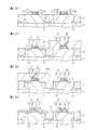
次に、第1の実施例のトランジスタの製造方法について説明する。図1(A)〜図1(K)は、第1の実施例のトランジスタ製造方法を説明するための概略断面図である。 Next, a method for manufacturing the transistor of the first embodiment will be described. FIG. 1A to FIG. 1K are schematic cross-sectional views for explaining the transistor manufacturing method of the first embodiment.
図1(A)に示すように、例えばn型シリコン基板1に、例えばSTIにより素子分離領域2を形成し、相互に隣接する2つの活性領域にそれぞれp型ウェル3及びn型ウェル23を形成する。ここでp型ウェル3は、例えば、Bを加速エネルギ150keV、ドーズ量1×10¹⁵atoms/cm2で注入して形成でき、n型ウェル23は、例えば、Pを加速エネルギ300keV、ドーズ量1×1013atoms/cm2で注入して形成できる。
As shown in FIG. 1A, for example, an
活性領域表面を熱酸化し、p型ウェル3及びn型ウェル23表面にゲート絶縁膜となる酸化シリコン膜を形成する。さらに酸化シリコン膜上に例えばCVDでポリシリコン膜を形成し、ポリシリコン膜を、写真食刻法を用いたエッチングでパターンニングする。ゲート電極がポリシリコンやアモルファスシリコンの場合には、例えばHBrを用いたガスプラズマによるRIEが適しており、酸化シリコン膜でエッチングを止める。露出した酸化シリコン膜は、必要に応じて等方性エッチングする。
The surface of the active region is thermally oxidized to form a silicon oxide film serving as a gate insulating film on the surfaces of the p-
なお、ここで、ゲート絶縁膜は、酸化シリコン膜の他に、例えば、酸化シリコン膜に窒素を導入した酸窒化シリコン膜でもよく、また例えば、酸化シリコン膜や酸窒化シリコン膜上に、HfやLa等を含む高誘電体膜を積層した構造としてもよい。また、ゲート電極は、ポリシリコンの他に、例えばアモルファスシリコンや、シリサイド、メタルゲートとしてもよい。 Here, the gate insulating film may be, for example, a silicon oxynitride film in which nitrogen is introduced into the silicon oxide film, in addition to the silicon oxide film. A high dielectric film containing La or the like may be stacked. In addition to polysilicon, the gate electrode may be amorphous silicon, silicide, or metal gate, for example.
このようにして、p型ウェル3及びn型ウェル23上にそれぞれ、ゲート絶縁膜4にゲート電極5が積層されたゲート6、及び、ゲート絶縁膜24にゲート電極25が積層されたゲート26が形成される。
In this manner, the
次に、図1(B)に示すように、ゲート6及び26を覆って全面に、HfO2を原子層堆積(ALD)で厚さ2nm形成して、バリア絶縁膜7を形成する。ALDは、例えば、基板温度を300℃とし、HfCl4とH2Oを交互に供給することにより行われる。なお、有機金属化学気相堆積(MOCVD)でHfO2膜を形成することもできる。
Next, as shown in FIG. 1B, HfO 2 is formed to a thickness of 2 nm by atomic layer deposition (ALD) over the entire surface covering the
次に、図1(C)に示すように、バリア絶縁膜7の上に、酸化シリコンからなるスペーサ絶縁膜8を、例えば、SiH4とO2を材料とし温度を425℃としたCVDで、厚さ7nm形成する。
Next, as shown in FIG. 1C, a
次に、図1(D)に示すように、CとFとを含むフロロカーボン系のガスプラズマを用いたRIEで、スペーサ絶縁膜8を異方性エッチングして、ゲート6の側壁上及びゲート26の側壁上の部分のみ残すことにより、ゲート6の側壁上にスペーサ9を、ゲート26の側壁上にスペーサ29を形成する。このRIEは、充分高い選択比を持って、バリア絶縁膜7の表面で停止させることができる。RIEに用いるガスとして、例えば、CHF3にArを加えたものや、CF4を用いることができる。
Next, as shown in FIG. 1D, the
例えばCF4によるエッチング速度は、SiO2では90nm/minであるのに対し、HfO2では2nm/minであることが知られている(Maeda et al. SSDM 2003)。 For example, it is known that the etching rate by CF 4 is 90 nm / min for SiO 2 and 2 nm / min for HfO 2 (Maeda et al. SSDM 2003).
HfO2は、イオン阻止能力が高い。SRIM(IBMがフリーウェアとして公開しており、イオンの固体中での飛程をモンテカルロ法で計算するシミュレーションソフト)による計算の結果、例えばBを10keVで打ち込んだ場合、SiO2中、HfO2中への侵入深さは、それぞれ、40nm、17.9nmである。また例えばAsを10keVで打ち込んだ場合、SiO2中、HfO2中への侵入深さは、それぞれ、11.7nm、5.4nmである。このように、HfO2に注入されたイオンは、SiO2の約半分の深さまでしか侵入できない傾向がある。 HfO 2 has a high ion blocking ability. As a result of calculation by SRIM (simulation software released by IBM as freeware and calculating the range of ions in a solid by the Monte Carlo method), for example, when B is implanted at 10 keV, in SiO 2 and in HfO 2 The penetration depths are 40 nm and 17.9 nm, respectively. For example, when As is implanted at 10 keV, the penetration depths into SiO 2 and HfO 2 are 11.7 nm and 5.4 nm, respectively. Thus, ions implanted into HfO 2 tend to penetrate only about half the depth of SiO 2 .
HfO2からなるバリア絶縁膜7により、フロロカーボン系のガスプラズマを用いたRIEによるスペーサ絶縁膜8のエッチング時に、炭素がシリコン基板表面に達することが妨げられ、変質ダメージ層の形成が抑制される。
The
次に、図1(E)に示すように、例えば130℃の熱濃硫酸と過酸化水素水の混合溶液に20分間浸漬するウエットエッチングにより、p型ウェル3、n型ウェル23、ゲート電極5、25、及び、素子分離領域2上の、露出したバリア絶縁膜7を除去する。スペーサ9、29とゲート6、26側壁との間、スペーサ9、29とp型ウェル3、n型ウェル23との間に挟まれた部分のバリア絶縁膜10、30は残る。
Next, as shown in FIG. 1E, for example, p-
なお、このウエットエッチングの温度は130℃に限らない。望ましい温度条件として110℃以上150℃以下の熱濃硫酸と過酸化水素水の混合溶液で、HfO2が除去される。ウエットエッチングであるため、基板やゲート電極、素子分離領域へのダメージを抑えて、HfO2を除去できる。 The wet etching temperature is not limited to 130 ° C. As a desirable temperature condition, HfO 2 is removed with a mixed solution of hot concentrated sulfuric acid and hydrogen peroxide water at 110 ° C. or higher and 150 ° C. or lower. Because of wet etching, HfO 2 can be removed while suppressing damage to the substrate, the gate electrode, and the element isolation region.
このようにして、ゲート6の側壁上に、側壁側からバリア絶縁膜10、スペーサ9が積層されたスペーサ構造11が形成され、ゲート26の側壁上に、側壁側からバリア絶縁膜30、スペーサ29が積層されたスペーサ構造31が形成される。スペーサ9、29とp型ウェル3、n型ウェル23との間に、それぞれ、バリア絶縁膜10、30が介在する。
In this way, the
次に、図1(F)に示すように、n型ウェル23側の活性領域をホトレジストPR1で覆い、ゲート6及びスペーサ構造11をマスクとして、p型ウェル3に、n型不純物として例えばAsを、加速エネルギ3keV、ドーズ量1×10¹⁵atoms/cm2で注入して、n型エクステンション12を形成する。
Next, as shown in FIG. 1F, the active region on the n-type well 23 side is covered with a photoresist PR1, and the
次に、図1(G)に示すように、p型ウェル3側の活性領域をホトレジストPR2で覆い、ゲート26及びスペーサ構造31をマスクとして、n型ウェル23に、p型不純物として例えばBを、加速エネルギ0.5keV、ドーズ量1×10¹⁵atoms/cm2で注入して、p型エクステンション32を形成する。
Next, as shown in FIG. 1G, the active region on the p-type well 3 side is covered with a photoresist PR2, and the
次に、図1(H)に示すように、ゲート6とスペーサ構造11、及び、ゲート26とスペーサ構造31を覆って全面に、酸化シリコンからなるサイドウォール絶縁膜13を、例えばCVDで厚さ50nm形成する。
Next, as shown in FIG. 1H, a
次に、図1(I)に示すように、フロロカーボン系のガスプラズマを用いたRIEで、サイドウォール絶縁膜13を異方性エッチングして、スペーサ構造11及び31の側壁上の部分のみを残すことにより、サイドウォール14、34を形成する。なお、サイドウォールを形成する膜は酸化シリコン膜に限らず、必要に応じて、酸窒化シリコン膜や窒化シリコン膜としてもよい。
Next, as shown in FIG. 1I, the
次に、図1(J)に示すように、n型ウェル23側の活性領域をホトレジストPR3で覆い、ゲート6、スペーサ構造11、及びサイドウォール14をマスクとし、n型不純物として例えばPを加速エネルギ6keV(またはAsを加速エネルギ20keV)、ドーズ量1×10¹⁶atoms/cm2で注入して、エクステンション12よりも高濃度で、深い領域に、n型ソース/ドレイン領域15を形成する。なお、ゲート電極5上面にもn型不純物がドープされる。
Next, as shown in FIG. 1J, the active region on the n-type well 23 side is covered with a photoresist PR3, and the
次に、図1(K)に示すように、p型ウェル3側の活性領域をホトレジストPR4で覆い、ゲート26、スペーサ構造31、及びサイドウォール34をマスクとし、p型不純物として例えばBを、加速エネルギ3keV、ドーズ量4×10¹⁵atoms/cm2で注入して、エクステンション32よりも高濃度で、深い領域に、p型ソース/ドレイン領域35を形成する。なお、ゲート電極25上面にもp型不純物がドープされる。
Next, as shown in FIG. 1K, the active region on the p-type well 3 side is covered with a photoresist PR4, the
このようにして、p型ウェル3側にnMOSトランジスタが形成され、n型ウェル23側にpMOSトランジスタが形成される。この後、ソース/ドレイン領域15、35、及び、ゲート電極5、25の表面をシリサイド化し、その上に層間絶縁膜を形成する。層間絶縁膜にコンタクト孔をエッチングし、導電性プラグを埋め込む。さらに、上方に配線層が形成される。シリサイド化、層間絶縁膜、配線層の形成等には、公知の方法を用いることができる。
In this way, an nMOS transistor is formed on the p-type well 3 side, and a pMOS transistor is formed on the n-type well 23 side. Thereafter, the surfaces of the source /
以上説明したように、スペーサ絶縁膜の下にバリア絶縁膜が配置された状態で、スペーサを形成する異方性エッチングを行うことにより、基板表面の変質ダメージ層の形成が抑制され、エクステンションを良好に形成できる。 As described above, by performing anisotropic etching to form a spacer in a state where a barrier insulating film is disposed under the spacer insulating film, formation of a damaged layer on the substrate surface is suppressed, and the extension is improved. Can be formed.
なお、実施例のスペーサ構造では、スペーサと、基板表面及びゲート側壁との間に、バリア絶縁膜が介在する。このため、斜め注入でエクステンションを形成する場合において、スペーサを透過したイオンがゲート直下のゲート絶縁膜にダメージを与えることを抑制可能である。 In the spacer structure of the embodiment, a barrier insulating film is interposed between the spacer and the substrate surface and the gate side wall. For this reason, in the case where the extension is formed by oblique implantation, it is possible to prevent the ions that have passed through the spacer from damaging the gate insulating film immediately below the gate.
なお、上記実施例では、バリア絶縁膜の厚さを例えば2nmとした。図4(B)を参照して説明したように、変質ダメージ層の深さはシリコン基板表面から2nm程度であるので、シリコンよりも物質透過防止能力が高いバリア絶縁膜の厚さは、例えば変質ダメージ層の深さと同程度である2nmにすればよいであろう。 In the above embodiment, the thickness of the barrier insulating film is set to 2 nm, for example. As described with reference to FIG. 4B, since the depth of the altered damage layer is about 2 nm from the surface of the silicon substrate, the thickness of the barrier insulating film having a material permeation preventing ability higher than that of silicon is, for example, altered. It should be 2 nm, which is about the same as the depth of the damaged layer.
上述のイオン阻止能力を目安として、バリア絶縁膜の厚さは、変質ダメージ層の深さの半分程度の1nm程度まで薄くしてもよいであろう。なお、バリア絶縁膜を不必要に厚くする必要もないので、バリア絶縁膜の厚さの上限は、例えば変質ダメージ層の深さの1.5倍程度の3nm程度とすればよいであろう。つまり、バリア絶縁膜の厚さは、1nm以上3nm以下の範囲とすればよいであろう。 Using the above-described ion blocking ability as a guide, the thickness of the barrier insulating film may be reduced to about 1 nm, which is about half the depth of the damaged layer. Since the barrier insulating film does not need to be unnecessarily thick, the upper limit of the thickness of the barrier insulating film may be, for example, about 3 nm, which is about 1.5 times the depth of the damaged layer. That is, the thickness of the barrier insulating film may be in the range of 1 nm to 3 nm.
なお、バリア絶縁膜を堆積する前に、厚さ1nm以下の酸化シリコン膜、酸窒化シリコン膜、または窒化シリコン膜を堆積し、その上に厚さ1nm以上2nm以下のバリア絶縁膜を積層するようにしてもよい。 Note that before the barrier insulating film is deposited, a silicon oxide film, a silicon oxynitride film, or a silicon nitride film having a thickness of 1 nm or less is deposited, and a barrier insulating film having a thickness of 1 nm to 2 nm is stacked thereon. It may be.
バリア絶縁膜とスペーサとの積層の厚さは、上述の実施例では9nm(バリア絶縁膜2nm+スペーサ絶縁膜7nm)としたが、厚さはこれに限らず、8nm以上12nm以下の範囲であれば好適であろう。
The thickness of the stack of the barrier insulating film and the spacer is 9 nm in the above-described embodiment (
上述の実施例では、HfO2からなるバリア絶縁膜を、熱濃硫酸と過酸化水素水との混合液によりエッチングしたが、他の薬液でエッチングしてもよい。例えば、110℃以上180℃以下の熱濃硫酸や、130℃以上180℃以下の熱濃燐酸、あるいはフッ化水素水を用いても、HfO2が除去される。ただし、フッ化水素水を用いる場合は、スペーサやSTIの後退が生じるので注意が必要である。 In the above-described embodiment, the barrier insulating film made of HfO 2 is etched with a mixed solution of hot concentrated sulfuric acid and hydrogen peroxide solution, but may be etched with another chemical solution. For example, HfO 2 can also be removed by using hot concentrated sulfuric acid of 110 ° C. or higher and 180 ° C. or lower, hot concentrated phosphoric acid of 130 ° C. or higher and 180 ° C. or lower, or hydrogen fluoride water. However, when hydrogen fluoride water is used, care must be taken because the spacers and STI retract.
HfO2を、濃硫酸を主成分として含む薬液(濃硫酸や、濃硫酸と過酸化水素水の混合溶液など)でエッチングできる温度条件は、80℃以上200℃以下の範囲となろう。実験事実として、80℃より低温ではエッチング速度が遅くなりすぎる。また温度上限は不必要に高くしなくてよく、例えば200℃程度までなら通常の薬液処理槽での処理が容易である。 The temperature condition under which HfO 2 can be etched with a chemical solution containing concentrated sulfuric acid as a main component (such as concentrated sulfuric acid or a mixed solution of concentrated sulfuric acid and hydrogen peroxide) will be in the range of 80 ° C. to 200 ° C. As an experimental fact, the etching rate becomes too slow at a temperature lower than 80 ° C. The upper limit of the temperature does not need to be unnecessarily high. For example, when the temperature is up to about 200 ° C., the treatment in a normal chemical solution treatment tank is easy.
上述の実施例では、バリア絶縁膜形成工程や、スペーサ絶縁膜形成工程を、HfO2が結晶化しない、800℃より低い温度(より好ましくは500℃以下)で行っており、HfO2は非晶質状態を保つ。非晶質状態のHfO2は、薬液で容易に溶解除去できる。 In the above embodiment, and the barrier insulating film forming step, the spacer insulating film formation step, HfO 2 is not crystallized, and performed at lower than 800 ° C. temperature (more preferably 500 ° C. or less), HfO 2 is amorphous Maintain quality. The amorphous HfO 2 can be easily dissolved and removed with a chemical solution.
なお、例えば、スペーサとなる酸化シリコン膜をCVDで形成するときの温度が充分に下げられず、HfO2が仮に結晶化したとしても、スペーサを残すRIE時のプラズマ曝露で、HfO2を非晶質にすることができる。非晶質となったHfO2を、容易に溶解除去することができる。 Incidentally, for example, the temperature can not be sufficiently lowered at the time of forming a silicon oxide film serving as a spacer in CVD, even HfO 2 was tentatively crystallized during RIE to leave spacers in plasma exposure, the HfO 2 amorphous Can be quality. The amorphous HfO 2 can be easily dissolved and removed.
なお、HfO2をウエットエッチングで除去する以外の方法でも、基板やゲート電極、素子分離領域へのダメージを抑えて、HfO2を除去できる。例えば、CCl4中で500℃に加熱し、HfO2をHfCl4に変化させ、昇華させて除去することができる。HfCl4は320℃の加熱によって昇華することが知られている。このように、塩素を含むガスとの熱反応でいったん塩化物とし、この塩化物を昇華させることにより、HfO2を除去することもできる。 It should be noted that HfO 2 can be removed while suppressing damage to the substrate, the gate electrode, and the element isolation region by a method other than removing HfO 2 by wet etching. For example, it can be removed by heating to 500 ° C. in CCl 4 to change HfO 2 to HfCl 4 and sublimate. It is known that HfCl 4 sublimes by heating at 320 ° C. Thus, HfO 2 can be removed by once converting into chloride by a thermal reaction with a gas containing chlorine and sublimating the chloride.
なお、上述の実施例では、バリア絶縁膜の材料としてHfO2を用いたが、他の材料を用いることもできるであろう。基本的に、HfO2のように、原子番号の大きな重い原子の酸化物を用いると、物質透過防止能力の高いバリア絶縁膜ができるであろう。なお、酸化物に限らず、窒化物や酸窒化物であってもよいであろう。 In the above embodiment, HfO 2 is used as the material for the barrier insulating film, but other materials may be used. Basically, if an oxide of a heavy atom having a large atomic number such as HfO 2 is used, a barrier insulating film having a high material permeation preventing capability will be formed. Note that not only oxides but also nitrides and oxynitrides may be used.
このような材料のうち、特に、高誘電体材料が、実際の素子作製に好適であろう。例えば、Sc、Ti、Sr、Y、Zr、Hf、Ta、Laのいずれかまたはこれらの合金の、酸化物、窒化物、または酸窒化物が好適であろう。HfO2の他には、例えば、Sc2O3、TiO2、SrO、Y2O5、ZrO2、Ta2O5、La2O5が挙げられる。なお、Ti、Zrは、Hfと同族である。 Among these materials, a high dielectric material will be particularly suitable for actual device fabrication. For example, an oxide, nitride, or oxynitride of any of Sc, Ti, Sr, Y, Zr, Hf, Ta, La or alloys thereof may be suitable. In addition to HfO 2 , for example, Sc 2 O 3 , TiO 2 , SrO, Y 2 O 5 , ZrO 2 , Ta 2 O 5 , La 2 O 5 may be mentioned. Ti and Zr are in the same family as Hf.
これらの材料をバリア絶縁膜に用いた場合の除去方法について説明する。Ta2O5、SrOはアルカリに溶解し、Y2O5、La2O5は酸に溶解し、Sc2O3は熱酸に溶解し、TiO2、ZrO2は硫酸に溶解するため、酸またはアルカリ薬液によるウエットエッチングでの除去が可能である。 A removal method when these materials are used for the barrier insulating film will be described. Ta 2 O 5 and SrO are dissolved in alkali, Y 2 O 5 and La 2 O 5 are dissolved in acid, Sc 2 O 3 is dissolved in hot acid, and TiO 2 and ZrO 2 are dissolved in sulfuric acid. Removal by wet etching with an acid or alkali chemical solution is possible.
なお、ウエットエッチングで除去できないバリア絶縁膜に対しては、以下のような除去方法も用いられよう。TiO2、ZrO2、Ta2O5を用いた場合、塩化物や臭化物は400℃以下で気化する。このため、例えば、塩素を含むガスや臭素を含むガスのプラズマによるRIEで、ハロゲン化物にして除去することができよう。このように、(炭素を含まない)ハロゲン化合物またはハロゲンガスのプラズマまたはラジカルによるバリア絶縁膜の除去方法も有効であろう。また、基板を加熱することが効果的であろう。なお、このような方法はHfO2にも適用可能である。 For the barrier insulating film that cannot be removed by wet etching, the following removal method may be used. When TiO 2 , ZrO 2 , or Ta 2 O 5 is used, chlorides and bromides are vaporized at 400 ° C. or lower. For this reason, for example, it can be removed as a halide by RIE using plasma of a gas containing chlorine or a gas containing bromine. Thus, a method of removing the barrier insulating film by plasma or radical of halogen compound (containing no carbon) or halogen gas will be effective. It may also be effective to heat the substrate. Such a method is also applicable to HfO 2 .
蒸気圧が低くてガス化が困難な場合は、不活性ガス(Ar、Xeなど)のイオン照射(ミリング)によって除去することもできよう。 If gasification is difficult due to low vapor pressure, it can be removed by ion irradiation (milling) of an inert gas (Ar, Xe, etc.).
次に、第2実施例のトランジスタの製造方法について説明する。図2(A)〜図2(E)は、第2の実施例のトランジスタ製造方法を説明するための概略断面図である。第1の実施例との違いは、ゲート絶縁膜として高誘電体材料を含む膜を用い、ゲート絶縁膜とバリア絶縁膜とを共通とすることである。 Next, a method for manufacturing the transistor of the second embodiment will be described. 2A to 2E are schematic cross-sectional views for explaining the transistor manufacturing method of the second embodiment. The difference from the first embodiment is that a film containing a high dielectric material is used as the gate insulating film, and the gate insulating film and the barrier insulating film are shared.
図2(A)に示すように、第1の実施例と同様にして、p型ウェル3及びn型ウェル23を形成する。p型ウェル3及びn型ウェル23を覆って全面に、例えばHfO2膜からなるバリア絶縁膜(ゲート絶縁膜)7aを形成し、さらにバリア絶縁膜7a上に例えばポリシリコン膜を形成し、ポリシリコン膜をパターンニングして、p型ウェル3側にゲート電極5a、n型ウェル23側にゲート電極25aを形成する。
As shown in FIG. 2A, the p-
次に、図2(B)に示すように、ゲート電極5a及び25aを覆って、バリア絶縁膜7a上全面に、スペーサ絶縁膜8aを形成する。 Next, as shown in FIG. 2B, a spacer insulating film 8a is formed on the entire surface of the barrier insulating film 7a so as to cover the gate electrodes 5a and 25a.
次に、図2(C)に示すように、フロロカーボン系のガスプラズマを用いたRIEで、スペーサ絶縁膜8aをエッチングして、ゲート電極5aの側壁上にスペーサ9aを、ゲート電極25aの側壁上にスペーサ29aを形成する。 Next, as shown in FIG. 2C, the spacer insulating film 8a is etched by RIE using a fluorocarbon-based gas plasma so that the spacer 9a is formed on the side wall of the gate electrode 5a and the side wall of the gate electrode 25a. A spacer 29a is formed on the substrate.
スペーサ絶縁膜8aの形成方法、及び、スペーサ9a、29aを残すエッチング方法は、第1の実施例と同様である。バリア絶縁膜7aにより、第1の実施例と同様に、炭素がシリコン基板表面に達することが妨げられ、変質ダメージ層の形成が抑制される。 The method for forming the spacer insulating film 8a and the etching method for leaving the spacers 9a and 29a are the same as in the first embodiment. As in the first embodiment, the barrier insulating film 7a prevents carbon from reaching the surface of the silicon substrate and suppresses the formation of a damaged layer.
次に、図2(D)に示すように、p型ウェル3、n型ウェル23、及び、素子分離領域2上の、露出したバリア絶縁膜(ゲート絶縁膜)7aを、第1の実施例と同様にして除去する。スペーサ9a及びゲート電極5aとp型ウェル3との間にゲート絶縁膜4aが残り、スペーサ29a及びゲート電極25aとn型ウェル23との間にゲート絶縁膜24aが残る。
Next, as shown in FIG. 2D, the exposed barrier insulating film (gate insulating film) 7a on the p-
ゲート電極5a側壁上に形成されたスペーサ9aの下に、バリア絶縁膜としてゲート絶縁膜4aの端部が配置されたスペーサ構造11aと、ゲート電極25a側壁上に形成されたスペーサ29aの下に、バリア絶縁膜としてゲート絶縁膜24aの端部が配置されたスペーサ構造31aとが形成される。ゲート電極5aとゲート絶縁膜4aがゲート6aを構成し、ゲート電極25aとゲート絶縁膜24aがゲート26aを構成する。
Below the spacer 9a formed on the side wall of the gate electrode 5a, a
以後、図2(E)に示すように、ゲート6a、スペーサ構造11aをマスクとするイオン注入でp型ウェル3側のn型エクステンション12aが形成され、ゲート26a、スペーサ構造31aをマスクとするイオン注入でn型ウェル23側のp型エクステンション32aが形成され、スペーサ構造11a、31aの側壁上にサイドウォール14a、34aがそれぞれ形成され、ゲート電極5a、スペーサ構造11a、サイドウォール14aをマスクとするイオン注入でp型ウェル3側のn型ソース/ドレイン領域15aが形成され、ゲート電極25a、スペーサ構造31a、サイドウォール34aをマスクとするイオン注入でn型ウェル23側のp型ソース/ドレイン領域35aが形成されて、nMOSトランジスタ及びpMOSトランジスタが形成される。
Thereafter, as shown in FIG. 2E, the n-
なお、第2の実施例のスペーサ構造でも、第1の実施例と同様に、スペーサと、基板表面との間に、バリア絶縁膜が介在する。このため、斜め注入でエクステンションを形成する場合において、スペーサを透過したイオンがゲート直下のゲート絶縁膜にダメージを与えることを抑制可能である。 In the spacer structure of the second embodiment, as in the first embodiment, a barrier insulating film is interposed between the spacer and the substrate surface. For this reason, in the case where the extension is formed by oblique implantation, it is possible to prevent the ions that have passed through the spacer from damaging the gate insulating film immediately below the gate.
なお、第2の実施例で、バリア絶縁膜(ゲート絶縁膜)は、基板表面の熱酸化シリコン膜の上に、Hf等を含む高誘電体膜を積層した構造としてもよい。例えば、高誘電体膜を除去した下に、熱酸化シリコン膜が残る。 In the second embodiment, the barrier insulating film (gate insulating film) may have a structure in which a high dielectric film containing Hf or the like is laminated on a thermally oxidized silicon film on the substrate surface. For example, a thermally oxidized silicon film remains after the high dielectric film is removed.
なお、以上の実施例で、プレーナ型のトランジスタについて説明したが、実施例のスペーサ構造は、それに限らず、シリコンオンインシュレーター(SOI)やシリコンゲルマニウム上の歪シリコン、エレベーティッドSiGeなどのデバイスに利用することもできよう。 In the above embodiment, the planar type transistor has been described. However, the spacer structure of the embodiment is not limited to this, and is used for devices such as silicon-on-insulator (SOI), strained silicon on silicon germanium, and elevated SiGe. You can also do it.
以上実施例に沿って本発明を説明したが、本発明はこれらに制限されるものではない。例えば、種々の変更、改良、組み合わせ等が可能なことは当業者に自明であろう。 Although the present invention has been described with reference to the embodiments, the present invention is not limited thereto. It will be apparent to those skilled in the art that various modifications, improvements, combinations, and the like can be made.
以下、本発明の特徴を付記する。
(付記1)
半導体基板上にゲート絶縁膜を形成する工程と、
前記ゲート絶縁膜上にゲート電極を形成する工程と、
前記ゲート絶縁膜に前記ゲート電極が積層されたゲートを覆って、前記半導体基板上に、高誘電体材料を含むバリア絶縁膜を形成する工程と、
前記バリア絶縁膜上に、スペーサ絶縁膜を形成する工程と、
前記スペーサ絶縁膜を、異方性エッチングして、前記ゲートの側壁上にスペーサを残して除去する工程と、
露出した前記バリア絶縁膜を除去する工程と、
前記ゲート及びスペーサをマスクとして、前記半導体基板に不純物を注入し、エクステンションを形成する工程と、
前記ゲート及びスペーサを覆って、前記半導体基板上に、サイドウォール絶縁膜を形成する工程と、
前記サイドウォール絶縁膜を、異方性エッチングして、前記スペーサの側壁上にサイドウォールを残して除去する工程と、
前記ゲート、スペーサ、及びサイドウォールをマスクとして、前記半導体基板に、前記エクステンションの形成時よりも高い濃度の不純物を注入し、ソース/ドレイン領域を形成する工程と
を有する半導体装置の製造方法。
(付記2)
前記半導体基板はシリコン基板であり、前記スペーサ絶縁膜を除去する工程において、前記異方性エッチングは、フロロカーボン系のガスプラズマを用いた反応性イオンエッチングである付記1に記載の半導体装置の製造方法。
(付記3)
前記バリア絶縁膜を除去する工程は、ウエットエッチングで前記バリア絶縁膜を除去する付記1または2に記載の半導体装置の製造方法。
(付記4)
前記バリア絶縁膜を形成する工程で、前記高誘電体材料は、Sc、Ti、Sr、Y、Zr、Hf、Ta、Laのいずれかまたはこれらの合金の、酸化物、窒化物、または酸窒化物である付記1または2に記載の半導体装置の製造方法。
(付記5)
前記バリア絶縁膜を除去する工程は、酸またはアルカリ薬液によるウエットエッチングで前記バリア絶縁膜を除去する付記4に記載の半導体装置の製造方法。
(付記6)
前記バリア絶縁膜を除去する工程は、炭素を含まないハロゲン化合物またはハロゲンガスのプラズマまたはラジカルにより前記バリア絶縁膜を除去する付記4に記載の半導体装置の製造方法。
(付記7)
前記バリア絶縁膜を除去する工程は、不活性ガスのイオン照射で前記バリア絶縁膜を除去する付記4に記載の半導体装置の製造方法。
(付記8)
前記バリア絶縁膜を形成する工程で、前記高誘電体材料はHfO2である付記4に記載の半導体装置の製造方法。
(付記9)
前記バリア絶縁膜を除去する工程は、80℃以上200℃以下の濃硫酸を含む薬液によるウエットエッチングで前記バリア絶縁膜を除去する付記8に記載の半導体装置の製造方法。
(付記10)
前記バリア絶縁膜を除去する工程は、110℃以上150℃以下の熱濃硫酸と過酸化水素水との混合液、110℃以上180℃以下の熱濃硫酸、130℃以上180℃以下の熱濃燐酸、またはフッ化水素水によるウエットエッチングで、前記バリア絶縁膜を除去する付記8に記載の半導体装置の製造方法。
(付記11)
前記バリア絶縁膜を除去する工程は、前記バリア絶縁膜を、塩素を含むガスと反応させて塩化物とし、該塩化物を昇華させることにより除去する付記8に記載の半導体装置の製造方法。
(付記12)
前記バリア絶縁膜を形成する工程で、前記高誘電体材料は、HfO2、TiO2、ZrO2、またはTa2O5であり、前記バリア絶縁膜を除去する工程は、該バリア絶縁膜を、炭素を含まず塩素または臭素を含むガスのプラズマによる反応性イオンエッチングで除去する付記4に記載の半導体装置の製造方法。
(付記13)
前記バリア絶縁膜の厚さは、1nm以上3nm以下である付記1〜12のいずれか1つに記載の半導体装置の製造方法。
(付記14)
さらに、前記バリア絶縁膜を形成する工程の前に、前記ゲート電極が積層されたゲートを覆って、厚さ1nm以下の酸化シリコン膜、酸窒化シリコン膜、または窒化シリコン膜を形成する工程を有し、この膜の上に、厚さ1nm以上2nm以下の該バリア絶縁膜を形成する付記1〜12のいずれか1つに記載の半導体装置の製造方法。
(付記15)
前記バリア絶縁膜と前記スペーサ絶縁膜との積層の厚さは、8nm以上12nm以下である付記1〜14のいずれか1つに記載の半導体装置の製造方法。
(付記16)
半導体基板上に、高誘電体材料を含むゲート絶縁膜を形成する工程と、
前記ゲート絶縁膜上にゲート電極を形成する工程と、
前記ゲート電極を覆って、前記ゲート絶縁膜上に、スペーサ絶縁膜を形成する工程と、
前記スペーサ絶縁膜を、異方性エッチングして、前記ゲート電極の側壁上にスペーサを残して除去する工程と、
露出した前記ゲート絶縁膜を、前記スペーサ及び前記ゲート電極の下に配置された部分を残して除去する工程と、
前記ゲート絶縁膜に前記ゲート電極が積層されたゲート、及び前記スペーサをマスクとして、前記半導体基板に不純物を注入し、エクステンションを形成する工程と、
前記ゲート及びスペーサを覆って、前記半導体基板上に、サイドウォール絶縁膜を形成する工程と、
前記サイドウォール絶縁膜を、異方性エッチングして、前記スペーサの側壁上にサイドウォールを残して除去する工程と、
前記ゲート、スペーサ、及びサイドウォールをマスクとして、前記半導体基板に、前記エクステンションの形成時よりも高い濃度の不純物を注入し、ソース/ドレイン領域を形成する工程と
を有する半導体装置の製造方法。
The features of the present invention will be described below.
(Appendix 1)
Forming a gate insulating film on the semiconductor substrate;
Forming a gate electrode on the gate insulating film;
Covering the gate in which the gate electrode is stacked on the gate insulating film, and forming a barrier insulating film containing a high dielectric material on the semiconductor substrate;
Forming a spacer insulating film on the barrier insulating film;
Removing the spacer insulating film by anisotropic etching, leaving a spacer on the side wall of the gate; and
Removing the exposed barrier insulating film;
Using the gate and spacer as a mask, implanting impurities into the semiconductor substrate, and forming an extension;
Forming a sidewall insulating film on the semiconductor substrate so as to cover the gate and the spacer;
Removing the sidewall insulating film by anisotropic etching to leave a sidewall on the sidewall of the spacer; and
A method of manufacturing a semiconductor device, comprising: implanting impurities having a higher concentration than the formation of the extension into the semiconductor substrate using the gate, the spacer, and the sidewall as a mask to form source / drain regions.
(Appendix 2)
The method for manufacturing a semiconductor device according to
(Appendix 3)
The method for manufacturing a semiconductor device according to
(Appendix 4)
In the step of forming the barrier insulating film, the high dielectric material is made of any of Sc, Ti, Sr, Y, Zr, Hf, Ta, La, or an alloy thereof, oxide, nitride, or oxynitride The method for manufacturing a semiconductor device according to
(Appendix 5)
The method of manufacturing a semiconductor device according to
(Appendix 6)
5. The method of manufacturing a semiconductor device according to
(Appendix 7)
The method for manufacturing a semiconductor device according to
(Appendix 8)
The method for manufacturing a semiconductor device according to
(Appendix 9)
9. The method of manufacturing a semiconductor device according to
(Appendix 10)
The step of removing the barrier insulating film includes a mixed solution of hot concentrated sulfuric acid of 110 ° C. to 150 ° C. and hydrogen peroxide, hot concentrated sulfuric acid of 110 ° C. to 180 ° C., and hot concentrated of 130 ° C. to 180 °
(Appendix 11)
The method of manufacturing a semiconductor device according to
(Appendix 12)
In the step of forming the barrier insulating film, the high dielectric material is HfO 2 , TiO 2 , ZrO 2 , or Ta 2 O 5 , and the step of removing the barrier insulating film includes the step of forming the barrier insulating film, The method for manufacturing a semiconductor device according to
(Appendix 13)
13. The method of manufacturing a semiconductor device according to any one of
(Appendix 14)
Furthermore, before the step of forming the barrier insulating film, there is a step of forming a silicon oxide film, a silicon oxynitride film, or a silicon nitride film having a thickness of 1 nm or less so as to cover the gate on which the gate electrode is stacked. The method for manufacturing a semiconductor device according to any one of
(Appendix 15)
The method for manufacturing a semiconductor device according to any one of
(Appendix 16)
Forming a gate insulating film containing a high dielectric material on a semiconductor substrate;
Forming a gate electrode on the gate insulating film;
Covering the gate electrode and forming a spacer insulating film on the gate insulating film;
Removing the spacer insulating film by anisotropic etching, leaving a spacer on the side wall of the gate electrode; and
Removing the exposed gate insulating film, leaving a portion disposed under the spacer and the gate electrode;
Injecting impurities into the semiconductor substrate using the gate in which the gate electrode is stacked on the gate insulating film and the spacer as a mask, and forming an extension;
Forming a sidewall insulating film on the semiconductor substrate so as to cover the gate and the spacer;
Removing the sidewall insulating film by anisotropic etching to leave a sidewall on the sidewall of the spacer; and
A method of manufacturing a semiconductor device, comprising: implanting impurities having a higher concentration than the formation of the extension into the semiconductor substrate using the gate, the spacer, and the sidewall as a mask to form source / drain regions.
1 シリコン基板
2 素子分離領域
3 p型ウェル
23 n型ウェル
4、24 ゲート絶縁膜
5、25 ゲート電極
6、26 ゲート
7 バリア絶縁膜
8 酸化シリコン膜(スペーサ絶縁膜)
9、29 スペーサ
10、30 バリア絶縁膜
11、31 スペーサ構造
12、32 エクステンション
13 酸化シリコン膜(サイドウォール絶縁膜)
14、34 サイドウォール
15、35 ソース/ドレイン領域
DESCRIPTION OF
9, 29
14, 34
Claims (6)
前記ゲート絶縁膜上にゲート電極を形成する工程と、
前記ゲート絶縁膜に前記ゲート電極が積層されたゲートを覆って、前記半導体基板上に、高誘電体材料を含むバリア絶縁膜を形成する工程と、
前記バリア絶縁膜上に、スペーサ絶縁膜を形成する工程と、
前記スペーサ絶縁膜を、異方性エッチングして、前記ゲートの側壁上にスペーサを残して除去する工程と、
露出した前記バリア絶縁膜を除去する工程と、
前記ゲート及びスペーサをマスクとして、前記半導体基板に不純物を注入し、エクステンションを形成する工程と、
前記ゲート及びスペーサを覆って、前記半導体基板上に、サイドウォール絶縁膜を形成する工程と、
前記サイドウォール絶縁膜を、異方性エッチングして、前記スペーサの側壁上にサイドウォールを残して除去する工程と、
前記ゲート、スペーサ、及びサイドウォールをマスクとして、前記半導体基板に、前記エクステンションの形成時よりも高い濃度の不純物を注入し、ソース/ドレイン領域を形成する工程と
を有する半導体装置の製造方法。 Forming a gate insulating film on the semiconductor substrate;
Forming a gate electrode on the gate insulating film;
Covering the gate in which the gate electrode is stacked on the gate insulating film, and forming a barrier insulating film containing a high dielectric material on the semiconductor substrate;
Forming a spacer insulating film on the barrier insulating film;
Removing the spacer insulating film by anisotropic etching, leaving a spacer on the side wall of the gate; and
Removing the exposed barrier insulating film;
Using the gate and spacer as a mask, implanting impurities into the semiconductor substrate, and forming an extension;
Forming a sidewall insulating film on the semiconductor substrate so as to cover the gate and the spacer;
Removing the sidewall insulating film by anisotropic etching to leave a sidewall on the sidewall of the spacer; and
A method of manufacturing a semiconductor device, comprising: implanting impurities having a higher concentration than the formation of the extension into the semiconductor substrate using the gate, the spacer, and the sidewall as a mask to form source / drain regions.
前記ゲート絶縁膜上にゲート電極を形成する工程と、
前記ゲート電極を覆って、前記ゲート絶縁膜上に、スペーサ絶縁膜を形成する工程と、
前記スペーサ絶縁膜を、異方性エッチングして、前記ゲート電極の側壁上にスペーサを残して除去する工程と、
露出した前記ゲート絶縁膜を、前記スペーサ及び前記ゲート電極の下に配置された部分を残して除去する工程と、
前記ゲート絶縁膜に前記ゲート電極が積層されたゲート、及び前記スペーサをマスクとして、前記半導体基板に不純物を注入し、エクステンションを形成する工程と、
前記ゲート及びスペーサを覆って、前記半導体基板上に、サイドウォール絶縁膜を形成する工程と、
前記サイドウォール絶縁膜を、異方性エッチングして、前記スペーサの側壁上にサイドウォールを残して除去する工程と、
前記ゲート、スペーサ、及びサイドウォールをマスクとして、前記半導体基板に、前記エクステンションの形成時よりも高い濃度の不純物を注入し、ソース/ドレイン領域を形成する工程と
を有する半導体装置の製造方法。 Forming a gate insulating film containing a high dielectric material on a semiconductor substrate;
Forming a gate electrode on the gate insulating film;
Covering the gate electrode and forming a spacer insulating film on the gate insulating film;
Removing the spacer insulating film by anisotropic etching, leaving a spacer on the side wall of the gate electrode; and
Removing the exposed gate insulating film, leaving a portion disposed under the spacer and the gate electrode;
Injecting impurities into the semiconductor substrate using the gate in which the gate electrode is stacked on the gate insulating film and the spacer as a mask, and forming an extension;
Forming a sidewall insulating film on the semiconductor substrate so as to cover the gate and the spacer;
Removing the sidewall insulating film by anisotropic etching to leave a sidewall on the sidewall of the spacer; and
A method of manufacturing a semiconductor device, comprising: implanting impurities having a higher concentration than the formation of the extension into the semiconductor substrate using the gate, the spacer, and the sidewall as a mask to form source / drain regions.
Priority Applications (1)
| Application Number | Priority Date | Filing Date | Title |
|---|---|---|---|
| JP2008008826A JP2009170751A (en) | 2008-01-18 | 2008-01-18 | Method of manufacturing semiconductor device |
Applications Claiming Priority (1)
| Application Number | Priority Date | Filing Date | Title |
|---|---|---|---|
| JP2008008826A JP2009170751A (en) | 2008-01-18 | 2008-01-18 | Method of manufacturing semiconductor device |
Publications (1)
| Publication Number | Publication Date |
|---|---|
| JP2009170751A true JP2009170751A (en) | 2009-07-30 |
Family
ID=40971589
Family Applications (1)
| Application Number | Title | Priority Date | Filing Date |
|---|---|---|---|
| JP2008008826A Withdrawn JP2009170751A (en) | 2008-01-18 | 2008-01-18 | Method of manufacturing semiconductor device |
Country Status (1)
| Country | Link |
|---|---|
| JP (1) | JP2009170751A (en) |
Cited By (3)
| Publication number | Priority date | Publication date | Assignee | Title |
|---|---|---|---|---|
| JP2017143302A (en) * | 2011-03-28 | 2017-08-17 | 日本テキサス・インスツルメンツ株式会社 | Integrated circuit having chemically modified spacer surface |
| CN113745214A (en) * | 2020-05-29 | 2021-12-03 | 中芯国际集成电路制造(上海)有限公司 | Semiconductor structure and forming method thereof |
| JP7142611B2 (en) | 2014-06-16 | 2022-09-27 | 東京エレクトロン株式会社 | processing equipment |
-
2008
- 2008-01-18 JP JP2008008826A patent/JP2009170751A/en not_active Withdrawn
Cited By (5)
| Publication number | Priority date | Publication date | Assignee | Title |
|---|---|---|---|---|
| JP2017143302A (en) * | 2011-03-28 | 2017-08-17 | 日本テキサス・インスツルメンツ株式会社 | Integrated circuit having chemically modified spacer surface |
| JP2019145825A (en) * | 2011-03-28 | 2019-08-29 | 日本テキサス・インスツルメンツ合同会社 | Integrated circuit having chemically modified spacer surface |
| JP7142611B2 (en) | 2014-06-16 | 2022-09-27 | 東京エレクトロン株式会社 | processing equipment |
| CN113745214A (en) * | 2020-05-29 | 2021-12-03 | 中芯国际集成电路制造(上海)有限公司 | Semiconductor structure and forming method thereof |
| CN113745214B (en) * | 2020-05-29 | 2023-09-12 | 中芯国际集成电路制造(上海)有限公司 | Semiconductor structure and forming method thereof |
Similar Documents
| Publication | Publication Date | Title |
|---|---|---|
| JP5173582B2 (en) | Semiconductor device | |
| US9147614B2 (en) | Transistor device and fabrication method | |
| US8518786B2 (en) | Process for forming a metal oxide semiconductor devices | |
| TW201946121A (en) | Method for forming semiconductor device | |
| KR20140020707A (en) | Contact structure of semiconductor device | |
| US20130099323A1 (en) | Metal gate structure of a semiconductor device | |
| JP2008172209A (en) | Semiconductor device manufacturing method and semiconductor device | |
| US20120168829A1 (en) | Mos transistor and method for forming the same | |
| US20100075476A1 (en) | Semiconductor device fabrication method | |
| JP2009152342A (en) | Method of manufacturing semiconductor device | |
| JP2008283182A (en) | Method of manufacturing pmos transistor, and method of manufacturing cmos transistor | |
| TW200945583A (en) | Semiconductor device and method of manufacturing the same | |
| KR101347943B1 (en) | Cmos devices with metal gates and methods for forming the same | |
| JP5203905B2 (en) | Semiconductor device and manufacturing method thereof | |
| JP2007036116A (en) | Semiconductor device manufacturing method | |
| JP2007157870A (en) | Semiconductor device and method of manufacturing same | |
| JP2009170751A (en) | Method of manufacturing semiconductor device | |
| CN106856189B (en) | Shallow trench isolation structure and forming method thereof | |
| JP2011187498A (en) | Semiconductor device manufacturing method | |
| CN105826364B (en) | Transistor and forming method thereof | |
| US20070254425A1 (en) | Methods of fabricating a semiconductor device | |
| TWI566299B (en) | Method for forming semiconductor device | |
| JP5676111B2 (en) | Semiconductor device and manufacturing method thereof | |
| JP2009141040A (en) | Semiconductor device and production method thereof | |
| JP2006310524A (en) | Semiconductor device and its manufacturing method |
Legal Events
| Date | Code | Title | Description |
|---|---|---|---|
| A300 | Withdrawal of application because of no request for examination |
Free format text: JAPANESE INTERMEDIATE CODE: A300 Effective date: 20110405 |