JP2009169398A - Display device and method of driving the same - Google Patents
Display device and method of driving the same Download PDFInfo
- Publication number
- JP2009169398A JP2009169398A JP2008293344A JP2008293344A JP2009169398A JP 2009169398 A JP2009169398 A JP 2009169398A JP 2008293344 A JP2008293344 A JP 2008293344A JP 2008293344 A JP2008293344 A JP 2008293344A JP 2009169398 A JP2009169398 A JP 2009169398A
- Authority
- JP
- Japan
- Prior art keywords
- sub
- image signals
- pixel
- image signal
- display device
- Prior art date
- Legal status (The legal status is an assumption and is not a legal conclusion. Google has not performed a legal analysis and makes no representation as to the accuracy of the status listed.)
- Pending
Links
Images


Classifications
-
- G—PHYSICS
- G09—EDUCATION; CRYPTOGRAPHY; DISPLAY; ADVERTISING; SEALS
- G09G—ARRANGEMENTS OR CIRCUITS FOR CONTROL OF INDICATING DEVICES USING STATIC MEANS TO PRESENT VARIABLE INFORMATION
- G09G3/00—Control arrangements or circuits, of interest only in connection with visual indicators other than cathode-ray tubes
- G09G3/20—Control arrangements or circuits, of interest only in connection with visual indicators other than cathode-ray tubes for presentation of an assembly of a number of characters, e.g. a page, by composing the assembly by combination of individual elements arranged in a matrix no fixed position being assigned to or needed to be assigned to the individual characters or partial characters
- G09G3/34—Control arrangements or circuits, of interest only in connection with visual indicators other than cathode-ray tubes for presentation of an assembly of a number of characters, e.g. a page, by composing the assembly by combination of individual elements arranged in a matrix no fixed position being assigned to or needed to be assigned to the individual characters or partial characters by control of light from an independent source
- G09G3/36—Control arrangements or circuits, of interest only in connection with visual indicators other than cathode-ray tubes for presentation of an assembly of a number of characters, e.g. a page, by composing the assembly by combination of individual elements arranged in a matrix no fixed position being assigned to or needed to be assigned to the individual characters or partial characters by control of light from an independent source using liquid crystals
- G09G3/3611—Control of matrices with row and column drivers
- G09G3/3648—Control of matrices with row and column drivers using an active matrix
-
- G—PHYSICS
- G02—OPTICS
- G02F—OPTICAL DEVICES OR ARRANGEMENTS FOR THE CONTROL OF LIGHT BY MODIFICATION OF THE OPTICAL PROPERTIES OF THE MEDIA OF THE ELEMENTS INVOLVED THEREIN; NON-LINEAR OPTICS; FREQUENCY-CHANGING OF LIGHT; OPTICAL LOGIC ELEMENTS; OPTICAL ANALOGUE/DIGITAL CONVERTERS
- G02F1/00—Devices or arrangements for the control of the intensity, colour, phase, polarisation or direction of light arriving from an independent light source, e.g. switching, gating or modulating; Non-linear optics
- G02F1/01—Devices or arrangements for the control of the intensity, colour, phase, polarisation or direction of light arriving from an independent light source, e.g. switching, gating or modulating; Non-linear optics for the control of the intensity, phase, polarisation or colour
- G02F1/13—Devices or arrangements for the control of the intensity, colour, phase, polarisation or direction of light arriving from an independent light source, e.g. switching, gating or modulating; Non-linear optics for the control of the intensity, phase, polarisation or colour based on liquid crystals, e.g. single liquid crystal display cells
- G02F1/133—Constructional arrangements; Operation of liquid crystal cells; Circuit arrangements
-
- G—PHYSICS
- G09—EDUCATION; CRYPTOGRAPHY; DISPLAY; ADVERTISING; SEALS
- G09G—ARRANGEMENTS OR CIRCUITS FOR CONTROL OF INDICATING DEVICES USING STATIC MEANS TO PRESENT VARIABLE INFORMATION
- G09G3/00—Control arrangements or circuits, of interest only in connection with visual indicators other than cathode-ray tubes
- G09G3/20—Control arrangements or circuits, of interest only in connection with visual indicators other than cathode-ray tubes for presentation of an assembly of a number of characters, e.g. a page, by composing the assembly by combination of individual elements arranged in a matrix no fixed position being assigned to or needed to be assigned to the individual characters or partial characters
- G09G3/34—Control arrangements or circuits, of interest only in connection with visual indicators other than cathode-ray tubes for presentation of an assembly of a number of characters, e.g. a page, by composing the assembly by combination of individual elements arranged in a matrix no fixed position being assigned to or needed to be assigned to the individual characters or partial characters by control of light from an independent source
- G09G3/36—Control arrangements or circuits, of interest only in connection with visual indicators other than cathode-ray tubes for presentation of an assembly of a number of characters, e.g. a page, by composing the assembly by combination of individual elements arranged in a matrix no fixed position being assigned to or needed to be assigned to the individual characters or partial characters by control of light from an independent source using liquid crystals
- G09G3/3611—Control of matrices with row and column drivers
- G09G3/3685—Details of drivers for data electrodes
-
- G—PHYSICS
- G09—EDUCATION; CRYPTOGRAPHY; DISPLAY; ADVERTISING; SEALS
- G09G—ARRANGEMENTS OR CIRCUITS FOR CONTROL OF INDICATING DEVICES USING STATIC MEANS TO PRESENT VARIABLE INFORMATION
- G09G2300/00—Aspects of the constitution of display devices
- G09G2300/04—Structural and physical details of display devices
- G09G2300/0439—Pixel structures
- G09G2300/0443—Pixel structures with several sub-pixels for the same colour in a pixel, not specifically used to display gradations
- G09G2300/0447—Pixel structures with several sub-pixels for the same colour in a pixel, not specifically used to display gradations for multi-domain technique to improve the viewing angle in a liquid crystal display, such as multi-vertical alignment [MVA]
-
- G—PHYSICS
- G09—EDUCATION; CRYPTOGRAPHY; DISPLAY; ADVERTISING; SEALS
- G09G—ARRANGEMENTS OR CIRCUITS FOR CONTROL OF INDICATING DEVICES USING STATIC MEANS TO PRESENT VARIABLE INFORMATION
- G09G2310/00—Command of the display device
- G09G2310/02—Addressing, scanning or driving the display screen or processing steps related thereto
- G09G2310/0262—The addressing of the pixel, in a display other than an active matrix LCD, involving the control of two or more scan electrodes or two or more data electrodes, e.g. pixel voltage dependent on signals of two data electrodes
-
- G—PHYSICS
- G09—EDUCATION; CRYPTOGRAPHY; DISPLAY; ADVERTISING; SEALS
- G09G—ARRANGEMENTS OR CIRCUITS FOR CONTROL OF INDICATING DEVICES USING STATIC MEANS TO PRESENT VARIABLE INFORMATION
- G09G2320/00—Control of display operating conditions
- G09G2320/02—Improving the quality of display appearance
- G09G2320/028—Improving the quality of display appearance by changing the viewing angle properties, e.g. widening the viewing angle, adapting the viewing angle to the view direction
-
- G—PHYSICS
- G09—EDUCATION; CRYPTOGRAPHY; DISPLAY; ADVERTISING; SEALS
- G09G—ARRANGEMENTS OR CIRCUITS FOR CONTROL OF INDICATING DEVICES USING STATIC MEANS TO PRESENT VARIABLE INFORMATION
- G09G2320/00—Control of display operating conditions
- G09G2320/06—Adjustment of display parameters
- G09G2320/0673—Adjustment of display parameters for control of gamma adjustment, e.g. selecting another gamma curve
Abstract
Description
本発明は表示装置及びその駆動方法に関し、さらに詳細には表示品質を向上させることができる表示装置及びその駆動方法に関するものである。 The present invention relates to a display device and a driving method thereof, and more particularly, to a display device capable of improving display quality and a driving method thereof.
フラットパネル表示装置の一例である液晶表示装置は視野角(viewing angle)が狭いという短所を有するが、これを改善するため、広視野角特性を有するPVA(Patterned Vertical Alignment)モード、MVA(Multi−domain Vertical Alignment)モード及びS−PVA(Super−Patterned Vertical Alignment)モードの液晶表示装置が開発されている。 A liquid crystal display device, which is an example of a flat panel display device, has a disadvantage that a viewing angle is narrow. To improve this, a PVA (Patterned Vertical Alignment) mode having a wide viewing angle characteristic, an MVA (Multi-Display) mode is provided. A liquid crystal display device of a domain vertical alignment (S-PVA) mode and a super-patterned vertical alignment (S-PVA) mode has been developed.
特にS−PVAモード液晶表示装置は二つのサブ画素から成る画素を具備する(例えば、特許文献1参照)。各サブ画素には互いに異なるサブデータ電圧が印加されて各サブ画素ごとに光の透過率が異なるようになり、二つのサブ画素を含む一つの画素は互いに異なる二つの透過率の中間値と見られる。このようなS−PVAモードによって液晶表示装置の側面視野角を広げることができる。 In particular, the S-PVA mode liquid crystal display device includes a pixel composed of two sub-pixels (see, for example, Patent Document 1). Different sub-data voltages are applied to the respective sub-pixels so that the light transmittance is different for each sub-pixel, and one pixel including two sub-pixels is regarded as an intermediate value of two different transmittances. It is done. The side viewing angle of the liquid crystal display device can be widened by such an S-PVA mode.
しかし従来では二つのサブ画素に提供されるサブデータ電圧を各々個別的に制御することができなかった。それによって表示品質をより一層向上させることができなかったという問題点がある。 However, conventionally, the sub-data voltages provided to the two sub-pixels cannot be individually controlled. Accordingly, there is a problem that the display quality cannot be further improved.
そこで、本発明は上記従来の液晶表示装置における問題点に鑑みてなされたものであって、本発明の目的は、表示品質を向上させることができる表示装置を提供することにある。 Therefore, the present invention has been made in view of the problems in the above-described conventional liquid crystal display device, and an object of the present invention is to provide a display device capable of improving display quality.
また、本発明の他の目的は、表示品質を向上させることができる表示装置の駆動方法を提供することにある。 Another object of the present invention is to provide a display device driving method capable of improving display quality.
上記目的を達成するためになされた本発明による表示装置は、複数の画素を含み画像を表示する表示パネルであって、前記各画素はデータラインと、第1及び第2ゲートラインと、前記データライン及び前記第1ゲートラインに接続される第1サブ画素と、前記データライン及び前記第2ゲートラインに接続される第2サブ画素とを含む表示パネルと、画像信号の入力を受け、前記画像信号を第1サブ画像信号と第2サブ画像信号に変換し、第1サブデータ電圧を前記データラインを通して前記第1サブ画素に供給し、前記第1サブデータ電圧を供給した後に第2サブデータ電圧を前記データラインを通して前記第2サブ画素に供給する表示駆動部とを有し、前記第1サブデータ電圧は前記第1サブ画像信号に対応し、前記第2サブデータ電圧は前記第2サブ画像信号に対応することを特徴とする。 In order to achieve the above object, a display device according to the present invention is a display panel including a plurality of pixels for displaying an image, wherein each pixel includes a data line, first and second gate lines, and the data. A display panel including a first sub-pixel connected to a line and the first gate line; a second sub-pixel connected to the data line and the second gate line; A signal is converted into a first sub-image signal and a second sub-image signal, a first sub-data voltage is supplied to the first sub-pixel through the data line, and a second sub-data is supplied after the first sub-data voltage is supplied. A display driver for supplying a voltage to the second sub-pixel through the data line, the first sub-data voltage corresponding to the first sub-image signal, and the second sub-data signal. It is characterized in that corresponding to the second sub image signals.
また、上記目的を達成するためになされた本発明による表示装置は、第1画素行乃至第n(nは1より大きい整数)画素行を含む表示パネルであって、第i(1≦i≦n)画素行は複数の画素を含み、前記各画素は第1サブ画素と第2サブ画素とを含む表示パネルと、複数の画像信号の入力を受け、前記各画像信号を複数の第1サブ画像信号と第2サブ画像信号に変換し、前記複数の第1サブ画像信号に対応する複数の第1サブデータ電圧を前記第i画素行の前記複数の第1サブ画素に供給し、前記複数の第1サブデータ電圧を供給した後に前記複数の第2サブ画像信号に対応する複数の第2サブデータ電圧を前記第i画素行の前記複数の第2サブ画素に供給する表示駆動部とを有することを特徴とする。 According to another aspect of the present invention, there is provided a display device including a first to n-th (n is an integer greater than 1) pixel row, the i-th (1 ≦ i ≦). n) A pixel row includes a plurality of pixels, and each pixel receives a display panel including a first sub-pixel and a second sub-pixel, and receives a plurality of image signals. A plurality of first sub-data voltages corresponding to the plurality of first sub-image signals, supplied to the plurality of first sub-pixels in the i-th pixel row, A display driver that supplies a plurality of second sub-data voltages corresponding to the plurality of second sub-image signals to the plurality of second sub-pixels in the i-th pixel row after supplying the first sub-data voltage. It is characterized by having.
上記目的を達成するためになされた本発明による表示装置の駆動方法は、第1画素行乃至第n(nは1より大きい整数)画素行を含み、第i(1≦i≦n)画素行は複数の画素を含み、該各画素は第1サブ画素と第2サブ画素とを含む表示装置の駆動方法であって、複数の画像信号の入力を受信する段階と、前記複数の画像信号を複数の第1サブ画像信号と第2サブ画像信号に変換する段階と、前記複数の第1サブ画像信号に対応する複数の第1サブデータ電圧を前記第i画素行の前記複数の第1サブ画素に供給する段階と、前記複数の第1サブデータ電圧を供給した後に前記複数の第2サブ画像信号に対応する複数の第2サブデータ電圧を前記第i画素行の前記複数の第2サブ画素に供給する段階とを有することを特徴とする。 In order to achieve the above object, a driving method of a display device according to the present invention includes first to n-th (n is an integer greater than 1) pixel rows, and an i-th (1 ≦ i ≦ n) pixel row. Includes a plurality of pixels, and each of the pixels includes a first sub-pixel and a second sub-pixel. The method of driving a display device includes: receiving an input of a plurality of image signals; and Converting to a plurality of first sub-image signals and second sub-image signals; and a plurality of first sub-data voltages corresponding to the plurality of first sub-image signals to the plurality of first sub-images of the i-th pixel row. And supplying a plurality of second sub data voltages corresponding to the plurality of second sub image signals after supplying the plurality of first sub data voltages to the pixels. And supplying to the pixel.
本発明に係る表示装置及びその駆動方法によれば表示品質が向上され得るという効果がある。 The display device and the driving method thereof according to the present invention have an effect that display quality can be improved.
次に、本発明に係る表示装置及びその駆動方法を実施するための最良の形態の具体例を図面を参照しながら説明する。 Next, a specific example of the best mode for carrying out the display device and the driving method thereof according to the present invention will be described with reference to the drawings.
一つの素子(elements)が他の素子と“接続された(connected to)”あるいは“カップリングされた(coupled to)”と指称されるものは、他の素子と直接接続あるいはカップリングされた場合、あるいは中間に他の素子を介在した場合をすべて含む。反面、一つの素子が他の素子と“直接接続された(directly connected to)”あるいは“直接カップリングされた(directly coupled to)”と指称されるものは、中間に他の素子を介在しないことを表す。明細書全体にかけて同一参照符号は同一構成要素を指称する。“及び/又は”は言及されたアイテムの各々および一つ以上のすべての組合せを含む。 When one element is referred to as “connected to” or “coupled to” another element, it is directly connected or coupled to another element. Or all other elements in between. On the other hand, an element that is designated as “directly connected to” or “directly coupled to” with another element must not intervene with another element. Represents. Like reference numerals refer to like elements throughout the specification. “And / or” includes each and every combination of one or more of the items mentioned.
第1、第2等が多様な素子、構成要素及び/又はセクションを叙述するために使用されるが、これら素子、構成要素及び/又はセクションはこれら用語によって制限されないことはもちろんである。これら用語は単に一つの素子、構成要素あるいはセクションを他の素子、構成要素あるいはセクションと区別するために使用するものである。したがって、以下で言及される第1素子、第1構成要素あるいは第1セクションは本発明の技術的思想内で第2素子、第2構成要素あるいは第2セクションであり得ることはもちろんである。 Although the first, second, etc. are used to describe various elements, components and / or sections, these elements, components and / or sections are of course not limited by these terms. These terms are only used to distinguish one element, component or section from another element, component or section. Therefore, the first element, the first component, or the first section referred to below can of course be the second element, the second component, or the second section within the technical idea of the present invention.
本明細書で使用された用語は実施形態を説明するためのものであり、本発明を制限しようとするものではない。本明細書で単数型は文句に特別に言及しない限り複数型も含む。明細書で使用される“有する(comprises)”及び/又は“含む(comprising)”は言及された構成要素、段階、動作及び/又は素子は一つ以上の他の構成要素、段階、動作及び/又は素子の存在又は追加を排除しない。 The terminology used herein is for the purpose of describing embodiments and is not intended to limit the invention. In this specification, the singular forms also include plural forms unless the phrase specifically indicates. As used herein, “comprises” and / or “comprising” refers to a component, step, operation and / or element referred to is one or more other components, steps, operations and / or Or it does not exclude the presence or addition of elements.
他の定義がなければ、本明細書で使用されるすべての用語(技術および科学的用語を含む)は本発明が属する技術分野で通常の知識を有する者に共通に理解され得る意味として使用され得るものである。また一般的に使用される辞典に定義されている用語は明白に特別に定義されていない限り理想的にまたは過度に解釈されない。 Unless otherwise defined, all terms used herein (including technical and scientific terms) are used as meanings commonly understood by those having ordinary skill in the art to which this invention belongs. To get. Also, terms defined in commonly used dictionaries are not ideally or excessively interpreted unless explicitly defined otherwise.
図1〜図7を参照して本発明の一実施形態による表示装置及びその駆動方法を説明する。
図1は本発明の一実施形態による表示装置の概略構成ブロック図であり、図2は図1の一画素の等価回路図であり、図3は本発明の一実施形態による表示装置の表示駆動部の動作を説明するための信号波形図であり、図4〜図7は本発明の一実施形態による表示装置の表示駆動部の動作を説明するための概念図であり、図8は図1のルックアップテーブルに保存された第1サブ画像信号及び第2サブ画像信号を説明するためのグラフである。
A display device and a driving method thereof according to an embodiment of the present invention will be described with reference to FIGS.
1 is a schematic block diagram of a display device according to an embodiment of the present invention, FIG. 2 is an equivalent circuit diagram of one pixel of FIG. 1, and FIG. 3 is a display drive of the display device according to an embodiment of the present invention. FIG. 4 to FIG. 7 are conceptual diagrams for explaining the operation of the display driving unit of the display device according to the embodiment of the present invention, and FIG. 6 is a graph for explaining a first sub-image signal and a second sub-image signal stored in the look-up table.
図1を参照すると、本発明の一実施形態による液晶表示装置10は液晶パネル300、表示駆動部、ルックアップテーブル700および階調電圧生成部800を含む。表示駆動部はゲートドライバ400、データドライバ500、これらを制御するタイミングコントローラ600を含む。
Referring to FIG. 1, the liquid
液晶パネル300は第1〜第n画素行を含み、各画素行は複数の画素PXを含み、各画素PXは第1サブ画素SP1と第2サブ画素SP2を含む。一つの画素行ごとに2個のゲートラインG11、G12〜Gn1、Gn2が形成されている。データラインD1〜Dmは第1サブ画素SP1と第2サブ画素SP2の間に形成されて概ね列方向に延長されお互いがほとんど平行する。
The
図2を参照すれば、一つの画素PXは第1サブ画素SP1と第2サブ画素SP2を含む。第1サブ画素SP1は第1ゲートラインGi1及びデータラインDjと接続され、第2サブ画素SP2は第2ゲートラインGi2及びデータラインDjと接続される。すなわち、第1サブ画素SP1及び第2サブ画素SP2はデータラインを共有する。 Referring to FIG. 2, one pixel PX includes a first subpixel SP1 and a second subpixel SP2. The first sub pixel SP1 is connected to the first gate line Gi1 and the data line Dj, and the second sub pixel SP2 is connected to the second gate line Gi2 and the data line Dj. That is, the first subpixel SP1 and the second subpixel SP2 share a data line.
第1サブ画素SP1と第2サブ画素SP2は第1基板100と第2基板200の間に形成される。第1サブ画素SP1は第1液晶キャパシタC1と第1スイッチング素子Q1を含み、第2サブ画素SP2は第2液晶キャパシタC2と第2スイッチング素子Q2を含む。
The first subpixel SP1 and the second subpixel SP2 are formed between the
第1液晶キャパシタC1は第1基板100上に形成された第1画素電極PE1と第2基板200上に形成された共通電極CE及びこれらの間に介在する液晶層(未図示)からなる。第2液晶キャパシタC2は第1基板100上に形成された第2画素電極PE2と第2基板120上に形成された共通電極CE及びこれらの間に介在する液晶層(未図示)から成る。第2基板200上にはカラーフィルタCFがさらに形成され得る。
The first liquid crystal capacitor C1 includes a first pixel electrode PE1 formed on the
一つの画素PXには各々互いに異なる電圧レベルの第1サブデータ電圧と第2サブデータ電圧がデータラインDjを通し順次に印加され得る。例えば、先に第1サブデータ電圧は第1サブ画素SP1に印加されて次に第2サブデータ電圧は第2サブ画素SP2に印加され得る。
第1サブ画素SP1に第1サブデータ電圧が印加されれば、バックライトアセンブリ(未図示)から供給される光が第1サブ画素SP1を第1サブデータ電圧に対応する第1透過率で透過し、第2サブ画素SP2に第2サブデータ電圧が印加されれば、光は第2サブ画素SP2を第2サブデータ電圧に対応する第2透過率で透過する。したがって一つの画素PXで表示される画像は、第1透過率と第2透過率との間の所定の透過率に対応する明るさで表示される。
A first sub data voltage and a second sub data voltage having different voltage levels may be sequentially applied to one pixel PX through the data line Dj. For example, the first sub data voltage may be first applied to the first sub pixel SP1, and then the second sub data voltage may be applied to the second sub pixel SP2.
When a first sub data voltage is applied to the first sub pixel SP1, light supplied from a backlight assembly (not shown) is transmitted through the first sub pixel SP1 with a first transmittance corresponding to the first sub data voltage. When the second sub data voltage is applied to the second sub pixel SP2, the light is transmitted through the second sub pixel SP2 with the second transmittance corresponding to the second sub data voltage. Therefore, an image displayed by one pixel PX is displayed with brightness corresponding to a predetermined transmittance between the first transmittance and the second transmittance.
表示駆動部はタイミングコントローラ600、ゲートドライバ400及びデータドライバ500を含む。
表示駆動部は複数の画像信号ISIGの入力を受けて、各画像信号ISIGを複数の第1サブ画像信号HDATと複数の第2サブ画像信号LDATに変換し、複数の第1サブ画像信号HDATに対応する複数の第1サブデータ電圧を第i(1≦i≦n)画素行の複数の第1サブ画素SP1に供給し、複数の第1サブデータ電圧を提供した後に複数の第2サブ画像信号LDATに対応する複数の第2サブデータ電圧を第i画素PX行の複数の第2サブ画素SP2に供給する。以下にて、表示駆動部の各ブロックに対してさらに具体的に説明する。
The display driver includes a
The display driving unit receives a plurality of image signals ISIG, converts each image signal ISIG into a plurality of first sub image signals HDAT and a plurality of second sub image signals LDAT, and converts them into a plurality of first sub image signals HDAT. A plurality of corresponding first sub-data voltages are supplied to a plurality of first sub-pixels SP1 in an i-th (1 ≦ i ≦ n) pixel row, and a plurality of second sub-images are provided after providing the plurality of first sub-data voltages. A plurality of second sub data voltages corresponding to the signal LDAT are supplied to the plurality of second sub pixels SP2 in the i-th pixel PX row. Hereinafter, each block of the display driving unit will be described in more detail.
タイミングコントローラ600は外部のグラフィック制御器(未図示)から入力制御信号を受信してこれに基づいてゲート制御信号CONT1とデータ制御信号CONT2を生成し、ゲート制御信号CONT1をゲートドライバ400に、データ制御信号CONT2をデータドライバ500に送る。
ここで入力制御信号は、垂直同期信号(Vsync)と水平同期信号(Hsync)、メインクロック(Mclk)、データイネーブル信号(DE)等である。ゲート制御信号CONT1はゲートドライバ400の動作を制御するための信号であって、ゲートドライバ400の動作を開示する垂直開始信号、ゲートオン電圧の出力時期を決定するゲートクロック信号及びゲートオン電圧のパルス幅を決定する出力イネーブル信号などを含む。データ制御信号CONT2はデータドライバ500の動作を制御する信号であって、データドライバ500の動作を開示する水平開示信号、二つのデータ電圧の出力を指示する出力指示信号などを含む。
The
Here, the input control signals are a vertical synchronization signal (Vsync), a horizontal synchronization signal (Hsync), a main clock (Mclk), a data enable signal (DE), and the like. The gate control signal CONT1 is a signal for controlling the operation of the
また、タイミングコントローラ600は、画像信号ISIGの入力を受けこれに対応する第1サブ画像信号HDAT及び第2サブ画像信号LDATをルックアップテーブル700から読み出し、順次に出力する。さらに具体的には、タイミングコントローラ600は一画素PX行に供給される画像信号ISIGの入力を受け一画素行の各第1サブ画素SP1に供給される複数の第1サブ画像信号HDATを先に出力し、次に一画素行の各第2サブ画素SP2にされる複数の第2サブ画像信号LDATを出力する。
In addition, the
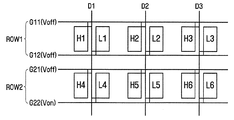
ゲートドライバ400はタイミングコントローラ600から供給されたゲート制御信号CONT1に応答して、外部から入力されるゲートオン/オフ電圧(Von、Voff)を図3に示すように複数のゲートラインG11〜Gn2に順次に出力する。
In response to a gate control signal CONT1 supplied from the
図3を参照すると、一つの画素PX行が活性化され、データ電圧の入力を受ける時間を1水平周期(以下“1H”という)とすると、“1H”の間、各画素行の第1及び第2ゲートラインが順次に活性化される。すなわち、最初の“1H”で第1区間P1の間、第1画素行ROW1の第1ゲートラインG11が活性化されて、第2区間P2の間、第1画素行ROW1の第2ゲートラインG12が活性化される。2番目の“1H”で第3区間P3の間、第2画素行ROW2の第1ゲートラインG21が活性化されて、第4区間P4の間、第2画素行ROW2の第2ゲートラインG22が活性化される。 Referring to FIG. 3, if one pixel PX row is activated and the time for receiving the input of the data voltage is one horizontal cycle (hereinafter referred to as “1H”), the first and the first pixels in each pixel row are “1H”. The second gate lines are sequentially activated. That is, the first gate line G11 of the first pixel row ROW1 is activated during the first period P1 at the first “1H”, and the second gate line G12 of the first pixel row ROW1 is activated during the second period P2. Is activated. During the third period P3 in the second “1H”, the first gate line G21 of the second pixel row ROW2 is activated, and during the fourth period P4, the second gate line G22 of the second pixel row ROW2 is activated. Activated.
一方、図1のデータドライバ500はタイミングコントローラ600から供給されたデータ制御信号CONT2に応答し、先に複数の第1サブ画像信号HDATに対応する複数の第1サブデータ電圧を各データラインD1〜Dmに印加し、次に複数の第2サブ画像信号LDATに対応する複数の第2サブデータ電圧を各データラインに印加する。データドライバ500は階調電圧生成部800から複数の第1サブ画像信号HDATに対応する複数の第1サブデータ電圧及び、複数の第2サブ画像信号LDATに対応する複数の第2サブデータ電圧の入力を受ける。
On the other hand, the
図3、図4〜図7をさらに参照してより一層具体的に説明する。
第1区間P1の間、第1画素行ROW1の第1ゲートラインG11にゲートオン電圧(Von)が印加されて、残りゲートラインG12、G21、G22にゲートオフ電圧(Voff)が印加される。データドライバ500が先に複数の第1サブデータ電圧H1、H2、H3を各データラインD1、D2、D3に印加する。したがって図4に示すように第1画素行ROW1の複数の第1サブ画素SP1に各第1サブデータ電圧H1、H2、H3が供給される。
More specific description will be given with reference to FIGS. 3 and 4 to 7.
During the first period P1, the gate-on voltage (Von) is applied to the first gate line G11 of the first pixel row ROW1, and the gate-off voltage (Voff) is applied to the remaining gate lines G12, G21, and G22. The
第2区間P2の間、第1画素行ROW1の第2ゲートラインG12にゲートオン電圧(Von)が印加されて、残りゲートラインG11、G21、G22にゲートオフ電圧(Voff)が印加される。データドライバ500が複数の第2サブデータ電圧L1、L2、L3を各データラインD1、D2、D3に印加する。したがって図5に示すように第1画素行ROW1の複数の第2サブ画素SP2に各第2サブデータ電圧L1、L2、L3が供給される。
During the second period P2, the gate-on voltage (Von) is applied to the second gate line G12 of the first pixel row ROW1, and the gate-off voltage (Voff) is applied to the remaining gate lines G11, G21, and G22. The
第3区間P3の間、第2画素行ROW2の第1ゲートラインG21にゲートオン電圧(Von)が印加されて、残りゲートラインG11、G12、G22にゲートオフ電圧(Voff)が印加される。データドライバ500が複数の第1サブデータ電圧H4、H5、H6を各データラインD1、D2、D3に印加する。したがって図6に示すように第2画素行ROW2の複数の第1サブ画素SP1に各第1サブデータ電圧H4、H5、H6が供給される。
During the third period P3, the gate-on voltage (Von) is applied to the first gate line G21 of the second pixel row ROW2, and the gate-off voltage (Voff) is applied to the remaining gate lines G11, G12, and G22. The
第4区間P4の間、第2画素行ROW2の第2ゲートラインG22にゲートオン電圧(Von)が印加されて、残りゲートラインG11、G12、G21にゲートオフ電圧(Voff)が印加される。データドライバ500が複数の第2サブデータ電圧L4、L5、L6を各データラインD1、D2、D3に印加する。したがって図7に示すように第2画素行ROW2の複数の第2サブ画素SP2に各第2サブデータ電圧L4、L5、L6が供給される。
During the fourth period P4, the gate-on voltage (Von) is applied to the second gate line G22 of the second pixel row ROW2, and the gate-off voltage (Voff) is applied to the remaining gate lines G11, G12, and G21. The
図8を参照してルックアップテーブル700に保存された第1サブ画像信号HDAT及び第2サブ画像信号LDATを説明する。 The first sub image signal HDAT and the second sub image signal LDAT stored in the lookup table 700 will be described with reference to FIG.
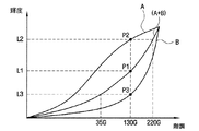
図8を参照すると、液晶パネル300に印加される階調レベル(gray scale levels)に従った輝度特性を表すガンマ曲線を示す。
液晶表示装置10の製造段階で液晶パネル300の側面視認性が最適となる第1サブ画素SP1のガンマ曲線Aと第2サブ画素PXのガンマ曲線Bを設定する。第1サブ画素PXのガンマ曲線Aと第2サブ画素PXのガンマ曲線Bは液晶表示装置10の特性及び機能に大いに依存する。
Referring to FIG. 8, a gamma curve representing a luminance characteristic according to gray scale levels applied to the
In the manufacturing stage of the liquid
液晶パネル300の第1サブ画素PXと第2サブ画素PXに同一の階調レベルに該当するデータ電圧を印加した後、液晶パネル300の正面での輝度特性を検知して、液晶パネル300の正面でのガンマ曲線(A+B)を求める。液晶パネル300の正面でのガンマ曲線(A+B)と既に設定された第1サブ画素PXのガンマ曲線Aと第2サブ画素PXのガンマ曲線Bを利用してルックアップテーブル700に第1サブ画像信号HDAT及び第2サブ画像信号LDATを保存する。
After a data voltage corresponding to the same gradation level is applied to the first sub-pixel PX and the second sub-pixel PX of the
例えば、液晶パネル300の第1サブ画素SP1と第2サブ画素SP2に同一の第1階調レベル130Gに該当するサブデータ電圧を印加すれば、液晶パネル300の正面では第1輝度L1値を有する。液晶パネル300に印加された第1階調レベル130Gと液晶パネル300から感知された第1輝度L1値が接する第1接点P1を輝度軸の方向に直線に延長して、第1サブ画素SP1のガンマ曲線Aと接する第2接点P2と第2サブ画素SP2のガンマ曲線Bと接する第3接点P3を求める。
For example, when the same sub data voltage corresponding to the
第1サブ画素SP1のガンマ曲線A上で第2接点P2は第2輝度L2値を有する。液晶パネル300の正面ガンマ曲線(A+B)上で第2輝度L2に該当する階調値は第2階調レベル220Gとなる。同様に、第2サブ画素SP2のガンマ曲線B上で第3接点P3は第3輝度L3値を有する。液晶パネル300の正面ガンマ曲線(A+B)上で第3輝度L3に該当する階調値は第3階調レベル35Gとなる。
On the gamma curve A of the first sub-pixel SP1, the second contact P2 has a second luminance L2 value. The gradation value corresponding to the second luminance L2 on the front gamma curve (A + B) of the
すなわち、液晶パネル300の正面でガンマ特性が第1接点P1として表現されるためには、第1サブ画素SP1には第2階調レベル220Gに該当するサブデータ電圧が印加されなければならず、第2サブ画素SP2には第3階調レベル35Gに該当するサブデータ電圧が印加されなければならない。
That is, in order to express the gamma characteristic as the first contact point P1 on the front surface of the
上述した方法で、外部から入力される画像信号ISIGの各階調レベルに対応して、第1及び第2サブ画素SP1、SP2に印加する第1サブデータ電圧及び第2サブデータ電圧に対応する第1サブ画像信号HDAT及び第2サブ画像信号LDATをルックアップテーブル700に保存することができる。 According to the above-described method, the first sub data voltage and the second sub data voltage applied to the first and second sub pixels SP1 and SP2 corresponding to each gradation level of the image signal ISIG input from the outside. The first sub image signal HDAT and the second sub image signal LDAT can be stored in the lookup table 700.
上述したように、側面視認性を最適化することができるよう画像信号ISIGを第1及び第2サブ画像信号HDAT、LDATに変換し、各第1及び第2サブ画素SP1、SP2に第1及び第2サブデータ電圧を供給することにより表示品質が向上される。 As described above, the image signal ISIG is converted into the first and second sub-image signals HDAT and LDAT so that the side visibility can be optimized, and the first and second sub-pixels SP1 and SP2 have the first and second sub-pixels SP1 and SP2, respectively. Display quality is improved by supplying the second sub data voltage.
一方、第1及び第2サブ画素SP1、SP2は一つのデータラインを共有するため、表示駆動部は複数の第1サブデータ電圧を先に各データラインD1〜Dmに印加し、次に複数の第2サブデータ電圧を各データラインD1〜Dmに印加しなければならない。 Meanwhile, since the first and second sub-pixels SP1 and SP2 share one data line, the display driver applies a plurality of first sub-data voltages to the data lines D1 to Dm first, and then a plurality of data lines. A second sub data voltage must be applied to each data line D1-Dm.
このため、表示駆動部が駆動動作を実行する一番目の方法としては、タイミングコントローラ600が先に複数の第1サブ画像信号HDATを各データラインD1〜Dmに供給し、その後、複数の第2サブ画像信号LDATを各データラインD1〜Dmに供給する方法がある。この時、データドライバ500はタイミングコントローラ600から順次に出力される複数の第1サブ画像信号HDATを先に複数の第1サブデータ電圧に変換して出力し、その次に複数の第2サブ画像信号LDATを複数の第2サブデータ電圧に変換して出力するものである。
Therefore, as a first method for the display driving unit to execute the driving operation, the
2番目方法としては、タイミングコントローラ600が入力される画像信号ISIGに対応する第1サブ画像信号HDATと第2サブ画像信号LDATを出力し、データドライバ500が出力された複数の第1及び第2サブ画像信号(HDAT、LDAT)のうち先に複数の第1サブ画像信号HDATを複数の第1サブデータ電圧に変換して出力し、その次に複数の第2サブ画像信号LDATを複数の第2サブデータ電圧に変換して出力するものである。
As a second method, the first sub image signal HDAT and the second sub image signal LDAT corresponding to the image signal ISIG input to the
本発明による表示装置は上記2種類の方法に限定されず、多様な方法で動作され得るが、以下では上述した1番目の方法で動作する表示装置を具体的な実施形態を通して説明する。 The display device according to the present invention is not limited to the above two types of methods, and can be operated in various ways. Hereinafter, the display device that operates in the first method described above will be described through specific embodiments.
図9及び図10を参照して本発明の一実施形態による表示装置を説明する。
図9は、本発明の一実施形態による表示装置のタイミングコントローラの概略ブロック図であり、図10は、図9のタイミングコントローラの動作を説明するための概念図である。
A display device according to an exemplary embodiment of the present invention will be described with reference to FIGS. 9 and 10.
FIG. 9 is a schematic block diagram of the timing controller of the display device according to the embodiment of the present invention, and FIG. 10 is a conceptual diagram for explaining the operation of the timing controller of FIG.
図9を参照すると、タイミングコントローラ601はメモリコントローラ610と、保存部620と出力部630を含む。
Referring to FIG. 9, the
先ず、メモリコントローラ610は、画像信号ISIGの入力を受けこれに対応する第1サブ画像信号HDAT及び第2サブ画像信号LDATをルックアップテーブル700から読み出す。ここでメモリコントローラ610は第1サブ画像信号HDAT及び第2サブ画像信号LDATを同時に読み出すことができ、あるいは順次に読み出すことができる。
First, the
保存部620は、メモリコントローラ610から出力された第1サブ画像信号HDAT及び第2サブ画像信号LDATを保存する。保存部620は一画素行の複数の第1サブ画素SP1に提供される複数の第1サブ画像信号HDATを複数の第2サブ画像信号LDATより先に出力するために複数の第1サブ画像信号HDAT及び第2サブ画像信号LDATを保存する。出力部630はメモリに保存されている複数の第1サブ画像信号HDATを先に出力し、次に複数の第2サブ画像信号LDATを出力する。
The
ここで図10をさらに参照して保存部620と出力部630の動作をさらに詳細に説明する。
以下では一画素行に4個の画素PXを含む場合を例にあげて説明する。一画素PX行は4個の第1サブ画素SP1と4個の第2サブ画素SP2を含む。
Here, the operations of the
Hereinafter, a case where four pixels PX are included in one pixel row will be described as an example. One pixel PX row includes four first sub-pixels SP1 and four second sub-pixels SP2.
先ず、時間T1において保存部620は、第1画素行の3個の第1サブ画素SP1に供給される3個の第1サブ画像信号(HDAT1_1、HDAT1_2、HDAT1_3)と3個の第2サブ画素SP2に供給される3個の第2サブ画像信号(LDAT1_1、LDAT1_2、LDAT1_3)を保存する。
First, at time T1, the
次に、メモリコントローラ610が第1画素行の4番目の画素PXに供給される第1サブ画像信号(HDAT1_4)及び第2サブ画像信号(LDAT1_4)を供給するとき、時間T2において、保存部620は第1サブ画像信号(HDAT1_4)及び第2サブ画像信号(LDAT1_4)を保存する。この時、出力部630は保存部620から第1画素行の1番目の画素PXと2番目の画素PXに供給される第1サブ画像信号(HDAT1_1、HDAT1_2)を出力する。
Next, when the
次に、メモリコントローラ610が第2画素行の1番目の画素PXに供給される第1サブ画像信号(HDAT2_1)及び第2サブ画像信号(LDAT2_1)を供給するとき、時間T3において、保存部620は第1サブ画像信号(HDAT2_1)及び第2サブ画像信号(LDAT2_1)を保存する。この時、出力部630は保存部620から第1画素行の3番目の画素PXと4番目の画素PXに供給される第1サブ画像信号(HDAT1_3、HDAT1_4)を出力する。
Next, when the
次に、メモリコントローラ610が第2画素行の2番目の画素PXに供給される第1サブ画像信号(HDAT2_2)及び第2サブ画像信号(LDAT2_2)を供給するとき、時間T4において、保存部620は第1サブ画像信号HDAT(HDAT2_2)及び第2サブ画像信号(LDAT2_2)を保存する。この時、出力部630は保存部620から第1画素行の一番目の画素PXと2番目の画素PXに供給される第2サブ画像信号(LDAT1_2、LDAT1_1)を出力する。
Next, when the
次に、メモリコントローラ610が第2画素行の3番目の画素PXに供給される第1サブ画像信号(HDAT2_3)及び第2サブ画像信号(LDAT2_3)を供給するとき、時間T5において、保存部620は第1サブ画像信号(HDAT2_3)及び第2サブ画像信号(LDAT2_3)を保存する。この時、出力部630は保存部620から第1画素行の3番目の画素PXと4番目の画素PXに供給される第2サブ画像信号(LDAT1_3、LDAT1_4)を出力する。
Next, when the
整理して説明すれば、保存部620はメモリコントローラ610から出力された複数の第1サブ画像信号HDAT及び複数の第2サブ画像信号LDATを保存し、出力部630が保存部620から一画素PX行に対する複数の第1サブ画像信号HDATを先に出力し、次に一画素PX行に対する複数の第2サブ画像信号LDATを出力する。
For example, the
図11及び図12を参照し、本発明の他の実施形態による表示装置及びその駆動方法を説明する。
図11は、本発明の他の実施形態による表示装置のタイミングコントローラのブロック図であり、図12は、図11のタイミングコントローラの動作を説明するための概念図である。
図9に示した構成要素と同一の機能をする構成要素に対しては同一の図面符号を使用し、説明の便宜上、該当構成要素の詳細な説明は省略する。
A display device and a driving method thereof according to another embodiment of the present invention will be described with reference to FIGS. 11 and 12.
11 is a block diagram of a timing controller of a display device according to another embodiment of the present invention, and FIG. 12 is a conceptual diagram for explaining the operation of the timing controller of FIG.
Components having the same functions as those shown in FIG. 9 are denoted by the same reference numerals, and detailed description of the corresponding components is omitted for convenience of description.
図11を参照すると、タイミングコントローラ602は保存部640とメモリコントローラ650を含む。
Referring to FIG. 11, the
保存部640は画像信号ISIGの入力を受け保存する。メモリコントローラ650は保存部640に保存された画像信号ISIGの入力を受けこれに対応する複数の第1サブ画像信号HDATを先に読み出して出力し、次に複数の第2サブ画像信号LDATを読み出して出力する。
The
図12をさらに参照して保存部640とメモリコントローラ650の動作をさらに詳細に説明する。
以下では一画素行に4個の画素PXを含む場合を例にあげて説明する。一画素行は4個の第1サブ画素SP1と4個の第2サブ画素SP2を含む。
The operations of the
Hereinafter, a case where four pixels PX are included in one pixel row will be described as an example. One pixel row includes four first sub-pixels SP1 and four second sub-pixels SP2.
まず、時間T1において、保存部640は第1画素行の3個の画素PXに供給される3個の画像信号(ISIG1_1、ISIG1_2、ISIG1_3)を保存する。
First, at time T1, the
時間T2において、保存部640は第1画素行の4番目の画素PXに供給される画像信号(ISIG1_4)を保存する。この時、メモリコントローラ650は先に第1画素行の一番目の画素PXに供給される画像信号(ISIG1_1)の入力を受けこれに対応する第1サブ画像信号(HDAT1_1)をルックアップテーブル700から読み出して出力する。次に、第1画素行の2番目の画素PXに供給される画像信号(ISIG1_2)の入力を受けこれに対応する第1サブ画像信号(HDAT1_2)をルックアップテーブル700から読み出して出力する。
At time T2, the
時間T3において、保存部640が第2画素行の一番目の画素PXに供給される画像信号(ISIG2_1)を保存する。この時、メモリコントローラ650は先に第1画素行の3番目の画素PXに供給される画像信号(ISIG1_3)の入力を受けこれに対応する第1サブ画像信号(HDAT1_3)をルックアップテーブル700から読み出して出力する。次に、第1画素行の4番目の画素PXに供給される画像信号(ISIG1_4)の入力を受けこれに対応する第1サブ画像信号(HDAT1_4)をルックアップテーブル700から読み出して出力する
At time T3, the
時間T4において、保存部640が第2画素行の2番目の画素PXに供給される画像信号(ISIG2_2)を保存する。この時、メモリコントローラ650は先に第1画素行の一番目の画素PXに供給される画像信号(ISIG1_1)の入力を受けこれに対応する第2サブ画像信号(LDAT1_1)をルックアップテーブル700から読み出して出力する。次に、第1画素行の2番目の画素PXに供給される画像信号(ISIG1_2)の入力を受けこれに対応する第2サブ画像信号(LDAT1_2)をルックアップテーブル700から読み出して出力する。
At time T4, the
時間T5において、保存部640が第2画素行の3番目の画素PXに供給される画像信号(ISIG2_3)を保存する。この時、メモリコントローラ650は先に第1画素行の3番目の画素PXに供給される画像信号(ISIG1_3)の入力を受けこれに対応する第2サブ画像信号(LDAT1_3)をルックアップテーブル700から読み出して出力する。次に、第1画素行の4番目の画素PXに供給される画像信号(ISIG1_4)の入力を受けこれに対応する第2サブ画像信号(LDAT1_4)をルックアップテーブル700から読み出して出力する。
At time T5, the
以上を整理して説明すれば、保存部640は画像信号ISIGを保存して、メモリコントローラ650が一画素行に対する画像信号ISIGに対応する複数の第1サブ画像信号HDATを先に読み出して出力し、次に一画素行に対する複数の第2サブ画像信号LDATを読み出して出力する。
To explain the above, the
尚、本発明は、上述の実施例に限られるものではない。本発明の技術的範囲から逸脱しない範囲内で多様に変更実施することが可能である。 The present invention is not limited to the above-described embodiments. Various modifications can be made without departing from the technical scope of the present invention.
本発明は、液晶表示装置などのフラットパネル表示装置に利用される。 The present invention is used in a flat panel display device such as a liquid crystal display device.
10 液晶表示装置
100 第1基板
200 第2基板
300 液晶パネル
400 ゲートドライバ
500 データドライバ
600、601、602 タイミングコントローラ
610、650 メモリコントローラ
620、640 保存部
630 出力部
700 ルックアップテーブル
800 階調電圧生成部
DESCRIPTION OF
Claims (19)
画像信号の入力を受け、前記画像信号を第1サブ画像信号と第2サブ画像信号に変換し、第1サブデータ電圧を前記データラインを通して前記第1サブ画素に供給し、前記第1サブデータ電圧を供給した後に第2サブデータ電圧を前記データラインを通して前記第2サブ画素に供給する表示駆動部とを有し、
前記第1サブデータ電圧は前記第1サブ画像信号に対応し、前記第2サブデータ電圧は前記第2サブ画像信号に対応することを特徴とする表示装置。 A display panel including a plurality of pixels and displaying an image, wherein each pixel includes a data line, first and second gate lines, and a first sub-pixel connected to the data line and the first gate line. A display panel including a second sub-pixel connected to the data line and the second gate line;
Receiving an input of an image signal, converting the image signal into a first sub-image signal and a second sub-image signal, and supplying a first sub-data voltage to the first sub-pixel through the data line; A display driver for supplying a second sub data voltage to the second sub pixel through the data line after supplying a voltage;
The display device according to claim 1, wherein the first sub data voltage corresponds to the first sub image signal, and the second sub data voltage corresponds to the second sub image signal.
読み出された前記第1及び第2サブ画像信号に対応する前記第1及び第2サブデータ電圧を供給するデータドライバとを含むことを特徴とする請求項4に記載の表示装置。 The display driving unit reads the first and second sub image signals corresponding to the image signal from the lookup table, and sequentially outputs the timing controller;
The display device according to claim 4, further comprising a data driver that supplies the first and second sub data voltages corresponding to the read first and second sub image signals.
複数の画像信号の入力を受け、前記各画像信号を複数の第1サブ画像信号と第2サブ画像信号に変換し、前記複数の第1サブ画像信号に対応する複数の第1サブデータ電圧を前記第i画素行の前記複数の第1サブ画素に供給し、前記複数の第1サブデータ電圧を供給した後に前記複数の第2サブ画像信号に対応する複数の第2サブデータ電圧を前記第i画素行の前記複数の第2サブ画素に供給する表示駆動部とを有することを特徴とする表示装置。 A display panel including a first pixel row to an n-th (n is an integer greater than 1) pixel row, wherein the i-th (1 ≦ i ≦ n) pixel row includes a plurality of pixels, and each pixel includes a first sub-row. A display panel including a pixel and a second sub-pixel;
Receiving a plurality of image signals, converting each of the image signals into a plurality of first sub-image signals and second sub-image signals, and generating a plurality of first sub-data voltages corresponding to the plurality of first sub-image signals; Supplying a plurality of second sub data voltages corresponding to the plurality of second sub image signals after supplying the plurality of first sub data voltages to the plurality of first sub pixels of the i-th pixel row; and a display driver for supplying the plurality of second sub-pixels in the i-pixel row.
前記複数の第1サブ画像信号を出力し、
前記複数の第1サブ画像信号を出力した後に前記複数の第2サブ画像信号を出力することを特徴とする請求項8に記載の表示装置。 The display driving unit reads the plurality of first and second sub image signals corresponding to the plurality of image signals from a lookup table,
Outputting the plurality of first sub-image signals;
The display device according to claim 8, wherein the plurality of second sub image signals are output after the plurality of first sub image signals are output.
読み出された複数の第1及び第2サブ画像信号を保存する保存部と、
前記保存部に保存された複数の第1サブ画像信号を出力し、前記複数の第1サブ画像信号を出力した後に前記保存部に保存された複数の第2サブ画像信号を出力する出力部と、
前記出力部から出力された複数の第1サブ画像信号及び前記複数の第2サブ画像信号を前記複数の第1サブデータ電圧及び前記複数の第2サブデータ電圧に変換して、各々前記複数の第1サブ画素及び第2サブ画素に供給するデータドライバとを含むことを特徴とする請求項9に記載の表示装置。 The display driving unit reads a plurality of the first and second sub image signals corresponding to the plurality of image signals from the lookup table;
A storage unit for storing the read first and second sub-image signals;
An output unit that outputs a plurality of first sub image signals stored in the storage unit, outputs a plurality of second sub image signals stored in the storage unit after outputting the plurality of first sub image signals; ,
The plurality of first sub image signals and the plurality of second sub image signals output from the output unit are converted into the plurality of first sub data voltages and the plurality of second sub data voltages, respectively. The display device according to claim 9, further comprising a data driver that supplies the first sub-pixel and the second sub-pixel.
前記第1サブ画像信号を読み出して出力した後に前記複数の画像信号に対応する前記複数の第2サブ画像信号を前記ルックアップテーブルから読み出して出力することを特徴とする請求項8に記載の表示装置。 The display driving unit reads and outputs the plurality of first sub-image signals corresponding to the plurality of image signals from the lookup table,
9. The display according to claim 8, wherein after the first sub image signal is read and output, the plurality of second sub image signals corresponding to the plurality of image signals are read from the look-up table and output. apparatus.
前記保存部に保存された複数の画像信号に対応する前記複数の第1サブ画像信号を前記ルックアップテーブルから読み出して出力し、前記複数の第1サブ画像信号を出力した後に前記保存部に保存された複数の画像信号に対応する前記複数の第2サブ画像信号を前記ルックアップテーブルから読み出して出力するメモリコントローラと、
前記メモリコントローラから出力された複数の第1サブ画像信号及び前記複数の第2サブ画像信号を前記複数の第1サブデータ電圧及び前記複数の第2サブデータ電圧に変換して各々前記複数の第1サブ画素及び第2サブ画素に供給するデータドライバとを含むことを特徴とする請求項11に記載の表示装置。 The display driving unit includes a storage unit that stores the plurality of image signals;
The plurality of first sub image signals corresponding to the plurality of image signals stored in the storage unit are read out from the lookup table and output, and the plurality of first sub image signals are output and then stored in the storage unit A memory controller that reads out and outputs the plurality of second sub-image signals corresponding to the plurality of image signals,
The plurality of first sub image signals and the plurality of second sub image signals output from the memory controller are converted into the plurality of first sub data voltages and the plurality of second sub data voltages, respectively. The display device according to claim 11, further comprising a data driver that supplies the first sub-pixel and the second sub-pixel.
前記各第2サブ画素と接続される第2ゲートラインと、
前記各第1サブ画素及び前記各第2サブ画素と接続される複数のデータラインとを含むことを特徴とする請求項7に記載の表示装置。 Each pixel row includes a first gate line connected to each first sub-pixel;
A second gate line connected to each of the second sub-pixels;
The display device of claim 7, further comprising a plurality of data lines connected to the first sub-pixels and the second sub-pixels.
複数の画像信号の入力を受信する段階と、
前記複数の画像信号を複数の第1サブ画像信号と第2サブ画像信号に変換する段階と、
前記複数の第1サブ画像信号に対応する複数の第1サブデータ電圧を前記第i画素行の前記複数の第1サブ画素に供給する段階と、
前記複数の第1サブデータ電圧を供給した後に前記複数の第2サブ画像信号に対応する複数の第2サブデータ電圧を前記第i画素行の前記複数の第2サブ画素に供給する段階とを有することを特徴とする表示装置の駆動方法。 The first pixel row to the n-th pixel row (n is an integer greater than 1) are included, and the i-th (1 ≦ i ≦ n) pixel row includes a plurality of pixels, and each pixel includes a first sub-pixel and a second sub-pixel. A driving method of a display device including pixels,
Receiving input of a plurality of image signals;
Converting the plurality of image signals into a plurality of first sub-image signals and second sub-image signals;
Supplying a plurality of first sub-data voltages corresponding to the plurality of first sub-image signals to the plurality of first sub-pixels in the i-th pixel row;
Supplying a plurality of second sub-data voltages corresponding to the plurality of second sub-image signals to the plurality of second sub-pixels in the i-th pixel row after supplying the plurality of first sub-data voltages. A display device driving method comprising:
前記複数の第1サブ画像信号を出力する段階と、
前記複数の第1サブ画像信号を出力した後に前記複数の第2サブ画像信号を出力する段階とを含むことを特徴とする請求項16に記載の表示装置の駆動方法。 Converting the first and second sub-image signals into a plurality of first and second sub-image signals corresponding to the plurality of image signals from a lookup table;
Outputting the plurality of first sub-image signals;
The method for driving a display device according to claim 16, further comprising: outputting the plurality of second sub image signals after outputting the plurality of first sub image signals.
前記第1サブ画像信号を読み出して出力した後に前記複数の画像信号に対応する複数の前記第2サブ画像信号を前記ルックアップテーブルから読み出して出力する段階とを含むことを特徴とする請求項16に記載の表示装置の駆動方法。 Converting the first and second sub-image signals into a plurality of first sub-image signals corresponding to the plurality of image signals from a lookup table and outputting them;
The method includes: reading and outputting a plurality of second sub image signals corresponding to the plurality of image signals from the lookup table after reading and outputting the first sub image signals. A driving method of the display device according to the above.
The gradation level of the first sub image signal is greater than or equal to the gradation level of the image signal, and the gradation level of the second sub image signal is less than or equal to the gradation level of the image signal. 17. The display device driving method according to claim 16, wherein the display device driving method is provided.
Applications Claiming Priority (1)
| Application Number | Priority Date | Filing Date | Title |
|---|---|---|---|
| KR1020080005080A KR20090079108A (en) | 2008-01-16 | 2008-01-16 | Display device and driving method of the same |
Publications (2)
| Publication Number | Publication Date |
|---|---|
| JP2009169398A true JP2009169398A (en) | 2009-07-30 |
| JP2009169398A5 JP2009169398A5 (en) | 2011-09-22 |
Family
ID=40451199
Family Applications (1)
| Application Number | Title | Priority Date | Filing Date |
|---|---|---|---|
| JP2008293344A Pending JP2009169398A (en) | 2008-01-16 | 2008-11-17 | Display device and method of driving the same |
Country Status (6)
| Country | Link |
|---|---|
| US (1) | US8144163B2 (en) |
| EP (1) | EP2081181A3 (en) |
| JP (1) | JP2009169398A (en) |
| KR (1) | KR20090079108A (en) |
| CN (1) | CN101488311A (en) |
| TW (1) | TWI451375B (en) |
Cited By (2)
| Publication number | Priority date | Publication date | Assignee | Title |
|---|---|---|---|---|
| WO2012063696A1 (en) * | 2010-11-10 | 2012-05-18 | シャープ株式会社 | Liquid-crystal display device |
| US9568792B2 (en) | 2013-02-05 | 2017-02-14 | Samsung Display Co., Ltd. | Liquid crystal display |
Families Citing this family (9)
| Publication number | Priority date | Publication date | Assignee | Title |
|---|---|---|---|---|
| KR101783975B1 (en) * | 2010-07-14 | 2017-10-11 | 삼성디스플레이 주식회사 | Three dimensional image display device |
| TWI411992B (en) * | 2010-12-14 | 2013-10-11 | Au Optronics Corp | Driving method of display apparatus and display apparatus |
| KR102011985B1 (en) * | 2012-07-23 | 2019-08-20 | 삼성디스플레이 주식회사 | Display device and driving method thereof |
| CN103293809B (en) * | 2013-05-28 | 2015-09-30 | 深圳市华星光电技术有限公司 | Anti-colour cast display panel |
| KR102097025B1 (en) | 2013-08-19 | 2020-04-06 | 삼성디스플레이 주식회사 | Display device and driving method thereof |
| KR102128970B1 (en) | 2013-12-18 | 2020-07-02 | 삼성디스플레이 주식회사 | Liquid crystal display |
| TW201533726A (en) * | 2014-02-17 | 2015-09-01 | Au Optronics Corp | Image display method of half-source-driving liquid crystal display |
| CN104992688B (en) * | 2015-08-05 | 2018-01-09 | 京东方科技集团股份有限公司 | Pel array, display device and its driving method and drive device |
| CN105204256B (en) * | 2015-10-29 | 2018-10-19 | 深圳市华星光电技术有限公司 | A kind of array substrate and its display device based on data line common technology |
Citations (4)
| Publication number | Priority date | Publication date | Assignee | Title |
|---|---|---|---|---|
| JP2006139288A (en) * | 2004-11-12 | 2006-06-01 | Samsung Electronics Co Ltd | Display apparatus and driving method thereof |
| JP2007086791A (en) * | 2005-09-23 | 2007-04-05 | Samsung Electronics Co Ltd | Liquid crystal panel, method for driving the same, and liquid crystal display apparatus using the same |
| JP2007164195A (en) * | 2005-12-14 | 2007-06-28 | Samsung Electronics Co Ltd | Liquid crystal display device, image signal correction method thereof, and driving method thereof |
| JP2009145601A (en) * | 2007-12-13 | 2009-07-02 | Nec Electronics Corp | Liquid crystal display device, data driver ic and method for driving liquid crystal display panel |
Family Cites Families (12)
| Publication number | Priority date | Publication date | Assignee | Title |
|---|---|---|---|---|
| US6040812A (en) * | 1996-06-19 | 2000-03-21 | Xerox Corporation | Active matrix display with integrated drive circuitry |
| KR100890025B1 (en) * | 2002-12-04 | 2009-03-25 | 삼성전자주식회사 | Liquid crystal display and apparatus and method of driving liquid crystal display |
| KR20060111148A (en) * | 2005-04-22 | 2006-10-26 | 삼성전자주식회사 | Driving apparatus of display device and driving method thereof |
| KR20060116443A (en) * | 2005-05-10 | 2006-11-15 | 삼성전자주식회사 | Display device, apparatus and method for driving thereof |
| JP4824387B2 (en) * | 2005-10-28 | 2011-11-30 | ルネサスエレクトロニクス株式会社 | LCD driver circuit |
| KR101246756B1 (en) * | 2006-02-03 | 2013-03-26 | 삼성디스플레이 주식회사 | Liquid crystal display and method of manufacturing the same |
| KR101256011B1 (en) * | 2006-04-17 | 2013-04-18 | 삼성디스플레이 주식회사 | Driving device and display apparatus having the same |
| KR101226217B1 (en) | 2006-06-15 | 2013-02-07 | 삼성디스플레이 주식회사 | Signal processing device and liquid crystal display comprising the same |
| JP5376774B2 (en) * | 2006-07-21 | 2013-12-25 | 三星ディスプレイ株式會社 | Liquid crystal display |
| CN100516998C (en) * | 2006-11-17 | 2009-07-22 | 群康科技(深圳)有限公司 | Liquid crystal display device and its driving method |
| KR20080056493A (en) * | 2006-12-18 | 2008-06-23 | 삼성전자주식회사 | Thin film transistor substrate and method of manufacturing the same |
| KR101335424B1 (en) * | 2006-12-29 | 2013-12-02 | 엘지디스플레이 주식회사 | driving method of a built in image sensor for liquid crystal display device |
-
2008
- 2008-01-16 KR KR1020080005080A patent/KR20090079108A/en not_active Application Discontinuation
- 2008-10-30 US US12/261,507 patent/US8144163B2/en active Active
- 2008-11-17 JP JP2008293344A patent/JP2009169398A/en active Pending
- 2008-12-31 EP EP08022588A patent/EP2081181A3/en not_active Ceased
-
2009
- 2009-01-05 TW TW098100049A patent/TWI451375B/en not_active IP Right Cessation
- 2009-01-06 CN CNA2009100001145A patent/CN101488311A/en active Pending
Patent Citations (4)
| Publication number | Priority date | Publication date | Assignee | Title |
|---|---|---|---|---|
| JP2006139288A (en) * | 2004-11-12 | 2006-06-01 | Samsung Electronics Co Ltd | Display apparatus and driving method thereof |
| JP2007086791A (en) * | 2005-09-23 | 2007-04-05 | Samsung Electronics Co Ltd | Liquid crystal panel, method for driving the same, and liquid crystal display apparatus using the same |
| JP2007164195A (en) * | 2005-12-14 | 2007-06-28 | Samsung Electronics Co Ltd | Liquid crystal display device, image signal correction method thereof, and driving method thereof |
| JP2009145601A (en) * | 2007-12-13 | 2009-07-02 | Nec Electronics Corp | Liquid crystal display device, data driver ic and method for driving liquid crystal display panel |
Cited By (3)
| Publication number | Priority date | Publication date | Assignee | Title |
|---|---|---|---|---|
| WO2012063696A1 (en) * | 2010-11-10 | 2012-05-18 | シャープ株式会社 | Liquid-crystal display device |
| US9568792B2 (en) | 2013-02-05 | 2017-02-14 | Samsung Display Co., Ltd. | Liquid crystal display |
| US10146097B2 (en) | 2013-02-05 | 2018-12-04 | Samsung Display Co., Ltd. | Liquid crystal display |
Also Published As
| Publication number | Publication date |
|---|---|
| US8144163B2 (en) | 2012-03-27 |
| US20090179906A1 (en) | 2009-07-16 |
| TW200947383A (en) | 2009-11-16 |
| EP2081181A3 (en) | 2010-12-15 |
| TWI451375B (en) | 2014-09-01 |
| KR20090079108A (en) | 2009-07-21 |
| EP2081181A2 (en) | 2009-07-22 |
| CN101488311A (en) | 2009-07-22 |
Similar Documents
| Publication | Publication Date | Title |
|---|---|---|
| JP2009169398A (en) | Display device and method of driving the same | |
| US10733951B2 (en) | Display device and driving method thereof | |
| KR102437170B1 (en) | Gate driver and Flat Panel Display Device including the same | |
| US9269329B2 (en) | Display device, data processor and method thereof | |
| US9052538B2 (en) | Liquid crystal display device | |
| KR20140042983A (en) | Liquid crystal display device | |
| JP2006058891A (en) | Display apparatus, its drive unit and driving method | |
| KR20080109512A (en) | Display apparatus and method of driving the same | |
| JP2008197228A (en) | Display device | |
| JP2009139774A (en) | Display device | |
| KR20100056228A (en) | Liquid crystal display and driving method of the same | |
| JP2009169398A5 (en) | ||
| US20120249507A1 (en) | Driving apparatus and driving method of display device | |
| CN101661719B (en) | Black frame inserting method for liquid crystal display | |
| KR20160086436A (en) | Gate shift register and display device using the same | |
| JP4783154B2 (en) | Flat display device and driving method thereof | |
| JP2009288666A (en) | Display device | |
| KR20110078711A (en) | Liquid crystal display device | |
| JP2007334305A (en) | Signal processing device and liquid crystal display apparatus having the same | |
| KR20080017626A (en) | Liquid display device | |
| KR20150070683A (en) | Liquid display device and driving method for the same | |
| KR101872481B1 (en) | Liquid crystal display device and method of driving the same | |
| KR102552303B1 (en) | Display device and driving mathod thereof | |
| KR20070065063A (en) | Method for driving data line and flat penal display using the same | |
| JP2020056924A (en) | Display |
Legal Events
| Date | Code | Title | Description |
|---|---|---|---|
| A521 | Written amendment |
Free format text: JAPANESE INTERMEDIATE CODE: A523 Effective date: 20110805 |
|
| A621 | Written request for application examination |
Free format text: JAPANESE INTERMEDIATE CODE: A621 Effective date: 20110805 |
|
| A521 | Written amendment |
Free format text: JAPANESE INTERMEDIATE CODE: A523 Effective date: 20120705 |
|
| A131 | Notification of reasons for refusal |
Free format text: JAPANESE INTERMEDIATE CODE: A131 Effective date: 20121127 |
|
| A977 | Report on retrieval |
Free format text: JAPANESE INTERMEDIATE CODE: A971007 Effective date: 20121128 |
|
| A711 | Notification of change in applicant |
Free format text: JAPANESE INTERMEDIATE CODE: A712 Effective date: 20121213 |
|
| A601 | Written request for extension of time |
Free format text: JAPANESE INTERMEDIATE CODE: A601 Effective date: 20130227 |
|
| A602 | Written permission of extension of time |
Free format text: JAPANESE INTERMEDIATE CODE: A602 Effective date: 20130304 |
|
| A521 | Written amendment |
Free format text: JAPANESE INTERMEDIATE CODE: A523 Effective date: 20130327 |
|
| A02 | Decision of refusal |
Free format text: JAPANESE INTERMEDIATE CODE: A02 Effective date: 20130423 |
|
| A521 | Written amendment |
Free format text: JAPANESE INTERMEDIATE CODE: A523 Effective date: 20130822 |
|
| A911 | Transfer of reconsideration by examiner before appeal (zenchi) |
Free format text: JAPANESE INTERMEDIATE CODE: A911 Effective date: 20130829 |
|
| A912 | Removal of reconsideration by examiner before appeal (zenchi) |
Free format text: JAPANESE INTERMEDIATE CODE: A912 Effective date: 20130920 |