KR20090079108A - Display device and driving method of the same - Google Patents
Display device and driving method of the same Download PDFInfo
- Publication number
- KR20090079108A KR20090079108A KR1020080005080A KR20080005080A KR20090079108A KR 20090079108 A KR20090079108 A KR 20090079108A KR 1020080005080 A KR1020080005080 A KR 1020080005080A KR 20080005080 A KR20080005080 A KR 20080005080A KR 20090079108 A KR20090079108 A KR 20090079108A
- Authority
- KR
- South Korea
- Prior art keywords
- sub
- image signals
- pixel
- image signal
- sub image
- Prior art date
Links
Images


Classifications
-
- G—PHYSICS
- G09—EDUCATION; CRYPTOGRAPHY; DISPLAY; ADVERTISING; SEALS
- G09G—ARRANGEMENTS OR CIRCUITS FOR CONTROL OF INDICATING DEVICES USING STATIC MEANS TO PRESENT VARIABLE INFORMATION
- G09G3/00—Control arrangements or circuits, of interest only in connection with visual indicators other than cathode-ray tubes
- G09G3/20—Control arrangements or circuits, of interest only in connection with visual indicators other than cathode-ray tubes for presentation of an assembly of a number of characters, e.g. a page, by composing the assembly by combination of individual elements arranged in a matrix no fixed position being assigned to or needed to be assigned to the individual characters or partial characters
- G09G3/34—Control arrangements or circuits, of interest only in connection with visual indicators other than cathode-ray tubes for presentation of an assembly of a number of characters, e.g. a page, by composing the assembly by combination of individual elements arranged in a matrix no fixed position being assigned to or needed to be assigned to the individual characters or partial characters by control of light from an independent source
- G09G3/36—Control arrangements or circuits, of interest only in connection with visual indicators other than cathode-ray tubes for presentation of an assembly of a number of characters, e.g. a page, by composing the assembly by combination of individual elements arranged in a matrix no fixed position being assigned to or needed to be assigned to the individual characters or partial characters by control of light from an independent source using liquid crystals
- G09G3/3611—Control of matrices with row and column drivers
- G09G3/3648—Control of matrices with row and column drivers using an active matrix
-
- G—PHYSICS
- G02—OPTICS
- G02F—OPTICAL DEVICES OR ARRANGEMENTS FOR THE CONTROL OF LIGHT BY MODIFICATION OF THE OPTICAL PROPERTIES OF THE MEDIA OF THE ELEMENTS INVOLVED THEREIN; NON-LINEAR OPTICS; FREQUENCY-CHANGING OF LIGHT; OPTICAL LOGIC ELEMENTS; OPTICAL ANALOGUE/DIGITAL CONVERTERS
- G02F1/00—Devices or arrangements for the control of the intensity, colour, phase, polarisation or direction of light arriving from an independent light source, e.g. switching, gating or modulating; Non-linear optics
- G02F1/01—Devices or arrangements for the control of the intensity, colour, phase, polarisation or direction of light arriving from an independent light source, e.g. switching, gating or modulating; Non-linear optics for the control of the intensity, phase, polarisation or colour
- G02F1/13—Devices or arrangements for the control of the intensity, colour, phase, polarisation or direction of light arriving from an independent light source, e.g. switching, gating or modulating; Non-linear optics for the control of the intensity, phase, polarisation or colour based on liquid crystals, e.g. single liquid crystal display cells
- G02F1/133—Constructional arrangements; Operation of liquid crystal cells; Circuit arrangements
-
- G—PHYSICS
- G09—EDUCATION; CRYPTOGRAPHY; DISPLAY; ADVERTISING; SEALS
- G09G—ARRANGEMENTS OR CIRCUITS FOR CONTROL OF INDICATING DEVICES USING STATIC MEANS TO PRESENT VARIABLE INFORMATION
- G09G3/00—Control arrangements or circuits, of interest only in connection with visual indicators other than cathode-ray tubes
- G09G3/20—Control arrangements or circuits, of interest only in connection with visual indicators other than cathode-ray tubes for presentation of an assembly of a number of characters, e.g. a page, by composing the assembly by combination of individual elements arranged in a matrix no fixed position being assigned to or needed to be assigned to the individual characters or partial characters
- G09G3/34—Control arrangements or circuits, of interest only in connection with visual indicators other than cathode-ray tubes for presentation of an assembly of a number of characters, e.g. a page, by composing the assembly by combination of individual elements arranged in a matrix no fixed position being assigned to or needed to be assigned to the individual characters or partial characters by control of light from an independent source
- G09G3/36—Control arrangements or circuits, of interest only in connection with visual indicators other than cathode-ray tubes for presentation of an assembly of a number of characters, e.g. a page, by composing the assembly by combination of individual elements arranged in a matrix no fixed position being assigned to or needed to be assigned to the individual characters or partial characters by control of light from an independent source using liquid crystals
- G09G3/3611—Control of matrices with row and column drivers
- G09G3/3685—Details of drivers for data electrodes
-
- G—PHYSICS
- G09—EDUCATION; CRYPTOGRAPHY; DISPLAY; ADVERTISING; SEALS
- G09G—ARRANGEMENTS OR CIRCUITS FOR CONTROL OF INDICATING DEVICES USING STATIC MEANS TO PRESENT VARIABLE INFORMATION
- G09G2300/00—Aspects of the constitution of display devices
- G09G2300/04—Structural and physical details of display devices
- G09G2300/0439—Pixel structures
- G09G2300/0443—Pixel structures with several sub-pixels for the same colour in a pixel, not specifically used to display gradations
- G09G2300/0447—Pixel structures with several sub-pixels for the same colour in a pixel, not specifically used to display gradations for multi-domain technique to improve the viewing angle in a liquid crystal display, such as multi-vertical alignment [MVA]
-
- G—PHYSICS
- G09—EDUCATION; CRYPTOGRAPHY; DISPLAY; ADVERTISING; SEALS
- G09G—ARRANGEMENTS OR CIRCUITS FOR CONTROL OF INDICATING DEVICES USING STATIC MEANS TO PRESENT VARIABLE INFORMATION
- G09G2310/00—Command of the display device
- G09G2310/02—Addressing, scanning or driving the display screen or processing steps related thereto
- G09G2310/0262—The addressing of the pixel, in a display other than an active matrix LCD, involving the control of two or more scan electrodes or two or more data electrodes, e.g. pixel voltage dependent on signals of two data electrodes
-
- G—PHYSICS
- G09—EDUCATION; CRYPTOGRAPHY; DISPLAY; ADVERTISING; SEALS
- G09G—ARRANGEMENTS OR CIRCUITS FOR CONTROL OF INDICATING DEVICES USING STATIC MEANS TO PRESENT VARIABLE INFORMATION
- G09G2320/00—Control of display operating conditions
- G09G2320/02—Improving the quality of display appearance
- G09G2320/028—Improving the quality of display appearance by changing the viewing angle properties, e.g. widening the viewing angle, adapting the viewing angle to the view direction
-
- G—PHYSICS
- G09—EDUCATION; CRYPTOGRAPHY; DISPLAY; ADVERTISING; SEALS
- G09G—ARRANGEMENTS OR CIRCUITS FOR CONTROL OF INDICATING DEVICES USING STATIC MEANS TO PRESENT VARIABLE INFORMATION
- G09G2320/00—Control of display operating conditions
- G09G2320/06—Adjustment of display parameters
- G09G2320/0673—Adjustment of display parameters for control of gamma adjustment, e.g. selecting another gamma curve
Landscapes
- Engineering & Computer Science (AREA)
- Physics & Mathematics (AREA)
- General Physics & Mathematics (AREA)
- Theoretical Computer Science (AREA)
- Computer Hardware Design (AREA)
- Crystallography & Structural Chemistry (AREA)
- Chemical & Material Sciences (AREA)
- Nonlinear Science (AREA)
- Mathematical Physics (AREA)
- Optics & Photonics (AREA)
- Control Of Indicators Other Than Cathode Ray Tubes (AREA)
- Liquid Crystal (AREA)
- Liquid Crystal Display Device Control (AREA)
Abstract
Description
본 발명은 표시 장치 및 그의 구동 방법에 관한 것이다.The present invention relates to a display device and a driving method thereof.
평판 표시 장치의 일 예인 액정 표시 장치는 시야각(viewing angle)이 좁다는 단점을 갖는데, 이를 개선하기 위해, 광시야각 특성을 갖는 PVA(Patterned Vertical Alignment) 모드, MVA(Multi-domain Vertical Alignment) 모드 및 S-PVA(Super-Patterned Vertical Alignment) 모드의 액정 표시 장치가 개발되고 있다.A liquid crystal display, which is an example of a flat panel display, has a disadvantage of having a narrow viewing angle. To improve this, a liquid crystal display includes a patterned vertical alignment (PVA) mode, a multi-domain vertical alignment (MVA) mode, and a wide viewing angle. A liquid crystal display device having a super-patterned vertical alignment (S-PVA) mode has been developed.
특히 S-PVA 모드 액정 표시 장치는 두 개의 서브 화소로 이루어진 화소를 구비한다. 각 서브 화소에는 서로 다른 서브 데이터 전압이 인가되어 각 서브 화소마다 빛의 투과율이 다르게 되고, 두 서브 화소를 포함하는 하나의 화소는 서로 다른 두 투과율의 중간값으로 보여진다. 이러한 S-PVA 모드를 통해 액정 표시 장치의 측면 시야각을 넓힐 수 있다.In particular, the S-PVA mode liquid crystal display includes a pixel consisting of two sub-pixels. Different sub data voltages are applied to each sub pixel so that light transmittance is different for each sub pixel, and one pixel including two sub pixels is regarded as an intermediate value of two different transmittances. Through the S-PVA mode, the side viewing angle of the liquid crystal display may be widened.
그러나 종래에는 두 서브 화소에 제공되는 서브 데이터 전압을 각각 개별적으로 제어할 수 없었다. 그로 인해 표시 품질을 더욱 향상시킬 수 없었다. 이에 본 발명이 이루고자 하는 기술적 과제는 표시 품질을 향상시킬 수 있는 표시 장치를 제공하는 것이다.However, conventionally, the sub data voltages provided to the two sub pixels cannot be individually controlled. As a result, the display quality could not be further improved. Accordingly, an aspect of the present invention is to provide a display device capable of improving display quality.
본 발명이 이루고자 하는 다른 기술적 과제는 표시 품질을 향상시킬 수 있는 표시 장치의 구동 방법을 제공하는 것이다.Another object of the present invention is to provide a method of driving a display device capable of improving display quality.
본 발명의 기술적 과제는 이상에서 언급한 기술적 과제들로 제한되지 않으며, 언급되지 않은 또 다른 기술적 과제들은 아래의 기재로부터 당업자에게 명확하게 이해될 수 있을 것이다. The technical problem of the present invention is not limited to the technical problems mentioned above, and other technical problems not mentioned will be clearly understood by those skilled in the art from the following description.
상기 기술적 과제를 달성하기 위한 본 발명의 일 태양에 따른 표시 장치는, 다수의 화소를 포함하여 영상을 표시하는 표시 패널로서, 상기 각 화소는 데이터 라인과, 제1 및 제2 게이트 라인과, 상기 데이터 라인 및 상기 제1 게이트 라인에 연결된 제1 서브 화소와, 상기 데이터 라인 및 상기 제2 게이트 라인에 연결된 제2 서브 화소를 포함하는 표시 패널 및 영상 신호를 입력받고, 상기 영상 신호를 제1 서브 영상 신호와 제2 서브 영상 신호로 변환하고, 제1 서브 데이터 전압을 상기 데이터 라인을 통해 상기 제1 화소에 제공하고, 상기 제1 서브 데이터 전압을 제공한 후에 제2 서브 데이터 전압을 상기 데이터 라인을 통해 상기 제2 서브 화소로 제공하는 표시 구동부로서, 상기 제1 서브 데이터 전압은 상기 제1 서브 영상 신호에 대응하고, 상기 제2 서브 데이터 전압은 상기 제2 서브 영상 신호에 대응하는 표시 구동부를 포함한다.According to an aspect of the present invention, there is provided a display panel including a plurality of pixels, wherein each pixel includes a data line, first and second gate lines, A display panel and an image signal including a first sub pixel connected to a data line and the first gate line, and a second sub pixel connected to the data line and the second gate line, and receiving an image signal and receiving the image signal in a first sub pixel; Converting an image signal and a second sub image signal, providing a first sub data voltage to the first pixel through the data line, and providing a first sub data voltage to convert a second sub data voltage to the data line. A display driver configured to provide the second sub-pixel to the second sub-pixel, wherein the first sub-data voltage corresponds to the first sub-image signal Emitter voltage includes a display driving part corresponding to the second sub image signal.
상기 기술적 과제를 달성하기 위한 본 발명의 다른 태양에 따른 표시 장치는, 제1 내지 제n 화소열을 포함하는 표시 패널로서, 상기 제i(1≤i≤n) 화소열은 다수의 화소를 포함하고, 상기 각 화소는 제1 서브 화소와 제2 서브 화소를 포함하는 표시 패널과 다수의 영상 신호를 입력받고, 상기 각 영상 신호를 제1 서브 영상 신호와 제2 서브 영상 신호로 변환하고, 상기 다수의 제1 서브 영상 신호에 대응하는 다수의 제1 서브 데이터 전압을 상기 제i(1≤i≤n) 화소열의 상기 다수의 제1 서브 화소로 제공하고, 상기 다수의 제1 서브 데이터 전압을 제공한 후에 상기 다수의 제2 서브 영상 신호에 대응하는 다수의 제2 서브 데이터 전압을 상기 제i(1≤i≤n) 화소열의 상기 다수의 제2 서브 화소로 제공하는 표시 구동부를 포함한다.According to another aspect of the present invention, there is provided a display panel including first to nth pixel columns, wherein the i (1 ≦ i ≦ n) pixel columns include a plurality of pixels. Each pixel receives a display panel including a first sub pixel and a second sub pixel and a plurality of image signals, converts each of the image signals into a first sub image signal and a second sub image signal. A plurality of first sub data voltages corresponding to a plurality of first sub image signals are provided to the plurality of first sub pixels of the i (1 ≦ i ≦ n) pixel string, and the plurality of first sub data voltages are provided. And a display driver configured to provide a plurality of second sub data voltages corresponding to the plurality of second sub image signals to the plurality of second sub pixels of the i (1 ≦ i ≦ n) pixel string.
상기 다른 기술적 과제를 달성하기 위한 본 발명의 일 태양에 따른 표시 장치의 구동 방법은, 제1 내지 제n 화소열을 포함하는 표시 장치를 제공하되, 상기 제i(1≤i≤n) 화소열은 다수의 화소를 포함하고, 상기 각 화소는 제1 서브 화소와 제2 서브 화소를 포함하고, 다수의 영상 신호를 입력받고, 상기 각 영상 신호를 제1 서브 영상 신호와 제2 서브 영상 신호로 변환하고, 상기 다수의 제1 서브 영상 신호에 대응하는 다수의 제1 서브 데이터 전압을 상기 제i(1≤i≤n) 화소열의 상기 다수의 제1 서브 화소로 제공하고, 상기 다수의 제1 서브 데이터 전압을 제공한 후에 상기 다수의 제2 서브 영상 신호에 대응하는 다수의 제2 서브 데이터 전압을 상 기 제i(1≤i≤n) 화소열의 상기 다수의 제2 서브 화소로 제공하는 것을 포함한다.According to another aspect of the present invention, there is provided a method of driving a display device, including: a display device including first to nth pixel columns, wherein the i (1 ≦ i ≦ n) pixel columns Includes a plurality of pixels, each pixel includes a first sub pixel and a second sub pixel, receives a plurality of video signals, and converts each of the video signals into a first sub video signal and a second sub video signal. And convert a plurality of first sub data voltages corresponding to the plurality of first sub image signals to the plurality of first sub pixels of the i (1 ≦ i ≦ n) pixel column, and provide the plurality of first sub image voltages. Providing a plurality of second sub data voltages corresponding to the plurality of second sub image signals to the plurality of second sub pixels of the i (1 ≦ i ≦ n) pixel string after providing a sub data voltage. Include.
기타 본 발명의 구체적인 사항들은 상세한 설명 및 도면들에 포함되어 있다.Other specific details of the present invention are included in the detailed description and drawings.
본 발명의 이점 및 특징, 그리고 그것들을 달성하는 방법은 첨부되는 도면과 함께 상세하게 후술되어 있는 실시예들을 참조하면 명확해질 것이다. 그러나 본 발명은 이하에서 개시되는 실시예들에 한정되는 것이 아니라 서로 다른 다양한 형태로 구현될 것이며, 단지 본 실시예들은 본 발명의 개시가 완전하도록 하며, 본 발명이 속하는 기술분야에서 통상의 지식을 가진 자에게 발명의 범주를 완전하게 알려주기 위해 제공되는 것이며, 본 발명은 청구항의 범주에 의해 정의될 뿐이다. 명세서 전체에 걸쳐 동일 참조 부호는 동일 구성 요소를 지칭한다.Advantages and features of the present invention and methods for achieving them will be apparent with reference to the embodiments described below in detail with the accompanying drawings. However, the present invention is not limited to the embodiments disclosed below, but will be implemented in various forms, and only the present embodiments are intended to complete the disclosure of the present invention, and the general knowledge in the art to which the present invention pertains. It is provided to fully convey the scope of the invention to those skilled in the art, and the present invention is defined only by the scope of the claims. Like reference numerals refer to like elements throughout.
하나의 소자(elements)가 다른 소자와 "연결된(connected to)" 또는 "커플링된(coupled to)" 이라고 지칭되는 것은, 다른 소자와 직접 연결 또는 커플링된 경우 또는 중간에 다른 소자를 개재한 경우를 모두 포함한다. 반면, 하나의 소자가 다른 소자와 "직접 연결된(directly connected to)" 또는 "직접 커플링된(directly coupled to)"으로 지칭되는 것은 중간에 다른 소자를 개재하지 않은 것을 나타낸다. 명세서 전체에 걸쳐 동일 참조 부호는 동일 구성 요소를 지칭한다. "및/또는"은 언급된 아이템들의 각각 및 하나 이상의 모든 조합을 포함한다. When one element is referred to as being "connected to" or "coupled to" with another element, when directly connected to or coupled with another element, or through another element in between Include all cases. On the other hand, when one device is referred to as "directly connected to" or "directly coupled to" with another device indicates that no other device is intervened. Like reference numerals refer to like elements throughout. “And / or” includes each and all combinations of one or more of the items mentioned.
비록 제1, 제2 등이 다양한 소자, 구성요소 및/또는 섹션들을 서술하기 위해서 사용되나, 이들 소자, 구성요소 및/또는 섹션들은 이들 용어에 의해 제한되지 않음은 물론이다. 이들 용어들은 단지 하나의 소자, 구성요소 또는 섹션들을 다른 소자, 구성요소 또는 섹션들과 구별하기 위하여 사용하는 것이다. 따라서, 이하에서 언급되는 제1 소자, 제1 구성요소 또는 제1 섹션은 본 발명의 기술적 사상내에서 제2 소자, 제2 구성요소 또는 제2 섹션일 수도 있음은 물론이다.Although the first, second, etc. are used to describe various elements, components and / or sections, these elements, components and / or sections are of course not limited by these terms. These terms are only used to distinguish one element, component or section from another element, component or section. Therefore, the first device, the first component, or the first section mentioned below may be a second device, a second component, or a second section within the spirit of the present invention.
본 명세서에서 사용된 용어는 실시예들을 설명하기 위한 것이며 본 발명을 제한하고자 하는 것은 아니다. 본 명세서에서, 단수형은 문구에서 특별히 언급하지 않는 한 복수형도 포함한다. 명세서에서 사용되는 "포함한다(comprises)" 및/또는 "포함하는(comprising)"은 언급된 구성요소, 단계, 동작 및/또는 소자는 하나 이상의 다른 구성요소, 단계, 동작 및/또는 소자의 존재 또는 추가를 배제하지 않는다.The terminology used herein is for the purpose of describing particular embodiments only and is not intended to be limiting of the invention. In this specification, the singular also includes the plural unless specifically stated otherwise in the phrase. As used herein, “comprises” and / or “comprising” refers to the presence of one or more other components, steps, operations and / or elements. Or does not exclude additions.
다른 정의가 없다면, 본 명세서에서 사용되는 모든 용어(기술 및 과학적 용어를 포함)는 본 발명이 속하는 기술분야에서 통상의 지식을 가진 자에게 공통적으로 이해될 수 있는 의미로 사용될 수 있을 것이다. 또 일반적으로 사용되는 사전에 정의되어 있는 용어들은 명백하게 특별히 정의되어 있지 않는 한 이상적으로 또는 과도하게 해석되지 않는다. Unless otherwise defined, all terms (including technical and scientific terms) used in the present specification may be used in a sense that can be commonly understood by those skilled in the art. In addition, the terms defined in the commonly used dictionaries are not ideally or excessively interpreted unless they are specifically defined clearly.
도 1 내지 도 4d를 참조하여 본 발명의 실시예들에 따른 표시 장치 및 그의 구동 방법을 설명한다. 도 1은 본 발명의 실시예들에 따른 표시 장치 및 그의 구동 방법을 설명하기 위한 개략도이고, 도 2는 도 1의 한 화소의 등가회로도이고, 도 3 내지 도 4d는 표시 구동부의 동작을 설명하기 위한 신호도 및 개념도이고, 도 5는 도 1의 룩업 테이블에 저장된 제1 서브 영상 신호 및 제2 서브 영상 신호를 설명하기 위한 그래프이다.A display device and a driving method thereof according to embodiments of the present invention will be described with reference to FIGS. 1 through 4D. 1 is a schematic diagram illustrating a display device and a driving method thereof according to exemplary embodiments of the present invention, FIG. 2 is an equivalent circuit diagram of one pixel of FIG. 1, and FIGS. 3 to 4D illustrate operations of the display driver. 5 is a graph illustrating a first sub image signal and a second sub image signal stored in the lookup table of FIG. 1.
도 1를 참고하면, 본 발명의 실시예들에 따른 액정 표시 장치(10)는 액정 패 널(300), 표시 구동부, 룩업 테이블(700) 및 계조 전압 생성부(800)를 포함한다. 표시 구동부는 게이트 드라이버(400), 데이터 드라이버(500), 이들을 제어 하는 타이밍 컨트롤러(600)를 포함한다. Referring to FIG. 1, the
액정 패널(300)은 제1 내지 제n 화소열을 포함하고, 각 화소열은 다수의 화소(PX)를 포함하고, 각 화소(PX)는 제1 서브 화소(SP1)와 제2 서브 화소(SP2)를 포함한다. 하나의 화소행마다 2개의 게이트 라인(G11~Gn2)이 형성되어 있다. 데이터 라인(D1-Dm)은 제1 및 제2 서브 화소(SP1, SP2) 사이에 형성되어 대략 열 방향으로 연장되고 서로가 거의 평행하다.The
도 2를 참조하면, 하나의 화소(PX)는 제1 서브 화소(SP1)와 제2 서브 화소(SP2)를 포함한다. 제1 서브 화소(SP1)는 제1 게이트 라인(Gi1) 및 데이터 라인(Dj)과 연결되며, 제2 서브 화소(SP2)는 제2 게이트 라인(Gi2) 및 데이터 라인(Dj)과 연결된다. 즉, 제1 서브 화소(SP1) 및 제2 서브 화소(SP2)는 데이터 라인을 공유한다. 제1 서브 화소(SP1)와 제2 서브 화소(SP2)는 제1 기판(100)과 제2 기판(200) 사이에 형성된다. 제1 서브 화소(SP1)는 제1 액정 커패시터(C1)와 제1 스위칭 소자(Q1)를 포함하고, 제2 서브 화소(SP2)는 제2 액정 커패시터(C2)와 제2 스위칭 소자(Q2)를 포함한다. 제1 액정 커패시터(C1)는 제1 기판(100) 상에 형성된 제1 화소 전극(PE1)과 제2 기판(200) 상에 형성된 공통 전극(CE) 및 이들 사이에 개재된 액정층(미도시)으로 이루어진다. 제2 액정 커패시터(C2)는 제1 기판(100) 상에 형성된 제2 화소 전극(PE2)과 제2 기판(120) 상에 형성된 공통 전극(CE) 및 이들 사이에 개재된 액정층(미도시)으로 이루어진다. 제2 기판(200) 상에는 컬러 필터(CF)가 더 형성될 수 있다.Referring to FIG. 2, one pixel PX includes a first sub pixel SP1 and a second sub pixel SP2. The first sub pixel SP1 is connected to the first gate line Gi1 and the data line Dj, and the second sub pixel SP2 is connected to the second gate line Gi2 and the data line Dj. That is, the first sub pixel SP1 and the second sub pixel SP2 share a data line. The first sub pixel SP1 and the second sub pixel SP2 are formed between the first substrate 100 and the
하나의 화소(PX)에는 각각 서로 다른 전압 레벨의 제1 서브 데이터 전압과 제2 서브 데이터 전압이 데이터 라인(Dj)을 통해 순차적으로 인가될 수 있다. 예를 들어, 먼저 제1 서브 데이터 전압은 제1 서브 화소(SP1)에 인가되고, 다음으로 제2 서브 데이터 전압은 제2 서브 화소(SP2)에 인가될 수 있다. 제1 서브 화소(SP1)에 제1 서브 데이터 전압이 인가되면, 백라이트 어셈블리(미도시)로부터 제공되는 광이 제1 서브 화소(SP1)를 제1 서브 데이터 전압에 대응하는 제1 투과율로 투과하고, 제2 서브 화소(SP2)에 제2 서브 데이터 전압이 인가되면, 광은 제2 서브 화소(SP2)를 제2 서브 데이터 전압에 대응하는 제2 투과율로 투과한다. 따라서 하나의 화소(PX)에서 표시되는 영상은, 제1 투과율과 제2 투과율 사이의 소정의 투과율에 대응하는 밝기로 보여진다. The first sub data voltage and the second sub data voltage having different voltage levels may be sequentially applied to one pixel PX through the data line Dj. For example, first, the first sub data voltage may be applied to the first sub pixel SP1, and then the second sub data voltage may be applied to the second sub pixel SP2. When the first sub data voltage is applied to the first sub pixel SP1, the light provided from the backlight assembly (not shown) transmits the first sub pixel SP1 at a first transmittance corresponding to the first sub data voltage. When the second sub data voltage is applied to the second sub pixel SP2, the light transmits the second sub pixel SP2 at a second transmittance corresponding to the second sub data voltage. Therefore, the image displayed in one pixel PX is viewed with brightness corresponding to a predetermined transmittance between the first transmittance and the second transmittance.
표시 구동부는 타이밍 컨트롤러(600), 게이트 드라이버(400) 및 데이터 드라이버(500)를 포함한다. 표시 구동부는 다수의 영상 신호(ISIG)를 입력받고, 각 영상 신호(ISIG)를 제1 서브 영상 신호(HDAT)와 제2 서브 영상 신호(LDAT)로 변환하고, 다수의 제1 서브 영상 신호(HDAT)에 대응하는 다수의 제1 서브 데이터 전압을 제i(1≤i≤n) 화소열의 다수의 제1 서브 화소(SP1)로 제공하고, 다수의 제1 서브 데이터 전압을 제공한 후에 다수의 제2 서브 영상 신호(LDAT)에 대응하는 다수의 제2 서브 데이터 전압을 제i 화소(PX)열의 다수의 제2 서브 화소(SP2)로 제공한다. 이하에서 표시 구동부의 각 블록에 대해 좀 더 구체적으로 설명한다.The display driver includes a
타이밍 컨트롤러(600)는 외부의 그래픽 제어기(미도시)로부터 입력 제어 신 호를 수신하여 이를 기초로 게이트 제어 신호(CONT1)와 데이터 제어 신호(CONT2)를 생성하고, 게이트 제어 신호(CONT1)를 게이트 드라이버(400)에, 데이터 제어 신호(CONT2)를 데이터 드라이버(400)로 보낸다. 여기서 입력 제어 신호는 수직 동기 신호(Vsync)와 수직 동기 신호(Hsync), 메인 클럭(MCLK), 데이터 인에이블 신호(DE) 등이다. 게이트 제어 신호(CONT1)는 게이트 드라이버(300)의 동작을 제어하기 위한 신호로써, 게이트 드라이버(300)의 동작을 개시하는 수직 시작 신호, 게이트 온 전압의 출력 시기를 결정하는 게이트 클럭 신호 및 게이트 온 전압의 펄스 폭을 결정하는 출력 인에이블 신호 등을 포함한다. 데이터 제어 신호(CONT2)는 데이터 드라이버(500)의 동작을 제어하는 신호로써, 데이터 드라이버(500)의 동작을 개시하는 수평 개시 신호, 두 개의 데이터 전압의 출력을 지시하는 출력 지시 신호 등을 포함한다. The
또한 타이밍 컨트롤러(600)는 영상 신호(ISIG)를 입력받아 이에 대응하는 제1 서브 영상 신호(HDAT) 및 제2 서브 영상 신호(LDAT)를 룩업 테이블(700)로부터 독출하고, 순차적으로 출력한다. 좀더 구체적으로, 타이밍 컨트롤러(600)는 한 화소(PX)열에 제공되는 영상 신호(ISIG)를 입력받아 한 화소열의 각 제1 서브 화소(SP1)에 제공되는 다수의 제1 서브 영상 신호(HDAT)를 먼저 출력하고, 다음으로 한 화소열의 각 제2 서브 화소(SP2)에 제공되는 다수의 제2 서브 영상 신호(LDAT)를 출력한다. Also, the
게이트 드라이버(400)는 타이밍 컨트롤러(600)로부터 제공된 게이트 제어 신호(CONT1)에 응답하여 외부에로부터 입력된 제공된 게이트 온/오프 전압(Von, Voff)을 도 3에 도시된 바와 같이 다수의 게이트 라인(G11-Gn2)에 순차적으로 출력한다.The
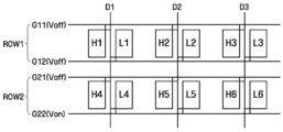
도 3을 참조하면, 하나의 화소(PX)열이 활성화되어 데이터 전압을 입력받는 시간을 1 수평 주기(이하 "1H"라 함)라고 하면, 1 H동안 각 화소열의 제1 및 제2 게이트 라인이 순차적으로 활성화된다. 즉, 첫 1H에서 제1 구간(P1) 동안 제1 화소열(ROW1)의 제1 게이트 라인(G11)이 활성화되고, 제2 구간(P2) 동안 제1 화소열(ROW1)의 제2 게이트 라인(G12)이 활성화된다. 두번째 1H에서 제3 구간(P3) 동안 제2 화소열(ROW2)의 제1 게이트 라인(G21)이 활성화되고, 제2 구간(P2) 동안 제2 화소열(ROW2)의 제2 게이트 라인(G22)이 활성화된다.Referring to FIG. 3, when one pixel PX column is activated to receive a data voltage as one horizontal period (hereinafter, referred to as “1H”), the first and second gate lines of each pixel column for 1 H may be referred to. This is activated sequentially. That is, in the first 1H, the first gate line G11 of the first pixel column ROW1 is activated during the first period P1, and the second gate line of the first pixel column ROW1 during the second period P2. (G12) is activated. In the second 1H, the first gate line G21 of the second pixel column ROW2 is activated during the third period P3, and the second gate line G22 of the second pixel column ROW2 during the second period P2. ) Is activated.
한편 도 1의 데이터 드라이버(500)는 타이밍 컨트롤러(600)로부터 제공된 데이터 제어 신호(CONT2)에 응답하여 먼저 다수의 제1 서브 영상 신호(HDAT)에 대응하는 다수의 제1 서브 데이터 전압을 각 데이터 라인(D1-Dm)에 인가하고, 다음으로 다수의 제2 서브 영상 신호(LDAT)의 다수의 제2 서브 데이터 전압을 각 데이터 라인에 인가한다. 데이터 드라이버(500)는 계조 전압 생성부(800)으로부터 다수의 제1 서브 영상 신호(HDAT)에 대응하는 다수의 제1 서브 데이터 전압 및 다수의 제2 서브 영상 신호(LDAT)에 대응하는 다수의 제2 서브 데이터 전압을 입력받는다.Meanwhile, in response to the data control signal CONT2 provided from the
도 3, 도 4a 내지 도 4d를 더 참조하여 좀더 구체적으로 설명한다. It will be described in more detail with reference to Figures 3, 4a to 4d.
제1 구간(P1) 동안 제1 화소열(ROW1)의 제1 게이트 라인(G11)에 게이트 온 전압(Von)이 인가되고, 나머지 게이트 라인(G12, G21, G22)에 게이트 오프 전압(Voff)이 인가된다. 데이터 드라이버(500)가 먼저 다수의 제1 서브 데이터 전 압(H1, H2, H3)을 각 데이터 라인(D1, D2, D3)에 인가한다. 따라서 도 4a에 도시된 바와 같이 제1 화소열(ROW1)의 다수의 제1 서브 화소(SP1)에 각 제1 서브 데이터 전압(H1, H2, H3)이 제공된다.The gate-on voltage Von is applied to the first gate line G11 of the first pixel column ROW1 during the first period P1, and the gate-off voltage Voff is applied to the remaining gate lines G12, G21, and G22. Is applied. The
제2 구간(P2) 동안 제1 화소열(ROW1)의 제2 게이트 라인(G12)에 게이트 온 전압(Von)이 인가되고, 나머지 게이트 라인(G11, G21, G22)에 게이트 오프 전압(Voff)이 인가된다. 데이터 드라이버(500)가 다수의 제2 서브 데이터 전압(L1, L2, L3)을 각 데이터 라인(D1, D2, D3)에 인가한다. 따라서 도 4b에 도시된 바와 같이 제1 화소열(ROW1)의 다수의 제2 서브 화소(SP2)에 각 제2 서브 데이터 전압(L1, L2, L3)이 제공된다.The gate-on voltage Von is applied to the second gate line G12 of the first pixel column ROW1 during the second period P2, and the gate-off voltage Voff is applied to the remaining gate lines G11, G21, and G22. Is applied. The
제3 구간(P3) 동안 제2 화소열(ROW2)의 제1 게이트 라인(G21)에 게이트 온 전압(Von)이 인가되고, 나머지 게이트 라인(G11, G12, G22)에 게이트 오프 전압(Voff)이 인가된다. 데이터 드라이버(500)가 다수의 제1 서브 데이터 전압(H4, H5, H6)을 각 데이터 라인(D1, D2, D3)에 인가한다. 따라서 도 4c에 도시된 바와 같이 제2 화소열(ROW2)의 다수의 제1 서브 화소(SP1)에 각 제1 서브 데이터 전압(H4, H5, H6)이 제공된다.The gate-on voltage Von is applied to the first gate line G21 of the second pixel column ROW2 during the third period P3, and the gate-off voltage Voff is applied to the remaining gate lines G11, G12, and G22. Is applied. The
제4 구간(P4) 동안 제2 화소열(ROW2)의 제2 게이트 라인(G22)에 게이트 온 전압(Von)이 인가되고, 나머지 게이트 라인(G11, G12, G21)에 게이트 오프 전압(Voff)이 인가된다. 데이터 드라이버(500)가 다수의 제2 서브 데이터 전압(L4, L5, L6)을 각 데이터 라인(D1, D2, D3)에 인가한다. 따라서 도 4d에 도시된 바와 같이 제2 화소열(ROW2)의 다수의 제2 서브 화소(SP2)에 각 제2 서브 데이터 전 압(L4, L5, L6)이 제공된다.The gate-on voltage Von is applied to the second gate line G22 of the second pixel column ROW2 during the fourth period P4, and the gate-off voltage Voff is applied to the remaining gate lines G11, G12, and G21. Is applied. The
도 5를 참조하여 룩업 테이블(700)에 저장된 제1 서브 영상 신호(HDAT) 및 제2 서브 영상 신호(LDAT)를 설명한다.A first sub image signal HDAT and a second sub image signal LDAT stored in the lookup table 700 will be described with reference to FIG. 5.
도 5를 참조하면, 액정 패널(300)로 인가되는 그레이에 따른 휘도 특성을 보여주는 감마 곡선을 나타낸다. 액정 표시 장치(10)의 제조 단계에서 상기 액정 패널(300)의 측면 시인성이 최적이 되는 상기 제1 서브 화소(SP1)의 감마 곡선(A)과 상기 제 2 서브 화소(PX)의 감마 곡선(B)을 설정한다. 상기 제 1 서브 화소(PX)의 감마 곡선(A)과 상기 제 2 서브 화소(PX)의 감마 곡선(B)은 상기 액정 표시 장치(10)의 특성 및 기능에 따라 차이가 날 수 있다.Referring to FIG. 5, a gamma curve showing luminance characteristics according to gray applied to the
액정 패널(300)의 제 1 서브 화소(PX)와 상기 제 2 서브 화소(PX)에 동일한 그레이 레벨에 해당하는 데이터 전압을 인가한 후, 액정 패널(300)의 정면에서의 휘도 특성을 감지하여 상기 액정 패널(300)의 정면에서의 감마 곡선(A+B)을 구한다. 액정 패널(300)의 정면에서의 감마 곡선(A+B)과 기 설정된 제 1 서브 화소(PX)의 감마 곡선(A)과 상기 제 2 서브 화소(PX)의 감마 곡선(B)을 이용하여 룩업 테이블(700)에 제1 서브 영상 신호(HDAT) 및 제2 서브 영상 신호(LDAT)를 저장한다.After applying a data voltage corresponding to the same gray level to the first sub-pixel PX and the second sub-pixel PX of the
예를 들어, 액정 패널(300)의 제1 서브 화소(SP1)와 제2 서브 화소(SP2)에 동일한 제1 그레이(130G)에 해당하는 서브 데이터 전압을 인가하면, 액정 패널(100)의 정면에서는 제1 휘도(L1) 값을 갖는다. 액정 패널(300)로 인가된 제1 그레이(130G)와 상기 액정 패널(100)로부터 감지된 제 1 휘도(L1) 값이 만나는 제1 접점(P1)을 휘도 축의 방향으로 직선으로 연장하여 제1 서브 화소(SP1)의 감마 곡 선(A)과 접하는 제2 접점(P2)과 상기 제 2 서브 화소(SP2)의 감마 곡선(B)과 접하는 제3 접점(P3)을 구한다. 제1 서브 화소(SP1)의 감마 곡선(A) 상에서 제2 접점(P2)은 제2 휘도(L2) 값을 갖는다. 액정 패널(300)의 정면 감마 곡선(A+B) 상에서 제2 휘도(L2)에 해당하는 계조 값은 제2 그레이(220G)가 된다. 마찬가지로, 제2 서브 화소(SP2)의 감마 곡선(B) 상에서 제3 접점(P3)은 제3 휘도(L3) 값을 갖는다. 액정 패널(300)의 정면 감마 곡선(A+B) 상에서 제3 휘도(L3)에 해당하는 그레이 값은 제3 그레이(35G)가 된다.For example, when a sub data voltage corresponding to the same first gray 130G is applied to the first sub pixel SP1 and the second sub pixel SP2 of the
즉, 액정 패널(300)의 정면에서 감마 특성이 제1 접점(P1)으로 표현되기 위해서는, 제1 서브 화소(SP1)에는 제2 그레이(220G)에 해당하는 서브 데이터 전압이 인가되어야 하고, 제2 서브 화소(SP2)에는 제3 그레이(35G)에 해당하는 서브 데이터 전압이 인가되어야 한다.That is, in order for the gamma characteristic to be expressed as the first contact point P1 in front of the
상술한 방법으로, 외부로부터 입력되는 영상 신호(ISIG)의 각 그레이에 대응하여 제1 및 제2 서브 화소(SP1, SP2)에 인가할 제1 서브 데이터 전압 및 제2 서브 데이터 전압에 대응하는 제1 서브 영상 신호(HDAT) 및 제2 서브 영상 신호(LDAT)를 룩업 테이블(700)에 저장할 수 있다. In the above-described method, a first sub data voltage and a second sub data voltage to be applied to the first and second sub pixels SP1 and SP2 corresponding to the respective grays of the image signal ISIG input from the outside. The first sub image signal HDAT and the second sub image signal LDAT may be stored in the lookup table 700.
상술한 바와 같이, 영상 신호(ISIG)를 측면 시인성을 최적화할 수 있는 제1 및 제2 서브 영상 신호(LDAT)로 변환하여 각 제1 및 제2 서브 화소(SP1, SP2)에 제1 및 제2 서브 데이터 전압을 제공하므로 표시 품질이 향상된다.As described above, the first and second sub pixels SP1 and SP2 are converted into first and second sub image signals LDAT by converting the image signal ISIG into first and second sub image signals LDAT capable of optimizing side visibility. Providing 2 sub data voltages improves display quality.
한편, 제1 및 제2 서브 화소(SP1, SP2)는 하나의 데이터 라인을 공유하므로, 표시 구동부는 다수의 제1 서브 데이터 전압을 먼저 각 데이터 라인(D1-Dm)에 인가 하고, 다음으로 다수의 제2 서브 데이터 전압을 각 데이터 라인(D1-Dm)에 인가하여야 한다. On the other hand, since the first and second sub-pixels SP1 and SP2 share one data line, the display driver first applies a plurality of first sub-data voltages to each of the data lines D1-Dm, and then, The second sub data voltage of must be applied to each data line D1 -Dm.
이를 위해 첫번째 방법은 타이밍 컨트롤러(600)가 먼저 다수의 제1 서브 영상 신호(HDAT)를 제공하고, 다음으로 다수의 제2 서브 영상 신호(LDAT)를 제공할 수 있다. 이때 데이터 드라이버(500)는 타이밍 컨트롤러(600)로부터 순차적으로 출력되는 다수의 제1 서브 영상 신호(HDAT)를 먼저 다수의 제1 서브 데이터 전압으로 변환하여 출력하고, 다음으로 다수의 제2 서브 영상 신호(LDAT)를 제2 서브 데이터 전압으로 변환하여 출력하는 것이다. To this end, in the first method, the
두번째 방법은 타이밍 컨트롤러(600)가 입력되는 영상 신호(ISIG)에 대응하는 제1 서브 영상 신호(HDAT)와 제2 서브 영상 신호(LDAT)를 출력하고, 데이터 드라이버(500)가 출력된 다수의 제1 및 제2 서브 영상 신호(HDAT, LDAT) 중에서 먼저 다수의 제1 서브 영상 신호(HDAT)를 다수의 제1 서브 데이터 전압으로 변환하여 출력하고, 다음으로 다수의 제2 서브 영상 신호(LDAT)를 다수의 제2 서브 데이터 전압으로 변환하여 출력할 수 있다. In a second method, the
본 발명에 따른 표시 장치는 상기 두 가지 방법에 한정되지 않고, 다양한 방법으로 동작될 수 있다. 이하에서는 상술한 첫번째 방법으로 동작하는 표시 장치를 구체적인 실시예들을 통해 설명한다.The display device according to the present invention is not limited to the above two methods and can be operated in various ways. Hereinafter, a display device operating in the first method described above will be described with reference to specific embodiments.
도 6 및 도 7을 참조하여 본 발명의 일 실시예에 따른 표시 장치를 설명한다. 도 6은 본 발명의 일 실시예에 따른 표시 장치 및 그의 구동 방법을 설명하기 위한 표시 장치의 타이밍 컨트롤러를 설명하기 위한 블록도이고, 도 7은 도 6의 타 이밍 컨트롤러의 동작을 설명하기 위한 개념도이다.A display device according to an exemplary embodiment of the present invention will be described with reference to FIGS. 6 and 7. FIG. 6 is a block diagram illustrating a timing controller of a display device for explaining a display device and a driving method thereof according to an embodiment of the present invention, and FIG. 7 is a conceptual diagram for describing an operation of the timing controller of FIG. 6. to be.
도 6을 참조하면, 타이밍 컨트롤러(601)는 메모리 컨트롤러(610)와, 저장부(620)와 출력부(630)를 포함한다.Referring to FIG. 6, the
먼저 메모리 컨트롤러(610)는 영상 신호(ISIG)를 입력받아 이에 대응하는 제1 서브 영상 신호(HDAT) 및 제2 서브 영상 신호(LDAT)를 룩업 테이블(700)로부터 독출한다. 여기서 메모리 컨트롤러(610)는 제1 서브 영상 신호(HDAT) 및 제2 서브 영상 신호(LDAT)를 동시에 독출할 수 있고, 또는 순차적으로 독출할 수 있다.First, the
저장부(620)는 메모리 컨트롤러(610)로부터 출력된 제1 서브 영상 신호(HDAT) 및 제2 서브 영상 신호(LDAT)를 저장한다. 저장부(620)는 한 화소열의 다수의 제1 서브 화소(SP1)에 제공될 다수의 제1 서브 영상 신호(HDAT)를 다수의 제2 서브 영상 신호(LDAT)보다 먼저 출력하기 위해 다수의 제1 서브 영상 신호(HDAT) 및 제2 서브 영상 신호(LDAT)를 저장한다. 출력부(630)는 메모리에 저장되어 있는 다수의 제1 서브 영상 신호(HDAT)를 먼저 출력하고, 다음으로 다수의 제2 서브 영상 신호(LDAT)를 출력한다.The
여기서 도 7을 더 참조하여 저장부(620)와 출력부(630)의 동작을 좀더 상세히 설명한다. 이하에서 한 화소열에 4개의 화소(PX)를 포함하는 경우를 예로 들어 설명한다. 한 화소(PX)열은 4개의 제1 서브 화소(SP1)와 4개의 제2 서브 화소(SP2)를 포함한다. Herein, the operations of the
먼저 시간 T1에서 저장부(620)는 제1 화소열의 3개의 제1 서브 화소(SP1)에 제공될 3개의 제1 서브 영상 신호(HDAT1_1, HDAT1_2, HDAT1_3)와 3개의 제2 서브 화소(SP2)에 제공될 3개의 제2 서브 영상 신호(LDAT1_1, LDAT1_2, LDAT1_3)를 저장한다.First, at time T1, the
다음으로 메모리 컨트롤러(610)가 제1 화소열의 네번째 화소(PX)에 제공될 제1 서브 영상 신호(HDAT1_4) 및 제2 서브 영상 신호(LDAT1_4)를 제공하면, 시간 T2에서 저장부(620)는 제1 서브 영상 신호(HDAT1_4) 및 제2 서브 영상 신호(LDAT1_4)를 저장한다. 이때 출력부(630)는 메모리로부터 첫번째 화소(PX) 및 두번째 화소(PX)에 제공될 제1 서브 영상 신호(HDAT1_1, HDAT1_2)를 출력한다.Next, when the
다음으로 메모리 컨트롤러(610)가 제2 화소열의 첫번째 화소(PX)에 제공될 제1 서브 영상 신호(HDAT2_1) 및 제2 서브 영상 신호(LDAT2_1)를 제공하면, 시간 T3에서 저장부(620)는 제1 서브 영상 신호(HDAT2_1) 및 제2 서브 영상 신호(LDAT2_1)를 저장한다. 이때 출력부(630)는 저장부(620)로부터 세번째 화소(PX) 및 네번째 화소(PX)에 제공될 제1 서브 영상 신호(HDAT1_3, HDAT1_4)를 출력한다.Next, when the
다음으로 메모리 컨트롤러(610)가 제2 화소열의 두번째 화소(PX)에 제공될 제1 서브 영상 신호(HDAT2_2) 및 제2 서브 영상 신호(LDAT2_2)를 제공하면, 시간 T4에서 저장부(620)는 제1 서브 영상 신호(HDAT)(HDAT2_2) 및 제2 서브 영상 신호(LDAT2_2)를 저장한다. 이때 출력부(630)는 저장부(620)로부터 제1 화소열의 첫번째 화소(PX) 및 두번째 화소(PX)에 제공될 제2 서브 영상 신호(LDAT1_2, LDAT1_1)를 출력한다.Next, when the
다음으로 메모리 컨트롤러(610)가 제2 화소열의 세번째 화소(PX)에 제공될 제1 서브 영상 신호(HDAT2_3) 및 제2 서브 영상 신호(LDAT2_3)를 제공하면, 시간 T5에서 저장부(620)는 제1 서브 영상 신호(HDAT2_3) 및 제2 서브 영상 신호(LDAT2_3)를 저장한다. 이때 출력부(630)는 저장부(620)로부터 제1 화소(PX)열의 세번째 화소(PX) 및 네번째 화소(PX)에 제공될 제2 서브 영상 신호(LDAT1_3, LDAT1_4)를 출력한다.Next, when the
정리해서 설명하면, 저장부(620)는 메모리 컨트롤러(610)로부터 출력된 제1 서브 영상 신호(HDAT) 및 제2 서브 영상 신호(LDAT)를 저장하고, 출력부(630)가 저장부(620)로부터 한 화소(PX)열에 대한 다수의 제1 서브 영상 신호(HDAT)를 먼저 출력하고, 다음으로 한 화소(PX)열에 대한 다수의 제2 서브 영상 신호(LDAT)를 출력한다.In summary, the
도 8 및 도 9를 참조하여, 본 발명의 다른 실시예에 따른 표시 장치 및 그의 구동 방법을 설명한다. 도 8은 본 발명의 다른 실시예에 따른 표시 장치 및 그의 구동 방법을 설명하기 위한 표시 장치의 타이밍 컨트롤러의 블록도이고, 도 9는 도 8의 타이밍 컨트로러의 동작을 설명하기 위한 개념도이다. 도 6에 도시된 구성 요소와 동일한 기능을 하는 구성 요소에 대해서는 동일한 도면 부호를 사용하고, 설명의 편의상 해당 구성 요소의 상세한 설명은 생략한다.8 and 9, a display device and a driving method thereof according to another exemplary embodiment will be described. 8 is a block diagram of a timing controller of a display device for explaining a display device and a driving method thereof according to another embodiment of the present invention, and FIG. 9 is a conceptual diagram for describing an operation of the timing controller of FIG. 8. The same reference numerals are used for components that have the same function as the components shown in FIG. 6, and detailed descriptions of the corresponding components are omitted for convenience of description.
도 8을 참조하면 타이밍 컨트롤러(602)는 저장부(640)와 메모리 컨트롤러(650)를 포함한다.Referring to FIG. 8, the
저장부(640)는 영상 신호(ISIG)를 입력받아 저장한다. 메모리 컨트롤러(650)는 저장부(640)에 저장된 영상 신호(ISIG)를 입력받아 이에 대응하는 다수의 제1 서브 영상 신호(HDAT)를 먼저 독출하여 출력하고, 다음으로 다수의 제2 서브 영상 신호(LDAT)를 독출하여 출력한다.The
도 9를 더 참조하여 저장부(640)와 메모리 컨트롤러(650)의 동작을 좀더 상세히 설명한다. 이하에서 한 화소열에 4개의 화소(PX)를 포함하는 경우를 예로 들어 설명한다. 한 화소열은 4개의 제1 서브 화소(SP1)와 4개의 제2 서브 화소(SP2)를 포함한다. Referring to FIG. 9, operations of the
먼저 시간 T1에서 저장부(640)는 제1 화소열의 3개의 화소(PX)에 제공될 3개의 영상 신호(ISIG1_1, ISIG1_2, ISIG1_3)를 저장한다.First, at a time T1, the
시간 T2에서 저장부(640)가 제1 화소열의 네번째 화소(PX)에 제공될 영상 신호(ISIG1_4)를 저장한다. 이때, 메모리 컨트롤러(650)는 먼저 제1 화소열의 첫번째 화소(PX)에 제공될 영상 신호(ISIG1_1)를 입력받아 이에 대응하는 제1 서브 영상 신호(HDAT1_1)를 룩업 테이블(700)로부터 독출하여 출력한다. 다음으로, 제1 화소열의 두번째 화소(PX)에 제공될 영상 신호(ISIG1_2)를 입력받아 이에 대응하는 제1 서브 영상 신호(HDAT1_2)를 룩업 테이블(700)로부터 독출하여 출력한다At a time T2, the
시간 T3에서 저장부(640)가 제2 화소(PX)열의 첫번째 화소(PX)에 제공될 영상 신호(ISIG2_1)를 저장한다. 이때, 메모리 컨트롤러(650)는 먼저 제1 화소열의 세번째 화소(PX)에 제공될 영상 신호(ISIG1_3)를 입력받아 이에 대응하는 제1 서브 영상 신호(HDAT1_3)를 룩업 테이블(700)로부터 독출하여 출력한다. 다음으로, 제1 화소열의 네번째 화소(PX)에 제공될 영상 신호(ISIG1_4)를 입력받아 이에 대응하는 제1 서브 영상 신호(HDAT1_4)를 룩업 테이블(700)로부터 독출하여 출력한다At time T3, the
시간 T4에서 저장부(640)가 제2 화소열의 두번째 화소(PX)에 제공될 영상 신 호(ISIG2_2)를 저장한다. 이때, 메모리 컨트롤러(650)는 먼저 제1 화소열의 첫번째 화소(PX)에 제공될 영상 신호(ISIG1_1)를 입력받아 이에 대응하는 제2 서브 영상 신호(LDAT1_1)를 룩업 테이블(700)로부터 독출하여 출력한다. 다음으로, 제1 화소(PX)열의 두번째 화소(PX)에 제공될 영상 신호(ISIG1_2)를 입력받아 이에 대응하는 제2 서브 영상 신호(LDAT1_4)를 룩업 테이블(700)로부터 독출하여 출력한다At time T4, the
시간 T5에서 저장부(640)가 제2 화소(PX)열의 세번째 화소(PX)에 제공될 영상 신호(ISIG2_3)를 저장한다. 이때, 메모리 컨트롤러(650)는 먼저 제1 화소열의 세번째 화소(PX)에 제공된 영상 신호(ISIG1_3)를 입력받아 이에 대응하는 제2 서브 영상 신호(LDAT1_3)를 룩업 테이블(700)로부터 독출하여 출력한다. 다음으로, 제1 화소(PX)열의 네번째 화소(PX)에 제공될 영상 신호(ISIG1_4)를 입력받아 이에 대응하는 제2 서브 영상 신호(LDAT1_4)를 룩업 테이블(700)로부터 독출하여 출력한다At a time T5, the
정리해서 설명하면, 저장부(640)는 영상 신호(ISIG)를 저장하고, 메모리 컨트롤러(650)가 한 화소열에 대한 영상 신호(ISIG)에 대응하는 다수의 제1 서브 영상 신호(HDAT)를 먼저 독출하여 출력하고, 다음으로 한 화소열에 대한 다수의 제2 서브 영상 신호(LDAT)를 독출하여 출력한다.In summary, the
이상 첨부된 도면을 참조하여 본 발명의 실시예들을 설명하였지만, 본 발명이 속하는 기술분야에서 통상의 지식을 가진 자는 본 발명이 그 기술적 사상이나 필수적인 특징을 변경하지 않고서 다른 구체적인 형태로 실시될 수 있다는 것을 이해할 수 있을 것이다. 그러므로 이상에서 기술한 실시예들은 모든 면에서 예시적인 것이며 한정적이 아닌 것으로 이해해야만 한다.Although embodiments of the present invention have been described above with reference to the accompanying drawings, those skilled in the art to which the present invention pertains may implement the present invention in other specific forms without changing the technical spirit or essential features thereof. I can understand that. Therefore, it should be understood that the embodiments described above are exemplary in all respects and not restrictive.
도 1은 본 발명의 실시예들에 따른 표시 장치 및 그의 구동 방법을 설명하기 위한 블록도이다.1 is a block diagram illustrating a display device and a driving method thereof according to embodiments of the present invention.
도 2는 도 1의 한 화소의 등가회로도이다.FIG. 2 is an equivalent circuit diagram of one pixel of FIG. 1.
도 3 내지 도 4d는 표시 구동부의 동작을 설명하기 위한 신호도 및 개념도이다.3 to 4D are signal diagrams and conceptual diagrams for describing an operation of the display driver.
도 5는 도 1의 룩업 테이블에 저장된 제1 서브 영상 신호 및 제2 서브 영상 신호를 설명하기 위한 그래프이다.FIG. 5 is a graph for describing a first sub image signal and a second sub image signal stored in the lookup table of FIG. 1.
도 6은 본 발명의 일 실시예에 따른 표시 장치 및 그의 구동 방법을 설명하기 위한 표시 장치의 타이밍 컨트롤러를 설명하기 위한 블록도이다.6 is a block diagram illustrating a timing controller of a display device for explaining a display device and a driving method thereof according to an exemplary embodiment of the present invention.
도 7은 도 6의 타이밍 컨트롤러의 동작을 설명하기 위한 개념도이다.FIG. 7 is a conceptual diagram for describing an operation of the timing controller of FIG. 6.
도 8은 본 발명의 다른 실시예에 따른 표시 장치 및 그의 구동 방법을 설명하기 위한 표시 장치의 타이밍 컨트롤러의 블록도이다.8 is a block diagram of a timing controller of a display device for explaining a display device and a driving method thereof according to another embodiment of the present invention.
도 9는 도 8의 타이밍 컨트로러의 동작을 설명하기 위한 개념도이다.FIG. 9 is a conceptual diagram for describing an operation of the timing controller of FIG. 8.
(도면의 주요부분에 대한 부호의 설명)(Explanation of symbols for the main parts of the drawing)
10: 액정 표시 장치 100: 제1 기판10: liquid crystal display device 100: first substrate
200: 제2 기판 300: 액정 패널200: second substrate 300: liquid crystal panel
400: 게이트 드라이버 500: 데이터 드라이버400: gate driver 500: data driver
600: 타이밍 컨트롤러 610: 메모리 컨트롤러600: timing controller 610: memory controller
620: 저장부 643: 출력부620: storage unit 643: output unit
700: 룩업 테이블 800: 계조 전압 생성부700: lookup table 800: gray voltage generator
Claims (19)
Priority Applications (6)
| Application Number | Priority Date | Filing Date | Title |
|---|---|---|---|
| KR1020080005080A KR20090079108A (en) | 2008-01-16 | 2008-01-16 | Display device and driving method of the same |
| US12/261,507 US8144163B2 (en) | 2008-01-16 | 2008-10-30 | Driving device and driving method of the same |
| JP2008293344A JP2009169398A (en) | 2008-01-16 | 2008-11-17 | Display device and method of driving the same |
| EP08022588A EP2081181A3 (en) | 2008-01-16 | 2008-12-31 | Driving device and driving method of the same |
| TW098100049A TWI451375B (en) | 2008-01-16 | 2009-01-05 | Driving device and driving method of the same |
| CNA2009100001145A CN101488311A (en) | 2008-01-16 | 2009-01-06 | Driving device and driving method of the same |
Applications Claiming Priority (1)
| Application Number | Priority Date | Filing Date | Title |
|---|---|---|---|
| KR1020080005080A KR20090079108A (en) | 2008-01-16 | 2008-01-16 | Display device and driving method of the same |
Publications (1)
| Publication Number | Publication Date |
|---|---|
| KR20090079108A true KR20090079108A (en) | 2009-07-21 |
Family
ID=40451199
Family Applications (1)
| Application Number | Title | Priority Date | Filing Date |
|---|---|---|---|
| KR1020080005080A KR20090079108A (en) | 2008-01-16 | 2008-01-16 | Display device and driving method of the same |
Country Status (6)
| Country | Link |
|---|---|
| US (1) | US8144163B2 (en) |
| EP (1) | EP2081181A3 (en) |
| JP (1) | JP2009169398A (en) |
| KR (1) | KR20090079108A (en) |
| CN (1) | CN101488311A (en) |
| TW (1) | TWI451375B (en) |
Cited By (2)
| Publication number | Priority date | Publication date | Assignee | Title |
|---|---|---|---|---|
| KR20140013311A (en) * | 2012-07-23 | 2014-02-05 | 삼성디스플레이 주식회사 | Display device and driving method thereof |
| US9368055B2 (en) | 2013-08-19 | 2016-06-14 | Samsung Display Co., Ltd. | Display device and driving method thereof for improving side visibility |
Families Citing this family (9)
| Publication number | Priority date | Publication date | Assignee | Title |
|---|---|---|---|---|
| KR101783975B1 (en) * | 2010-07-14 | 2017-10-11 | 삼성디스플레이 주식회사 | Three dimensional image display device |
| WO2012063696A1 (en) * | 2010-11-10 | 2012-05-18 | シャープ株式会社 | Liquid-crystal display device |
| TWI411992B (en) * | 2010-12-14 | 2013-10-11 | Au Optronics Corp | Driving method of display apparatus and display apparatus |
| KR102024159B1 (en) | 2013-02-05 | 2019-09-24 | 삼성디스플레이 주식회사 | Liquid crystal display |
| CN103293809B (en) * | 2013-05-28 | 2015-09-30 | 深圳市华星光电技术有限公司 | Anti-colour cast display panel |
| KR102128970B1 (en) | 2013-12-18 | 2020-07-02 | 삼성디스플레이 주식회사 | Liquid crystal display |
| TW201533726A (en) * | 2014-02-17 | 2015-09-01 | Au Optronics Corp | Image display method of half-source-driving liquid crystal display |
| CN104992688B (en) | 2015-08-05 | 2018-01-09 | 京东方科技集团股份有限公司 | Pel array, display device and its driving method and drive device |
| CN105204256B (en) * | 2015-10-29 | 2018-10-19 | 深圳市华星光电技术有限公司 | A kind of array substrate and its display device based on data line common technology |
Citations (2)
| Publication number | Priority date | Publication date | Assignee | Title |
|---|---|---|---|---|
| KR20070034145A (en) * | 2005-09-23 | 2007-03-28 | 삼성전자주식회사 | Liquid crystal display panel, its driving method and liquid crystal display device using same |
| KR20070063173A (en) * | 2005-12-14 | 2007-06-19 | 삼성전자주식회사 | Liquid crystal display, method of modifying image signals and driving method thereof |
Family Cites Families (14)
| Publication number | Priority date | Publication date | Assignee | Title |
|---|---|---|---|---|
| US6040812A (en) * | 1996-06-19 | 2000-03-21 | Xerox Corporation | Active matrix display with integrated drive circuitry |
| KR100890025B1 (en) * | 2002-12-04 | 2009-03-25 | 삼성전자주식회사 | Liquid crystal display and apparatus and method of driving liquid crystal display |
| US8810606B2 (en) * | 2004-11-12 | 2014-08-19 | Samsung Display Co., Ltd. | Display device and driving method thereof |
| KR20060111148A (en) * | 2005-04-22 | 2006-10-26 | 삼성전자주식회사 | Driving apparatus of display device and driving method thereof |
| KR20060116443A (en) * | 2005-05-10 | 2006-11-15 | 삼성전자주식회사 | Display device, apparatus and method for driving thereof |
| JP4824387B2 (en) * | 2005-10-28 | 2011-11-30 | ルネサスエレクトロニクス株式会社 | LCD driver circuit |
| KR101246756B1 (en) * | 2006-02-03 | 2013-03-26 | 삼성디스플레이 주식회사 | Liquid crystal display and method of manufacturing the same |
| KR101256011B1 (en) * | 2006-04-17 | 2013-04-18 | 삼성디스플레이 주식회사 | Driving device and display apparatus having the same |
| KR101226217B1 (en) | 2006-06-15 | 2013-02-07 | 삼성디스플레이 주식회사 | Signal processing device and liquid crystal display comprising the same |
| JP5376774B2 (en) * | 2006-07-21 | 2013-12-25 | 三星ディスプレイ株式會社 | Liquid crystal display |
| CN100516998C (en) * | 2006-11-17 | 2009-07-22 | 群康科技(深圳)有限公司 | Liquid crystal display device and its driving method |
| KR20080056493A (en) * | 2006-12-18 | 2008-06-23 | 삼성전자주식회사 | Thin film transistor substrate and method of manufacturing the same |
| KR101335424B1 (en) * | 2006-12-29 | 2013-12-02 | 엘지디스플레이 주식회사 | driving method of a built in image sensor for liquid crystal display device |
| JP5312779B2 (en) * | 2007-12-13 | 2013-10-09 | ルネサスエレクトロニクス株式会社 | Liquid crystal display device, data driving IC, and liquid crystal display panel driving method |
-
2008
- 2008-01-16 KR KR1020080005080A patent/KR20090079108A/en not_active Application Discontinuation
- 2008-10-30 US US12/261,507 patent/US8144163B2/en not_active Expired - Fee Related
- 2008-11-17 JP JP2008293344A patent/JP2009169398A/en active Pending
- 2008-12-31 EP EP08022588A patent/EP2081181A3/en not_active Ceased
-
2009
- 2009-01-05 TW TW098100049A patent/TWI451375B/en not_active IP Right Cessation
- 2009-01-06 CN CNA2009100001145A patent/CN101488311A/en active Pending
Patent Citations (2)
| Publication number | Priority date | Publication date | Assignee | Title |
|---|---|---|---|---|
| KR20070034145A (en) * | 2005-09-23 | 2007-03-28 | 삼성전자주식회사 | Liquid crystal display panel, its driving method and liquid crystal display device using same |
| KR20070063173A (en) * | 2005-12-14 | 2007-06-19 | 삼성전자주식회사 | Liquid crystal display, method of modifying image signals and driving method thereof |
Cited By (2)
| Publication number | Priority date | Publication date | Assignee | Title |
|---|---|---|---|---|
| KR20140013311A (en) * | 2012-07-23 | 2014-02-05 | 삼성디스플레이 주식회사 | Display device and driving method thereof |
| US9368055B2 (en) | 2013-08-19 | 2016-06-14 | Samsung Display Co., Ltd. | Display device and driving method thereof for improving side visibility |
Also Published As
| Publication number | Publication date |
|---|---|
| TWI451375B (en) | 2014-09-01 |
| JP2009169398A (en) | 2009-07-30 |
| EP2081181A2 (en) | 2009-07-22 |
| EP2081181A3 (en) | 2010-12-15 |
| TW200947383A (en) | 2009-11-16 |
| US8144163B2 (en) | 2012-03-27 |
| CN101488311A (en) | 2009-07-22 |
| US20090179906A1 (en) | 2009-07-16 |
Similar Documents
| Publication | Publication Date | Title |
|---|---|---|
| KR20090079108A (en) | Display device and driving method of the same | |
| KR101112554B1 (en) | Driving apparatus for display device and display device including the same | |
| CN101059945B (en) | Liquid crystal display driving device | |
| CN101059944B (en) | Driving device | |
| US7973751B2 (en) | Display device using adapted double gamma curves | |
| US7898536B2 (en) | Display apparatus and method of driving the same | |
| US20070195041A1 (en) | Liquid crystal display device having improved side visibility | |
| KR101513150B1 (en) | Display apparatus and timing controller therein | |
| TW201715498A (en) | Display panel | |
| KR20080109512A (en) | Display apparatus and method of driving the same | |
| KR20060090419A (en) | Gate driving method and gate driver and display device having the same | |
| KR20100056228A (en) | Liquid crystal display and driving method of the same | |
| KR20090107578A (en) | Method of generating data for driving a display panel, data driving circuit for performing the methode and display apparatus having the data driving circuit | |
| KR20130065380A (en) | Liquid crystal display and driving method of the same | |
| KR20070048514A (en) | Liquid crystal display and method for driving there of | |
| KR101230306B1 (en) | Driving apparatus for display device and display device including the same | |
| JP5069932B2 (en) | Signal processing device and liquid crystal display device having the same | |
| US8884860B2 (en) | Liquid crystal display having increased response speed, and device and method for modifying image signal to provide increased response speed | |
| KR20080017626A (en) | Liquid display device | |
| US9292942B2 (en) | Image signal compensation apparatus and liquid crystal display including the same | |
| US20080062210A1 (en) | Driving device, display apparatus having the same and method of driving the display apparatus | |
| KR20080046981A (en) | Liquid crystal display and method of modifying image signals for liquid crystal display | |
| KR20070018721A (en) | Liquid crystal display device, method for controlling display data for liquid crystal display device, and recording media | |
| JP2007072450A (en) | Liquid crystal display, method for controlling display data of liquid crystal display and recording medium | |
| JP2014059506A (en) | Display device and method for rewriting look-up table |
Legal Events
| Date | Code | Title | Description |
|---|---|---|---|
| N231 | Notification of change of applicant | ||
| A201 | Request for examination | ||
| E902 | Notification of reason for refusal | ||
| E902 | Notification of reason for refusal | ||
| E90F | Notification of reason for final refusal | ||
| E601 | Decision to refuse application |