JP2009165285A - Semiconductor device - Google Patents
Semiconductor device Download PDFInfo
- Publication number
- JP2009165285A JP2009165285A JP2008001219A JP2008001219A JP2009165285A JP 2009165285 A JP2009165285 A JP 2009165285A JP 2008001219 A JP2008001219 A JP 2008001219A JP 2008001219 A JP2008001219 A JP 2008001219A JP 2009165285 A JP2009165285 A JP 2009165285A
- Authority
- JP
- Japan
- Prior art keywords
- current
- semiconductor element
- power semiconductor
- detection
- circuit
- Prior art date
- Legal status (The legal status is an assumption and is not a legal conclusion. Google has not performed a legal analysis and makes no representation as to the accuracy of the status listed.)
- Pending
Links
Images


Classifications
-
- H—ELECTRICITY
- H01—ELECTRIC ELEMENTS
- H01L—SEMICONDUCTOR DEVICES NOT COVERED BY CLASS H10
- H01L2924/00—Indexing scheme for arrangements or methods for connecting or disconnecting semiconductor or solid-state bodies as covered by H01L24/00
- H01L2924/0001—Technical content checked by a classifier
- H01L2924/0002—Not covered by any one of groups H01L24/00, H01L24/00 and H01L2224/00
Abstract
Description
本発明は、パワー半導体素子を有する半導体装置に関し、特に過熱保護機能と過電流保護機能を有する半導体装置に関するものである。 The present invention relates to a semiconductor device having a power semiconductor element, and more particularly to a semiconductor device having an overheat protection function and an overcurrent protection function.
半導体装置は、MOSFETやIGBT(Insulated Gate Bipolar Transistor)などのパワー半導体素子のメインデバイスと、これらを駆動制御するために各種の補助デバイスを集積した制御回路を組み合わせて、高性能化・多機能化が進められている。特に、信頼性を向上させるために過電流保護機能と過熱保護機能を搭載することが望ましいとされている。 Semiconductor devices are made high-performance and multifunctional by combining main devices of power semiconductor elements such as MOSFETs and IGBTs (Insulated Gate Bipolar Transistors) with control circuits that integrate various auxiliary devices to drive and control them. Is underway. In particular, it is desirable to mount an overcurrent protection function and an overheat protection function in order to improve reliability.
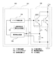
図9は過電流保護機能と過熱保護機能を兼ね備えた従来の半導体装置の構成例を示すブロック図である。 FIG. 9 is a block diagram showing a configuration example of a conventional semiconductor device having both an overcurrent protection function and an overheat protection function.
図9に示すように、半導体装置501は、メインデバイスチップ502と制御回路チップ503から構成される。メインデバイスチップ502は、主電流側と検出電流側でユニットセル数の比がM:1となるように並列接続された主電流側セルQMと電流検出側セルQSとで構成されたIGBTと、電流検出側セルQSに接続されたセンス抵抗RSと、主電流側セルQMの近隣に形成されたダイオードD1とで構成される。
As shown in FIG. 9, the
制御回路チップ503は、IGBT(QMおよびQS)のゲート端子へ送る駆動信号を制御するドライブ制御回路504と、センス抵抗RSに生じるセンス電圧VSの値に応じてIGBTの過電流を検出する過電流検出回路511と、ダイオードD1に定電流を流してダイオードD1の順方向電圧Vfの値に応じてIGBTの過熱を検出する過熱検出回路512とで構成される。
The
このようにすることで、メインデバイスであるIGBTを駆動するドライブ制御回路504は、IGBTの過電流または過熱を検出すると、IGBTのスイッチングを遮断することで、半導体装置501を保護することができる。なお、過熱検出に関しては、IGBTの過熱を検出するためのダイオードD1をメインデバイスチップ502内に配置することで、検出感度を高めている。
Thus, when the
また、特許文献1に開示されるように、過熱を検出するために電流検出用セルを利用することもある。この場合は、メインデバイスと同じチップ内に内蔵された2組の電流検出用セルのオン抵抗の温度依存性を利用して、それぞれの電流検出側セルに接続されたセンス抵抗に生じるセンス電圧の比より、過熱が検出される。
しかしながら、従来の複数の保護機能を兼ね備えた半導体装置では、制御回路チップとメインデバイスチップとの間に、過電流や過熱の検出信号を受け渡すための接続が複数必要となる。接続数の増加は、例えば、チップ−チップ間ワイヤーの増加であり、各チップ内にワイヤーボンディングパッドの増加も伴う。すなわち、制御回路とメインデバイスをマルチチップで構成された半導体装置では、複数の保護機能の搭載により信頼性が向上する一方で、組立コストのアップや半導体チップの有効面積の減少を招くという問題があった。 However, in a conventional semiconductor device having a plurality of protection functions, a plurality of connections for passing overcurrent and overheat detection signals are required between the control circuit chip and the main device chip. The increase in the number of connections is, for example, an increase in chip-to-chip wires, and is accompanied by an increase in wire bonding pads in each chip. That is, in a semiconductor device in which a control circuit and a main device are configured by a multi-chip, the reliability is improved by mounting a plurality of protection functions, while the assembly cost is increased and the effective area of the semiconductor chip is decreased. there were.
本発明は、前記従来技術の問題を解決することに指向するものであり、過電流保護機能と過熱保護機能を兼ね備えた半導体装置において、メインデバイスの過電流と過熱を感度良く検出するとともに、制御回路チップとメインデバイスチップとの間の接続を削減した半導体装置を提供することを目的とする。 The present invention is directed to solving the problems of the prior art, and in a semiconductor device having both an overcurrent protection function and an overheat protection function, the overcurrent and overheat of the main device are detected with high sensitivity and control. An object of the present invention is to provide a semiconductor device in which the connection between a circuit chip and a main device chip is reduced.
前記の目的を達成するために、本発明に係る請求項1に記載した半導体装置は、パワー半導体素子と、パワー半導体素子と同一基板上に形成し、パワー半導体素子に流れる電流を検出するための電流検出抵抗と、パワー半導体素子の過熱を検出するための電流を電流検出抵抗に印加する過熱検出用電流生成回路と、電流検出抵抗に生ずる電圧に対応して過電流または過熱を検出する異常検出回路と、異常検出回路の出力信号を受けてパワー半導体素子を駆動制御するドライブ制御回路とを備えたことを特徴とする。
In order to achieve the above object, a semiconductor device according to
これにより、電流検出抵抗に生ずる電圧をモニターすることで過電流だけでなく過熱も検出することができるため、パワー半導体素子を形成したチップとドライブ制御回路を形成したチップとのワイヤー接続を削減することができる。よって、各チップのワイヤーボンディングパッドも削減することができるため、チップ面積を有効に使うことができる。また、温度センサとなる電流検出抵抗を、パワー半導体素子を形成したチップ内に配置するため、過熱検出感度も良い。 As a result, it is possible to detect not only overcurrent but also overheat by monitoring the voltage generated in the current detection resistor, thereby reducing the wire connection between the chip on which the power semiconductor element is formed and the chip on which the drive control circuit is formed. be able to. Therefore, since the wire bonding pads of each chip can be reduced, the chip area can be used effectively. Moreover, since the current detection resistor serving as the temperature sensor is arranged in the chip on which the power semiconductor element is formed, the overheat detection sensitivity is also good.
また、請求項2に記載した半導体装置は、パワー半導体素子と、パワー半導体素子に流れる電流を検出するための電流検出抵抗と、パワー半導体素子と同一基板上に形成し、電流検出抵抗に接続した温度検出抵抗と、パワー半導体素子の過熱を検出するための電流を温度検出抵抗と電流検出抵抗とに印加する過熱検出用電流生成回路と、電流検出抵抗と温度検出抵抗に生ずる電圧の和に対応してパワー半導体素子の過電流または過熱を検出する異常検出回路と、異常検出回路の出力信号を受けてパワー半導体素子を駆動制御するドライブ制御回路とを備えたことを特徴とする。 The semiconductor device according to claim 2 is formed on the same substrate as the power semiconductor element, a current detection resistor for detecting a current flowing through the power semiconductor element, and connected to the current detection resistor. Corresponds to the sum of the voltage generated at the current detection resistor and the temperature detection resistor, the current detection circuit for applying the current to the temperature detection resistor and the current detection resistor to detect the overheating of the power semiconductor element. And an abnormality detection circuit for detecting an overcurrent or overheating of the power semiconductor element, and a drive control circuit for driving and controlling the power semiconductor element in response to an output signal of the abnormality detection circuit.
これにより、過熱検出用電流が温度検出抵抗と電流検出抵抗に印加されるため、過熱検出用電流の値が小さくでき、過熱を検出するための回路消費電力を低減することができる。 Thereby, since the overheat detection current is applied to the temperature detection resistor and the current detection resistor, the value of the overheat detection current can be reduced, and the circuit power consumption for detecting overheat can be reduced.
また、請求項3に記載した半導体装置は、請求項2の半導体装置における温度検出抵抗が、電流検出抵抗と異なる温度依存性を持つことを特徴とする。
The semiconductor device described in
温度検出抵抗と異なる作製方法で、温度依存性の小さい電流検出抵抗を形成することにより、過電流の検出レベルの温度依存性を小さくできる。さらに、温度検出抵抗の抵抗値を電流検出抵抗に対して大きく設定することで、過熱検出レベルに関しては温度検出抵抗の温度特性が支配的になり、過熱検出感度を大きく悪化させることはない。 By forming a current detection resistor having a small temperature dependency by a manufacturing method different from that of the temperature detection resistor, the temperature dependency of the overcurrent detection level can be reduced. Furthermore, by setting the resistance value of the temperature detection resistor to be larger than that of the current detection resistor, the temperature characteristic of the temperature detection resistor becomes dominant with respect to the overheat detection level, and the overheat detection sensitivity is not greatly deteriorated.
また、請求項4に記載した半導体装置は、請求項1〜3の半導体装置におけるパワー半導体素子が導通している期間が、過熱検出用電流生成回路から印加される電流が遮断されてパワー半導体素子の過電流のみを検出することを特徴とする。 According to a fourth aspect of the present invention, in the semiconductor device according to the first to third aspects, the current applied from the overheat detection current generating circuit is cut off during the period in which the power semiconductor element in the semiconductor device of the first to third embodiments is conductive. It is characterized by detecting only the overcurrent.
このようにすることで、パワー半導体が導通している期間には、過熱検出用電流の影響を受けることなく過電流を検出することができる。特に、ピーク電流を制御するパワー半導体素子においては、過電流の検出精度が重要となるため、有効である。 By doing in this way, overcurrent can be detected without being affected by overheat detection current during a period in which the power semiconductor is conducting. In particular, the power semiconductor element that controls the peak current is effective because the overcurrent detection accuracy is important.
また、請求項5に記載した半導体装置は、請求項4の半導体装置における過熱検出用電流生成回路の電流印加期間が、パワー半導体素子が遮断している期間の一部分であることを特徴とする。 The semiconductor device according to claim 5 is characterized in that the current application period of the overheat detection current generating circuit in the semiconductor device of claim 4 is a part of a period during which the power semiconductor element is cut off.
このようにすることで、異常検出回路が過熱を検出するために必要な過熱検出用電流印加時間が短い場合に、過熱を検出するための回路消費電力を低減することができる。また、パワー半導体素子が導通し始める時に過熱検出用電流が印加されていると、誤って過電流を検出する可能性があるが、パワー半導体素子が導通し始める直前に過熱検出用電流印加を停止することで誤検出を防ぐことができる。 By doing in this way, when the overheating detection current application time required for the abnormality detection circuit to detect overheating is short, circuit power consumption for detecting overheating can be reduced. Also, if an overheat detection current is applied when the power semiconductor element begins to conduct, there is a possibility that the overcurrent will be detected by mistake, but the application of the overheat detection current is stopped immediately before the power semiconductor element begins to conduct. By doing so, false detection can be prevented.
また、請求項6に記載した半導体装置は、パワー半導体素子と、パワー半導体素子に流れる電流を検出するための電流検出抵抗と、パワー半導体素子と同一基板上に形成し、パワー半導体素子の温度に対応した電流を電流検出抵抗に印加する過熱検出用電流生成回路と、電流検出抵抗に生ずる電圧に対応して過電流または過熱を検出する異常検出回路と、異常検出回路の出力信号を受けてパワー半導体素子を駆動制御するドライブ制御回路とを備えたことを特徴とする。 According to a sixth aspect of the present invention, there is provided a semiconductor device comprising: a power semiconductor element; a current detection resistor for detecting a current flowing through the power semiconductor element; A current generation circuit for overheating detection that applies a corresponding current to the current detection resistor, an abnormality detection circuit that detects overcurrent or overheating corresponding to the voltage generated in the current detection resistor, and an output signal from the abnormality detection circuit that receives power And a drive control circuit for driving and controlling the semiconductor element.
このようにすることで、ドライブ制御回路と同一基板上に形成される制御回路の構成は簡単になる。また、過熱時のみ電流検出抵抗に電流を印加して過熱を検出することで、過熱を検出するための回路消費電力を低減することができる。 This simplifies the configuration of the control circuit formed on the same substrate as the drive control circuit. Further, by detecting the overheating by applying a current to the current detection resistor only at the time of overheating, the circuit power consumption for detecting the overheating can be reduced.
また、請求項7に記載した半導体装置は、請求項6の半導体装置における過熱検出用電流生成回路の電力が、パワー半導体素子の高電位端子から供給されることを特徴とする。 A semiconductor device according to a seventh aspect is characterized in that the power of the overheat detection current generating circuit in the semiconductor device according to the sixth aspect is supplied from a high potential terminal of the power semiconductor element.
このようにすることで、過熱検出用電流生成回路の電源電圧を、パワー半導体素子が形成されたチップの外部から供給したり、パワー半導体素子が形成されたチップ内で生成したりする必要がなくなる。 In this way, it is not necessary to supply the power supply voltage of the overheat detection current generation circuit from the outside of the chip on which the power semiconductor element is formed or to generate the power supply voltage in the chip on which the power semiconductor element is formed. .
また、請求項8に記載した半導体装置は、請求項1〜7の半導体装置における異常検出回路が、電流検出抵抗に生ずる電圧を第1の閾値と比較して過電流を検出する第1の比較器と、電圧を第2の閾値と比較して過熱を検出する第2の比較器と、第1の比較器の出力と第2の比較器の出力を演算処理する異常信号処理回路を備えたことを特徴とする。
The semiconductor device according to claim 8 is a first comparison in which the abnormality detection circuit in the semiconductor device of
このようにすることで、過電流検出信号と過熱検出信号の取扱いを区別し、異なる制御方法で半導体装置を保護することができる。 By doing so, the handling of the overcurrent detection signal and the overheat detection signal can be distinguished, and the semiconductor device can be protected by different control methods.
また、請求項9に記載した半導体装置は、請求項1〜8の半導体装置におけるパワー半導体素子が、主電流素子と電流検出素子とを備えており、電流検出抵抗は電流検出素子のみに接続され、主電流素子とは直接接続されないことを特徴とする。 In a semiconductor device according to a ninth aspect, the power semiconductor element in the semiconductor device according to the first to eighth aspects includes a main current element and a current detection element, and the current detection resistor is connected only to the current detection element. The main current element is not directly connected.
このようにすることで、過電流検出のためのパワー損失を低減させることが可能となる。また、電流検出抵抗に流れる電流が小さく設定することができるため、電流検出抵抗をパワー半導体素子と同一基板上に形成することが容易になる。 By doing in this way, it becomes possible to reduce the power loss for overcurrent detection. In addition, since the current flowing through the current detection resistor can be set small, it is easy to form the current detection resistor on the same substrate as the power semiconductor element.
本発明によれば、過電流保護機能と過熱保護機能を兼ね備えるとともに、制御回路とメインデバイスの接続を削減することができるという効果を奏する。 Advantageous Effects of Invention According to the present invention, there are effects that both an overcurrent protection function and an overheat protection function are provided, and the connection between the control circuit and the main device can be reduced.
以下、図面を参照して本発明における実施の形態を詳細に説明する。 Hereinafter, embodiments of the present invention will be described in detail with reference to the drawings.
(第1の実施形態)
以下、本発明の第1の実施形態に係る半導体装置について、図1〜図4を参照しながら説明する。
(First embodiment)
The semiconductor device according to the first embodiment of the present invention will be described below with reference to FIGS.
図1は第1の実施形態に係る半導体装置の全体構成を示すブロック図であり、図2は過熱検出用電流生成回路の構成を示すブロック図、また図3は異常検出回路の構成を示すブロック図である。 1 is a block diagram showing the overall configuration of the semiconductor device according to the first embodiment, FIG. 2 is a block diagram showing the configuration of an overheat detection current generation circuit, and FIG. 3 is a block diagram showing the configuration of an abnormality detection circuit. FIG.
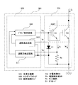
図1に示すように、第1の実施形態に係る半導体装置101は、メインデバイスチップ102と制御回路チップ103から構成される。メインデバイスチップ102には、主電流側と検出電流側でユニットセル数の比がM:1となるように並列接続された主電流側セルQMと電流検出側セルQSとで構成されたIGBTと、電流検出側セルQSに接続された電流検出抵抗のセンス抵抗RSとで構成されている。
As shown in FIG. 1, the
制御回路チップ103には、ワイヤーを介してメインデバイスチップ102内のIGBT(QMおよびQS)のゲート端子へ送る駆動信号を制御するドライブ制御回路104と、ワイヤーを介してメインデバイスチップ102内のセンス抵抗RSに電流を印加する過熱検出用電流生成回路105と、ワイヤーを介してメインデバイスチップ102内のセンス抵抗RSに生じるセンス電圧VSの値に応じて異常を検出する異常検出回路106とで構成されている。
The
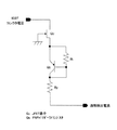
また、過熱検出用電流生成回路105は、図2に示すように、過熱検出用信号に従ってオン/オフするトランジスタQTと定電流源107とから構成される。異常検出回路106は、図3に示すように、センス電圧VSと基準電圧Vth1を比較する第1の比較器108と、センス電圧VSと基準電圧Vth2を比較する第2の比較器109と、それらの出力を処理してドライブ制御回路104に異常信号を出力する異常信号処理回路110とから構成される。なお、第1の比較器108はIGBTの過電流を検出して過電流検出信号を出力し、第2の比較器109はIGBTの過熱を検出して過熱検出信号を出力する。
Further, the overheat detecting
次に、図4に示す第1の実施形態のタイムチャートを用いて、第1の実施形態の動作を説明する。なお、図4では、IGBT(QMおよびQS)のコレクタに誘導負荷が接続され、ピーク電流を制限しながら制御を行うスイッチング電源用パワーデバイスを想定している。 Next, the operation of the first embodiment will be described using the time chart of the first embodiment shown in FIG. FIG. 4 assumes a power device for a switching power supply in which an inductive load is connected to the collector of the IGBT (Q M and Q S ) and performs control while limiting the peak current.
VGは図1で示したドライブ制御回路104の出力信号であり、IGBT(QMおよびQS)のゲート電圧である。ゲート信号VGはドライブ制御回路104から周期的に出力されるが、異常検出回路106から異常信号を受けると、ゲート信号の出力を停止し、IGBT(QMおよびQS)は遮断される。
V G is an output signal of the
ゲート信号VGがHighレベルになると、IGBT(QMおよびQS)はターンオンしてコレクタ電流ICが流れ始める。コレクタに接続された誘導負荷により、コレクタ電流ICはオン時間に伴い増加する。コレクタ電流ICのうち、電流検出側セルQSに分流したセンス電流ISも、オン時間に伴い増加するため、センス電圧VSも増加する。この時、センス電圧VSは、VS=RS×ISと表される。 When the gate signal V G becomes High level, the IGBTs (Q M and Q S ) are turned on and the collector current I C starts to flow. The inductive load connected to the collector, the collector current I C is increased with the on-time. Among the collector current I C is also the sense current I S that is shunted to the current detecting side cell Q S, in order to increase with the on-time, also increases the sense voltage V S. At this time, the sense voltage V S is expressed as V S = R S × I S.
センス電圧VSが第1の比較器108で所定の過電流検出レベル(基準電圧Vth1、例えば0.2V)と比較され、VS>Vth1となった時に、例えば、IC=10Aとなった時に、過電流検出信号が出力される。この出力は異常信号処理回路110に入力され、異常信号処理回路110は次のターンオンサイクルまで異常信号をドライブ制御回路104に出力する。IGBT(QMおよびQS)は、次のターンオンサイクルまで遮断される。すなわち、パルス毎に過電流保護によってコレクタ電流ICのピークを制限している。
When the sense voltage V S is compared with a predetermined overcurrent detection level (reference voltage Vth1, for example, 0.2V) by the
一方、ゲート信号VGがLowレベルになると、過熱検出用電流生成回路105内では、過熱検出用信号が所定の期間だけLowレベルになり、定電流(過熱検出用電流)ITがセンス抵抗RSに印加される。この時、センス電圧VSは、VS=RS×ITと表される。メインデバイスチップ102に異常な温度上昇が起きると、センス抵抗RSの抵抗値が増加し、センス電圧VSも増加する。センス電圧VSが第2の比較器109で所定の過熱検出レベル(基準電圧Vth2、例えば1.25V)と比較され、VS>Vth2となった時に、例えば、メインデバイスチップ102の温度が150℃になった時に、過熱検出信号が出力される。この出力は異常信号処理回路110に入力され、異常信号処理回路110は異常信号をドライブ制御回路104に連続して出力する。IGBT(QMおよびQS)は連続して遮断される。すなわち、過熱保護は、過電流保護とは異なり、ラッチモードで停止状態となる。
On the other hand, the gate signal V G becomes Low level, within the overheat detection
以上に述べたように、ゲート信号VGがHighレベルの期間は過電流を、ゲート信号VGがLowレベルの期間は過熱を、センス電圧VSのみモニターすることで検出することができるため、制御回路チップ103とメインデバイスチップ102のワイヤー接続を削減することができる。よって、各チップのワイヤーボンディングパッドも削減することができるため、チップ面積を有効に使うことができる。
As described above, since the period of the gate signal V G is High level overcurrent, the period of the gate signal V G is Low level overheating can be detected by monitoring only the sense voltage V S, Wire connection between the
また、センス抵抗RSをメインデバイスチップ102内に配置するため、過熱検出感度も良い。
Further, since the sense resistor RS is arranged in the
また、過電流保護と過熱保護の検出信号は共にセンス電圧VSで検出するが、各保護に対する検出レベルを変えることで、過電流検出信号と過熱検出信号の取扱いを区別し、異なる制御方法で半導体装置を保護することができる。 Although the detection signal of the overheat protection overcurrent protection detects both the sense voltage V S, by changing the detection level for each protection, to distinguish the handling of overcurrent detection signal and the overheat detection signal, in a different control method The semiconductor device can be protected.
また、過熱検出用電流ITの印加期間をゲート信号VGがLowレベルの期間の一部分のみとすることで、異常検出回路が過熱を検出するために必要な過熱検出用電流ITの印加時間が短くても良い場合に、過熱を検出するための回路消費電力を低減することができる。さらに、パワー半導体素子が導通し始める時に過熱検出用電流ITが印加されていると、誤って過電流を検出する可能性があるが、パワー半導体素子が導通し始める直前に過熱検出用電流ITの印加を停止することで誤検出を防ぐことができる。 Also, the application period of the overheat detection current I T by the gate signal V G is the only part of the duration of the Low level, the abnormality detection circuit overheating application time detection current I T required for to detect overheating In the case where it is sufficient to reduce the power consumption, the circuit power consumption for detecting overheating can be reduced. Furthermore, if the overheat detection current IT is applied when the power semiconductor element starts to conduct, there is a possibility that the overcurrent will be erroneously detected, but the overheat detection current I immediately before the power semiconductor element begins to conduct. By stopping the application of T , erroneous detection can be prevented.
なお、第1の実施形態では、電流検出側セルQSを内蔵しているIGBTで説明したが、電流検出側セルQSを備えずに、主電流が流れる母線にセンス抵抗RSを挿入し、センス抵抗RSをメインデバイスチップ102内に配置しても本発明と同様の効果を得ることができる。
In the first embodiment has been described in the IGBT has a built-in current detection side cell Q S, without providing a current detection side cell Q S, insert the sense resistor R S to the bus which main current flows Even if the sense resistor RS is arranged in the
また、第1の実施形態では、異常検出回路106での過電流検出信号と過熱検出信号の取扱いを区別し、異なる保護方法を示したが、過電流保護も過熱保護も共にラッチモードで停止させるなど、共通の保護動作にしても良い。その際には、過熱検出用電流ITの値を調整することで、第1の比較器108と第2の比較器109を統合することもできる。
In the first embodiment, the handling of the overcurrent detection signal and the overheat detection signal in the
また、第1の実施形態では、過熱検出用電流ITの印加期間をゲート信号VGがLowレベルの期間の一部分のみとしたが、ゲート信号VGがLowレベルの全期間としたり、ゲート信号VGに関係なく設定したりしても良い。 In the first embodiment, the gate signal V G to the application period of the overheat detection current I T is only a portion of the period of Low level, or the gate signal V G is the total duration of the Low level, the gate signal the V G may be or set regardless.
なお、過熱検出用電流生成回路105や異常検出回路106の回路構成は、それぞれ図2や図3に示した構成に限定されるものではない。
The circuit configurations of the overheat detection
なお、異常検出回路106には、過電流や過熱などの誤検出を防ぐためにフィルタ回路などを備えていることが望ましい。
The
また、第1の実施形態では、メインデバイスチップ102と制御回路チップ103で構成された半導体装置101を示したが、制御回路チップ103はメインデバイスチップ102と同じパッケージ内に配置されていなくても良い。
In the first embodiment, the
また、第1の実施形態では、過熱検出用電流生成回路105を制御回路チップ103内に配置しているが、過熱検出用電流生成回路105は、メインデバイスチップ102内に配置されるなど、制御回路チップ103以外に配置されていても、本発明と同様の効果を得ることができる。
In the first embodiment, the overheat detection
また、第1の実施形態では、メインデバイスを制御する回路を半導体チップ内に作製した制御回路チップ103を示したが、制御回路チップ103と同等の機能を持つ制御回路をディスクリート製品で構成しても、本発明と同様の効果を得ることができる。
In the first embodiment, the
(第2の実施形態)
以下に、本発明の第2実施形態に係る半導体装置について、図5を参照しながら説明する。図5は第2の実施形態に係る半導体装置の全体構成を示すブロック図である。なお、図1と重複する部分には同一の符号を用いており、第2の実施形態では、第1の実施形態に係る半導体装置と同様の説明は繰り返し行わない。第2の実施形態に係る半導体装置において、前述した第1の実施形態に係る半導体装置と異なる点について、具体的に説明する。
(Second Embodiment)
The semiconductor device according to the second embodiment of the present invention will be described below with reference to FIG. FIG. 5 is a block diagram showing the overall configuration of the semiconductor device according to the second embodiment. Note that the same reference numerals are used for portions that overlap those in FIG. 1, and in the second embodiment, the description similar to that of the semiconductor device according to the first embodiment is not repeated. The difference between the semiconductor device according to the second embodiment and the semiconductor device according to the first embodiment will be specifically described.
図5に示すように、第2の実施形態に係る半導体装置201においては、メインデバイスチップ202内に電流検出側セルQSとセンス抵抗RSは備えておらず、センス抵抗RSはIGBT(Q)のエミッタに外付け抵抗として接続される。また、センス抵抗RSとIGBT(Q)のエミッタとの接続点から、過熱検出用電流生成回路105と異常検出回路106との接続点までの間に、メインデバイスチップ202内に配置された温度検出用抵抗RTが挿入されている。
As shown in FIG. 5, in the
第2の実施形態に係る半導体装置によると、IGBTの導通時には、コレクタ電流IC がセンス抵抗RSに印加され、センス電圧VSは、VS=RS×ICと表される。一方で、IGBTの遮断時には、過熱検出用電流生成回路105からの過熱検出用電流ITが温度検出用抵抗RTとセンス抵抗RSに印加され、センス電圧VSは、VS=(RS+RT)×ITと表される。すなわち、過熱検出用電流ITの値が小さくてもセンス電圧VSを大きくでき、過熱を検出するための回路消費電力を低減することができる。例えば50Ωのセンス抵抗RSに対して、温度検出用抵抗RTの抵抗値を500kΩと大きく設定することで、過熱検出用電流ITを4桁小さくすることができる。ただし、温度検出用抵抗RTの抵抗値を大きくすることは、過電流の検出速度を遅らすことになるため、過電流の検出感度を考慮して設定する必要がある。
According to the semiconductor device according to a second embodiment, at the time of conduction of the IGBT, the collector current I C is applied to the sense resistor R S, the sense voltage V S is represented as V S = R S × I C . On the other hand, at the time of interruption of IGBT, overheat detection current I T from overheating detection
また、温度検出用抵抗RTの抵抗値をセンス抵抗RSに対して大きく設定することで、過熱検出感度は温度検出用抵抗RTの温度特性で支配的となり、抵抗値が温度依存性の小さい抵抗をセンス抵抗RSとして選択できる。これにより、過電流の検出レベルの温度依存性を小さくすることができる。さらには、センス抵抗RSはメインデバイスチップ202内に配置されている必要はないので、第2の実施形態のように、外付け部品としてIGBT(Q)のエミッタに接続することができる。よって、外付けの抵抗で簡単に過電流の検出レベルを変更することができる。
Further, by setting the resistance value of the temperature detection resistor RT to be larger than that of the sense resistor RS , the overheat detection sensitivity becomes dominant in the temperature characteristics of the temperature detection resistor RT , and the resistance value is temperature-dependent. A small resistance can be selected as the sense resistor RS . As a result, the temperature dependence of the overcurrent detection level can be reduced. Furthermore, since the sense resistor RS does not need to be disposed in the
なお、第2の実施形態では、センス抵抗RSを外付け抵抗としたが、メインデバイスチップ202内、または、制御回路チップ203内に配置されていても良い。その場合、温度検出用抵抗RTとは温度特性の異なる抵抗を用いても良い。
In the second embodiment, the sense resistor RS is an external resistor, but it may be arranged in the
また、第2の実施形態では、センス抵抗RSをIGBT(Q)のエミッタに直接接続した場合を示したが、メインデバイスチップ202内に電流検出側セルQSを配置して、電流検出側セルQSのエミッタにセンス抵抗RSを接続しても良い。
In the second embodiment, although the case of directly connecting a sense resistor R S to the emitter of the IGBT (Q), by arranging the current detection side cell Q S to the
(第3の実施形態)
以下に、本発明の第3の実施形態に係る半導体装置について、図6〜図8を参照しながら説明する。図6は第3の実施形態における半導体装置の全体構成を示すブロック図であり、図7は過熱検出用電流生成回路の構成を示すブロック図、図8は第3の実施形態の動作例を示すタイムチャートである。なお、図1と重複する部分には同一の符号を用いており、第3の実施形態では、第1の実施形態に係る半導体装置と同様の説明は繰り返し行わない。第3の実施形態に係る半導体装置において、前述した第1の実施形態に係る半導体装置と異なる点について、具体的に説明する。
(Third embodiment)
A semiconductor device according to the third embodiment of the present invention will be described below with reference to FIGS. FIG. 6 is a block diagram showing the overall configuration of the semiconductor device according to the third embodiment, FIG. 7 is a block diagram showing the configuration of the overheat detection current generation circuit, and FIG. 8 shows an operation example of the third embodiment. It is a time chart. Note that the same reference numerals are used for the same parts as in FIG. 1, and in the third embodiment, the description similar to that of the semiconductor device according to the first embodiment is not repeated. The difference between the semiconductor device according to the third embodiment and the semiconductor device according to the first embodiment will be specifically described.
図6に示すように、第3の実施形態に係る半導体装置301においては、過熱検出用電流生成回路305がメインデバイスチップ302内に配置されている。この過熱検出用電流生成回路305は、例えば、図7に示すように、接合型FET(JFET)素子QJと、JFET素子QJのソースに接続されるPNPバイポーラトランジスタQBと、JFET素子QJのソースとPNPバイポーラトランジスタQBのベースとの間に挿入される抵抗R1と、PNPバイポーラトランジスタQBのコレクタおよび抵抗R1に接続される抵抗R2から構成される。また、抵抗R1の抵抗値の温度依存性は抵抗R2よりも大きい。
As shown in FIG. 6, in the
なお、IGBT(QMおよびQS)が遮断してコレクタ電圧が上昇しても、JFET素子QJは所定のドレイン電圧値以上でピンチオフするように設計されており、それに伴いソース電圧は所定の値でクランプされる。図7では、ゲート端子をGNDにショートしたノーマリーオン型JFET素子QJを示しており、例えば、50V以上のドレイン電圧が印加されても、ソース電圧は50V以下でクランプされる。JFET素子QJのドレイン端子はIGBT(QMおよびQS)のコレクタ端子と接続されており、IGBT(QMおよびQS)が遮断してコレクタ電圧が高電位になった時にクランプされたJFET素子QJのソース電圧は、抵抗R1と抵抗R2で分圧される。 Even if the IGBT (Q M and Q S ) is cut off and the collector voltage rises, the JFET element Q J is designed to pinch off at a predetermined drain voltage value or higher, and accordingly, the source voltage is set to a predetermined value. Clamped by value. 7 shows the normally-on type JFET device Q J a short circuit of the gate terminal to GND, the example, be applied over the drain voltage 50V, source voltage is clamped at 50V or less. The drain terminal of JFET element Q J is connected to the collector terminal of the IGBT (Q M and Q S), IGBT (Q M and Q S) is clamped when the collector voltage is cut off becomes a high potential JFET the source voltage of the device Q J is divided by resistors R 1 and R 2 minute.
温度が上昇すると、抵抗R1と抵抗R2の温度特性の違いにより、分圧比が変化する。また、温度上昇に伴い、PNPバイポーラトランジスタQBの閾値電圧(室温で約0.7V)も低下する。これらの温度特性を考慮して抵抗R1と抵抗R2の分圧比を設定することで、所望の温度に達した時に、PNPバイポーラトランジスタQBのベース−エミッタ間に閾値電圧以上の電圧差が生じて、センス抵抗RSに流れる電流が急増する。異常検出回路106は、センス電圧VSの急増から過熱を検出する。また、センス抵抗RSは半導体装置内に配置せず、外付け抵抗として電流検出側セルQSに接続されている。
As the temperature increases, the difference in temperature characteristics of the resistors R 1 and R 2, partial pressure ratio is changed. Further, as the temperature rises, the threshold voltage (about 0.7V at room temperature) of the PNP bipolar transistor Q B also decreases. By taking into account these temperature characteristics setting the division ratio of the resistors R 1 and R 2, when the desired temperature has been reached, the base of the PNP bipolar transistor Q B - voltage difference above the threshold voltage between the emitter As a result, the current flowing through the sense resistor RS increases rapidly. The
第3の実施形態に係る半導体装置によると、過熱検出用電流生成回路305は、メインデバイスチップ302内に配置されており、制御回路チップ303内には、過熱を検出するための回路としてセンス電圧VSを基準電圧と比較するような比較器などがあれば良く、制御回路の構成が簡単になる。または、過熱検出用電流生成回路305からの過熱検出用電流を調整して、過熱と過電流とを検出する比較器を統合することで、制御回路チップ303は従来の汎用品を利用することもできる。
According to the semiconductor device of the third embodiment, the overheat detection
また、第3の実施形態に係る半導体装置によると、センス抵抗RSはメインデバイスチップ302内に配置されている必要はないので、外付け部品として電流検出側セルQSに接続することができる。よって、外付け抵抗で簡単に過電流の検出レベルを変更することができる。
Further, in the semiconductor device according to the third embodiment, the sense resistor R S so need not be located in the
また、第3の実施形態に係る半導体装置によると、IGBT(QMおよびQS)のコレクタ端子に接続されたJFET素子QJを利用することで、IGBT(QMおよびQS)のコレクタ電圧が所定値以上であれば、コレクタ電圧に依存しないクランプ電圧を過熱検出用電流生成回路305内の定電圧源とすることができ、過熱検出用電流生成回路305の電源電圧を、メインデバイスチップ302の外部から供給したり、メインデバイスチップ302内で生成したりする必要がなくなる。さらに、JFET素子QJのクランプ電圧の設定値を低く抑えることで、JFET素子QJのソース端子に接続される回路素子の端子電圧定格を小さくすることができる。
Further, in the semiconductor device according to the third embodiment, the collector voltage of the IGBT by using the (Q M and Q S) JFET device Q J connected to the collector terminal of, IGBT (Q M and Q S) Can be used as a constant voltage source in the overheat detection
なお、第3の実施形態では、センス抵抗RSを外付け抵抗としたが、メインデバイスチップ302内、または制御回路チップ303内に配置されていても良い。
In the third embodiment, the sense resistor RS is an external resistor. However, the sense resistor RS may be disposed in the
また、過熱検出用電流生成回路305の回路構成は、図7に示す構成に限定されるものではない。メインデバイスチップ302の過熱時、またはその温度に応じて、センス抵抗RSに電流を流す回路構成にすることで、本発明と同様の効果を得ることができる。
Further, the circuit configuration of the overheat detection
また、第3の実施形態の過熱検出用電流生成回路305では、JFET素子QJを用いて過熱検出用電流生成回路305の電力を供給しているが、IGBT(QMおよびQS)を駆動するためのゲート電圧を利用して過熱検出用電流生成回路305の回路電力を供給するなどの構成にしても良い。
Further, in the third embodiment of the overheat detecting
以上のように、第1〜第3の実施形態では、本発明に係る半導体装置において、過熱と過電流をセンス電圧のみで検出する方法について紹介したが、この他にも本発明の主旨を逸脱しない範囲での半導体装置構成を含むことは言うまでもない。 As described above, in the first to third embodiments, the method of detecting overheating and overcurrent only by the sense voltage in the semiconductor device according to the present invention has been introduced, but other than this, it deviates from the gist of the present invention. It goes without saying that the semiconductor device configuration in a range not to be included is included.
本発明に係る半導体装置は、パワー半導体素子の過電流を検出するセンス電圧のみモニターすることで、同時にパワー半導体素子の過熱を検出することができ、制御回路チップとメインデバイスチップのワイヤー接続を削減して、ワイヤー接続のコスト削減およびチップ面積を有効利用が可能となって、より性能の良い半導体装置を提供することができる。 The semiconductor device according to the present invention can detect the overheating of the power semiconductor element at the same time by monitoring only the sense voltage for detecting the overcurrent of the power semiconductor element, and reduces the wire connection between the control circuit chip and the main device chip. Thus, the cost of wire connection and the chip area can be effectively used, and a semiconductor device with better performance can be provided.
101,201,301,501 半導体装置
102,202,302,502 メインデバイスチップ
103,203,303,503 制御回路チップ
104,504 ドライブ制御回路
105,305 過熱検出用電流生成回路
106 異常検出回路
107 定電流源
108 第1の比較器
109 第2の比較器
110 異常信号処理回路
511 過電流検出回路
512 過熱検出回路
101, 201, 301, 501
Claims (9)
Priority Applications (1)
| Application Number | Priority Date | Filing Date | Title |
|---|---|---|---|
| JP2008001219A JP2009165285A (en) | 2008-01-08 | 2008-01-08 | Semiconductor device |
Applications Claiming Priority (1)
| Application Number | Priority Date | Filing Date | Title |
|---|---|---|---|
| JP2008001219A JP2009165285A (en) | 2008-01-08 | 2008-01-08 | Semiconductor device |
Publications (1)
| Publication Number | Publication Date |
|---|---|
| JP2009165285A true JP2009165285A (en) | 2009-07-23 |
Family
ID=40967240
Family Applications (1)
| Application Number | Title | Priority Date | Filing Date |
|---|---|---|---|
| JP2008001219A Pending JP2009165285A (en) | 2008-01-08 | 2008-01-08 | Semiconductor device |
Country Status (1)
| Country | Link |
|---|---|
| JP (1) | JP2009165285A (en) |
Cited By (7)
| Publication number | Priority date | Publication date | Assignee | Title |
|---|---|---|---|---|
| WO2012029652A1 (en) * | 2010-09-03 | 2012-03-08 | 三菱電機株式会社 | Semiconductor device |
| CN103460367A (en) * | 2011-04-04 | 2013-12-18 | 富士电机株式会社 | Wafer testing method for power switch |
| JP2018129969A (en) * | 2017-02-10 | 2018-08-16 | サンケン電気株式会社 | Electronic circuit and overheat detection method |
| CN111034044A (en) * | 2017-08-30 | 2020-04-17 | 矢崎总业株式会社 | Semiconductor relay and current detection device for vehicle |
| JP2020532275A (en) * | 2017-09-30 | 2020-11-05 | 深▲セン▼市▲華▼星光▲電▼半▲導▼体▲顕▼示技▲術▼有限公司 | Liquid crystal display panel and switching control circuit |
| KR102219433B1 (en) * | 2019-11-26 | 2021-02-24 | 현대모비스 주식회사 | Over current detection circuit for power semiconductor |
| WO2023199840A1 (en) * | 2022-04-11 | 2023-10-19 | 富士電機株式会社 | Semiconductor device and overcurrent protection device |
-
2008
- 2008-01-08 JP JP2008001219A patent/JP2009165285A/en active Pending
Cited By (13)
| Publication number | Priority date | Publication date | Assignee | Title |
|---|---|---|---|---|
| WO2012029652A1 (en) * | 2010-09-03 | 2012-03-08 | 三菱電機株式会社 | Semiconductor device |
| CN103098198A (en) * | 2010-09-03 | 2013-05-08 | 三菱电机株式会社 | Semiconductor device |
| JP5372257B2 (en) * | 2010-09-03 | 2013-12-18 | 三菱電機株式会社 | Semiconductor device |
| US8785931B2 (en) | 2010-09-03 | 2014-07-22 | Mitsubishi Electric Corporation | Semiconductor device |
| CN103460367A (en) * | 2011-04-04 | 2013-12-18 | 富士电机株式会社 | Wafer testing method for power switch |
| US9541599B2 (en) | 2011-04-04 | 2017-01-10 | Fuji Electric Co., Ltd. | Power switch wafer test method |
| JP2018129969A (en) * | 2017-02-10 | 2018-08-16 | サンケン電気株式会社 | Electronic circuit and overheat detection method |
| CN111034044A (en) * | 2017-08-30 | 2020-04-17 | 矢崎总业株式会社 | Semiconductor relay and current detection device for vehicle |
| CN111034044B (en) * | 2017-08-30 | 2023-04-18 | 矢崎总业株式会社 | Semiconductor relay and current detection device for vehicle |
| JP2020532275A (en) * | 2017-09-30 | 2020-11-05 | 深▲セン▼市▲華▼星光▲電▼半▲導▼体▲顕▼示技▲術▼有限公司 | Liquid crystal display panel and switching control circuit |
| JP7150019B2 (en) | 2017-09-30 | 2022-10-07 | 深▲セン▼市▲華▼星光▲電▼半▲導▼体▲顕▼示技▲術▼有限公司 | Liquid crystal display panel and its power on/off switching control circuit |
| KR102219433B1 (en) * | 2019-11-26 | 2021-02-24 | 현대모비스 주식회사 | Over current detection circuit for power semiconductor |
| WO2023199840A1 (en) * | 2022-04-11 | 2023-10-19 | 富士電機株式会社 | Semiconductor device and overcurrent protection device |
Similar Documents
| Publication | Publication Date | Title |
|---|---|---|
| JP7038758B2 (en) | Semiconductor devices and electronic circuits containing them | |
| US9628067B2 (en) | Gate driver | |
| CN107615664B (en) | Power transistor driving device | |
| US7414867B2 (en) | Power conversion device | |
| US8848330B2 (en) | Circuit with a temperature protected electronic switch | |
| JP7305303B2 (en) | drive and power module | |
| US8264256B2 (en) | Driver and method for driving a device | |
| JP2009165285A (en) | Semiconductor device | |
| JP5940211B2 (en) | Semiconductor device | |
| JP5974548B2 (en) | Semiconductor device | |
| JP2013106464A (en) | Semiconductor device | |
| US9720029B2 (en) | Semiconductor device including a sense element and a main element, and current detector circuit using the semiconductor device | |
| JP2009171842A (en) | Power conversion apparatus | |
| US8570780B2 (en) | Semiconductor device | |
| JP4920319B2 (en) | Semiconductor device lifetime prediction circuit | |
| JP2014138521A (en) | Driving device for semiconductor element | |
| WO2016039342A1 (en) | Semiconductor module | |
| JP6107949B2 (en) | Semiconductor module | |
| JP5360304B2 (en) | Semiconductor device | |
| JP5325437B2 (en) | Integrated circuit | |
| US11462445B2 (en) | Semiconductor module and semiconductor-module deterioration detecting method | |
| JP5790606B2 (en) | Overheat protection circuit | |
| JP6168899B2 (en) | Power module | |
| JP2017108244A (en) | Control circuit for semiconductor device | |
| JP2023169458A (en) | Semiconductor device |
Legal Events
| Date | Code | Title | Description |
|---|---|---|---|
| RD03 | Notification of appointment of power of attorney |
Free format text: JAPANESE INTERMEDIATE CODE: A7423 Effective date: 20100910 |
|
| RD04 | Notification of resignation of power of attorney |
Free format text: JAPANESE INTERMEDIATE CODE: A7424 Effective date: 20100915 |