JP2009135464A - Method of manufacturing photoelectric converter - Google Patents
Method of manufacturing photoelectric converter Download PDFInfo
- Publication number
- JP2009135464A JP2009135464A JP2008277605A JP2008277605A JP2009135464A JP 2009135464 A JP2009135464 A JP 2009135464A JP 2008277605 A JP2008277605 A JP 2008277605A JP 2008277605 A JP2008277605 A JP 2008277605A JP 2009135464 A JP2009135464 A JP 2009135464A
- Authority
- JP
- Japan
- Prior art keywords
- single crystal
- semiconductor layer
- crystal semiconductor
- layer
- electrode
- Prior art date
- Legal status (The legal status is an assumption and is not a legal conclusion. Google has not performed a legal analysis and makes no representation as to the accuracy of the status listed.)
- Withdrawn
Links
- 238000004519 manufacturing process Methods 0.000 title claims abstract description 56
- 239000004065 semiconductor Substances 0.000 claims abstract description 335
- 239000000758 substrate Substances 0.000 claims abstract description 229
- 239000013078 crystal Substances 0.000 claims abstract description 197
- 238000006243 chemical reaction Methods 0.000 claims abstract description 76
- 238000000926 separation method Methods 0.000 claims abstract description 12
- 239000012535 impurity Substances 0.000 claims description 106
- 150000002500 ions Chemical class 0.000 claims description 56
- 229910052739 hydrogen Inorganic materials 0.000 claims description 43
- 239000001257 hydrogen Substances 0.000 claims description 43
- 238000000034 method Methods 0.000 claims description 40
- UFHFLCQGNIYNRP-UHFFFAOYSA-N Hydrogen Chemical compound [H][H] UFHFLCQGNIYNRP-UHFFFAOYSA-N 0.000 claims description 31
- 239000011521 glass Substances 0.000 claims description 19
- 238000010884 ion-beam technique Methods 0.000 claims description 19
- 238000010438 heat treatment Methods 0.000 claims description 18
- 230000001678 irradiating effect Effects 0.000 claims description 11
- 239000012299 nitrogen atmosphere Substances 0.000 claims description 4
- GPRLSGONYQIRFK-UHFFFAOYSA-N hydron Chemical compound [H+] GPRLSGONYQIRFK-UHFFFAOYSA-N 0.000 claims 1
- 239000010410 layer Substances 0.000 abstract description 268
- XUIMIQQOPSSXEZ-UHFFFAOYSA-N Silicon Chemical compound [Si] XUIMIQQOPSSXEZ-UHFFFAOYSA-N 0.000 abstract description 31
- 229910052710 silicon Inorganic materials 0.000 abstract description 31
- 239000010703 silicon Substances 0.000 abstract description 31
- 239000002344 surface layer Substances 0.000 abstract description 13
- 239000000463 material Substances 0.000 abstract description 10
- 238000009413 insulation Methods 0.000 abstract description 2
- 239000010408 film Substances 0.000 description 74
- 239000007789 gas Substances 0.000 description 45
- 230000001681 protective effect Effects 0.000 description 23
- IJGRMHOSHXDMSA-UHFFFAOYSA-N Atomic nitrogen Chemical compound N#N IJGRMHOSHXDMSA-UHFFFAOYSA-N 0.000 description 19
- 229910052581 Si3N4 Inorganic materials 0.000 description 19
- HQVNEWCFYHHQES-UHFFFAOYSA-N silicon nitride Chemical compound N12[Si]34N5[Si]62N3[Si]51N64 HQVNEWCFYHHQES-UHFFFAOYSA-N 0.000 description 19
- 238000013532 laser treatment Methods 0.000 description 17
- 238000010248 power generation Methods 0.000 description 17
- 235000012431 wafers Nutrition 0.000 description 16
- 230000007547 defect Effects 0.000 description 15
- 230000008569 process Effects 0.000 description 15
- 239000012790 adhesive layer Substances 0.000 description 13
- 230000015572 biosynthetic process Effects 0.000 description 11
- 238000005520 cutting process Methods 0.000 description 11
- 238000002347 injection Methods 0.000 description 11
- 239000007924 injection Substances 0.000 description 11
- 238000005530 etching Methods 0.000 description 10
- 230000008439 repair process Effects 0.000 description 9
- 230000000694 effects Effects 0.000 description 8
- VYPSYNLAJGMNEJ-UHFFFAOYSA-N Silicium dioxide Chemical compound O=[Si]=O VYPSYNLAJGMNEJ-UHFFFAOYSA-N 0.000 description 7
- 229910001873 dinitrogen Inorganic materials 0.000 description 7
- -1 hydrogen ions Chemical class 0.000 description 7
- 229910021421 monocrystalline silicon Inorganic materials 0.000 description 7
- 229910021420 polycrystalline silicon Inorganic materials 0.000 description 7
- 229910052814 silicon oxide Inorganic materials 0.000 description 7
- QVGXLLKOCUKJST-UHFFFAOYSA-N atomic oxygen Chemical compound [O] QVGXLLKOCUKJST-UHFFFAOYSA-N 0.000 description 6
- 239000000969 carrier Substances 0.000 description 6
- 229910052757 nitrogen Inorganic materials 0.000 description 6
- 229910052760 oxygen Inorganic materials 0.000 description 6
- 239000001301 oxygen Substances 0.000 description 6
- 238000005268 plasma chemical vapour deposition Methods 0.000 description 6
- 125000004429 atom Chemical group 0.000 description 5
- 230000003287 optical effect Effects 0.000 description 5
- 238000003860 storage Methods 0.000 description 5
- 239000010409 thin film Substances 0.000 description 5
- BLRPTPMANUNPDV-UHFFFAOYSA-N Silane Chemical compound [SiH4] BLRPTPMANUNPDV-UHFFFAOYSA-N 0.000 description 4
- BQCADISMDOOEFD-UHFFFAOYSA-N Silver Chemical compound [Ag] BQCADISMDOOEFD-UHFFFAOYSA-N 0.000 description 4
- 238000005229 chemical vapour deposition Methods 0.000 description 4
- 238000002425 crystallisation Methods 0.000 description 4
- 230000008025 crystallization Effects 0.000 description 4
- 238000001312 dry etching Methods 0.000 description 4
- 150000002431 hydrogen Chemical class 0.000 description 4
- 230000008018 melting Effects 0.000 description 4
- 238000002844 melting Methods 0.000 description 4
- 239000007769 metal material Substances 0.000 description 4
- 230000002265 prevention Effects 0.000 description 4
- 229910000077 silane Inorganic materials 0.000 description 4
- 229910052709 silver Inorganic materials 0.000 description 4
- 239000004332 silver Substances 0.000 description 4
- 230000004888 barrier function Effects 0.000 description 3
- 230000015556 catabolic process Effects 0.000 description 3
- 238000001816 cooling Methods 0.000 description 3
- 238000001678 elastic recoil detection analysis Methods 0.000 description 3
- 230000005684 electric field Effects 0.000 description 3
- 230000005660 hydrophilic surface Effects 0.000 description 3
- 229910052751 metal Inorganic materials 0.000 description 3
- 239000002184 metal Substances 0.000 description 3
- 150000004767 nitrides Chemical class 0.000 description 3
- 238000002161 passivation Methods 0.000 description 3
- 230000002093 peripheral effect Effects 0.000 description 3
- 238000005001 rutherford backscattering spectroscopy Methods 0.000 description 3
- 239000007787 solid Substances 0.000 description 3
- 230000003746 surface roughness Effects 0.000 description 3
- WZJUBBHODHNQPW-UHFFFAOYSA-N 2,4,6,8-tetramethyl-1,3,5,7,2$l^{3},4$l^{3},6$l^{3},8$l^{3}-tetraoxatetrasilocane Chemical compound C[Si]1O[Si](C)O[Si](C)O[Si](C)O1 WZJUBBHODHNQPW-UHFFFAOYSA-N 0.000 description 2
- QGZKDVFQNNGYKY-UHFFFAOYSA-N Ammonia Chemical compound N QGZKDVFQNNGYKY-UHFFFAOYSA-N 0.000 description 2
- XKRFYHLGVUSROY-UHFFFAOYSA-N Argon Chemical compound [Ar] XKRFYHLGVUSROY-UHFFFAOYSA-N 0.000 description 2
- ZOXJGFHDIHLPTG-UHFFFAOYSA-N Boron Chemical compound [B] ZOXJGFHDIHLPTG-UHFFFAOYSA-N 0.000 description 2
- GQPLMRYTRLFLPF-UHFFFAOYSA-N Nitrous Oxide Chemical compound [O-][N+]#N GQPLMRYTRLFLPF-UHFFFAOYSA-N 0.000 description 2
- OAICVXFJPJFONN-UHFFFAOYSA-N Phosphorus Chemical compound [P] OAICVXFJPJFONN-UHFFFAOYSA-N 0.000 description 2
- BOTDANWDWHJENH-UHFFFAOYSA-N Tetraethyl orthosilicate Chemical compound CCO[Si](OCC)(OCC)OCC BOTDANWDWHJENH-UHFFFAOYSA-N 0.000 description 2
- 230000002411 adverse Effects 0.000 description 2
- 229910052782 aluminium Inorganic materials 0.000 description 2
- XAGFODPZIPBFFR-UHFFFAOYSA-N aluminium Chemical compound [Al] XAGFODPZIPBFFR-UHFFFAOYSA-N 0.000 description 2
- 238000004458 analytical method Methods 0.000 description 2
- 229910052785 arsenic Inorganic materials 0.000 description 2
- RQNWIZPPADIBDY-UHFFFAOYSA-N arsenic atom Chemical compound [As] RQNWIZPPADIBDY-UHFFFAOYSA-N 0.000 description 2
- 239000012298 atmosphere Substances 0.000 description 2
- 229910052796 boron Inorganic materials 0.000 description 2
- 229910021419 crystalline silicon Inorganic materials 0.000 description 2
- 238000000151 deposition Methods 0.000 description 2
- 230000008021 deposition Effects 0.000 description 2
- 238000010586 diagram Methods 0.000 description 2
- 238000007667 floating Methods 0.000 description 2
- 239000011261 inert gas Substances 0.000 description 2
- 238000005304 joining Methods 0.000 description 2
- LQBJWKCYZGMFEV-UHFFFAOYSA-N lead tin Chemical compound [Sn].[Pb] LQBJWKCYZGMFEV-UHFFFAOYSA-N 0.000 description 2
- 239000000203 mixture Substances 0.000 description 2
- 150000001282 organosilanes Chemical class 0.000 description 2
- 230000010355 oscillation Effects 0.000 description 2
- 229910052698 phosphorus Inorganic materials 0.000 description 2
- 239000011574 phosphorus Substances 0.000 description 2
- 239000003870 refractory metal Substances 0.000 description 2
- 238000007650 screen-printing Methods 0.000 description 2
- 125000005372 silanol group Chemical group 0.000 description 2
- 229910021332 silicide Inorganic materials 0.000 description 2
- FVBUAEGBCNSCDD-UHFFFAOYSA-N silicide(4-) Chemical compound [Si-4] FVBUAEGBCNSCDD-UHFFFAOYSA-N 0.000 description 2
- 229910000679 solder Inorganic materials 0.000 description 2
- 239000000126 substance Substances 0.000 description 2
- CZDYPVPMEAXLPK-UHFFFAOYSA-N tetramethylsilane Chemical compound C[Si](C)(C)C CZDYPVPMEAXLPK-UHFFFAOYSA-N 0.000 description 2
- 230000032258 transport Effects 0.000 description 2
- 239000002699 waste material Substances 0.000 description 2
- XLYOFNOQVPJJNP-UHFFFAOYSA-N water Substances O XLYOFNOQVPJJNP-UHFFFAOYSA-N 0.000 description 2
- 238000001039 wet etching Methods 0.000 description 2
- VYZAMTAEIAYCRO-UHFFFAOYSA-N Chromium Chemical compound [Cr] VYZAMTAEIAYCRO-UHFFFAOYSA-N 0.000 description 1
- ZOKXTWBITQBERF-UHFFFAOYSA-N Molybdenum Chemical compound [Mo] ZOKXTWBITQBERF-UHFFFAOYSA-N 0.000 description 1
- 229910002656 O–Si–O Inorganic materials 0.000 description 1
- 229910008051 Si-OH Inorganic materials 0.000 description 1
- 229910006358 Si—OH Inorganic materials 0.000 description 1
- RTAQQCXQSZGOHL-UHFFFAOYSA-N Titanium Chemical compound [Ti] RTAQQCXQSZGOHL-UHFFFAOYSA-N 0.000 description 1
- 238000005411 Van der Waals force Methods 0.000 description 1
- 230000001133 acceleration Effects 0.000 description 1
- 230000004913 activation Effects 0.000 description 1
- 230000001154 acute effect Effects 0.000 description 1
- 239000000853 adhesive Substances 0.000 description 1
- 230000001070 adhesive effect Effects 0.000 description 1
- 239000005407 aluminoborosilicate glass Substances 0.000 description 1
- 239000005354 aluminosilicate glass Substances 0.000 description 1
- 229910052786 argon Inorganic materials 0.000 description 1
- 238000001505 atmospheric-pressure chemical vapour deposition Methods 0.000 description 1
- 229910052788 barium Inorganic materials 0.000 description 1
- DSAJWYNOEDNPEQ-UHFFFAOYSA-N barium atom Chemical compound [Ba] DSAJWYNOEDNPEQ-UHFFFAOYSA-N 0.000 description 1
- 238000005452 bending Methods 0.000 description 1
- 238000007664 blowing Methods 0.000 description 1
- 239000005388 borosilicate glass Substances 0.000 description 1
- 239000003990 capacitor Substances 0.000 description 1
- 239000000919 ceramic Substances 0.000 description 1
- 230000008859 change Effects 0.000 description 1
- 229910052804 chromium Inorganic materials 0.000 description 1
- 239000011651 chromium Substances 0.000 description 1
- 238000011109 contamination Methods 0.000 description 1
- 238000007599 discharging Methods 0.000 description 1
- KPUWHANPEXNPJT-UHFFFAOYSA-N disiloxane Chemical class [SiH3]O[SiH3] KPUWHANPEXNPJT-UHFFFAOYSA-N 0.000 description 1
- 239000002019 doping agent Substances 0.000 description 1
- 238000010891 electric arc Methods 0.000 description 1
- 238000005401 electroluminescence Methods 0.000 description 1
- 238000000605 extraction Methods 0.000 description 1
- FFUAGWLWBBFQJT-UHFFFAOYSA-N hexamethyldisilazane Chemical compound C[Si](C)(C)N[Si](C)(C)C FFUAGWLWBBFQJT-UHFFFAOYSA-N 0.000 description 1
- 125000002887 hydroxy group Chemical group [H]O* 0.000 description 1
- 230000001771 impaired effect Effects 0.000 description 1
- 239000004973 liquid crystal related substance Substances 0.000 description 1
- 238000004518 low pressure chemical vapour deposition Methods 0.000 description 1
- 229910052750 molybdenum Inorganic materials 0.000 description 1
- 239000011733 molybdenum Substances 0.000 description 1
- 230000007935 neutral effect Effects 0.000 description 1
- 239000001272 nitrous oxide Substances 0.000 description 1
- 239000002994 raw material Substances 0.000 description 1
- 238000005215 recombination Methods 0.000 description 1
- 230000006798 recombination Effects 0.000 description 1
- 239000002210 silicon-based material Substances 0.000 description 1
- 239000007921 spray Substances 0.000 description 1
- 238000003892 spreading Methods 0.000 description 1
- 230000007480 spreading Effects 0.000 description 1
- 238000004544 sputter deposition Methods 0.000 description 1
- 238000004381 surface treatment Methods 0.000 description 1
- 229910052719 titanium Inorganic materials 0.000 description 1
- 239000010936 titanium Substances 0.000 description 1
- 238000011282 treatment Methods 0.000 description 1
- QQQSFSZALRVCSZ-UHFFFAOYSA-N triethoxysilane Chemical compound CCO[SiH](OCC)OCC QQQSFSZALRVCSZ-UHFFFAOYSA-N 0.000 description 1
- WFKWXMTUELFFGS-UHFFFAOYSA-N tungsten Chemical compound [W] WFKWXMTUELFFGS-UHFFFAOYSA-N 0.000 description 1
- 229910052721 tungsten Inorganic materials 0.000 description 1
- 239000010937 tungsten Substances 0.000 description 1
- 238000001771 vacuum deposition Methods 0.000 description 1
- 238000010792 warming Methods 0.000 description 1
Images


Classifications
-
- H—ELECTRICITY
- H01—ELECTRIC ELEMENTS
- H01L—SEMICONDUCTOR DEVICES NOT COVERED BY CLASS H10
- H01L31/00—Semiconductor devices sensitive to infrared radiation, light, electromagnetic radiation of shorter wavelength or corpuscular radiation and specially adapted either for the conversion of the energy of such radiation into electrical energy or for the control of electrical energy by such radiation; Processes or apparatus specially adapted for the manufacture or treatment thereof or of parts thereof; Details thereof
- H01L31/18—Processes or apparatus specially adapted for the manufacture or treatment of these devices or of parts thereof
- H01L31/1804—Processes or apparatus specially adapted for the manufacture or treatment of these devices or of parts thereof comprising only elements of Group IV of the Periodic System
-
- H—ELECTRICITY
- H01—ELECTRIC ELEMENTS
- H01L—SEMICONDUCTOR DEVICES NOT COVERED BY CLASS H10
- H01L21/00—Processes or apparatus adapted for the manufacture or treatment of semiconductor or solid state devices or of parts thereof
- H01L21/70—Manufacture or treatment of devices consisting of a plurality of solid state components formed in or on a common substrate or of parts thereof; Manufacture of integrated circuit devices or of parts thereof
- H01L21/71—Manufacture of specific parts of devices defined in group H01L21/70
- H01L21/76—Making of isolation regions between components
- H01L21/762—Dielectric regions, e.g. EPIC dielectric isolation, LOCOS; Trench refilling techniques, SOI technology, use of channel stoppers
- H01L21/7624—Dielectric regions, e.g. EPIC dielectric isolation, LOCOS; Trench refilling techniques, SOI technology, use of channel stoppers using semiconductor on insulator [SOI] technology
- H01L21/76251—Dielectric regions, e.g. EPIC dielectric isolation, LOCOS; Trench refilling techniques, SOI technology, use of channel stoppers using semiconductor on insulator [SOI] technology using bonding techniques
- H01L21/76254—Dielectric regions, e.g. EPIC dielectric isolation, LOCOS; Trench refilling techniques, SOI technology, use of channel stoppers using semiconductor on insulator [SOI] technology using bonding techniques with separation/delamination along an ion implanted layer, e.g. Smart-cut, Unibond
-
- H—ELECTRICITY
- H01—ELECTRIC ELEMENTS
- H01L—SEMICONDUCTOR DEVICES NOT COVERED BY CLASS H10
- H01L31/00—Semiconductor devices sensitive to infrared radiation, light, electromagnetic radiation of shorter wavelength or corpuscular radiation and specially adapted either for the conversion of the energy of such radiation into electrical energy or for the control of electrical energy by such radiation; Processes or apparatus specially adapted for the manufacture or treatment thereof or of parts thereof; Details thereof
- H01L31/18—Processes or apparatus specially adapted for the manufacture or treatment of these devices or of parts thereof
- H01L31/1892—Processes or apparatus specially adapted for the manufacture or treatment of these devices or of parts thereof methods involving the use of temporary, removable substrates
-
- Y—GENERAL TAGGING OF NEW TECHNOLOGICAL DEVELOPMENTS; GENERAL TAGGING OF CROSS-SECTIONAL TECHNOLOGIES SPANNING OVER SEVERAL SECTIONS OF THE IPC; TECHNICAL SUBJECTS COVERED BY FORMER USPC CROSS-REFERENCE ART COLLECTIONS [XRACs] AND DIGESTS
- Y02—TECHNOLOGIES OR APPLICATIONS FOR MITIGATION OR ADAPTATION AGAINST CLIMATE CHANGE
- Y02E—REDUCTION OF GREENHOUSE GAS [GHG] EMISSIONS, RELATED TO ENERGY GENERATION, TRANSMISSION OR DISTRIBUTION
- Y02E10/00—Energy generation through renewable energy sources
- Y02E10/50—Photovoltaic [PV] energy
- Y02E10/547—Monocrystalline silicon PV cells
-
- Y—GENERAL TAGGING OF NEW TECHNOLOGICAL DEVELOPMENTS; GENERAL TAGGING OF CROSS-SECTIONAL TECHNOLOGIES SPANNING OVER SEVERAL SECTIONS OF THE IPC; TECHNICAL SUBJECTS COVERED BY FORMER USPC CROSS-REFERENCE ART COLLECTIONS [XRACs] AND DIGESTS
- Y02—TECHNOLOGIES OR APPLICATIONS FOR MITIGATION OR ADAPTATION AGAINST CLIMATE CHANGE
- Y02P—CLIMATE CHANGE MITIGATION TECHNOLOGIES IN THE PRODUCTION OR PROCESSING OF GOODS
- Y02P70/00—Climate change mitigation technologies in the production process for final industrial or consumer products
- Y02P70/50—Manufacturing or production processes characterised by the final manufactured product
Abstract
Description
本発明は、半導体層を用いた光電変換装置の製造方法に関する。特に、単結晶半導体層を用いた光電変換装置の製造方法に関する。 The present invention relates to a method for manufacturing a photoelectric conversion device using a semiconductor layer. In particular, the present invention relates to a method for manufacturing a photoelectric conversion device using a single crystal semiconductor layer.
地球温暖化防止対策として、世界各国で太陽光発電の普及が進んでいる。例えば、2005年における太陽電池の全世界生産量は1759MWであり、前年度に比べて147%増加している。普及が進んでいる太陽電池としては結晶系太陽電池があり、単結晶シリコンを用いた太陽電池又は多結晶シリコンを用いた太陽電池が生産量の大部分を占めている。これらの太陽電池は、大型のシリコンインゴットを輪切りにして製造されるシリコンウエハを基体として用いている。 As a global warming prevention measure, photovoltaic power generation is spreading all over the world. For example, the global production of solar cells in 2005 is 1759 MW, an increase of 147% compared to the previous year. As a solar cell which has been widely used, there is a crystalline solar cell, and a solar cell using single crystal silicon or a solar cell using polycrystalline silicon occupies most of the production amount. These solar cells use, as a base, a silicon wafer manufactured by cutting a large silicon ingot.
シリコンを材料とする結晶系太陽電池は、太陽光を吸収するために10μm程度の厚さがあれば十分であるが、実際のシリコンウエハは200μmから300μm程度の厚さを有している。つまり、結晶系太陽電池では光電変換に必要な厚さよりも10倍以上厚く形成されていることになり、シリコンウエハを有効利用しているとは言い難い状況にある。極端に言えば、シリコンウエハの殆どは太陽電池の形状を維持するための構造体として機能しているにすぎないのである。 A crystalline solar cell made of silicon is sufficient if it has a thickness of about 10 μm to absorb sunlight, but an actual silicon wafer has a thickness of about 200 μm to 300 μm. That is, the crystalline solar cell is formed to be 10 times thicker than the thickness necessary for photoelectric conversion, and it is difficult to say that the silicon wafer is effectively used. Extremely speaking, most silicon wafers only function as a structure for maintaining the shape of the solar cell.
太陽電池の生産量が年々増加するにつれ、シリコンの原料である多結晶シリコンの供給不足と、それによるシリコンウエハの価格の高騰が産業界の問題となっている。2007年の多結晶シリコンの生産量は約36000トンが見込まれているのに対し、半導体(LSI)向けに25000トン以上、太陽電池用に20000トン以上が必要とされ、約10000トンの供給不足になると見込まれている。そして、このような供給不足は今後も続くものと予想されている。 As the production of solar cells increases year by year, the shortage of supply of polycrystalline silicon, which is a raw material for silicon, and the resulting increase in the price of silicon wafers have become a problem for the industry. Polycrystalline silicon production in 2007 is expected to be about 36,000 tons, but 25,000 tons or more for semiconductors (LSI) and 20,000 tons for solar cells are required, and there is a shortage of about 10,000 tons It is expected to become. And such a supply shortage is expected to continue.
尤も、このような状況を予想して、これまで結晶系薄膜シリコン太陽電池の開発が進められてきた。例えば、プラズマCVD法で、27MHz以上のVHF周波数を用い、これをさらにパルス変調して結晶性シリコン膜を基板上に堆積するシリコン薄膜太陽電池の製造方法が開示されている(特許文献1参照)。また、テクスチャー電極と呼ばれる微細な凹凸形状を持った特殊な電極の上に、多結晶シリコン薄膜をプラズマCVD法で成膜するときに、結晶粒と結晶粒界へのドーパントの添加を最適化するために、プラズマ処理条件を制御する技術が開示されている(特許文献2参照)。
しかしながら、結晶系薄膜シリコン太陽電池は単結晶シリコン太陽電池に比べて結晶の質が悪く、光電変換特性が依然劣っている。また、結晶性シリコン膜を化学気相成長法によって、1μm以上の厚さで堆積する必要があり生産性が悪いといった問題がある。また、成膜に必要なガスの収率が悪く、経済的にも十分なメリットを見いだせないでいる。 However, crystalline thin-film silicon solar cells have poor crystal quality and still have poor photoelectric conversion characteristics compared to single-crystal silicon solar cells. Further, there is a problem that the crystalline silicon film needs to be deposited with a thickness of 1 μm or more by the chemical vapor deposition method and the productivity is poor. In addition, the yield of gas required for film formation is poor, and sufficient merit cannot be found economically.
すなわち、結晶系薄膜シリコン太陽電池では、プラズマCVD法などの成膜技術によって光電変換層を形成するが、成膜速度を高めるために半導体材料ガスを多量に流す必要があり、生産性が悪いといった問題がある。一方、シリコンウエハの需要はひっ迫しており、供給が需要に追いつかないといった問題がある。 That is, in a crystalline thin-film silicon solar cell, a photoelectric conversion layer is formed by a film formation technique such as a plasma CVD method, but it is necessary to flow a large amount of semiconductor material gas in order to increase the film formation speed, resulting in poor productivity. There's a problem. On the other hand, the demand for silicon wafers is tight, and there is a problem that the supply cannot keep up with the demand.
このような状況に鑑み、シリコン半導体材料を有効に利用して、光電変換特性の優れた光電変換装置の製造方法を提供することを目的の一とする。 In view of such circumstances, an object is to provide a method for manufacturing a photoelectric conversion device having excellent photoelectric conversion characteristics by effectively using a silicon semiconductor material.
本発明は、太陽電池を用いた光電変換装置の製造方法に関し、絶縁表面を有する支持基板に、所定の深さに損傷層が形成された複数の単結晶半導体基板を配列し、損傷層を境界として単結晶半導体基板の表層部を薄く分離することにより支持基板の一面に単結晶半導体層を形成し、単結晶半導体層の分離により露出した面側からレーザビームを照射して、少なくともレーザビームの照射領域の表層を溶融させ、再単結晶化させることを要旨とする。 The present invention relates to a method for manufacturing a photovoltaic device using a solar cell, and a plurality of single crystal semiconductor substrates each having a damaged layer formed at a predetermined depth are arranged on a supporting substrate having an insulating surface, and the damaged layer is bounded by the boundary. A single crystal semiconductor layer is formed on one surface of the supporting substrate by thinly separating the surface layer portion of the single crystal semiconductor substrate, and a laser beam is irradiated from the surface exposed by the separation of the single crystal semiconductor layer, so that at least the laser beam The gist is to melt the surface layer of the irradiated region and re-single-crystallize it.
本発明に係る光電変換装置の製造方法の一は、水素イオンであって質量が水素分子よりも重いクラスターイオンを70%以上含むイオンビームを単結晶半導体基板に照射して、単結晶半導体基板の表面から所定の深さに損傷層を形成し、単結晶半導体基板のイオンビームの照射面側に、少なくとも一導電型の第1不純物半導体層、第1不純物半導体層に接する第1電極、及び第1電極上の接合層を形成する。絶縁表面を有する支持基板の一面に、複数の単結晶半導体基板を、接合層を密接させて配列し、加熱処理を行うことにより、支持基板上に単結晶半導体層を残存させたまま、損傷層を境界として単結晶半導体基板の一部を分離して除去する。単結晶半導体基板の一部の分離により露出した面側に、一導電型とは逆の導電型の第2不純物半導体層を形成し、第2不純物半導体層側から単結晶半導体層に窒素雰囲気中でレーザビームを照射して、第2不純物半導体層の表面を処理するものが含まれる。 One method of manufacturing a photoelectric conversion device according to the present invention is to irradiate a single crystal semiconductor substrate with an ion beam containing 70% or more of cluster ions that are hydrogen ions and whose mass is heavier than hydrogen molecules. A damaged layer is formed at a predetermined depth from the surface, and a first impurity semiconductor layer having at least one conductivity type, a first electrode in contact with the first impurity semiconductor layer, and a first electrode on the ion beam irradiation surface side of the single crystal semiconductor substrate, A bonding layer on one electrode is formed. A plurality of single crystal semiconductor substrates are arranged on one surface of a support substrate having an insulating surface with a bonding layer in close contact, and heat treatment is performed, so that the single crystal semiconductor layer remains on the support substrate and the damaged layer is left. A part of the single crystal semiconductor substrate is separated and removed at the boundary. A second impurity semiconductor layer having a conductivity type opposite to the one conductivity type is formed on a surface side exposed by separation of a part of the single crystal semiconductor substrate, and the single crystal semiconductor layer is formed in a nitrogen atmosphere from the second impurity semiconductor layer side. In this case, the surface of the second impurity semiconductor layer is processed by irradiating with a laser beam.
本発明に係る光電変換装置の製造方法の一は、水素イオンであって質量が水素分子よりも重いクラスターイオンを70%以上含むイオンビームを単結晶半導体基板に照射して、単結晶半導体基板の表面から所定の深さに損傷層を形成し、単結晶半導体基板のイオンビームの照射面側に、少なくとも一導電型の第1不純物半導体層、第1不純物半導体層に接する第1電極、及び第1電極上の接合層を形成する。絶縁表面を有する支持基板の一面に、複数の単結晶半導体基板を、接合層を密接させて配列し、加熱処理を行うことにより、支持基板上に単結晶半導体層を残存させたまま、損傷層を境界として単結晶半導体基板の一部を分離して除去する。単結晶半導体層の一部の分離により露出した面側から単結晶半導体層に窒素雰囲気中でレーザビームを照射して、単結晶半導体層の表面を処理し、その後レーザビームを照射した面側に、一導電型とは逆の導電型の第2不純物半導体層を形成するものが含まれる。 One method of manufacturing a photoelectric conversion device according to the present invention is to irradiate a single crystal semiconductor substrate with an ion beam containing 70% or more of cluster ions that are hydrogen ions and whose mass is heavier than hydrogen molecules. A damaged layer is formed at a predetermined depth from the surface, and a first impurity semiconductor layer having at least one conductivity type, a first electrode in contact with the first impurity semiconductor layer, and a first electrode on the ion beam irradiation surface side of the single crystal semiconductor substrate, A bonding layer on one electrode is formed. A plurality of single crystal semiconductor substrates are arranged on one surface of a support substrate having an insulating surface with a bonding layer in close contact, and heat treatment is performed, so that the single crystal semiconductor layer remains on the support substrate and the damaged layer is left. A part of the single crystal semiconductor substrate is separated and removed at the boundary. The single crystal semiconductor layer is irradiated with a laser beam in a nitrogen atmosphere from the side exposed by the separation of a part of the single crystal semiconductor layer to treat the surface of the single crystal semiconductor layer, and then the laser beam is irradiated on the surface side. In this case, the second impurity semiconductor layer having a conductivity type opposite to the one conductivity type is included.
ここで、単結晶とは、結晶面、結晶軸が揃っている結晶であり、それを構成している原子又は分子が空間的に規則正しい配列になっているものをいう。もっとも、単結晶は原子が規則正しく配列することによって構成されるものであるが、一部にこの配列の乱れがある格子欠陥を含むもの、意図的又は非意図的に格子歪みを有するものも含まれる。 Here, the single crystal refers to a crystal in which crystal planes and crystal axes are aligned, and atoms or molecules constituting the crystal are spatially ordered. However, single crystals are composed of regularly arranged atoms, but some include lattice defects that have some disorder in this alignment, and some that have lattice strain intentionally or unintentionally. .
単結晶半導体基板の一部を分離することにより露出した面にレーザビームを照射して、少なくともその照射領域の表層を溶融させ、再単結晶化させることにより、単結晶半導体層の表面を平坦化することができる。また、レーザ処理により単結晶半導体層に残留する結晶欠陥の修復を行うことができる。単結晶半導体基板の一部の分離により支持基板上に残存した単結晶半導体層を光電変換層として用いることにより、光電変換特性の優れた光電変換装置を製造することができる。 The surface of the single crystal semiconductor layer is flattened by irradiating the exposed surface by separating a part of the single crystal semiconductor substrate with a laser beam, melting at least the surface layer of the irradiated region, and re-single-crystallizing it. can do. In addition, crystal defects remaining in the single crystal semiconductor layer can be repaired by laser treatment. A photoelectric conversion device having excellent photoelectric conversion characteristics can be manufactured by using the single crystal semiconductor layer remaining on the supporting substrate by separation of a part of the single crystal semiconductor substrate as the photoelectric conversion layer.
さらに、レーザビームを照射して、単結晶半導体層の表面を処理し、その後不純物半導体層を形成することにより、不純物濃度を高濃度化することができ、浅い接合を形成することができる。それにより、光生成キャリアの収集効率の高い光電変換装置を製造することができる。 Further, by irradiating a laser beam to treat the surface of the single crystal semiconductor layer and then forming the impurity semiconductor layer, the impurity concentration can be increased and a shallow junction can be formed. Thereby, a photoelectric conversion device with high collection efficiency of photogenerated carriers can be manufactured.
本発明の実施形態について、図面を用いて以下に説明する。但し、本発明は以下の説明に限定されず、本発明の趣旨及びその範囲から逸脱することなくその形態及び詳細をさまざまに変更し得ることは当業者であれば容易に理解される。従って、本発明は以下に示す実施形態の記載内容に限定して解釈されるものではない。以下に説明する本発明の構成において、同じものを指す符号は異なる図面間で共通して用いる。 Embodiments of the present invention will be described below with reference to the drawings. However, the present invention is not limited to the following description, and it will be easily understood by those skilled in the art that modes and details can be variously changed without departing from the spirit and scope of the present invention. Therefore, the present invention should not be construed as being limited to the description of the embodiments below. In the structure of the present invention described below, the same reference numerals are used in common in different drawings.
(単結晶半導体基板の加工1)
本発明に係る光電変換装置は、光エネルギーを吸収して光励起キャリアを生成する半導体層、すなわち光電変換層を単結晶半導体、代表的には単結晶シリコンで形成する。この光電変換層は、インゴット又はウエハ状の単結晶半導体基体の表層部を分離して絶縁表面を有する基板上に固定したものから形成される。
(Processing of single crystal semiconductor substrate 1)
In the photoelectric conversion device according to the present invention, a semiconductor layer that absorbs light energy and generates photoexcited carriers, that is, a photoelectric conversion layer is formed using a single crystal semiconductor, typically single crystal silicon. This photoelectric conversion layer is formed by separating the surface layer portion of an ingot or wafer-like single crystal semiconductor substrate and fixing it on a substrate having an insulating surface.
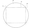
図1は、あるサイズの円形の単結晶半導体基板から、光電変換層を形成するために、所定の外形寸法の転置用半導体基板を切り出す態様を示す。単結晶半導体基板100の代表例は単結晶シリコンウエハであり、その他多結晶シリコンウエハも適用可能である。転置用半導体基板101は、各頂点が単結晶半導体基板100の円周に内接する正方形とすることで面積を最大にすることができるが、必ずしも正方形とする必要はない。例えば、光電変換装置を用いた太陽光発電モジュールを製造する場合、転置用半導体基板101は、モジュールのサイズに合わせて受光面積が最大になる形状とすれば良い。なお、シリコンウエハのサイズは直径300mm以上が好ましく、例えば、直径400mm若しくは直径450mmのシリコンウエハ(18インチシリコンウエハ)を適用することが好ましい。太陽光発電モジュールを製造する場合、複数のユニットセルを配列させた時に生じる隙間(非発電領域)の面積を縮小できるからである。
FIG. 1 shows a mode in which a semiconductor substrate for transfer having a predetermined outer dimension is cut out from a circular single crystal semiconductor substrate of a certain size in order to form a photoelectric conversion layer. A typical example of the single
図2は、円形の単結晶半導体基板から切り出した転置用半導体基板の態様を示す。図1で示すように、転置用半導体基板101を、頂点が単結晶半導体基板100の円周に内接する四辺形とし、切断線102と切断線103に沿って切り出した場合、図2に丸点線で示す角部104の頂点の角度が略90度となる。これは、転置用半導体基板101を単結晶半導体基板100の外周内側から切り出す場合にも同様である。
FIG. 2 shows an aspect of a semiconductor substrate for transfer cut out from a circular single crystal semiconductor substrate. As shown in FIG. 1, when the
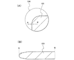
この場合、角部104が鋭端にならないように曲面加工することが好ましい。図3(A)、(B)は、転置用半導体基板の構成を示す。図3(A)は角部104の拡大図であり、このように曲面加工することで転置用半導体基板101の破損を防止することができる。また、図3(B)に示すように、転置用半導体基板101の周辺端部の稜角を削る面取加工を施して、断面形状を曲面形状又は多段角形状にすることが好ましい。これにより、基板の破損が防止されシリコン資源の無駄使いを減らすことができる。なお、切り出した後の端材は、溶融して再生することができる。
In this case, it is preferable to process the curved surface so that the
(単結晶半導体基板の加工2)
図4は、あるサイズの円形の単結晶半導体基板から、光電変換層を形成するために、所定の外形寸法の転置用半導体基板を切り出す態様として、図1とは異なるものを示す。単結晶半導体基板100の代表例は単結晶シリコンウエハであり、その他多結晶シリコンウエハも適用可能である。転置用半導体基板101は、各頂点が単結晶半導体基板100の円周に内接する正方形とすることで面積を最大にすることができるが、必ずしも正方形とする必要はないのは図1の場合と同様である。
(Processing of single crystal semiconductor substrate 2)
FIG. 4 shows a mode different from that in FIG. 1 as a mode of cutting out a semiconductor substrate for transfer having a predetermined outer dimension in order to form a photoelectric conversion layer from a circular single crystal semiconductor substrate of a certain size. A typical example of the single
図4で示すように、転置用半導体基板101を、円周に内接する矩形領域126よりも対辺の間隔が長くなるように切り出す。すなわち、切断線102と切断線103に沿って切断することにより、矩形の転置用半導体基板101の頂点が90度とならないように切り出すことができる。このように加工することで、図5で示すように、転置用半導体基板101において、表示パネルの製造に必要な面積を確保しつつ、角部が90度や鋭角とならない基板を作製することができる。転置用半導体基板101の角部が直角とならないことで、基板をハンドリングする際に破損することを防止できる。また、図3(B)で説明したように、転置用半導体基板101の周辺端部の稜角を削る面取加工を施して、断面形状を曲面形状又は多段角形状にすることが好ましい。これにより、基板の破損が防止されシリコン資源の無駄使いを減らすことができる。なお、切り出した後の端材は、溶融して再生することができる。
As shown in FIG. 4, the
(単結晶半導体層の配列)
図6は、転置用半導体基板101を支持基板105に貼り合わせるときの配置について、その一例を示している。
(Arrangement of single crystal semiconductor layers)
FIG. 6 shows an example of the arrangement when the
支持基板105は、ガラス基板、セラミックス基板などの耐熱性絶縁基板を用いることが好ましい。例えば、支持基板105としてガラス基板を用いる場合には、アルミノシリケートガラス、アルミノホウケイ酸ガラス、バリウムホウケイ酸ガラスのような電子工業用に使われる各種ガラスを用いる。ガラス基板としては、液晶パネルなどの用途に適用されるガラス基板を転用することができる。支持基板105は、一辺が500mm以上の四辺形のガラス基板を用いることができる。例えば、第3.5世代(600mm×720mm、又は620mm×750mm)、第4世代(680mm×880mm、又は730mm×920mm)のガラス基板を用いる。さらに、第6世代(1500mm×1850mm)、第7世代(1870mm×2200mm)、第8世代(2200mm×2400mm)といわれる大面積のマザーガラス基板を用いることも可能である。
The
大面積のガラス基板を支持基板105として用いることで、光電変換装置を用いた太陽光発電モジュールの大面積化が可能となり、生産性を向上させることができる。例えば、600mm×720mmのガラス基板を支持基板105とした場合には、直径450mmのシリコンウエハを使うことにより、280mm×350mmの転置用半導体基板101を4枚貼り合わせることができる。円形のシリコンウエハから前記した寸法の矩形の転置用半導体基板101を切り出すことにより、シリコンウエハの端材は残るが、矩形のガラス基板に密に転置用半導体基板101を配置させることが可能となる。また、730mm×920mmのガラス基板を用いた支持基板105の場合には、335mm×300mmの転置用半導体基板101を6枚貼り合わせることができる。
By using a large-area glass substrate as the
転置用半導体基板101には表面から10μm未満の領域、すなわち50nm以上10000nm未満、好ましくは100nmから5000nmの深さに損傷層が形成されている。この損傷層を境界として転置用半導体基板101から単結晶半導体層を分離して、支持基板105上に単結晶半導体層を形成する。転置用半導体基板101をから剥離した単結晶半導体層を用いて光電変換装置を製造する工程の詳細は、以下に示す実施形態によって明らかにされる。
A damage layer is formed on the
(実施形態1)
本形態では、単結晶半導体基板から薄い単結晶半導体層を分離して、絶縁表面を有する基板若しくは絶縁性の基板上に単結晶半導体層を転置することによって、太陽電池を用いた光電変換装置を製造する方法について図面を参照して説明する。
(Embodiment 1)
In this embodiment, a thin single crystal semiconductor layer is separated from a single crystal semiconductor substrate, and the single crystal semiconductor layer is transferred over a substrate having an insulating surface or an insulating substrate, whereby a photoelectric conversion device using a solar cell is obtained. A manufacturing method will be described with reference to the drawings.
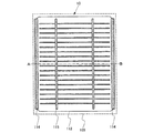
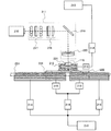
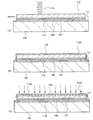
図7は本形態に係る光電変換装置10の平面図を示す。この光電変換装置10は、支持基板105上に貼り付けられた単結晶半導体層112に光が入射することで発電をする。単結晶半導体層112には、内蔵電界を形成するための不純物半導体層が形成されている。単結晶半導体層112としては、代表的には単結晶シリコンが適用される。また、単結晶半導体層112に代えて多結晶半導体層を適用することができる。この場合、多結晶シリコンが適用される。
FIG. 7 is a plan view of the
図7の例では、単結晶半導体層112の表面側に、網状の第2電極115が設けられ、裏面側に第1電極(平面図では表示されない)が設けられている。補助電極114は裏面側に設けられる第1電極と接続する電極である。本形態の光電変換装置10は、絶縁表面を有する支持基板105に単結晶半導体層112が接着される構成なので、正極とそれに対する負極の電極は、支持基板105の同じ面側に設けられる構成が主として採用される。
In the example of FIG. 7, a net-like
次に、図7のA−B切断線に対応する断面図を参照しながらこの光電変換装置10の製造工程について説明する。
Next, a manufacturing process of the
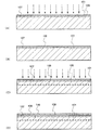
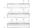
図8(A)に示す転置用半導体基板101は円形の単結晶半導体基板より略四辺形に切り出されたものである。転置用半導体基板101は、代表的には単結晶シリコンであって、表面が鏡面研磨されたものが好ましい。保護膜106は酸化シリコン又は窒化シリコンで形成することが好ましく、化学気相成長法により形成する。転置用半導体基板101に第1不純物半導体層を形成する際、表面にイオンが照射されて平坦性が損なわれてしまうため、保護膜106を設けることが好ましい。保護膜106は50nmから200nmの厚さで設けることが好ましい。
A
そして、転置用半導体基板101に一導電型の第1不純物半導体層107を形成する。例えば、一導電型を付与する不純物として硼素を添加して、第1不純物半導体層107としてp型の半導体層を形成する。第1不純物半導体層107は、本形態の光電変換装置において、光入射側と反対側の面に配置され、裏面電界(BSF:Back Surface Field)を形成する。硼素の添加は、B2H6、BF3をソースガスとして、生成されたイオンを質量分離しないで電界で加速して、生成されるイオン流を基板に照射するイオンドーピング装置を用いて行う。保護膜106を通してイオンを第1不純物半導体層107に添加することにより、イオンの照射による表面の損傷を防止することができる。
Then, a first
図8(B)は、保護膜106を除去して、第1不純物半導体層107上に第1電極108を形成している。第1電極108は耐熱性金属で形成することが好ましい。耐熱性金属としては、チタン、モリブデン、タングステン、クロムなどの金属材料が適用される。また、これらの金属材料の窒化物を第1不純物半導体層107に接して形成して、第1電極108を金属材料の窒化物で形成した層と耐熱性金属で形成した層との二層構造としても良い。金属材料の窒化物で形成した層を設けることで、第1電極108と第1不純物半導体層107との密着性を向上させることができる。第1電極108は真空蒸着法又はスパッタリング法で形成する。
In FIG. 8B, the
図8(C)は、第1電極108が形成された面から、水素イオンを含むイオンビームを転置用半導体基板101に照射して、損傷層109を形成する段階を示している。水素イオン、好ましくはH3 +に代表されるような、質量が水素分子よりも重いクラスターイオンを打ち込んで、表面から一定の深さの領域に損傷層109を形成する。損傷層109の深さは、イオンの加速エネルギーによって制御される。損傷層109の深さにより転置用半導体基板101から分離される単結晶半導体層の厚さが決まるので、クラスターイオンを加速する電界強度はそのことを考慮して決められる。損傷層109は、転置用半導体基板101の表面から10μm未満の深さ、すなわち50nm以上10000nm未満、好ましくは100nmから5000nmの深さに形成することが好ましい。また、第1電極108を通してクラスターイオンを転置用半導体基板101に打ち込むことで、イオンの照射により表面が損傷を受けてしまうことを防止することができる。また、第1不純物半導体層107を通して水素のクラスターイオンを打ち込んで損傷層109を形成することにより、第1不純物半導体層107の水素化を兼ねることができる。
FIG. 8C shows a stage in which the damaged
水素イオンであってH3 +に代表されるようなクラスターイオンは、水素プラズマを生成する。水素プラズマ中に生成されるイオンを質量分離せず、そのまま電界で加速することにより転置用半導体基板101に照射するイオンドーピング装置を用いて、損傷層109を形成することができる。イオンドーピング装置を用いることにより、面積の大きい転置用半導体基板101であっても容易に損傷層109を形成することができる。
Cluster ions such as H 3 + , which are hydrogen ions, generate hydrogen plasma. The damaged
図13は、イオン源200において生成された複数のイオンを、質量分離しないで転置用半導体基板101に照射するイオンドーピング装置の構成を説明する概略図である。イオン源200にはガス供給部204から水素等の所定のガスが供給される。イオン源200にはフィラメント201が備えられている。フィラメント電源202はフィラメント201へアーク放電電圧を印加し、フィラメント201に流れる電流を調節する。ガス供給部204から供給されたガスは、排気系209により排気される。
FIG. 13 is a schematic diagram illustrating a configuration of an ion doping apparatus that irradiates a
イオン源200で生成されたイオンは、引出し電極系205によって引き出され、イオンビーム117を形成する。イオンビーム117は載置台206に置かれた転置用半導体基板101に照射される。イオンビーム117に含まれるイオンの割合は載置台206の近傍に設けられた質量分析管207によって計量される。質量分析管207によって計数されたイオン密度は質量分析計208で信号変換され、その結果を電源制御部203にフィードバックさせるようにしても良い。電源制御部203はイオン密度の計数結果に従って、フィラメント電源202を制御することができる。
Ions generated by the
図13で示すように、ガス供給部204から供給された水素等のガスは、イオンドーピング装置のチャンバー内を流れ、排気系209によって排出される構成となっている。
As shown in FIG. 13, a gas such as hydrogen supplied from the
このことは、質量分析管207を用いて載置台206に流れ込んでくるイオンビーム117の質量分析結果を見れば明らかであり、水素イオンであるH+、H2 +、H3 +の総量に対してH3 +の割合は70%以上となっている。それにより、多量に生成されたクラスターイオンであるH3 +を含むイオンビーム117を転置用半導体基板101に照射することで、H+、H2 +を照射するよりも水素の添加効率が向上し、ドーズ量が少なくても水素を転置用半導体基板101に高濃度に含ませることができるという有意な効果を奏する。
This is apparent from the mass analysis result of the
このようにH3 +の割合を高めておくことで、損傷層109には1×10²⁰atoms/cm3以上の水素を含ませることが可能である。転置用半導体基板101に形成される損傷層109は結晶構造が失われ微小な空洞が形成され、多孔質構造となっている。そのため、比較的低温(600℃以下)の加熱処理によって損傷層109に形成された微小な空洞の体積変化が起こり、損傷層109に沿って分離した単結晶半導体層を得ることができる。
Thus, by increasing the ratio of H 3 + , the damaged
なお、略四辺形で形成される転置用半導体基板101の一辺の長さよりも長い線状イオンビームを、転置用半導体基板101の表面に走査して照射して、転置用半導体基板101にクラスターイオンを打ち込むことによって、深さが均一な損傷層109を形成することができる。
Note that a surface of the
図8(D)は、第1電極108上に接着層110を形成する段階を示す。接着層110は、酸化シリコン膜、酸化窒化シリコン膜、窒化酸化シリコン膜、窒化シリコン膜などの絶縁膜で形成する。接着層110は絶縁性の被膜を形成するものであれば、材料は限定されない。また、接着層110は平滑であり親水性の表面を有する膜で形成すれば良い。接着層110の平滑性でいえば、平均面粗さ(Ra)が1nm以下、好ましくは0.5nm以下であることが好ましい。なお、ここでいう平均面粗さとは、JIS B0601で定義されている「中心線平均粗さ」を面に対して適用できるよう三次元に拡張したものである。
FIG. 8D shows a step of forming the
平滑であり親水性の表面を形成する絶縁膜としては、水素を含有する酸化シリコン膜、水素を含有する窒化シリコン膜、酸素と水素を含有する窒化シリコン膜、酸化窒化シリコン膜、窒化酸化シリコン膜等を適用することができる。 As an insulating film that forms a smooth and hydrophilic surface, a silicon oxide film containing hydrogen, a silicon nitride film containing hydrogen, a silicon nitride film containing oxygen and hydrogen, a silicon oxynitride film, and a silicon nitride oxide film Etc. can be applied.
なお、酸化窒化シリコン膜とは、その組成として、窒素よりも酸素の含有量が多いものであって、ラザフォード後方散乱法(RBS:Rutherford Backscattering Spectrometry)及び水素前方散乱法(HFS:Hydrogen Forward Scattering)を用いて測定した場合に、濃度範囲として酸素が50〜70原子%、窒素が0.5〜15原子%、シリコンが25〜35原子%、水素が0.1〜10原子%の範囲で含まれるものをいう。また、窒化酸化シリコン膜とは、その組成として、酸素よりも窒素の含有量が多いものであって、RBS及びHFSを用いて測定した場合に、濃度範囲として酸素が5〜30原子%、窒素が20〜55原子%、シリコンが25〜35原子%、水素が10〜30原子%の範囲で含まれるものをいう。ただし、酸化窒化シリコンまたは窒化酸化シリコンを構成する原子の合計を100原子%としたとき、窒素、酸素、シリコン及び水素の含有比率が上記の範囲内に含まれるものとする。 Note that the silicon oxynitride film has a composition that contains more oxygen than nitrogen, and includes Rutherford Backscattering Spectroscopy (RBS) and Hydrogen Forward Scattering (HFS). The concentration ranges from 50 to 70 atomic%, nitrogen from 0.5 to 15 atomic%, silicon from 25 to 35 atomic%, and hydrogen from 0.1 to 10 atomic%. Means what In addition, the silicon nitride oxide film has a composition containing more nitrogen than oxygen. When measured using RBS and HFS, the concentration range of oxygen is 5 to 30 atomic%, nitrogen. Is contained in the range of 20 to 55 atomic%, silicon of 25 to 35 atomic%, and hydrogen of 10 to 30 atomic%. However, when the total number of atoms constituting silicon oxynitride or silicon nitride oxide is 100 atomic%, the content ratio of nitrogen, oxygen, silicon, and hydrogen is included in the above range.
水素を含有する酸化シリコン膜としては、例えば有機シランを用いて化学気相成長法により作製される酸化シリコン膜を用いることが好ましい。接着層110として、例えば有機シランを用いて形成された酸化シリコン膜を用いることによって、支持基板と転置した単結晶半導体層との接合を強固にすることができるためである。有機シランとしては、テトラエトキシシラン(TEOS:化学式Si(OC2H5)4)、テトラメチルシラン(TMS:化学式Si(CH3)4)、テトラメチルシクロテトラシロキサン(TMCTS)、オクタメチルシクロテトラシロキサン(OMCTS)、ヘキサメチルジシラザン(HMDS)、トリエトキシシラン(SiH(OC2H5)3)、トリスジメチルアミノシラン(SiH(N(CH3)2)3)等のシリコン含有化合物を用いることができる。
As the silicon oxide film containing hydrogen, it is preferable to use, for example, a silicon oxide film manufactured by chemical vapor deposition using organosilane. This is because, for example, by using a silicon oxide film formed using organosilane as the
水素を含有する窒化シリコン膜は、シランガスとアンモニアガスを用いてプラズマCVD法により作製することができる。前記ガスに水素が加えられていても良い。酸素と水素を含有する窒化シリコン膜は、シランガスとアンモニアガスと亜酸化窒素ガスを用いてプラズマCVD法で作製することができる。いずれにしても、プラズマCVD法、減圧CVD法、常圧CVD法等の化学気相成長法により、シランガス等を原料ガスとして用いて作製される酸化シリコン、酸化窒化シリコン、窒化酸化シリコンなどの絶縁膜であって水素が含まれるものであれば適用することができる。接着層110は、単結晶半導体基板に形成した損傷層109から水素が脱離しない温度である350℃以下で形成することが推奨される。
A silicon nitride film containing hydrogen can be manufactured by a plasma CVD method using silane gas and ammonia gas. Hydrogen may be added to the gas. A silicon nitride film containing oxygen and hydrogen can be manufactured by a plasma CVD method using silane gas, ammonia gas, and nitrous oxide gas. In any case, insulation of silicon oxide, silicon oxynitride, silicon nitride oxide, etc. produced using a silane gas or the like as a source gas by a chemical vapor deposition method such as a plasma CVD method, a low pressure CVD method, or an atmospheric pressure CVD method. Any film can be used as long as it contains hydrogen. The
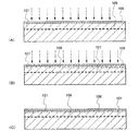
図9(A)は支持基板105と転置用半導体基板101とを接着する段階を示す。この接着は、平滑であり親水性の表面を有する接着層110が支持基板105に密着することにより成される。この接合には、水素結合やファン・デル・ワールス力が作用している。接着層110の表面が親水性を有すると、水酸基や水分子が接着剤として働き、後の加熱処理によって水分子が拡散し、残留成分によってシラノール基(Si−OH)が形成され、シラノール基が作用して水素結合により接合を形成する。さらにこの水素結合による接合は、水素が抜けることでシロキサン結合(O−Si−O)が形成されて共有結合になり、転置用半導体基板101と支持基板105の接合が強固なものとなる。なお、支持基板105の接着面にも、バリア層111として窒化シリコン膜、窒化酸化シリコン膜などを形成しておいても良い。バリア層111を形成することで、支持基板105からの不純物汚染を防止することができる。
FIG. 9A shows a stage in which the supporting
また、支持基板105と接着層110との接着を良好に行うために、接着面を活性化しておくことは好ましい。例えば、接着面の一方又は双方に原子ビーム若しくはイオンビームを照射する。原子ビーム若しくはイオンビームを利用する場合には、アルゴン等の不活性ガス中性原子ビーム若しくは不活性ガスイオンビームを用いることができる。その他に、プラズマ照射若しくはラジカル処理を行うことで接着面を活性化することもできる。このような表面処理により、後の加熱処理の温度が400℃以下であっても異種材料間の接合を形成することが容易となる。
Further, it is preferable to activate the bonding surface in order to achieve good bonding between the
図9(B)は、加熱処理により損傷層109を境界として転置用半導体基板101の表層部を分離して支持基板105に転置する段階を示す。加熱処理は接着層110の成膜温度以上、支持基板105の耐熱温度以下で行うことが好ましい。例えば400℃から600℃の加熱処理を行うことにより、損傷層109に形成された微小な空洞の堆積変化が起こり、その領域に沿って分離する。接着層110は支持基板105と接着しているので、支持基板105には単結晶半導体層112と第1電極108が残存する。このとき、単結晶半導体層112の厚さは、損傷層の深さにほぼ対応し、50nm以上10000nm未満、好ましくは100nmから5000nmの厚さに形成される。
FIG. 9B shows a stage in which the surface layer portion of the
以上の工程により、支持基板105上に接着層110により固定された単結晶半導体層112を設けることができる。単結晶半導体層112の分離された面は、平均面粗さ(Ra)が7nm〜10nm、最大高低差(P−V)が300nm〜400nmの値を有している。なお、ここでいう最大高低差とは、山頂と谷底の高さの差を示す。また、ここでいう山頂と谷底とはJIS B0601で定義されている「山頂」「谷底」を三次元に拡張したものであり、山頂とは指定面の山において最も標高の高いところ、谷底とは指定面の谷において最も標高の低いところと表現される。また、損傷層109を形成するために打ち込まれたイオンによって、単結晶半導体層112に結晶欠陥が形成されている。
Through the above steps, the single
なお図10で示すように、単結晶半導体層112は、支持基板105上に複数個を一度に接着することができる。例えば、600mm×720mmの支持基板105に、280mm×350mmの転置用半導体基板101を4枚貼り合わせることができる。
Note that a plurality of single crystal semiconductor layers 112 can be bonded to the supporting
図11(A)は、単結晶半導体層112に第1不純物半導体層107とは逆の導電型を付与する不純物を添加して、第2不純物半導体層113を形成する。例えば、リン又は砒素を添加して第2不純物半導体層113としてn型の半導体層を形成する。
In FIG. 11A, an impurity imparting a conductivity type opposite to that of the first
なお、単結晶半導体層112の表面は損傷層109に最も近い領域、又は損傷層109の一部を含む領域であるので、後のレーザ処理の前に表層をエッチングにより除去しておくことが好ましい。エッチングとしてドライエッチング又はウエットエッチングを行えば良い。
Note that since the surface of the single
図11(B)は、単結晶半導体層112に残留する結晶欠陥の修復をするために、レーザ処理をする段階を示している。レーザビーム118を単結晶半導体層112に照射することで、単結晶半導体層112の少なくとも表面側(単結晶半導体層112の表層)は溶融し、後の冷却過程で固相状態の下層部を種結晶として再単結晶化する。その過程で単結晶半導体層112の表面は平坦化されて単結晶半導体層112aを得ることができる。また、第2不純物半導体層113のレーザ処理によって、不純物元素が表面側に高濃度に分布した第2不純物半導体層113aを得ることができる。このレーザ処理のとき、少なくともレーザビームの照射領域は250℃から600℃の温度に加熱されていることが好ましい。照射領域を加熱しておくことで、レーザビームの照射による溶融時間を長くすることができ、欠陥の修復をより効果的に行うことができる。レーザビーム118の照射により単結晶半導体層112の表面側は溶融するものの、支持基板105は殆ど加熱されないので、ガラス基板のような耐熱性の低い基板を支持基板105として用いることが可能になる。また、第1電極108は耐熱性金属で形成されているので、上記温度で加熱されても単結晶半導体層112に悪影響を及ぼすことがない。第1電極108と第1不純物半導体層107の界面ではシリサイドが形成され、より電流が流れ易くなる。このレーザ処理は第2不純物半導体層113の活性化を兼ねている。
FIG. 11B shows a stage in which laser treatment is performed in order to repair crystal defects remaining in the single
このレーザ処理を行うためのレーザ処理装置の一例を、図14を参照して説明する。レーザ処理装置は、レーザ発振器210、レーザ光を集光及び伸長して断面形状が細い線状のレーザビームを形成する光学系211、レーザビームの照射領域の雰囲気を制御するガス噴射筒212、ガス噴射筒212に雰囲気制御ガスを供給するガス供給部213、流量制御部214、ガス加熱部215、支持基板105を浮遊させ搬送する基板ステージ222、基板の両端を支持して搬送するガイドレール223、基板ステージ222に浮遊用のガスを供給するガス供給部216を備えている。
An example of a laser processing apparatus for performing this laser processing will be described with reference to FIG. The laser processing apparatus includes a
レーザ発振器210は、その発振波長が、紫外光域乃至可視光域にあるものが選択される。レーザ発振器210は、パルス発振型のArF、KrF又はXeClエキシマレーザ、或いはNd:YAGレーザ、YLFレーザなどの固体レーザで、繰り返し周波数1MHz以下、パルス幅10n秒以上500n秒以下のものが好ましい。例えば、繰り返し周波数10Hz〜300Hz、パルス幅25n秒、波長308nmのXeClエキシマレーザを用いる。
As the
光学系211はレーザ光を集光及び伸張して、被照射面に断面形状が線状のレーザビームを形成する。線状レーザビームを形成する光学系211は、シリンドリカルレンズアレイ217、シリンドリカルレンズ218、ミラー219、ダブレットシリンドリカルレンズ220により構成される。レンズの大きさにもよるが、長手方向は100mm〜700mm、短手方向は100〜500μm程度の線状レーザビームを形成することが可能である。
The
線状に集光及び伸長されたレーザビームはガス噴射筒212の光導入窓221を通して支持基板105に照射される。ガス噴射筒212は支持基板105と近接して配置されている。ガス噴射筒212にはガス供給部213から窒素ガスが供給されている。窒素ガスはガス噴射筒212の支持基板105に面した開口部から噴射する。ガス噴射筒212の開口部は、光導入窓221から入射したレーザビームが支持基板105に照射されるように、線状のレーザビーム118の光軸に合わせて配置されている。ガス噴射筒212の開口部から噴射する窒素ガスにより、レーザビームの照射領域は窒素雰囲気となる。
The laser beam condensed and extended linearly is applied to the
ガス噴射筒212に供給する窒素ガスをガス加熱部215で250℃から600℃に加熱することにより、加熱された窒素ガスで支持基板105の、レーザビーム照射面の温度を制御することができる。照射領域を加熱しておくことで、上記のようにレーザビームの照射による溶融時間を制御することができる。
By heating the nitrogen gas supplied to the
基板ステージ222には、ガス供給部216から空気又は窒素が流量制御部214を通して供給される。ガス供給部216から供給される気体は、基板ステージ222の主面から、支持基板105の下面を吹き付けるように噴出させて、支持基板105を浮遊させる。支持基板105は両端がガイドレール223上を動くスライダ224に載せられて搬送されるが、基板ステージ222側からガスが吹き付けられることにより、湾曲せずに浮遊した状態で搬送することができる。本形態のレーザ処理装置では、支持基板105の上面にガス噴射筒212から窒素ガスを噴出させ、その下面にもガスを吹き付けることにより、支持基板105の撓みを防ぐことができる。このような基板ステージ222の構成は、一辺が500mmを超え、厚さが1mm以下のガラス基板を処理する場合に有効である。例えば、600mm×720mmないし730mm×920mmで厚さが0.7mm以下のガラス基板を処理することができる。
Air or nitrogen is supplied to the
基板ステージ222は、レーザ照射部近傍と、それ以外の領域に区画されていても良い。基板ステージ222のレーザ照射部近傍では、ガス加熱部215により加熱された窒素ガスを吹き付けるようにしても良い。それにより、支持基板105を加熱することができる。
The
図15はこのようなレーザ処理装置によって、支持基板105上の単結晶半導体層112に対しレーザ処理をする態様を示している。複数の単結晶半導体層112が支持基板105上に接着されており、線状に集光および伸長されたレーザビーム118は、支持基板105が移動することにより全面に照射することができる。
FIG. 15 shows a mode in which laser processing is performed on the single
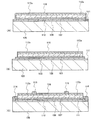
図11(C)は、単結晶半導体層112aの端部をエッチングして第1電極108を露出させる段階を示している。エッチングは単結晶半導体層112aにマスクを形成し、NF3、SF6などのガスを用いてドライエッチングを行えば良い。
FIG. 11C illustrates a step of exposing the
図12(A)は、第1電極108に接する補助電極114と、第2不純物半導体層113a上の第2電極115を形成する段階を示している。補助電極114は図11(C)でエッチングにより露出した第1電極108に接触するように形成する。第2電極115は、図7の平面図で示すように櫛型又は格子状の電極である。補助電極114及び第2電極115は、アルミニウム、銀、鉛錫(半田)などで形成すれば良い。例えば、銀ペーストを用いてスクリーン印刷法で形成する。
FIG. 12A shows a step of forming the
その後、図12(B)で示すように、パッシベーション膜を兼ねた反射防止膜116を形成する。反射防止膜116は、窒化シリコン膜で形成することが好ましく、窒化シリコン膜と窒化酸化シリコン膜との積層で形成しても良い。
After that, as shown in FIG. 12B, an
このようにして図7で示す光電変換装置10を製造することができる。本工程によれば、異種材料間の接合技術と、レーザ処理技術を用いることにより、700℃以下(好適には500℃以下)のプロセス温度で10μm以下の単結晶半導体層を有する光電変換装置を製造することができる。すなわち、耐熱温度が700℃以下の大面積ガラス基板に、単結晶半導体層を設けた光電変換装置を製造することができる。単結晶半導体層は単結晶半導体基板の表層部を分離することにより得られるが、単結晶半導体層の表層部を分離した後の単結晶半導体基板は繰り返し利用することができるので資源を有効に利用することができる。
In this way, the
(実施形態2)
本形態は、実施形態1と異なる製造工程を図16(A)〜(C)に示す。図16(A)に示すように、転置用半導体基板101に保護膜106を形成し、保護膜106を通して一導電型を付与する不純物を添加して第1不純物半導体層107を形成した後、図16(B)に示すように、保護膜106をそのまま残して、水素のクラスターイオンを打ち込み損傷層109を形成する。その後、図16(C)に示すように、保護膜106を除去し、第1電極108を形成する。
(Embodiment 2)
In this embodiment, manufacturing steps different from those in Embodiment 1 are shown in FIGS. As shown in FIG. 16A, a
このような工程とすることで、保護膜106をイオンドーピングにおける損傷防止層として有効に利用することができる。すなわち、イオンの照射で損傷を受けた保護膜106を、第1電極108の形成前に除去することで、転置用半導体基板101の表面の損傷を防止することができる。また、第1不純物半導体層107を通して水素のクラスターイオンを打ち込んで損傷層109を形成することにより、第1不純物半導体層107の水素化を兼ねることができる。
By setting it as such a process, the
(実施形態3)
本形態は、実施形態1と異なる製造工程を図17(A)〜(C)に示す。図17(A)に示すように、転置用半導体基板101に第1電極108を形成し、図17(B)に示すように、第1電極108を通して一導電型を付与する不純物を添加して第1不純物半導体層107を形成する。そして、図17(C)に示すように、第1電極108と第1不純物半導体層107を通して水素のクラスターイオンを打ち込み損傷層109を形成する。
(Embodiment 3)
In this embodiment, manufacturing steps different from those in Embodiment 1 are shown in FIGS. As shown in FIG. 17A, the
本工程では、第1電極108を通して第1不純物半導体層107を形成することにより、第1不純物半導体層107の厚さを制御することが容易となる。また、第1電極108を形成した後に、損傷層109を形成することにより、第1電極108をイオンドーピングにおける損傷防止層として利用することができる。これにより、イオンドーピングのために保護膜を形成する工程を省略することができる。さらに、第1不純物半導体層107を通して水素のクラスターイオンを打ち込んで損傷層109を形成することにより、第1不純物半導体層107の水素化を兼ねることができる。
In this step, it is easy to control the thickness of the first
(実施形態4)
本形態は、実施形態1と異なる製造工程を図18(A)〜(C)に示す。図18(A)に示すように、転置用半導体基板101に第1電極108を形成し、図18(B)に示すように、第1電極108を通して水素のクラスターイオンを打ち込み損傷層109を形成する。そして、図18(C)に示すように、第1電極108を通して一導電型を付与する不純物を添加して第1不純物半導体層107を形成する。
(Embodiment 4)
In this embodiment, manufacturing steps different from those in Embodiment 1 are shown in FIGS. As shown in FIG. 18A, a
本工程では、第1電極108を通して第1不純物半導体層107を形成することにより、第1不純物半導体層107の厚さを制御することが容易となる。また、第1電極108を形成した後に、損傷層109を形成することにより、第1電極108をイオンドーピングにおける損傷防止層として利用することができる。これにより、イオンドーピングのために保護膜を形成する工程を省略することができる。さらに、損傷層109を形成した後に、第1不純物半導体層107を形成することにより、第1不純物半導体層107の不純物濃度を高濃度化することができ、浅い接合を形成することができる。これにより、裏面電界(BSF:Back Surface Field)効果により光生成キャリアの収集効率の高い光電変換装置を製造することができる。
In this step, it is easy to control the thickness of the first
(実施形態5)
本形態は、実施形態1と異なる製造工程を図19(A)〜(C)に示す。図19(A)に示すように、転置用半導体基板101に保護膜106を形成し、水素のクラスターイオンを打ち込み損傷層109を形成し、図19(B)に示すように、保護膜106をそのまま残して、一導電型を付与する不純物を添加して第1不純物半導体層107を形成する。そして、図19(C)に示すように、保護膜106を除去し、第1電極108を形成する。
(Embodiment 5)
In the present embodiment, manufacturing steps different from those in the first embodiment are shown in FIGS. As shown in FIG. 19A, a
このような工程とすることで、保護膜106をイオンドーピングにおける損傷防止層として有効に利用することができる。すなわち、イオンの照射で損傷を受けた保護膜106を、第1電極108の形成前に除去することで、転置用半導体基板101の表面の損傷を防止することができる。また、損傷層109を形成した後に、第1不純物半導体層107を形成することにより、第1不純物半導体層107の不純物濃度を高濃度化することができ、浅い接合を形成することができる。これにより、裏面電界(BSF:Back Surface Field)効果により光生成キャリアの収集効率の高い光電変換装置を製造することができる。
By setting it as such a process, the
(実施形態6)
本形態は、実施形態1と異なる製造工程を図20(A)〜(C)に示す。図20(A)に示すように、転置用半導体基板101に保護膜106を形成し、保護膜106を通して水素のクラスターイオンを打ち込み損傷層109を形成し、図20(B)に示すように、保護膜106を除去し、第1電極108を形成する。そして、図20(C)に示すように、第1電極108を通して一導電型を付与する不純物を添加して第1不純物半導体層107を形成する。
(Embodiment 6)
In this embodiment, manufacturing steps different from those in Embodiment 1 are shown in FIGS. As shown in FIG. 20A, a
保護膜106をイオンドーピングにおける損傷防止層として有効に利用することができる。すなわち、イオンの照射で損傷を受けた保護膜106を、第1電極108の形成前に除去することで、転置用半導体基板101の表面の損傷を防止することができる。また、損傷層109を形成した後に、第1不純物半導体層107を形成することにより、第1不純物半導体層107の不純物濃度を高濃度化することができ、浅い接合を形成することができる。これにより、裏面電界(BSF:Back Surface Field)効果により光生成キャリアの収集効率の高い光電変換装置を製造することができる。さらに、第1電極108を通して第1不純物半導体層107を形成することにより、第1不純物半導体層107の厚さを制御することが容易となる。
The
(実施形態7)
本形態は、実施形態1と異なる製造工程を図21(A)〜(C)に示す。支持基板105上に単結晶半導体層112を接着し、第2不純物半導体層113を形成し、レーザ処理を行った後(図11(B))、図21(A)に示すように反射防止膜116を形成する。その後、図21(B)で示すように、単結晶半導体層112aの端部をエッチングして第1電極108を露出させ、図21(C)で示すように第2電極115及び補助電極114を形成する。第2電極115は反射防止膜116上に形成されるが、絶縁破壊電圧を瞬間的に印加してバーンインコンタクトを形成することにより電極として機能させることができる。
(Embodiment 7)
In this embodiment, manufacturing steps different from those in Embodiment 1 are shown in FIGS. After the single
本形態は、実施形態2〜6と自由に組み合わせることができる。 This embodiment can be freely combined with Embodiments 2 to 6.
(実施形態8)
本形態では、実施形態1と異なる製造方法を図22(A)〜(C)、図23(A)、(B)に示す。支持基板105上に単結晶半導体層112を接着した後(図9(B))、図22(A)で示すように、単結晶半導体層112に残留する結晶欠陥の修復をするために、レーザ処理を行う。レーザビーム118を単結晶半導体層112に照射することで、単結晶半導体層112の少なくとも表面側は溶融し、後の冷却過程で固相状態の下層部を種結晶として再単結晶化する。その過程で単結晶半導体層112の表面は平坦化されて単結晶半導体層112bを得ることができる。このレーザ処理のとき、少なくともレーザビームの照射領域は、250℃から600℃の温度に加熱されていることが好ましい。照射領域を加熱しておくことで、レーザビームの照射による溶融時間を長くすることができ、欠陥の修復をより効果的に行うことができる。レーザビーム118の照射により単結晶半導体層112の表面側は溶融するものの、支持基板105は殆ど加熱されないので、ガラス基板のような耐熱性の低い基板を支持基板105として用いることが可能になる。また、第1電極108は耐熱性金属で形成されているので、上記温度で加熱されても単結晶半導体層112に悪影響を及ぼすことがない。第1電極108と第1不純物半導体層107の界面ではシリサイドが形成され、より電流が流れ易くなる。
(Embodiment 8)
In this embodiment, a manufacturing method different from that in Embodiment 1 is shown in FIGS. 22 (A) to (C), FIGS. 23 (A) and 23 (B). After the single
なお、単結晶半導体層112の表面は損傷層109に最も近い領域、又は損傷層109の一部を含む領域であるので、レーザ処理の前に表層をエッチングにより除去しておくことが好ましい。エッチングとしてドライエッチング又はウエットエッチングを行えば良い。
Note that since the surface of the single
レーザ処理には、一例として図14に示すレーザ処理装置を用いることができる。また、このようなレーザ処理装置によって、図15に示すように、支持基板105上の単結晶半導体層112のレーザ処理を行うことができる。
For example, a laser processing apparatus shown in FIG. 14 can be used for the laser processing. In addition, such a laser processing apparatus can perform laser processing on the single
その後、図22(B)で示すように、単結晶半導体層112bに第1不純物半導体層107とは逆の導電型を付与する不純物を添加して、第2不純物半導体層113bを形成する。例えば、リン又は砒素を添加して第2不純物半導体層113bとしてn型の半導体層を形成する。この場合、単結晶半導体層112bは、先の工程でレーザ処理により表面の結晶欠陥が修復され、平坦化されているので、第2不純物半導体層113bの不純物濃度と、添加深さを精密に制御することができる。すなわち、レーザビームを照射して、単結晶半導体層112の表面を処理し、その後不純物を添加して第2不純物半導体層113bを形成することにより、第2不純物半導体層113bに含まれる不純物の濃度を高濃度化することができ、浅い接合を形成することができる。それにより、光生成キャリアの収集効率の高い光電変換装置を得ることができる。また、第2不純物半導体層113bの形成前にレーザ処理を行うことにより、レーザビームの照射による溶融領域を単結晶半導体層112の内部深くまで広げることができ、再単結晶化による欠陥修復の効果をより高めることができる。
After that, as illustrated in FIG. 22B, an impurity imparting a conductivity type opposite to that of the first
図22(C)は、単結晶半導体層112bの端部をエッチングして第1電極108を露出させる段階を示している。エッチングは単結晶半導体層112bにマスクを形成し、NF3、SF6などのガスを用いてドライエッチングを行えば良い。
FIG. 22C shows a step of exposing the
図23(A)は、第1電極108に接する補助電極114と、第2不純物半導体層113b上の第2電極115を形成する段階を示している。補助電極114は図11(C)でエッチングにより露出した第1電極108に接触するように形成する。第2電極115は、図7の平面図で示すように櫛型又は格子状の電極である。補助電極114及び第2電極115は、アルミニウム、銀、鉛錫(半田)などで形成すれば良い。例えば、銀ペーストを用いてスクリーン印刷法で形成する。
FIG. 23A shows a stage in which the
その後、図23(B)で示すように、パッシベーション膜を兼ねた反射防止膜116を形成する。反射防止膜116は、窒化シリコン膜で形成することが好ましく、窒化シリコン膜と窒化酸化シリコン膜との積層膜で形成しても良い。
After that, as shown in FIG. 23B, an
このようにして図7で示す光電変換装置10を製造することができる。本工程によれば、異種材料間の接合技術と、レーザ処理技術を用いることにより、700℃以下(好適には500℃以下)のプロセス温度で10μm以下の単結晶半導体層を有する光電変換装置を製造することができる。すなわち、耐熱温度が700℃以下の大面積ガラス基板に、単結晶半導体層を設けた光電変換装置を製造することができる。単結晶半導体層は単結晶半導体基板の表層部を分離することにより得られるが、単結晶半導体層の表層部を分離した後の単結晶半導体基板は繰り返し利用することができるので資源を有効に利用することができる。
In this way, the
本形態は、実施形態2〜6と自由に組み合わせることができる。 This embodiment can be freely combined with Embodiments 2 to 6.
(実施形態9)
本形態は、実施形態1と異なる製造工程を図24(A)〜(C)、図25(A)、図25(B)に示す。支持基板105上に単結晶半導体層112を接着した後(図9(B))、図22(A)で説明したように、図24(A)で示すように、単結晶半導体層112に残留する結晶欠陥の修復をするためにレーザ処理を行う。
(Embodiment 9)
In this embodiment mode, manufacturing steps different from those in Embodiment Mode 1 are shown in FIGS. 24 (A) to (C), FIG. 25 (A), and FIG. After the single
その後、図22(B)で説明したように、図24(B)で示すように、単結晶半導体層112bに第1不純物半導体層107とは逆の導電型を付与する不純物を添加して、第2不純物半導体層113bを形成する。第2不純物半導体層113bの形成前にレーザ処理を行うことにより、レーザビームの照射による溶融領域を単結晶半導体層112の内部深くまで広げることができ、再単結晶化による欠陥修復の効果をより高めることができる。
After that, as described with reference to FIG. 22B, as shown in FIG. 24B, an impurity imparting a conductivity type opposite to that of the first
そして、図24(C)に示すように反射防止膜116を形成する。
Then, an
その後、図25(A)で示すように、単結晶半導体層112bの端部をエッチングして第1電極108を露出させ、図25(B)で示すように第2電極115及び補助電極114を形成する。第2電極115は反射防止膜116上に形成されるが、絶縁破壊電圧を瞬間的に印加してバーンインコンタクトを形成することにより電極として機能させることができる。
After that, as shown in FIG. 25A, the end portion of the single
本形態によれば、単結晶半導体層112bに第2不純物半導体層113bを形成した後にパッシベーション膜としても機能する反射防止膜116を形成することで、表面再結合速度を低くすることができ、光電変換装置の変換効率を高めることができる。
According to this embodiment, the surface recombination rate can be reduced by forming the
本形態は、実施形態2〜6と自由に組み合わせることができる。 This embodiment can be freely combined with Embodiments 2 to 6.
(実施形態10)
本形態は、実施形態1と異なる製造工程を図26(A)〜(C)に示す。支持基板105上に単結晶半導体層112を接着した後(図9(B))、図22(A)で説明したように、図26(A)で示すように、単結晶半導体層112に残留する結晶欠陥の修復をするために、レーザ処理を行う。レーザビーム118を単結晶半導体層112に照射することで、単結晶半導体層112の少なくとも表面側は溶融し、後の冷却過程で固相状態の下層部を種結晶として再単結晶化する。その過程で単結晶半導体層112の表面は平坦化されて単結晶半導体層112bを得ることができる。
(Embodiment 10)
In this embodiment, manufacturing steps different from those in Embodiment 1 are shown in FIGS. After the single
その後、図26(B)で示すように反射防止膜116を形成する。
Thereafter, an
そして、図26(C)で示すように、単結晶半導体層112bに第1不純物半導体層107とは逆の導電型を付与する不純物を添加して、第2不純物半導体層113bを形成する。本形態によれば、第2不純物半導体層113bの形成前にレーザ処理を行うことにより、レーザビームの照射による溶融領域を単結晶半導体層112の内部深くまで広げることができ、再単結晶化による欠陥修復の効果をより高めることができる。
Then, as illustrated in FIG. 26C, an impurity imparting a conductivity type opposite to that of the first
その後、図25(A)のように単結晶半導体層112bの端部をエッチングして第1電極108を露出させ、図25(B)で示すように第2電極115及び補助電極114を形成する。第2電極115は反射防止膜116上に形成されるが、絶縁破壊電圧を瞬間的に印加してバーンインコンタクトを形成することにより電極として機能させることができる。
After that, the end portion of the single
本形態は、実施形態2〜6と自由に組み合わせることができる。 This embodiment can be freely combined with Embodiments 2 to 6.
(実施形態11)
本形態は、実施形態1と異なる製造工程を図27(A)〜(C)に示す。支持基板105上に単結晶半導体層112を接着し(図9(B))、単結晶半導体層112に残留する結晶欠陥の修復をするために、レーザ処理を行った後(図22(A))、図27(A)で示すように、単結晶半導体層112bに絶縁層119を形成する。
(Embodiment 11)
In this embodiment, manufacturing steps different from those in Embodiment 1 are shown in FIGS. After the single
そして、図27(B)で示すように、絶縁層119に開口部を形成して単結晶半導体層112bを露出させた後、第1不純物半導体層107とは逆の導電型を付与する不純物を添加して、その開口部に第2不純物半導体層113bを形成する。第2不純物半導体層113bの形成前にレーザ処理を行うことにより、レーザビーム118の照射による溶融領域を単結晶半導体層112の内部深くまで広げることができ、再単結晶化による欠陥修復の効果をより高めることができる。
27B, an opening is formed in the insulating
その後、図27(C)で示すように、絶縁層119と単結晶半導体層112bを貫通し第1電極108に達する開口部を形成し、補助電極114及び第2電極115を形成する。さらに反射防止膜116を形成する。本形態のように、単結晶半導体層112bの内側に開口部を形成して第1電極108と導通する補助電極114を形成することにより、光電変換装置の小型化を図ることができる。
After that, as illustrated in FIG. 27C, an opening that penetrates the insulating
本形態は、実施形態2〜6と自由に組み合わせることができる。 This embodiment can be freely combined with Embodiments 2 to 6.
本実施例では、本発明により製造される光電変換装置を用いた太陽光発電モジュールと、太陽光発電モジュールを用いた太陽光発電システムの一例について説明する。 In this embodiment, an example of a solar power generation module using the photoelectric conversion device manufactured according to the present invention and a solar power generation system using the solar power generation module will be described.
図28(A)、(B)に、太陽光発電モジュールの構成を示す。図28(A)の太陽光発電モジュール12は、支持基板105に接着された単結晶半導体層112により光電変換装置10が構成されている。単結晶半導体層112には光電変換機能を発現させる第1不純物半導体層、第2不純物半導体層などが形成されている。
28A and 28B show the configuration of a photovoltaic power generation module. In the solar
補助電極114は単結晶半導体層112の裏面側に形成されている第1電極と接続する電極であり、第2電極115は櫛形又は格子状の電極である。補助電極114と第2電極115は支持基板105の一面に形成され、支持基板105の端部領域でコネクタ用の第1裏面電極120と第2裏面電極121とそれぞれ接続する。図28(B)は、図28(A)のC−D切断線に対応する断面図であり、支持基板105の貫通口を通して補助電極114と第2電極115が第1裏面電極120と第2裏面電極121にそれぞれ接続している。
The
このように、支持基板105に単結晶半導体層112を接着して光電変換装置10を形成することにより、太陽光発電モジュールの薄型化を図ることができる。
In this manner, by forming the
図29に、太陽光発電モジュール12を用いた太陽光発電システムの一例を示す。一又は複数の太陽光発電モジュール12の出力電力は、充電制御回路122により蓄電池123を充電する。蓄電池123の充電量が多い場合には、負荷124に直接出力される場合もある。
FIG. 29 shows an example of a solar power generation system using the solar
蓄電池123として電気二重層キャパシタを用いると、充電に化学反応を必要とせず、急速に充電することができる。また、化学反応を利用する鉛蓄電池などに比べ、寿命を約8倍、充放電効率を1.5倍に高めることができる。負荷124としては、蛍光灯、発光ダイオード、エレクトロルミネッセンスパネルなどの照明、小型の電子機器など、さまざまな用途に応用することができる。
When an electric double layer capacitor is used as the
10 光電変換装置
12 太陽光発電モジュール
100 単結晶半導体基板
101 転置用半導体基板
102 切断線
103 切断線
104 角部
105 支持基板
106 保護膜
107 第1不純物半導体層
108 第1電極
109 損傷層
110 接着層
111 バリア層
112 単結晶半導体層
112a 単結晶半導体層
112b 単結晶半導体層
113 第2不純物半導体層
113a 第2不純物半導体層
113b 第2不純物半導体層
114 補助電極
115 第2電極
116 反射防止膜
117 イオンビーム
118 レーザビーム
119 絶縁層
120 第1裏面電極
121 第2裏面電極
122 充電制御回路
123 蓄電池
124 負荷
126 矩形領域
200 イオン源
201 フィラメント
202 フィラメント電源
203 電源制御部
204 ガス供給部
205 引出し電極系
206 載置台
207 質量分析管
208 質量分析計
209 排気系
210 レーザ発振器
211 光学系
212 ガス噴射筒
213 ガス供給部
214 流量制御部
215 ガス加熱部
216 ガス供給部
217 シリンドリカルレンズアレイ
218 シリンドリカルレンズ
219 ミラー
220 ダブレットシリンドリカルレンズ
221 光導入窓
222 基板ステージ
223 ガイドレール
224 スライダ
DESCRIPTION OF
Claims (11)
前記単結晶半導体基板の前記イオンビームの照射面側に少なくとも一導電型の第1不純物半導体層と、前記第1不純物半導体層に接する第1電極と、前記第1電極上に接合層と、を形成し、
絶縁表面を有する支持基板の一面に、複数の前記単結晶半導体基板を、前記接合層を密接させて配列し、
加熱処理を行うことにより、前記支持基板上に単結晶半導体層を残存させたまま、前記損傷層を境界として前記単結晶半導体基板の一部を分離し、
前記単結晶半導体層の、前記単結晶半導体基板の一部の分離により露出した面側に、前記一導電型とは逆の導電型の第2不純物半導体層を形成し、
前記第2不純物半導体層側から前記単結晶半導体層にレーザビームを照射して、前記単結晶半導体層の表面を平坦化することを特徴とする光電変換装置の製造方法。 A single crystal semiconductor substrate is irradiated with an ion beam containing 70% or more of hydrogen cluster ions to form a damaged layer at a predetermined depth from the surface of the single crystal semiconductor substrate,
A first impurity semiconductor layer of at least one conductivity type on the ion beam irradiation surface side of the single crystal semiconductor substrate; a first electrode in contact with the first impurity semiconductor layer; and a bonding layer on the first electrode. Forming,
A plurality of the single crystal semiconductor substrates are arranged in close contact with the bonding layer on one surface of a support substrate having an insulating surface,
By performing the heat treatment, while leaving the single crystal semiconductor layer on the support substrate, a part of the single crystal semiconductor substrate is separated with the damaged layer as a boundary,
Forming a second impurity semiconductor layer having a conductivity type opposite to the one conductivity type on a surface side exposed by separation of a part of the single crystal semiconductor substrate of the single crystal semiconductor layer;
A method for manufacturing a photoelectric conversion device, comprising: irradiating the single crystal semiconductor layer with a laser beam from the second impurity semiconductor layer side to planarize a surface of the single crystal semiconductor layer.
前記単結晶半導体層にレーザビームを照射した後に、前記単結晶半導体層の一部を除去して前記第1電極を露出させ、
前記第1電極に接する補助電極と、前記第2不純物半導体層上に第2電極と、を形成することを特徴とする光電変換装置の製造方法。 In claim 1,
After irradiating the single crystal semiconductor layer with a laser beam, a part of the single crystal semiconductor layer is removed to expose the first electrode,
A method for manufacturing a photoelectric conversion device, comprising: forming an auxiliary electrode in contact with the first electrode; and a second electrode on the second impurity semiconductor layer.
前記単結晶半導体基板の前記イオンビームの照射面側に少なくとも一導電型の第1不純物半導体層と、前記第1不純物半導体層に接する第1電極と、前記第1電極上に接合層と、を形成し、
絶縁表面を有する支持基板の一面に、複数の前記単結晶半導体基板を、前記接合層を密接させて配列し、
加熱処理を行うことにより、前記支持基板上に単結晶半導体層を残存させたまま、前記損傷層を境界として前記単結晶半導体基板の一部を分離し、
前記単結晶半導体層の、前記単結晶半導体基板の一部の分離により露出した面側から前記単結晶半導体層にレーザビームを照射して、前記単結晶半導体層の表面を平坦化し、
前記レーザビームを照射した面側に、前記一導電型とは逆の導電型の第2不純物半導体層を形成することを特徴とする光電変換装置の製造方法。 A single crystal semiconductor substrate is irradiated with an ion beam containing 70% or more of hydrogen cluster ions to form a damaged layer at a predetermined depth from the surface of the single crystal semiconductor substrate,
A first impurity semiconductor layer of at least one conductivity type on the ion beam irradiation surface side of the single crystal semiconductor substrate; a first electrode in contact with the first impurity semiconductor layer; and a bonding layer on the first electrode. Forming,
A plurality of the single crystal semiconductor substrates are arranged in close contact with the bonding layer on one surface of a support substrate having an insulating surface,
By performing the heat treatment, while leaving the single crystal semiconductor layer on the support substrate, a part of the single crystal semiconductor substrate is separated with the damaged layer as a boundary,
By irradiating the single crystal semiconductor layer with a laser beam from the surface side exposed by the separation of a part of the single crystal semiconductor substrate of the single crystal semiconductor layer, the surface of the single crystal semiconductor layer is planarized,
A method of manufacturing a photoelectric conversion device, comprising: forming a second impurity semiconductor layer having a conductivity type opposite to the one conductivity type on a surface side irradiated with the laser beam.
前記第2不純物半導体層を形成した後に、前記単結晶半導体層の一部を除去して前記第1電極を露出させ、
前記第1電極に接する補助電極と、前記第2不純物半導体層上に第2電極と、を形成することを特徴とする光電変換装置の製造方法。 In claim 3,
After forming the second impurity semiconductor layer, a part of the single crystal semiconductor layer is removed to expose the first electrode,
A method for manufacturing a photoelectric conversion device, comprising: forming an auxiliary electrode in contact with the first electrode; and a second electrode on the second impurity semiconductor layer.
前記単結晶半導体層の前記レーザビームの照射領域は、250℃から600℃の温度に加熱されていることを特徴とする光電変換装置の製造方法。 In any one of Claims 1 thru | or 4,
The method for manufacturing a photoelectric conversion device, wherein an irradiation region of the laser beam of the single crystal semiconductor layer is heated to a temperature of 250 ° C. to 600 ° C.
前記水素のクラスターイオンは、水素イオンであって質量が水素分子よりも重いクラスターイオンであることを特徴とする光電変換装置の製造方法。 In any one of Claims 1 thru | or 5,
The method for producing a photoelectric conversion device, wherein the cluster ion of hydrogen is a hydrogen ion and a cluster ion whose mass is heavier than a hydrogen molecule.
前記クラスターイオンは、H3 +であることを特徴とする光電変換装置の製造方法。 In any one of Claims 1 thru | or 6,
The method for producing a photoelectric conversion device, wherein the cluster ions are H 3 + .
前記レーザビームの照射は、窒素雰囲気中で行われることを特徴とする光電変換装置の製造方法。 In any one of Claims 1 thru | or 7,
The method of manufacturing a photoelectric conversion device, wherein the laser beam irradiation is performed in a nitrogen atmosphere.
前記損傷層を、前記単結晶半導体基板の表面から10μm未満の深さに形成することを特徴とする光電変換装置の製造方法。 In any one of Claims 1 thru | or 8,
The method for manufacturing a photoelectric conversion device, wherein the damaged layer is formed to a depth of less than 10 μm from the surface of the single crystal semiconductor substrate.
前記支持基板は、一辺が500mm以上の四辺形のガラス基板であることを特徴とする光電変換装置の製造方法。 In any one of Claims 1 thru | or 9,
The method for manufacturing a photoelectric conversion device, wherein the support substrate is a quadrangular glass substrate having a side of 500 mm or more.
前記単結晶半導体基板の直径が300mm以上であることを特徴とする光電変換装置の製造方法。 In any one of Claims 1 to 10,
A method for manufacturing a photoelectric conversion device, wherein the single crystal semiconductor substrate has a diameter of 300 mm or more.
Priority Applications (1)
| Application Number | Priority Date | Filing Date | Title |
|---|---|---|---|
| JP2008277605A JP2009135464A (en) | 2007-11-01 | 2008-10-29 | Method of manufacturing photoelectric converter |
Applications Claiming Priority (3)
| Application Number | Priority Date | Filing Date | Title |
|---|---|---|---|
| JP2007285253 | 2007-11-01 | ||
| JP2007285252 | 2007-11-01 | ||
| JP2008277605A JP2009135464A (en) | 2007-11-01 | 2008-10-29 | Method of manufacturing photoelectric converter |
Publications (2)
| Publication Number | Publication Date |
|---|---|
| JP2009135464A true JP2009135464A (en) | 2009-06-18 |
| JP2009135464A5 JP2009135464A5 (en) | 2011-10-20 |
Family
ID=40588485
Family Applications (1)
| Application Number | Title | Priority Date | Filing Date |
|---|---|---|---|
| JP2008277605A Withdrawn JP2009135464A (en) | 2007-11-01 | 2008-10-29 | Method of manufacturing photoelectric converter |
Country Status (4)
| Country | Link |
|---|---|
| US (1) | US7964429B2 (en) |
| JP (1) | JP2009135464A (en) |
| CN (1) | CN101842910B (en) |
| WO (1) | WO2009057669A1 (en) |
Cited By (4)
| Publication number | Priority date | Publication date | Assignee | Title |
|---|---|---|---|---|
| JP2010087495A (en) * | 2008-09-05 | 2010-04-15 | Semiconductor Energy Lab Co Ltd | Photoelectric conversion device, and method of manufacturing the same |
| KR101077504B1 (en) | 2010-08-17 | 2011-10-28 | 엘지전자 주식회사 | Solar cell module |
| WO2012026357A1 (en) * | 2010-08-26 | 2012-03-01 | 信越化学工業株式会社 | Substrate for solar cell, and solar cell |
| JP2014060441A (en) * | 2013-11-27 | 2014-04-03 | Shin Etsu Chem Co Ltd | Solar cell manufacturing method |
Families Citing this family (18)
| Publication number | Priority date | Publication date | Assignee | Title |
|---|---|---|---|---|
| US20090139558A1 (en) * | 2007-11-29 | 2009-06-04 | Shunpei Yamazaki | Photoelectric conversion device and manufacturing method thereof |
| EP2075850A3 (en) * | 2007-12-28 | 2011-08-24 | Semiconductor Energy Laboratory Co, Ltd. | Photoelectric conversion device and manufacturing method thereof |
| JP5438986B2 (en) | 2008-02-19 | 2014-03-12 | 株式会社半導体エネルギー研究所 | Method for manufacturing photoelectric conversion device |
| JP5552276B2 (en) * | 2008-08-01 | 2014-07-16 | 株式会社半導体エネルギー研究所 | Method for manufacturing SOI substrate |
| SG161151A1 (en) * | 2008-10-22 | 2010-05-27 | Semiconductor Energy Lab | Soi substrate and method for manufacturing the same |
| SG162675A1 (en) * | 2008-12-15 | 2010-07-29 | Semiconductor Energy Lab | Manufacturing method of soi substrate and manufacturing method of semiconductor device |
| US8178422B2 (en) * | 2009-03-31 | 2012-05-15 | Taiwan Semiconductor Manufacturing Company, Ltd. | Method of measurement in semiconductor fabrication |
| KR101038967B1 (en) | 2009-12-21 | 2011-06-07 | 엘지전자 주식회사 | Solar cell and method for manufacturing the same |
| US8704083B2 (en) * | 2010-02-11 | 2014-04-22 | Semiconductor Energy Laboratory Co., Ltd. | Photoelectric conversion device and fabrication method thereof |
| KR101699312B1 (en) * | 2011-01-28 | 2017-01-24 | 엘지전자 주식회사 | Solar cell and manufacturing method thereof |
| JP2013058562A (en) | 2011-09-07 | 2013-03-28 | Semiconductor Energy Lab Co Ltd | Photoelectric conversion device |
| KR101832230B1 (en) * | 2012-03-05 | 2018-04-13 | 엘지전자 주식회사 | Solar cell and method for manufacturing the same |
| DE102012110971A1 (en) * | 2012-11-14 | 2014-05-15 | Schott Ag | Separating transparent workpieces |
| JP6397273B2 (en) * | 2013-10-21 | 2018-09-26 | アイメック・ヴェーゼットウェーImec Vzw | Module level processing of silicon solar cells |
| US10971329B2 (en) * | 2016-02-05 | 2021-04-06 | Hitachi High-Tech Corporation | Field ionization source, ion beam apparatus, and beam irradiation method |
| JP6909618B2 (en) * | 2017-04-19 | 2021-07-28 | 株式会社日立ハイテクサイエンス | Ion beam device |
| US11742437B2 (en) * | 2020-03-27 | 2023-08-29 | Stmicroelectronics Ltd | WLCSP with transparent substrate and method of manufacturing the same |
| CN111463301A (en) * | 2020-05-19 | 2020-07-28 | 东方日升新能源股份有限公司 | Silicon wafer/cell, photovoltaic cell assembly, carrier and design arrangement method |
Citations (11)
| Publication number | Priority date | Publication date | Assignee | Title |
|---|---|---|---|---|
| JPH04307741A (en) * | 1991-04-04 | 1992-10-29 | Seiko Epson Corp | Manufacture of semiconductor device |
| JPH05283724A (en) * | 1992-04-01 | 1993-10-29 | Sanyo Electric Co Ltd | Manufacture of photovoltaic device |
| JPH08255762A (en) * | 1995-03-17 | 1996-10-01 | Nec Corp | Manufacture of semiconductor device |
| JPH09255487A (en) * | 1996-03-18 | 1997-09-30 | Sony Corp | Production of thin film semiconductor |
| JP2000077287A (en) * | 1998-08-26 | 2000-03-14 | Nissin Electric Co Ltd | Manufacture of crystal thin-film substrate |
| JP2000150940A (en) * | 1998-11-18 | 2000-05-30 | Denso Corp | Semiconductor fine grain aggregate and manufacture thereof |
| JP2001077044A (en) * | 1999-09-01 | 2001-03-23 | Japan Atom Energy Res Inst | Manufacture of silicon crystal thin plate and manufacture of substrate for photoelectric conversion element |
| JP2002100789A (en) * | 2000-09-25 | 2002-04-05 | National Institute Of Advanced Industrial & Technology | Manufacturing method for solar battery |
| JP2002231628A (en) * | 2001-02-01 | 2002-08-16 | Sony Corp | Method of forming semiconductor thin film, method of manufacturing semiconductor device, device used for carrying out the same, and electro-optical device |
| JP2006186016A (en) * | 2004-12-27 | 2006-07-13 | Sanyo Electric Co Ltd | Solar cell module |
| WO2007106180A2 (en) * | 2005-11-07 | 2007-09-20 | Applied Materials, Inc. | Photovoltaic contact and wiring formation |
Family Cites Families (72)
| Publication number | Priority date | Publication date | Assignee | Title |
|---|---|---|---|---|
| US4180618A (en) * | 1977-07-27 | 1979-12-25 | Corning Glass Works | Thin silicon film electronic device |
| US4633034A (en) * | 1985-02-08 | 1986-12-30 | Energy Conversion Devices, Inc. | Photovoltaic device and method |
| US4665277A (en) * | 1986-03-11 | 1987-05-12 | The United States Of America As Represented By The Administrator Of The National Aeronautics And Space Administration | Floating emitter solar cell |
| JPH01227307A (en) | 1988-03-08 | 1989-09-11 | Asahi Glass Co Ltd | Transparent electric conductor |
| EP0481094B1 (en) * | 1990-05-07 | 2000-08-09 | Canon Kabushiki Kaisha | Solar cell |
| JPH04276665A (en) * | 1991-03-04 | 1992-10-01 | Canon Inc | Integrated solar battery |
| FR2681472B1 (en) * | 1991-09-18 | 1993-10-29 | Commissariat Energie Atomique | PROCESS FOR PRODUCING THIN FILMS OF SEMICONDUCTOR MATERIAL. |
| JP3360919B2 (en) | 1993-06-11 | 2003-01-07 | 三菱電機株式会社 | Method of manufacturing thin-film solar cell and thin-film solar cell |
| US6906383B1 (en) * | 1994-07-14 | 2005-06-14 | Semiconductor Energy Laboratory Co., Ltd. | Semiconductor device and method of manufacture thereof |
| JP3381443B2 (en) * | 1995-02-02 | 2003-02-24 | ソニー株式会社 | Method for separating semiconductor layer from substrate, method for manufacturing semiconductor device, and method for manufacturing SOI substrate |
| JPH1093122A (en) * | 1996-09-10 | 1998-04-10 | Nippon Telegr & Teleph Corp <Ntt> | Method of manufacturing thin-film solar cell |
| JP4103968B2 (en) * | 1996-09-18 | 2008-06-18 | 株式会社半導体エネルギー研究所 | Insulated gate type semiconductor device |
| JP3492142B2 (en) * | 1997-03-27 | 2004-02-03 | キヤノン株式会社 | Manufacturing method of semiconductor substrate |
| JPH10284431A (en) * | 1997-04-11 | 1998-10-23 | Sharp Corp | Manufacture of soi substrate |
| US6033974A (en) * | 1997-05-12 | 2000-03-07 | Silicon Genesis Corporation | Method for controlled cleaving process |
| JPH10335683A (en) | 1997-05-28 | 1998-12-18 | Ion Kogaku Kenkyusho:Kk | Tandem-type solar cell and manufacture thereof |
| US6534380B1 (en) * | 1997-07-18 | 2003-03-18 | Denso Corporation | Semiconductor substrate and method of manufacturing the same |
| US6388652B1 (en) | 1997-08-20 | 2002-05-14 | Semiconductor Energy Laboratory Co., Ltd. | Electrooptical device |
| US6686623B2 (en) * | 1997-11-18 | 2004-02-03 | Semiconductor Energy Laboratory Co., Ltd. | Nonvolatile memory and electronic apparatus |
| US6331208B1 (en) * | 1998-05-15 | 2001-12-18 | Canon Kabushiki Kaisha | Process for producing solar cell, process for producing thin-film semiconductor, process for separating thin-film semiconductor, and process for forming semiconductor |
| JP2000012864A (en) * | 1998-06-22 | 2000-01-14 | Semiconductor Energy Lab Co Ltd | Manufacture of semiconductor device |
| JP3385972B2 (en) * | 1998-07-10 | 2003-03-10 | 信越半導体株式会社 | Manufacturing method of bonded wafer and bonded wafer |
| US6271101B1 (en) * | 1998-07-29 | 2001-08-07 | Semiconductor Energy Laboratory Co., Ltd. | Process for production of SOI substrate and process for production of semiconductor device |
| JP4476390B2 (en) * | 1998-09-04 | 2010-06-09 | 株式会社半導体エネルギー研究所 | Method for manufacturing semiconductor device |
| JP2000124092A (en) * | 1998-10-16 | 2000-04-28 | Shin Etsu Handotai Co Ltd | Manufacture of soi wafer by hydrogen-ion implantation stripping method and soi wafer manufactured thereby |
| KR20000040104A (en) * | 1998-12-17 | 2000-07-05 | 김영환 | Method for manufacturing silicon-on-insulator wafer |
| JP2001160540A (en) | 1999-09-22 | 2001-06-12 | Canon Inc | Producing device for semiconductor device, liquid phase growing method, liquid phase growing device and solar battery |
| JP4450126B2 (en) * | 2000-01-21 | 2010-04-14 | 日新電機株式会社 | Method for forming silicon crystal thin film |
| US20010053559A1 (en) * | 2000-01-25 | 2001-12-20 | Semiconductor Energy Laboratory Co., Ltd. | Method of fabricating display device |
| JP2002050781A (en) * | 2000-08-02 | 2002-02-15 | Toyota Motor Corp | Tandem solar cell and manufacturing method thereof |
| FR2894990B1 (en) * | 2005-12-21 | 2008-02-22 | Soitec Silicon On Insulator | PROCESS FOR PRODUCING SUBSTRATES, IN PARTICULAR FOR OPTICS, ELECTRONICS OR OPTOELECTRONICS AND SUBSTRATE OBTAINED BY SAID PROCESS |
| JP3697214B2 (en) * | 2001-03-16 | 2005-09-21 | キヤノン株式会社 | Manufacturing method of semiconductor film |
| JP2002348198A (en) | 2001-05-28 | 2002-12-04 | Nissin Electric Co Ltd | Substrate for semiconductor device epitaxial growth and method for producing the same |
| JP2003017723A (en) | 2001-06-29 | 2003-01-17 | Shin Etsu Handotai Co Ltd | Method of manufacturing thin semiconductor film and method of manufacturing solar battery |
| US7119365B2 (en) * | 2002-03-26 | 2006-10-10 | Sharp Kabushiki Kaisha | Semiconductor device and manufacturing method thereof, SOI substrate and display device using the same, and manufacturing method of the SOI substrate |
| JP4103447B2 (en) | 2002-04-30 | 2008-06-18 | 株式会社Ihi | Manufacturing method of large area single crystal silicon substrate |
| JP2004014958A (en) | 2002-06-11 | 2004-01-15 | Fuji Electric Holdings Co Ltd | Thin film polycrystalline solar cell and manufacturing method therefor |
| US6908797B2 (en) * | 2002-07-09 | 2005-06-21 | Semiconductor Energy Laboratory Co., Ltd. | Method of manufacturing a semiconductor device |
| JP4289837B2 (en) * | 2002-07-15 | 2009-07-01 | アプライド マテリアルズ インコーポレイテッド | Ion implantation method and method for manufacturing SOI wafer |
| JP4328067B2 (en) * | 2002-07-31 | 2009-09-09 | アプライド マテリアルズ インコーポレイテッド | Ion implantation method, SOI wafer manufacturing method, and ion implantation apparatus |
| JP2004087667A (en) | 2002-08-26 | 2004-03-18 | Hitachi Cable Ltd | Method of manufacturing crystalline silicon thin film semiconductor device |
| US6818529B2 (en) * | 2002-09-12 | 2004-11-16 | Applied Materials, Inc. | Apparatus and method for forming a silicon film across the surface of a glass substrate |
| US7508034B2 (en) * | 2002-09-25 | 2009-03-24 | Sharp Kabushiki Kaisha | Single-crystal silicon substrate, SOI substrate, semiconductor device, display device, and manufacturing method of semiconductor device |
| JP4387091B2 (en) * | 2002-11-05 | 2009-12-16 | 株式会社半導体エネルギー研究所 | Method for manufacturing thin film transistor |
| US7176528B2 (en) * | 2003-02-18 | 2007-02-13 | Corning Incorporated | Glass-based SOI structures |
| US7399681B2 (en) * | 2003-02-18 | 2008-07-15 | Corning Incorporated | Glass-based SOI structures |
| WO2004102677A1 (en) * | 2003-05-13 | 2004-11-25 | Asahi Glass Company, Limited | Transparent conductive substrate for solar battery and method for producing same |
| JP2005036077A (en) * | 2003-07-18 | 2005-02-10 | Sumitomo Chemical Co Ltd | Adhesive film |
| JP2005050905A (en) * | 2003-07-30 | 2005-02-24 | Sharp Corp | Method for manufacturing silicon thin film solar cell |
| JP2005129602A (en) * | 2003-10-22 | 2005-05-19 | Shin Etsu Handotai Co Ltd | Solar cell and method for manufacturing the same |
| JP5110772B2 (en) | 2004-02-03 | 2012-12-26 | 株式会社半導体エネルギー研究所 | Manufacturing method of substrate having semiconductor thin film layer |
| JP2005268682A (en) | 2004-03-22 | 2005-09-29 | Canon Inc | Semiconductor base material and manufacturing method of solar battery |
| US7534702B2 (en) * | 2004-06-29 | 2009-05-19 | Semiconductor Energy Laboratory Co., Ltd. | Method for manufacturing a semiconductor device |
| US7473969B2 (en) * | 2004-08-18 | 2009-01-06 | Corning Incorporated | High strain glass/glass-ceramic containing semiconductor-on-insulator structures |
| US7410882B2 (en) * | 2004-09-28 | 2008-08-12 | Palo Alto Research Center Incorporated | Method of manufacturing and structure of polycrystalline semiconductor thin-film heterostructures on dissimilar substrates |
| ATE420461T1 (en) * | 2004-11-09 | 2009-01-15 | Soitec Silicon On Insulator | METHOD FOR PRODUCING COMPOSITE WAFERS |
| US7247545B2 (en) * | 2004-11-10 | 2007-07-24 | Sharp Laboratories Of America, Inc. | Fabrication of a low defect germanium film by direct wafer bonding |
| US7148124B1 (en) * | 2004-11-18 | 2006-12-12 | Alexander Yuri Usenko | Method for forming a fragile layer inside of a single crystalline substrate preferably for making silicon-on-insulator wafers |
| EP1659623B1 (en) * | 2004-11-19 | 2008-04-16 | S.O.I. Tec Silicon on Insulator Technologies S.A. | Method for fabricating a germanium on insulator (GeOI) type wafer |
| JP2006332162A (en) * | 2005-05-24 | 2006-12-07 | Kaneka Corp | Silicone stacked thin film solar cell |
| FR2888663B1 (en) * | 2005-07-13 | 2008-04-18 | Soitec Silicon On Insulator | METHOD OF REDUCING THE ROUGHNESS OF A THICK LAYER OF INSULATION |
| KR101299604B1 (en) * | 2005-10-18 | 2013-08-26 | 가부시키가이샤 한도오따이 에네루기 켄큐쇼 | Semiconductor device and manufacturing method thereof |
| JP2009532918A (en) * | 2006-04-05 | 2009-09-10 | シリコン ジェネシス コーポレーション | Manufacturing method and structure of solar cell using layer transfer process |
| JP2007281316A (en) * | 2006-04-11 | 2007-10-25 | Sumco Corp | Method for manufacturing simox wafer |
| US7579654B2 (en) * | 2006-05-31 | 2009-08-25 | Corning Incorporated | Semiconductor on insulator structure made using radiation annealing |
| US20070281440A1 (en) | 2006-05-31 | 2007-12-06 | Jeffrey Scott Cites | Producing SOI structure using ion shower |
| FR2911430B1 (en) * | 2007-01-15 | 2009-04-17 | Soitec Silicon On Insulator | "METHOD OF MANUFACTURING A HYBRID SUBSTRATE" |
| CN101281912B (en) * | 2007-04-03 | 2013-01-23 | 株式会社半导体能源研究所 | Soi substrate and manufacturing method thereof, and semiconductor device |
| CN101652867B (en) * | 2007-04-06 | 2012-08-08 | 株式会社半导体能源研究所 | Photovoltaic device and method for manufacturing the same |
| EP2143146A1 (en) * | 2007-04-13 | 2010-01-13 | Semiconductor Energy Laboratory Co, Ltd. | Photovoltaic device and method for manufacturing the same |
| KR101440930B1 (en) * | 2007-04-20 | 2014-09-15 | 가부시키가이샤 한도오따이 에네루기 켄큐쇼 | Method of manufacturing soi substrate |
| EP1993127B1 (en) * | 2007-05-18 | 2013-04-24 | Semiconductor Energy Laboratory Co., Ltd. | Manufacturing method of SOI substrate |
-
2008
- 2008-10-23 CN CN2008801145513A patent/CN101842910B/en not_active Expired - Fee Related
- 2008-10-23 WO PCT/JP2008/069708 patent/WO2009057669A1/en active Application Filing
- 2008-10-29 US US12/260,302 patent/US7964429B2/en not_active Expired - Fee Related
- 2008-10-29 JP JP2008277605A patent/JP2009135464A/en not_active Withdrawn
Patent Citations (11)
| Publication number | Priority date | Publication date | Assignee | Title |
|---|---|---|---|---|
| JPH04307741A (en) * | 1991-04-04 | 1992-10-29 | Seiko Epson Corp | Manufacture of semiconductor device |
| JPH05283724A (en) * | 1992-04-01 | 1993-10-29 | Sanyo Electric Co Ltd | Manufacture of photovoltaic device |
| JPH08255762A (en) * | 1995-03-17 | 1996-10-01 | Nec Corp | Manufacture of semiconductor device |
| JPH09255487A (en) * | 1996-03-18 | 1997-09-30 | Sony Corp | Production of thin film semiconductor |
| JP2000077287A (en) * | 1998-08-26 | 2000-03-14 | Nissin Electric Co Ltd | Manufacture of crystal thin-film substrate |
| JP2000150940A (en) * | 1998-11-18 | 2000-05-30 | Denso Corp | Semiconductor fine grain aggregate and manufacture thereof |
| JP2001077044A (en) * | 1999-09-01 | 2001-03-23 | Japan Atom Energy Res Inst | Manufacture of silicon crystal thin plate and manufacture of substrate for photoelectric conversion element |
| JP2002100789A (en) * | 2000-09-25 | 2002-04-05 | National Institute Of Advanced Industrial & Technology | Manufacturing method for solar battery |
| JP2002231628A (en) * | 2001-02-01 | 2002-08-16 | Sony Corp | Method of forming semiconductor thin film, method of manufacturing semiconductor device, device used for carrying out the same, and electro-optical device |
| JP2006186016A (en) * | 2004-12-27 | 2006-07-13 | Sanyo Electric Co Ltd | Solar cell module |
| WO2007106180A2 (en) * | 2005-11-07 | 2007-09-20 | Applied Materials, Inc. | Photovoltaic contact and wiring formation |
Cited By (9)
| Publication number | Priority date | Publication date | Assignee | Title |
|---|---|---|---|---|
| JP2010087495A (en) * | 2008-09-05 | 2010-04-15 | Semiconductor Energy Lab Co Ltd | Photoelectric conversion device, and method of manufacturing the same |
| US8604334B2 (en) | 2008-09-05 | 2013-12-10 | Semiconductor Energy Laboratory Co., Ltd. | Photoelectric conversion device |
| KR101077504B1 (en) | 2010-08-17 | 2011-10-28 | 엘지전자 주식회사 | Solar cell module |
| WO2012026357A1 (en) * | 2010-08-26 | 2012-03-01 | 信越化学工業株式会社 | Substrate for solar cell, and solar cell |
| JP2012049285A (en) * | 2010-08-26 | 2012-03-08 | Shin Etsu Chem Co Ltd | Substrate for solar cell and the solar cell |
| RU2569902C2 (en) * | 2010-08-26 | 2015-12-10 | Син-Эцу Кемикал Ко., Лтд. | Substrate for solar cell and solar cell |
| KR101877277B1 (en) * | 2010-08-26 | 2018-07-11 | 신에쓰 가가꾸 고교 가부시끼가이샤 | Substrate for solar cell, and solar cell |
| US10141466B2 (en) | 2010-08-26 | 2018-11-27 | Shin-Etsu Chemical Co., Ltd. | Substrate for solar cell, and solar cell |
| JP2014060441A (en) * | 2013-11-27 | 2014-04-03 | Shin Etsu Chem Co Ltd | Solar cell manufacturing method |
Also Published As
| Publication number | Publication date |
|---|---|
| US7964429B2 (en) | 2011-06-21 |
| CN101842910B (en) | 2013-03-27 |
| CN101842910A (en) | 2010-09-22 |
| US20090117680A1 (en) | 2009-05-07 |
| WO2009057669A1 (en) | 2009-05-07 |
Similar Documents
| Publication | Publication Date | Title |
|---|---|---|
| JP2009135464A (en) | Method of manufacturing photoelectric converter | |
| JP5286046B2 (en) | Method for manufacturing photoelectric conversion device | |
| JP5352190B2 (en) | Photoelectric conversion device | |
| JP5248995B2 (en) | Method for manufacturing photoelectric conversion device | |
| US8008169B2 (en) | Method for manufacturing photoelectric conversion device | |
| JP5315008B2 (en) | Photoelectric conversion device | |
| JP5248994B2 (en) | Method for manufacturing photoelectric conversion device | |
| US7947523B2 (en) | Method for manufacturing photoelectric conversion device |
Legal Events
| Date | Code | Title | Description |
|---|---|---|---|
| A521 | Request for written amendment filed |
Free format text: JAPANESE INTERMEDIATE CODE: A523 Effective date: 20110901 |
|
| A621 | Written request for application examination |
Free format text: JAPANESE INTERMEDIATE CODE: A621 Effective date: 20110901 |
|
| A131 | Notification of reasons for refusal |
Free format text: JAPANESE INTERMEDIATE CODE: A131 Effective date: 20120717 |
|
| A977 | Report on retrieval |
Free format text: JAPANESE INTERMEDIATE CODE: A971007 Effective date: 20120718 |
|
| A521 | Request for written amendment filed |
Free format text: JAPANESE INTERMEDIATE CODE: A523 Effective date: 20120906 |
|
| A131 | Notification of reasons for refusal |
Free format text: JAPANESE INTERMEDIATE CODE: A131 Effective date: 20130219 |
|
| A521 | Request for written amendment filed |
Free format text: JAPANESE INTERMEDIATE CODE: A523 Effective date: 20130416 |
|
| A02 | Decision of refusal |
Free format text: JAPANESE INTERMEDIATE CODE: A02 Effective date: 20130827 |
|
| A761 | Written withdrawal of application |
Free format text: JAPANESE INTERMEDIATE CODE: A761 Effective date: 20131029 |