JP2009123782A - Method for manufacturing semiconductor device - Google Patents
Method for manufacturing semiconductor device Download PDFInfo
- Publication number
- JP2009123782A JP2009123782A JP2007293581A JP2007293581A JP2009123782A JP 2009123782 A JP2009123782 A JP 2009123782A JP 2007293581 A JP2007293581 A JP 2007293581A JP 2007293581 A JP2007293581 A JP 2007293581A JP 2009123782 A JP2009123782 A JP 2009123782A
- Authority
- JP
- Japan
- Prior art keywords
- film
- organic
- organic film
- insulating film
- slurry
- Prior art date
- Legal status (The legal status is an assumption and is not a legal conclusion. Google has not performed a legal analysis and makes no representation as to the accuracy of the status listed.)
- Pending
Links
Images


Classifications
-
- H—ELECTRICITY
- H01—ELECTRIC ELEMENTS
- H01L—SEMICONDUCTOR DEVICES NOT COVERED BY CLASS H10
- H01L21/00—Processes or apparatus adapted for the manufacture or treatment of semiconductor or solid state devices or of parts thereof
- H01L21/02—Manufacture or treatment of semiconductor devices or of parts thereof
- H01L21/02104—Forming layers
- H01L21/02107—Forming insulating materials on a substrate
- H01L21/02109—Forming insulating materials on a substrate characterised by the type of layer, e.g. type of material, porous/non-porous, pre-cursors, mixtures or laminates
- H01L21/02112—Forming insulating materials on a substrate characterised by the type of layer, e.g. type of material, porous/non-porous, pre-cursors, mixtures or laminates characterised by the material of the layer
- H01L21/02118—Forming insulating materials on a substrate characterised by the type of layer, e.g. type of material, porous/non-porous, pre-cursors, mixtures or laminates characterised by the material of the layer carbon based polymeric organic or inorganic material, e.g. polyimides, poly cyclobutene or PVC
-
- C—CHEMISTRY; METALLURGY
- C09—DYES; PAINTS; POLISHES; NATURAL RESINS; ADHESIVES; COMPOSITIONS NOT OTHERWISE PROVIDED FOR; APPLICATIONS OF MATERIALS NOT OTHERWISE PROVIDED FOR
- C09G—POLISHING COMPOSITIONS; SKI WAXES
- C09G1/00—Polishing compositions
- C09G1/02—Polishing compositions containing abrasives or grinding agents
-
- H—ELECTRICITY
- H01—ELECTRIC ELEMENTS
- H01L—SEMICONDUCTOR DEVICES NOT COVERED BY CLASS H10
- H01L21/00—Processes or apparatus adapted for the manufacture or treatment of semiconductor or solid state devices or of parts thereof
- H01L21/02—Manufacture or treatment of semiconductor devices or of parts thereof
- H01L21/02104—Forming layers
- H01L21/02107—Forming insulating materials on a substrate
- H01L21/02109—Forming insulating materials on a substrate characterised by the type of layer, e.g. type of material, porous/non-porous, pre-cursors, mixtures or laminates
- H01L21/022—Forming insulating materials on a substrate characterised by the type of layer, e.g. type of material, porous/non-porous, pre-cursors, mixtures or laminates the layer being a laminate, i.e. composed of sublayers, e.g. stacks of alternating high-k metal oxides
-
- H—ELECTRICITY
- H01—ELECTRIC ELEMENTS
- H01L—SEMICONDUCTOR DEVICES NOT COVERED BY CLASS H10
- H01L21/00—Processes or apparatus adapted for the manufacture or treatment of semiconductor or solid state devices or of parts thereof
- H01L21/02—Manufacture or treatment of semiconductor devices or of parts thereof
- H01L21/02104—Forming layers
- H01L21/02107—Forming insulating materials on a substrate
- H01L21/02225—Forming insulating materials on a substrate characterised by the process for the formation of the insulating layer
- H01L21/0226—Forming insulating materials on a substrate characterised by the process for the formation of the insulating layer formation by a deposition process
- H01L21/02282—Forming insulating materials on a substrate characterised by the process for the formation of the insulating layer formation by a deposition process liquid deposition, e.g. spin-coating, sol-gel techniques, spray coating
-
- H—ELECTRICITY
- H01—ELECTRIC ELEMENTS
- H01L—SEMICONDUCTOR DEVICES NOT COVERED BY CLASS H10
- H01L21/00—Processes or apparatus adapted for the manufacture or treatment of semiconductor or solid state devices or of parts thereof
- H01L21/02—Manufacture or treatment of semiconductor devices or of parts thereof
- H01L21/04—Manufacture or treatment of semiconductor devices or of parts thereof the devices having at least one potential-jump barrier or surface barrier, e.g. PN junction, depletion layer or carrier concentration layer
- H01L21/18—Manufacture or treatment of semiconductor devices or of parts thereof the devices having at least one potential-jump barrier or surface barrier, e.g. PN junction, depletion layer or carrier concentration layer the devices having semiconductor bodies comprising elements of Group IV of the Periodic System or AIIIBV compounds with or without impurities, e.g. doping materials
- H01L21/30—Treatment of semiconductor bodies using processes or apparatus not provided for in groups H01L21/20 - H01L21/26
- H01L21/31—Treatment of semiconductor bodies using processes or apparatus not provided for in groups H01L21/20 - H01L21/26 to form insulating layers thereon, e.g. for masking or by using photolithographic techniques; After treatment of these layers; Selection of materials for these layers
- H01L21/3105—After-treatment
- H01L21/31058—After-treatment of organic layers
-
- H—ELECTRICITY
- H01—ELECTRIC ELEMENTS
- H01L—SEMICONDUCTOR DEVICES NOT COVERED BY CLASS H10
- H01L21/00—Processes or apparatus adapted for the manufacture or treatment of semiconductor or solid state devices or of parts thereof
- H01L21/02—Manufacture or treatment of semiconductor devices or of parts thereof
- H01L21/04—Manufacture or treatment of semiconductor devices or of parts thereof the devices having at least one potential-jump barrier or surface barrier, e.g. PN junction, depletion layer or carrier concentration layer
- H01L21/18—Manufacture or treatment of semiconductor devices or of parts thereof the devices having at least one potential-jump barrier or surface barrier, e.g. PN junction, depletion layer or carrier concentration layer the devices having semiconductor bodies comprising elements of Group IV of the Periodic System or AIIIBV compounds with or without impurities, e.g. doping materials
- H01L21/30—Treatment of semiconductor bodies using processes or apparatus not provided for in groups H01L21/20 - H01L21/26
- H01L21/31—Treatment of semiconductor bodies using processes or apparatus not provided for in groups H01L21/20 - H01L21/26 to form insulating layers thereon, e.g. for masking or by using photolithographic techniques; After treatment of these layers; Selection of materials for these layers
- H01L21/3105—After-treatment
- H01L21/311—Etching the insulating layers by chemical or physical means
- H01L21/31144—Etching the insulating layers by chemical or physical means using masks
-
- H—ELECTRICITY
- H01—ELECTRIC ELEMENTS
- H01L—SEMICONDUCTOR DEVICES NOT COVERED BY CLASS H10
- H01L21/00—Processes or apparatus adapted for the manufacture or treatment of semiconductor or solid state devices or of parts thereof
- H01L21/02—Manufacture or treatment of semiconductor devices or of parts thereof
- H01L21/04—Manufacture or treatment of semiconductor devices or of parts thereof the devices having at least one potential-jump barrier or surface barrier, e.g. PN junction, depletion layer or carrier concentration layer
- H01L21/18—Manufacture or treatment of semiconductor devices or of parts thereof the devices having at least one potential-jump barrier or surface barrier, e.g. PN junction, depletion layer or carrier concentration layer the devices having semiconductor bodies comprising elements of Group IV of the Periodic System or AIIIBV compounds with or without impurities, e.g. doping materials
- H01L21/30—Treatment of semiconductor bodies using processes or apparatus not provided for in groups H01L21/20 - H01L21/26
- H01L21/31—Treatment of semiconductor bodies using processes or apparatus not provided for in groups H01L21/20 - H01L21/26 to form insulating layers thereon, e.g. for masking or by using photolithographic techniques; After treatment of these layers; Selection of materials for these layers
- H01L21/312—Organic layers, e.g. photoresist
-
- H—ELECTRICITY
- H01—ELECTRIC ELEMENTS
- H01L—SEMICONDUCTOR DEVICES NOT COVERED BY CLASS H10
- H01L21/00—Processes or apparatus adapted for the manufacture or treatment of semiconductor or solid state devices or of parts thereof
- H01L21/70—Manufacture or treatment of devices consisting of a plurality of solid state components formed in or on a common substrate or of parts thereof; Manufacture of integrated circuit devices or of parts thereof
- H01L21/71—Manufacture of specific parts of devices defined in group H01L21/70
- H01L21/768—Applying interconnections to be used for carrying current between separate components within a device comprising conductors and dielectrics
- H01L21/76801—Applying interconnections to be used for carrying current between separate components within a device comprising conductors and dielectrics characterised by the formation and the after-treatment of the dielectrics, e.g. smoothing
- H01L21/76802—Applying interconnections to be used for carrying current between separate components within a device comprising conductors and dielectrics characterised by the formation and the after-treatment of the dielectrics, e.g. smoothing by forming openings in dielectrics
- H01L21/76807—Applying interconnections to be used for carrying current between separate components within a device comprising conductors and dielectrics characterised by the formation and the after-treatment of the dielectrics, e.g. smoothing by forming openings in dielectrics for dual damascene structures
- H01L21/76808—Applying interconnections to be used for carrying current between separate components within a device comprising conductors and dielectrics characterised by the formation and the after-treatment of the dielectrics, e.g. smoothing by forming openings in dielectrics for dual damascene structures involving intermediate temporary filling with material
-
- H—ELECTRICITY
- H01—ELECTRIC ELEMENTS
- H01L—SEMICONDUCTOR DEVICES NOT COVERED BY CLASS H10
- H01L21/00—Processes or apparatus adapted for the manufacture or treatment of semiconductor or solid state devices or of parts thereof
- H01L21/70—Manufacture or treatment of devices consisting of a plurality of solid state components formed in or on a common substrate or of parts thereof; Manufacture of integrated circuit devices or of parts thereof
- H01L21/71—Manufacture of specific parts of devices defined in group H01L21/70
- H01L21/768—Applying interconnections to be used for carrying current between separate components within a device comprising conductors and dielectrics
- H01L21/76801—Applying interconnections to be used for carrying current between separate components within a device comprising conductors and dielectrics characterised by the formation and the after-treatment of the dielectrics, e.g. smoothing
- H01L21/76802—Applying interconnections to be used for carrying current between separate components within a device comprising conductors and dielectrics characterised by the formation and the after-treatment of the dielectrics, e.g. smoothing by forming openings in dielectrics
- H01L21/76807—Applying interconnections to be used for carrying current between separate components within a device comprising conductors and dielectrics characterised by the formation and the after-treatment of the dielectrics, e.g. smoothing by forming openings in dielectrics for dual damascene structures
- H01L21/76811—Applying interconnections to be used for carrying current between separate components within a device comprising conductors and dielectrics characterised by the formation and the after-treatment of the dielectrics, e.g. smoothing by forming openings in dielectrics for dual damascene structures involving multiple stacked pre-patterned masks
-
- H—ELECTRICITY
- H01—ELECTRIC ELEMENTS
- H01L—SEMICONDUCTOR DEVICES NOT COVERED BY CLASS H10
- H01L21/00—Processes or apparatus adapted for the manufacture or treatment of semiconductor or solid state devices or of parts thereof
- H01L21/70—Manufacture or treatment of devices consisting of a plurality of solid state components formed in or on a common substrate or of parts thereof; Manufacture of integrated circuit devices or of parts thereof
- H01L21/71—Manufacture of specific parts of devices defined in group H01L21/70
- H01L21/768—Applying interconnections to be used for carrying current between separate components within a device comprising conductors and dielectrics
- H01L21/76801—Applying interconnections to be used for carrying current between separate components within a device comprising conductors and dielectrics characterised by the formation and the after-treatment of the dielectrics, e.g. smoothing
- H01L21/76835—Combinations of two or more different dielectric layers having a low dielectric constant
Landscapes
- Engineering & Computer Science (AREA)
- Physics & Mathematics (AREA)
- Condensed Matter Physics & Semiconductors (AREA)
- General Physics & Mathematics (AREA)
- Manufacturing & Machinery (AREA)
- Computer Hardware Design (AREA)
- Microelectronics & Electronic Packaging (AREA)
- Power Engineering (AREA)
- Chemical & Material Sciences (AREA)
- Organic Chemistry (AREA)
- Internal Circuitry In Semiconductor Integrated Circuit Devices (AREA)
- Mechanical Treatment Of Semiconductor (AREA)
Abstract
Description
本発明は、半導体装置の製造方法に関する。 The present invention relates to a method for manufacturing a semiconductor device.
半導体集積回路装置のデュアルダマシン配線構造を形成するプロセスにおいては、下層膜としての有機膜の平坦化が行なわれる。従来、有機膜の平坦化は、孔パターン(ヴィアホール)を形成後に溝パターン(トレンチ)を形成するヴィア先形成、いわゆるヴィアファーストのデュアルダマシンプロセスに対して用いられていた。 In the process of forming the dual damascene wiring structure of the semiconductor integrated circuit device, the organic film as the lower layer film is planarized. Conventionally, the planarization of an organic film has been used for a so-called via first dual damascene process, in which a hole pattern (via hole) is formed and then a groove pattern (trench) is formed.
こうしたプロセスにおける有機膜の平坦化には、例えば樹脂粒子を含有するスラリーが用いられる(例えば、特許文献1参照)。これにおいては、樹脂粒子のサイズをホール径以上に規定することによって、ディッシングの抑制を可能としている。 For the planarization of the organic film in such a process, for example, a slurry containing resin particles is used (see, for example, Patent Document 1). In this case, dishing can be suppressed by defining the size of the resin particles to be equal to or larger than the hole diameter.
また、加工形状の制御性等の観点からは、ハイブリッド系の層間絶縁膜構造が有利とされている。ハイブリッドデュアルダマシンプロセスにおいては、ハードマスクに配線溝の加工が行なわれる、いわゆるトレンチマスクファーストのデュアルダマシンプロセスが主流となっている。 Further, from the viewpoint of controllability of the processed shape, a hybrid type interlayer insulating film structure is advantageous. In the hybrid dual damascene process, a so-called trench mask first dual damascene process in which a wiring groove is formed in a hard mask is mainly used.
トレンチマスクファーストの加工プロセスにおいては、複数層のハードマスクを用いて配線溝と接続孔とを形成するにあたって、下層膜を形成した後、この下層膜の表面をCMP法により平坦化することが提案されている(例えば、特許文献2参照)。これにおいては、塗布後に架橋温度を越える高温でベークすることによって硬度の大きな有機膜が、配線溝を有するハードマスクの上に形成される。これを、アルミナ粒子を用いたCMPにより除去することによって、ディッシングの抑制を達成している。 In the trench mask first processing process, when forming wiring grooves and connection holes using multiple layers of hard masks, it is proposed to form a lower layer film and then planarize the surface of this lower layer film by CMP (For example, refer to Patent Document 2). In this case, an organic film having high hardness is formed on a hard mask having wiring grooves by baking at a high temperature exceeding the crosslinking temperature after coating. This is removed by CMP using alumina particles to achieve dishing suppression.
しかしながら、アルミナ粒子によってハードマスクまでダメージが及ぶ深いスクラッチが発生するという問題があった。アルミナ粒子は、研磨砥粒の中でも最も硬度が大きいためである。また、研磨後にアルミナ粒子が残留した場合には、その後の加工工程においてエッチングマスクとして作用してしまう。その結果、加工形状に異常を引き起こし、配線歩留まりの低下につながる。
本発明は、欠陥を低減しつつ有機膜を平坦化して、高い歩留まりでデュアルダマシン配線を形成可能な半導体装置の製造方法を提供することを目的とする。 An object of the present invention is to provide a method of manufacturing a semiconductor device capable of flattening an organic film while reducing defects and forming a dual damascene wiring with a high yield.
本発明の一態様にかかる半導体装置の製造方法は、半導体基板上に設けられ凹部を有する絶縁膜の上に、溶剤と有機成分とを含む溶液を塗布して塗膜を形成する工程と、
前記塗膜を、前記有機成分の架橋が終了しない第1の温度でベークして有機膜前駆体を得る工程と、
前記有機膜前駆体を、樹脂粒子を含有するスラリーを用いて研磨して前記凹部内に残置する工程と、
前記研磨に引き続いて、前記有機膜前駆体を前記第1の温度より高い第2の温度でベークして前記溶剤を除去し、前記凹部内に埋め込まれた第1の有機膜を得る工程と、
前記第1の有機膜が埋め込まれた絶縁膜の上に、塗布法により第2の有機膜を形成して下層膜を得る工程と、
前記下層膜の上に中間層およびレジスト膜を順次形成する工程と、
前記レジスト膜をパターン露光する工程と
を具備することを特徴とする。
A method of manufacturing a semiconductor device according to one embodiment of the present invention includes a step of applying a solution containing a solvent and an organic component on an insulating film provided on a semiconductor substrate and having a recess, to form a coating film;
Baking the coating film at a first temperature at which crosslinking of the organic component is not completed to obtain an organic film precursor;
Polishing the organic film precursor with a slurry containing resin particles and leaving it in the recess;
Subsequent to the polishing, the organic film precursor is baked at a second temperature higher than the first temperature to remove the solvent to obtain a first organic film embedded in the recess;
Forming a second organic film by a coating method on the insulating film in which the first organic film is embedded to obtain a lower layer film;
A step of sequentially forming an intermediate layer and a resist film on the lower layer film;
And a step of pattern exposing the resist film.
本発明の一態様によれば、欠陥を低減しつつ有機膜を平坦化して、高い歩留まりでデュアルダマシン配線を形成可能な半導体装置の製造方法が提供される。 According to one embodiment of the present invention, there is provided a method for manufacturing a semiconductor device that can planarize an organic film while reducing defects and form dual damascene wiring with high yield.
以下、図面を参照して、本発明の実施形態を説明する。 Hereinafter, embodiments of the present invention will be described with reference to the drawings.
なお、本発明は、下記の実施形態に限定されるものではなく、本発明の要旨を変更しない範囲において実施される各種の変型例も包含する。 In addition, this invention is not limited to the following embodiment, Various modifications implemented in the range which does not change the summary of this invention are included.
本発明の一実施形態にかかる半導体装置の製造方法においては、有機成分と溶剤とを含む溶液を用いて、凹部を有する絶縁膜の上に有機膜が形成される。溶液を塗布して塗膜を形成した後、第1の温度で第1のベークが行なわれる。第1の温度は、有機成分の架橋が終了しない温度であり、第1のベークによって有機膜前駆体が得られる。ここでは、有機成分の架橋が終了していない膜を有機膜前駆体と称し、溶剤が除去された膜を有機膜と称する。樹脂粒子を含有するスラリーを用いて有機膜前駆体を化学的機械的に研磨して絶縁膜を露出し、凹部内に有機膜前駆体を残置する。その後、第1の温度より高い第2の温度で第2のベークが行なわれる。第2のベークによって有機膜前駆体中の溶剤が除去され、凹部内に埋め込まれた有機膜が形成される。 In the method for manufacturing a semiconductor device according to one embodiment of the present invention, an organic film is formed on an insulating film having a recess using a solution containing an organic component and a solvent. After applying the solution to form a coating film, a first baking is performed at a first temperature. The first temperature is a temperature at which the crosslinking of the organic components is not completed, and the organic film precursor is obtained by the first baking. Here, the film in which the crosslinking of the organic component is not completed is referred to as an organic film precursor, and the film from which the solvent is removed is referred to as an organic film. The organic film precursor is chemically and mechanically polished using a slurry containing resin particles to expose the insulating film, and the organic film precursor is left in the recess. Thereafter, a second baking is performed at a second temperature higher than the first temperature. The solvent in the organic film precursor is removed by the second baking, and an organic film embedded in the recess is formed.
有機膜が形成される凹部は、ヴィアホールおよび配線溝のいずれであってもよい。図1乃至図9を参照して、ヴィアホール内に有機膜を形成する例を説明する。 The recess in which the organic film is formed may be either a via hole or a wiring groove. An example in which an organic film is formed in a via hole will be described with reference to FIGS.
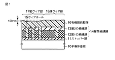
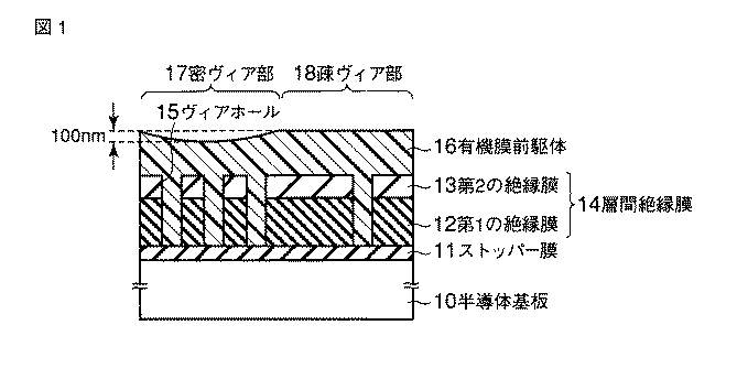
まず、図1に示すように、ストッパー膜11、第1の絶縁膜12および第2の絶縁膜13を、CVD法あるいはスピン塗布法などにより半導体基板10の上に順次形成する。第1の絶縁膜12と第2の絶縁膜13とによって、層間絶縁膜14が構成される。半導体基板10には、素子および下層配線(図示せず)が形成されている。第1の絶縁膜12および第2の絶縁膜13には、リソグラフィーおよびドライエッチング(RIE)によりヴィアホール15を形成する。さらに、有機成分と溶剤とを含む溶液を全面に塗布して、塗膜を形成する。以下に説明するような温度で第1のベークを施して有機膜前駆体16を得、さらに、CMPおよび第2の温度での第2のベークを行なって有機膜(第1の有機膜)を得る。
First, as shown in FIG. 1, a
ヴィアホール15が設けられた第2の絶縁膜13上に溶液を塗布して塗膜を形成する際、この溶液がヴィアホール15で消費される。その結果、図1に示されるように、密ヴィア部17における塗膜の膜厚は、疎ヴィア部18あるいはフィールド上と比べて100nm程度薄くなってしまう。
When a solution is applied on the second
有機膜前駆体16の表面の段差は、その上に形成される膜にも反映するので、最上層に設けられるレジスト膜の表面も平坦とはならない。レジスト膜の膜厚バラツキは、引き続いて行なわれる配線溝パターンのリソグラフィー工程においてフォーカスエラーの原因となる。本実施形態においては、塗膜を形成後に、特定の温度でのベークとレジストCMPとを行なって、最終的に得られるレジスト膜の膜厚が均一となるように平坦性を確保する。
Since the step on the surface of the
有機膜前駆体16の形成には、埋め込み特性に優れるノボラック樹脂を主成分とする樹脂を用いることが好ましい。例えば、i線用レジスト(例えば、JSR製IX370G)、ArFエキシマレーザーの反射防止膜用樹脂(例えば、JSR製ODL−50)等を用いることができる。また、加工変換差が小さく、ArFエキシマレーザーを用いたリソグラフィーにも反射防止膜として機能しうるシクロヘキサノンを主成分とする有機膜(例えば、JSR製CT01、CT08)を用いてもよい。
For the formation of the
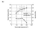
ノボラック樹脂等の有機成分を含む膜の硬度は、ベーク温度によって制御することができる。その関係を図2のグラフに示す。同グラフには、有機膜前駆体の平均硬度(Ave.)およびそのバラツキ(Max−Min)を示した。 The hardness of the film containing an organic component such as a novolak resin can be controlled by the baking temperature. The relationship is shown in the graph of FIG. The graph shows the average hardness (Ave.) of the organic film precursor and its variation (Max-Min).
ここでは、ノボラック樹脂を用いて膜を形成し、その硬度は、硬度測定装置(コベルコ社製、ナノインデンター)により測定した。具体的には、1cm四方の領域内を15ポイント測定して、平均硬度(Ave.)を求めた。硬度のバラツキは、その最大値(Max.)と最小値(Min.)との差である。 Here, a film was formed using a novolac resin, and the hardness thereof was measured with a hardness measuring device (manufactured by Kobelco, nanoindenter). Specifically, 15 points were measured in a 1 cm square region, and the average hardness (Ave.) was obtained. Hardness variation is the difference between the maximum value (Max.) And the minimum value (Min.).
一般に有機成分を含む膜は、ベーク温度を高めると、ポリマーの架橋が始まり、架橋終了温度を越えるとポリマーの架橋が終了して、非常に硬度の高い膜が得られる。ここで用いたノボラック樹脂は、150℃付近から架橋が開始して、280℃付近で架橋が終了する。図2のグラフに示されるように、ベーク温度が300℃の場合、得られた有機膜の平均硬度は0.5GPa程度である。このとき、硬度のバラツキは0.1GPa以下と小さいものの、平均硬度が0.5GPa程度以上の有機膜は、樹脂粒子で研磨することができない。 Generally, in a film containing an organic component, when the baking temperature is increased, the crosslinking of the polymer starts, and when the crosslinking end temperature is exceeded, the crosslinking of the polymer is terminated, and a film having very high hardness is obtained. The novolak resin used here starts to crosslink at around 150 ° C. and crosslink ends at around 280 ° C. As shown in the graph of FIG. 2, when the baking temperature is 300 ° C., the average hardness of the obtained organic film is about 0.5 GPa. At this time, although the variation in hardness is as small as 0.1 GPa or less, an organic film having an average hardness of about 0.5 GPa or more cannot be polished with resin particles.
したがって、本発明の実施形態においては、第1のベークが行なわれる第1の温度は、架橋が終了しない温度であることが必要である。例えばノボラック樹脂の場合、第1の温度は、90〜160℃の範囲が好ましい。こうした温度範囲内であれば、架橋が終了することなく、しかも樹脂粒子での研磨に適切な有機膜前駆体が得られる。 Therefore, in the embodiment of the present invention, the first temperature at which the first baking is performed needs to be a temperature at which the crosslinking is not completed. For example, in the case of a novolac resin, the first temperature is preferably in the range of 90 to 160 ° C. Within such a temperature range, the organic film precursor suitable for polishing with the resin particles can be obtained without completing the crosslinking.
なお、ノボラック樹脂を主成分とするi線用レジストの場合は、乳酸エチルおよび3−エトキシプロピオン酸エチル等の溶剤に溶解して塗膜の形成に用いられる。後述するように、第2のベークにおいては溶剤が除去されるので、この第2のベークが行なわれる第2の温度は、溶剤の種類に応じて選択することができる。例えば、前述の乳酸エチルおよび3−エトキシプロピオン酸エチルの場合には、250℃程度の加熱で除去することができる。溶剤を確実に除去するとともに、ノボラック樹脂が分解しないことから、第2の温度は、250〜400℃の範囲内が好ましい。 In the case of an i-line resist containing a novolak resin as a main component, it is dissolved in a solvent such as ethyl lactate and ethyl 3-ethoxypropionate and used to form a coating film. As will be described later, since the solvent is removed in the second baking, the second temperature at which the second baking is performed can be selected according to the type of the solvent. For example, in the case of the above-mentioned ethyl lactate and ethyl 3-ethoxypropionate, it can be removed by heating at about 250 ° C. The second temperature is preferably in the range of 250 to 400 ° C. because the solvent is surely removed and the novolac resin is not decomposed.
上述したような第1の温度で第1のベークを行なって、有機膜前駆体16が得られる。その後、層間絶縁膜14上の有機膜前駆体16を除去して、図3に示すようにヴィアホール15内に選択的に残置する。
The
第2の絶縁膜13上の有機膜前駆体16の除去は、樹脂粒子を含有するスラリーを用いたCMPにより行なう。具体的には、研磨布として例えばIC1000/Suba400(ロデール・ニッタ社製)を用い、図4に示されるように、研磨布31が貼付されたターンテーブル30を10〜70rpmで回転させつつ、半導体ウェハー32を保持したトップリング33を10〜70gf/cm2の研磨荷重で当接させる。トップリング33の回転数は20〜50rpmとすることができ、研磨布31上には、スラリー供給ノズル35から30〜1000cc/minの流量でスラリー37を供給する。なお、図4には、水供給ノズル34、ドレッサー36も併せて示してある。
Removal of the
ここで用いられるスラリーは、基本的には樹脂粒子を水に分散させて構成されるものであり、樹脂粒子について詳細に説明する。 The slurry used here is basically constituted by dispersing resin particles in water, and the resin particles will be described in detail.
樹脂粒子としては、PMMA(ポリメチルメタクリレート)等のアクリル系樹脂、PST(ポリスチレン)系樹脂、スチレンアクリル共重合樹脂、ユリア樹脂、メラミン樹脂、ポリアセタール樹脂、およびポリカーボネイト樹脂からなる群から選択される粒子を用いることができる。樹脂粒子は、これらの複合樹脂から構成されてもよい。特に、有機膜前駆体のCMPに適した硬度・弾性を有することから、PMMA、PSTあるいはスチレンアクリル共重合樹脂などが好ましい。 As the resin particles, particles selected from the group consisting of acrylic resins such as PMMA (polymethyl methacrylate), PST (polystyrene) resins, styrene acrylic copolymer resins, urea resins, melamine resins, polyacetal resins, and polycarbonate resins Can be used. The resin particles may be composed of these composite resins. In particular, PMMA, PST, styrene acrylic copolymer resin, or the like is preferable because it has hardness and elasticity suitable for CMP of the organic film precursor.
樹脂粒子は、架橋構造を有してもよい。樹脂粒子が架橋構造を有することで樹脂粒子の硬度・弾性を高めることができ、有機膜前駆体のCMPにより適した樹脂粒子とすることができる。架橋構造を有する樹脂粒子は、例えば樹脂粒子の原料として多官能性単量体を用いることによって、作製することができる。多官能性単量体とは、2個以上の重合性不飽和結合を有する単量体であり、例えば、ジビニル芳香族化合物および多価(メタ)アクリレート等を挙げることができる。 The resin particles may have a crosslinked structure. Since the resin particles have a crosslinked structure, the hardness and elasticity of the resin particles can be increased, and the resin particles can be made more suitable for CMP of the organic film precursor. Resin particles having a crosslinked structure can be produced, for example, by using a polyfunctional monomer as a raw material for the resin particles. The polyfunctional monomer is a monomer having two or more polymerizable unsaturated bonds, and examples thereof include a divinyl aromatic compound and a polyvalent (meth) acrylate.
こうした樹脂粒子の表面には、アニオン系、カチオン系、両性系、および非イオン系官能基から選択される少なくとも1種の官能基が導入され得る。アニオン系官能基としては、例えば、カルボン酸型、スルホン酸型、硫酸エステル型、リン酸エステル型等が挙げられ、カチオン系官能基としては、例えば、アミン塩型、第4級アンモニウム塩型等が挙げられる。両性系官能基としては、例えば、アルカノールアミド型、カルボキシベタイン型、およびグリシン型等が挙げられ、非イオン系官能基としては、例えば、エーテル型、エステル型等が挙げられる。粒子の製造が容易であることから、カルボキシル基が特に好ましい。 At least one type of functional group selected from anionic, cationic, amphoteric, and nonionic functional groups can be introduced on the surface of the resin particles. Examples of the anionic functional group include a carboxylic acid type, a sulfonic acid type, a sulfate ester type, and a phosphate ester type. Examples of the cationic functional group include an amine salt type and a quaternary ammonium salt type. Is mentioned. Examples of the amphoteric functional group include alkanolamide type, carboxybetaine type, and glycine type, and examples of the nonionic functional group include ether type and ester type. A carboxyl group is particularly preferred because of easy particle production.
樹脂粒子を安定して分散させるためには、ζ電位の絶対値が所定値以上であることが好ましい。具体的には、ζ電位の絶対値は20mV程度以上であることが望まれる。官能基の割合を0.05mol/L程度以上とすることによって、これを達成することができる。場合によっては、2種以上の官能基が同時に存在していてもよい。官能基が樹脂粒子の表面に存在することによって、界面活性剤を添加することなく、樹脂粒子同士の電気的反発力により分散性を高めることができる。 In order to stably disperse the resin particles, the absolute value of the ζ potential is preferably a predetermined value or more. Specifically, it is desirable that the absolute value of the ζ potential is about 20 mV or more. This can be achieved by setting the functional group ratio to about 0.05 mol / L or more. In some cases, two or more functional groups may be present simultaneously. When the functional group is present on the surface of the resin particles, the dispersibility can be enhanced by the electric repulsion between the resin particles without adding a surfactant.
例えば、官能基としてカルボキシル基(COOH)を表面に有する樹脂粒子の場合、カルボキシル基はスラリー中でCOOH→COO-+H+と解離して、樹脂粒子の表面がマイナスに帯電する。このため、電気的反発力により粒子同士の凝集を防ぎ、分散性を高めて寿命を長くすることが可能である。 For example, in the case of resin particles having a carboxyl group (COOH) on the surface as a functional group, the carboxyl group dissociates from COOH → COO − + H + in the slurry, and the surface of the resin particle is negatively charged. For this reason, it is possible to prevent the particles from agglomerating by the electric repulsive force, to increase the dispersibility and to extend the life.
カルボキシル基(COOH)を表面に有する架橋PMMA粒子は、例えば、次のような手法により合成することができる。まず、メチルメタクリレート、メタクリル酸、ジビニルベンゼン、ラウリル硫酸アンモニウムおよび過硫酸アンモニウムを、十分な量のイオン交換水とともにフラスコ中に収容する。これを、窒素ガス雰囲気下、攪拌しつつ70〜80℃に昇温して、6〜8時間重合させる。こうして、表面にカルボキシル基を有するPMMA粒子が得られる。原料となる単量体の量、反応温度や時間、その他の製造条件を変更することによって、例えば0.01〜5μmの範囲内で樹脂粒子の平均粒子径を制御することができる。 Crosslinked PMMA particles having a carboxyl group (COOH) on the surface can be synthesized, for example, by the following method. First, methyl methacrylate, methacrylic acid, divinylbenzene, ammonium lauryl sulfate and ammonium persulfate are placed in a flask together with a sufficient amount of ion-exchanged water. This is heated to 70 to 80 ° C. with stirring in a nitrogen gas atmosphere and polymerized for 6 to 8 hours. In this way, PMMA particles having a carboxyl group on the surface are obtained. By changing the amount of monomer as a raw material, reaction temperature and time, and other production conditions, the average particle diameter of the resin particles can be controlled within a range of 0.01 to 5 μm, for example.
なお、樹脂粒子の平均粒子径は、例えば、TEM観察、SEM観察、粒度分布測定といった手法により測定することができる。 The average particle diameter of the resin particles can be measured by a technique such as TEM observation, SEM observation, or particle size distribution measurement.
上述したような官能基を表面に有する樹脂粒子を水中に分散させることによって、本実施形態に用いるスラリーが得られる。水としては、イオン交換水、純水等を用いることができる。樹脂粒子は、スラリー中0.01〜10wt%程度の濃度となるよう分散させることが好ましい。0.01wt%未満の場合には、十分に高い速度で有機膜前駆体を研磨することが困難となる。一方、10wt%を越えると、有機膜が埋め込まれるSiN、SiO2等といった絶縁膜との選択比が取れなくなるおそれがある。なお、樹脂粒子の濃度は、0.1〜5wt%がより好ましく、0.3〜3wt%が最も好ましい。 The slurry used for this embodiment is obtained by disperse | distributing the resin particle which has a functional group on the surface as mentioned above in water. As water, ion exchange water, pure water, or the like can be used. The resin particles are preferably dispersed so as to have a concentration of about 0.01 to 10 wt% in the slurry. When it is less than 0.01 wt%, it becomes difficult to polish the organic film precursor at a sufficiently high rate. On the other hand, if it exceeds 10 wt%, there is a possibility that the selection ratio with the insulating film such as SiN or SiO 2 in which the organic film is embedded cannot be obtained. The concentration of the resin particles is more preferably 0.1 to 5 wt%, and most preferably 0.3 to 3 wt%.
スラリー中には、酸化剤、有機酸あるいは界面活性剤といった添加剤を、通常用いられている量で必要に応じて配合してもよい。 In the slurry, additives such as an oxidant, an organic acid, or a surfactant may be blended as necessary in a commonly used amount.
本発明の実施形態に用いられるスラリーのpHは、2以上8以下であることが望まれる。pHが2未満の場合には、COOH等の官能基が解離しづらく分散性が悪化するおそれがある。一方、pHが8を越えると、レジスト膜等の有機膜前駆体への化学的ダメージが大きくなってディッシングが増大する傾向がある。 The pH of the slurry used in the embodiment of the present invention is desirably 2 or more and 8 or less. When the pH is less than 2, the functional group such as COOH is difficult to dissociate and the dispersibility may be deteriorated. On the other hand, if the pH exceeds 8, chemical damage to an organic film precursor such as a resist film tends to increase and dishing tends to increase.
pH調整剤を適宜配合することによって、上述した範囲のpHに調整することができる。pH調整剤としては、例えば、硝酸、リン酸、塩酸、硫酸、およびクエン酸等を用いることができる。 It can adjust to pH of the range mentioned above by mix | blending a pH adjuster suitably. As the pH adjuster, for example, nitric acid, phosphoric acid, hydrochloric acid, sulfuric acid, citric acid and the like can be used.
本実施形態においては、樹脂粒子の平均粒子径は、有機膜が埋め込まれる凹部の径より大きいことが望まれる。具体的には、0.1μm以上5μm以下が好ましい。0.1μm未満の場合には、有機膜が埋め込まれる凹部、ここでは絶縁膜に設けられたヴィアホール内に粒子が侵入しやすくなって、ディッシングが拡大する傾向にある。一方、5μmを越えると粒子の分散性を制御するのが困難になり、スラリーが沈降しやすくなる。樹脂粒子の平均粒子径は、0.1μm以上2μm以下がより好ましい。 In the present embodiment, it is desirable that the average particle diameter of the resin particles is larger than the diameter of the recess in which the organic film is embedded. Specifically, it is preferably 0.1 μm or more and 5 μm or less. When the thickness is less than 0.1 μm, the particles tend to enter the recesses in which the organic film is embedded, here, the via holes provided in the insulating film, and the dishing tends to expand. On the other hand, if it exceeds 5 μm, it becomes difficult to control the dispersibility of the particles, and the slurry tends to settle. The average particle diameter of the resin particles is more preferably 0.1 μm or more and 2 μm or less.
こうしたスラリーを用いて所定時間の研磨を行なうことによって、図3に示したようにヴィアホール15内に有機膜前駆体16が選択的に残置され、第2の絶縁膜13が露出する。有機膜前駆体16のディッシングは、20nm以下に低減することができ、第2の絶縁膜13のロスもほぼゼロに抑制することができる。
By performing polishing for a predetermined time using such slurry, the
図3に示したようにヴィアホール15内に有機膜前駆体16を残置した後、第1の温度より高い第2の温度で第2のベークを行なう。この第2のベークにより有機膜前駆体16中の溶剤を除去し、図5に示すように有機膜(第1の有機膜)19を得る。上述したように例えば、溶剤としての乳酸エチルまたは3−エトキシプロピオン酸エチルにノボラック樹脂を溶解して用いる場合には、第2の温度は、250〜400℃程度とすることができる。
After leaving the
ヴィアホール15内に埋め込まれた有機膜19は、第2の温度で第2のベークが行なわれたことによって溶剤が除去されている。溶剤が実質的に存在しないことに起因して、後の工程で、有機膜19の上に塗膜が形成された場合でも、平坦性が損なわれることはない。溶剤が残留している有機膜前駆体の上には、表面が平坦な塗膜を形成することができない。平坦化された有機膜前駆体の内部に残留した溶剤は、塗膜中の溶剤と反応して平坦化の効果が失われてしまう。その結果、塗膜の表面には、段差が生じることになる。
The
本実施形態においては、ヴィアホール15内に埋め込まれた有機膜19中には溶剤が実質的に存在しないので、こうした問題は回避される。すなわち、図6に示すように第2の有機膜20は、平坦な表面をもって第1の有機膜19の上に形成される。第1の有機膜19とこの上の第2の有機膜20とによって、下層膜21が構成される。
In the present embodiment, since the solvent is not substantially present in the
下層膜21は、第1の有機膜19上に第2の有機膜20となる塗膜を形成した後、その上に中間層22を形成する前に、250℃以上の温度でベークすることが好ましい(第3のベーク)。この第3のベークによって、下層膜21のエッチング耐性を高めることができる。温度が高すぎる場合には、第1および第2の有機膜19,20中の有機成分が分解するおそれがあるので、ベークの温度の上限は400℃程度にとどめることが望まれる。
The lower layer film 21 may be baked at a temperature of 250 ° C. or higher after the coating film to be the second
下層膜21の上には、図6に示すように中間層22およびレジスト膜23が順次堆積される。下層膜21の表面が平坦であるので、この上に形成されるレジスト膜23の表面も平坦とすることができる。ヴィア密度によらず段差が抑制されるので、こうしたレジスト膜23にパターン露光を行なった際には、レジスト膜の露光量依存性(ベストフォーカス)は、実質的にヴィア密度には依存しない。その結果、リソグラフィーのフォーカスマージンを拡大することができた。
On the lower film 21, an
露光後のレジスト膜23を現像液により現像してレジストパターン(図示せず)を得、これをエッチングマスクとして中間層22、第2の有機膜20を順次エッチングして、図7に示すように配線溝パターン24を形成する。このとき、レジスト膜23は除去され、さらに第2の絶縁膜13を貫通し、第1の絶縁膜12の途中まで配線溝パターン24を転写する際には、中間層22も除去される。
The exposed resist film 23 is developed with a developer to obtain a resist pattern (not shown), and the
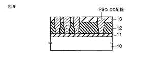
その後、ヴィアホール15内に埋め込まれた第1の有機膜19を、第2の絶縁膜13の上の第2の有機膜20とともに剥離して、図8に示すようにヴィアホール15と連通する配線溝25が形成される。ヴィアホール15内のストッパー膜11を除去した後、TaNなどからなるバリアメタル膜(図示せず)を介してCu膜をメッキ法あるいはスパッタ法などにより成膜する。さらに、CMPを行なうことによりフィールド上のCuを除去して、図9に示すCuデュアルダマシン配線26が形成される。
Thereafter, the first
本発明の他の実施形態においては、凹部としての配線溝パターン内に有機膜を埋め込むこともできる。図10乃至図25を参照して、配線溝パターン内に有機膜を形成する例を説明する。 In another embodiment of the present invention, an organic film can be embedded in a wiring groove pattern as a recess. An example of forming an organic film in the wiring groove pattern will be described with reference to FIGS.
まず、図10に示すように、素子(図示せず)が形成された半導体基板40上に、有機系絶縁膜44、無機材料を含む第1、第2および第3のハードマスク45,46,および47を順次形成し、第3のハードマスク47に凹部としての配線溝パターン48aおよび48bを形成する。図示する例においては、有機系絶縁膜44は、第1の有機系絶縁膜42および第2の有機系絶縁膜43の二層構造であり、これらの下層にはエッチングストッパー膜41が形成されている。
First, as shown in FIG. 10, an organic insulating
図示していないが、エッチングストッパー膜41と半導体基板40との間には、第1の配線層が埋め込み形成された層間絶縁膜が設けられる。層間絶縁膜としては、例えば酸化シリコン膜を用いることができ、バリア層を介してCuを埋め込むことによって第1の配線層が形成される。エッチングストッパー膜41は、このCuの拡散を防止する作用も有しており、例えばSiN膜を堆積して形成することができる。
Although not shown, an interlayer insulating film in which a first wiring layer is embedded is provided between the
第1の有機系絶縁膜42および第2の有機系絶縁膜43としては、それぞれSiOCおよびPAE(ポリアリールエーテル)をPE−CVD(plasma enhancement Chemical Vapor Deposition)法により堆積して形成することができる。有機膜の材料としては、ポリアリールエーテル(アライドシグナル社製(商品名:FLARE)、ダウケミカル社製(商品名:SiLK))、ベンゾシクロブテン(ダウケミカル社製)およびポリイミド等を用いることもできる。第1および第2の有機系絶縁膜42,43の膜厚は特に限定されず、50〜400nmの範囲内で選択すればよい。
The first organic insulating
なお、CVD法により形成される有機膜の材料としては、コーラル(商品名、ノベラス社製)、オーロラ(商品名、エー・エス・エム社製)、およびブラックダイアモンド(商品名、アプライドマテリアル社製)等が知られており、塗布法により形成される有機膜の材料としては、メチルシルセスキオキサン等が知られている。 In addition, as a material of the organic film formed by the CVD method, coral (trade name, manufactured by Novellus), aurora (trade name, manufactured by ASM), and black diamond (trade name, manufactured by Applied Materials) ) And the like, and as a material for an organic film formed by a coating method, methylsilsesquioxane or the like is known.
第1および第2の有機系絶縁膜42,43から構成される有機系絶縁膜44上には、CVD法またはPVD(Physical Vapor Deposition)法によって、シラン系SiO2膜を第1のハードマスク45として形成する。第2のハードマスク46としては、例えばSiN膜を用いることができ、第3のハードマスク47は、例えばTEOS(テトラエトキシシラン)を用いて形成することができる。なお、いずれの材料を用いて、第1、第2および第3のハードマスク45,46,47を形成してもよく、またさらに、シリコン炭化膜によりハードマスクを形成することもできる。
On the organic insulating
レジストパターン(図示せず)を第3のハードマスク47上に形成し、C4F8/CO/Arのガスを用いて、この第3のハードマスク47をドライエッチングすることによって、図10に示すように凹部としての配線溝パターン48aおよび48bを形成する。配線溝パターン48aおよび48bの幅は、それぞれ3μmおよび0.4μmとすることができる。
A resist pattern (not shown) is formed on the third
配線溝パターン48a,48bが設けられた第3のハードマスク47上には、図11に示すように有機膜前駆体49を形成する。有機膜前駆体49は、底面においてはSiNからなる第2のハードマスク46と接触することになる。有機膜前駆体49の形成に当たっては、まず、ノボラック樹脂を主成分とするレジスト(JSR製IX370G)を塗布して、膜厚0.1〜3μm程度の塗膜を形成する。
An
すでに説明したように、ノボラック樹脂の架橋は250℃程度で終了するので、これより低い温度(第1の温度)で第1のベークを行なって、有機膜前駆体49を得る。
As already described, since the crosslinking of the novolak resin is completed at about 250 ° C., the
有機膜前駆体49の表面には、図11に示されるように、配線溝パターン48aを反映した段差50が生じる。本実施形態においては、CMPを用いて配線溝パターン48a,48b内に有機膜前駆体49を残置させた後、第1の温度より高い第2の温度で第2のベークを行なう。その後、再度有機膜を塗布して下層膜を形成することによって、フォーカスエラーを抑制する。ノボラック樹脂を主成分とする有機膜は、例えばシクロヘキサノンを主成分とする有機膜よりも、平坦化を容易に行なうことができる点で好ましい。さらに、ノボラック樹脂を主成分とする有機膜は、シクロヘキサノンを主成分とする有機膜よりも第3のハードマスク47との密着力が強く、CMP時の剥がれも比較的少ない。
As shown in FIG. 11, a
有機膜前駆体49の平坦化は、樹脂粒子と水溶性高分子とを含有するスラリーを用いたCMPにより行なう。基本的には、図4を参照して説明したような手法により、有機膜前駆体49を平坦化することができる。所定時間の研磨を行なうことによって、図12に示すように配線溝パターン48a、48b内に有機膜前駆体49が残置され、第3のハードマスク47が露出する。また、研磨後の有機膜前駆体49表面におけるディッシングは、10nm以下に抑制することができる。
The planarization of the
有機膜前駆体49の平坦化に用いられるスラリーは、基本的には前述と同様の組成とすることができるが、水溶性高分子をさらに含有することが好ましい。
The slurry used for planarization of the
ただし、用いられる樹脂粒子の平均粒子径は、0.01μm以上5μm以下の範囲内であることが望まれる。水溶性高分子を含有することから、本実施形態においては、ヴィアホール内に有機膜を埋め込む場合よりも小さい樹脂粒子を用いることができる。樹脂粒子の平均粒子径が5μmを越える場合、あるいは0.01μm未満の場合には、粒子の分散性を制御するのが困難になり、スラリーが沈降しやすくなる。樹脂粒子の平均粒子径は、0.03μm以上0.5μm以下がより好ましい。こうした樹脂粒子は、すでに説明したような方法を用いて、原料となる単量体の量、反応温度や時間、その他の条件を適宜変更することによって合成することができる。 However, the average particle diameter of the resin particles used is desirably in the range of 0.01 μm or more and 5 μm or less. Since it contains a water-soluble polymer, in the present embodiment, smaller resin particles can be used than in the case where an organic film is embedded in a via hole. When the average particle diameter of the resin particles exceeds 5 μm or less than 0.01 μm, it becomes difficult to control the dispersibility of the particles, and the slurry tends to settle. The average particle diameter of the resin particles is more preferably 0.03 μm or more and 0.5 μm or less. Such resin particles can be synthesized by appropriately changing the amount of monomer as a raw material, the reaction temperature and time, and other conditions using the method described above.
また、樹脂粒子の濃度は、スラリー中0.01〜10wt%程度であることが好ましい。0.01wt%未満の場合には、研磨速度が極端に低下するおそれがある。一方、10wt%を越えると、ディッシングを許容範囲内に抑制するのが困難になる。樹脂粒子の濃度は、0.1〜5wt%がより好ましく、0.3〜3wt%が最も好ましい。 Moreover, it is preferable that the density | concentration of a resin particle is about 0.01-10 wt% in a slurry. If it is less than 0.01 wt%, the polishing rate may be extremely reduced. On the other hand, if it exceeds 10 wt%, it becomes difficult to suppress dishing within an allowable range. The concentration of the resin particles is more preferably 0.1 to 5 wt%, and most preferably 0.3 to 3 wt%.
ここで、凹部としての配線溝パターンのサイズは、通常、数μmであり、樹脂粒子のサイズより大きい。したがって、こうした凹部を有する絶縁膜の上に形成された有機膜前駆体を平坦化する際、樹脂粒子が配線溝パターン内に侵入してディッシングが拡大してしまうおそれがある。その結果、平坦性を確保することができず、引き続いて行なわれる孔パターンのリソグラフィー工程においてフォーカスエラーの原因となる。 Here, the size of the wiring groove pattern as the recess is usually several μm, which is larger than the size of the resin particles. Therefore, when the organic film precursor formed on the insulating film having such a recess is flattened, the resin particles may enter the wiring groove pattern and the dishing may be enlarged. As a result, flatness cannot be ensured, which causes a focus error in the subsequent lithography process of the hole pattern.
ディッシングを抑制するために、研磨対象となる有機膜前駆体の硬度を高めることが考えられる。しかしながら、本実施形態において研磨に用いられる樹脂粒子は、非常に柔らかく研磨力が乏しいことから、硬度の高い膜を研磨することはできない。CMP前に行なわれる第1のベークの温度は、有機成分の架橋が終了しない温度に規定されるので、高温でのベークは採用することができない。 In order to suppress dishing, it is conceivable to increase the hardness of the organic film precursor to be polished. However, since the resin particles used for polishing in the present embodiment are very soft and have poor polishing power, it is not possible to polish a film having high hardness. Since the temperature of the first baking performed before CMP is regulated to a temperature at which the crosslinking of the organic components is not completed, baking at a high temperature cannot be employed.
本実施形態においては、スラリー中に水溶性高分子を配合することによって、ディッシングの抑制が可能となる。水溶性高分子は、研磨対象である有機膜前駆体の表面に吸着して、樹脂粒子から保護する作用を有するが、このメカニズムについては後述する。 In the present embodiment, dishing can be suppressed by blending a water-soluble polymer in the slurry. The water-soluble polymer has an action of adsorbing to the surface of the organic film precursor to be polished and protecting it from the resin particles. This mechanism will be described later.
水溶性高分子としては、例えばメチルセルロース、メチルヒドロキシエチルセルロース、メチルヒドロキシプロピルセルロース、ヒドロキシエチルセルロース、ヒドロキシプロピルセルロース、カルボキシメチルセルロース、カルボキシエチルセルロース、カルボキシメチルヒドロキシエチルセルロース等のセルロース類;キトサン等の多糖類、ポリエチレングリコール、ポリエチレンイミン、ポリビニルピロリドン、ポリビニルアルコール、ポリアクリル酸およびその塩、ポリアクリルアミド、ポリエチレンオキシド等などを用いることができる。これらの水溶性高分子は、単独でまたは2種以上を混合して使用することができる。 Examples of water-soluble polymers include celluloses such as methylcellulose, methylhydroxyethylcellulose, methylhydroxypropylcellulose, hydroxyethylcellulose, hydroxypropylcellulose, carboxymethylcellulose, carboxyethylcellulose, carboxymethylhydroxyethylcellulose; polysaccharides such as chitosan, polyethylene glycol, Polyethyleneimine, polyvinyl pyrrolidone, polyvinyl alcohol, polyacrylic acid and its salt, polyacrylamide, polyethylene oxide and the like can be used. These water-soluble polymers can be used alone or in admixture of two or more.
なかでも、高い平坦性が得られることから、ポリビニルアルコールおよびポリビニルピロリドンが好ましい。 Among these, polyvinyl alcohol and polyvinyl pyrrolidone are preferable because high flatness can be obtained.
水溶性高分子の平均分子量は、500〜1,000,000の範囲内が好ましい。500未満の場合には、研磨対象である有機膜前駆体との十分な相互作用を得ることができず、保護効果が小さくなって、ディッシングを抑制することが困難となる。一方、1,000,000を越えると、吸着効果が大きすぎて研磨速度が低下するおそれがある。さらに、粘性が高くなりすぎて、スラリー供給が困難になるおそれがある。水溶性高分子の平均分子量は、1,000〜500,000がより好ましく、5,000〜300,000が最も好ましい。 The average molecular weight of the water-soluble polymer is preferably in the range of 500 to 1,000,000. If it is less than 500, sufficient interaction with the organic film precursor to be polished cannot be obtained, the protective effect is reduced, and it becomes difficult to suppress dishing. On the other hand, if it exceeds 1,000,000, the adsorption effect is too great and the polishing rate may decrease. Furthermore, the viscosity becomes too high, and there is a possibility that the slurry supply becomes difficult. The average molecular weight of the water-soluble polymer is more preferably 1,000 to 500,000, and most preferably 5,000 to 300,000.
水溶性高分子の濃度は、スラリー中0.001〜10wt%の範囲内であることが好ましい。0.001wt%未満の場合には、ディッシングを抑制することが困難となる。一方、10wt%を越える場合には、有機膜前駆体へ過度に吸着して、研磨速度が極端に低下するおそれがある。水溶性高分子の濃度は、0.01〜1wt%がより好ましく、0.05〜0.5wt%が最も好ましい。 The concentration of the water-soluble polymer is preferably in the range of 0.001 to 10 wt% in the slurry. If it is less than 0.001 wt%, it becomes difficult to suppress dishing. On the other hand, if it exceeds 10 wt%, it is excessively adsorbed on the organic film precursor, and the polishing rate may be extremely reduced. The concentration of the water-soluble polymer is more preferably 0.01 to 1 wt%, and most preferably 0.05 to 0.5 wt%.
水溶性高分子と樹脂粒子とを含有するスラリーを用いて研磨が行なわれるので、配線溝パターンに対するレジスト膜のディッシングを20nm以下に抑制することが可能となり、平坦性が格段に改善される。これは、スラリー中に水溶性高分子が含有されることに起因するものであり、次のように説明される。 Since polishing is performed using a slurry containing a water-soluble polymer and resin particles, dishing of the resist film with respect to the wiring groove pattern can be suppressed to 20 nm or less, and the flatness is remarkably improved. This is caused by the fact that the water-soluble polymer is contained in the slurry, and is explained as follows.
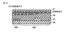
水溶性高分子が含有されずに樹脂粒子が含有されたスラリーを用いて有機膜前駆体のCMPが行なわれる場合には、高摩擦で有機膜前駆体を剥ぎ取りながら研磨が進行する。これに対して、図13に示されるように、樹脂粒子60とともに水溶性高分子61が含有されたスラリーでは、水溶性高分子61がウェハーと研磨布31との間に潤滑油のように機能して摩擦を軽減し、段階的に有機膜前駆体49を除去する研磨機構に変化する。これに加えて、水溶性高分子61が有機膜前駆体49表面に吸着し、樹脂粒子60から表面を保護する。この結果、樹脂粒子60に水溶性高分子61を添加したスラリーを用いることによって平坦性を確保できるとともに、樹脂粒子60の軟性によりスクラッチの発生を抑制することができる。
When CMP of an organic film precursor is performed using a slurry containing resin particles without containing a water-soluble polymer, polishing proceeds while peeling off the organic film precursor with high friction. On the other hand, as shown in FIG. 13, in the slurry containing the water-soluble polymer 61 together with the
さらに、砥粒として用いられるのは有機膜前駆体と同質の樹脂粒子であるので、CMP後に残留しても、その後の加工においてアルミナ粒子のようにエッチングマスクとなることがない。このため、粒子残留に対するリスクを低減することが可能となる。この結果、後工程のヴィアホールのリソグラフィーにおいて、フォーカスエラーを低減し、歩留まりを格段に向上させることが可能となる。 Furthermore, since resin particles of the same quality as the organic film precursor are used as the abrasive grains, even if they remain after CMP, they do not become an etching mask like alumina particles in subsequent processing. For this reason, it becomes possible to reduce the risk with respect to residual particles. As a result, it becomes possible to reduce the focus error and significantly improve the yield in the lithography of via holes in the subsequent process.
なお、水溶性高分子のみで研磨を行なった場合には、上述したようなメカニズムによりディッシングを20nm以下に抑制することは可能であるものの、研磨速度が非常に遅くなる。したがって、凹部としての配線溝パターンに有機膜を埋め込む際には、実用的な研磨速度を得るために、水溶性高分子は樹脂粒子と併用されることが必要である。 Note that when polishing is performed only with the water-soluble polymer, the polishing rate becomes very slow although the dishing can be suppressed to 20 nm or less by the mechanism described above. Therefore, when an organic film is embedded in the wiring groove pattern as the recess, the water-soluble polymer needs to be used in combination with the resin particles in order to obtain a practical polishing rate.
有機膜前駆体49の研磨は、異なるスラリーを用いて二段階で行なってもよい。第1の研磨においては、第1のスラリーを用いて図14に示すように有機膜前駆体49を平坦化し、次いで、第2のスラリーを用いた第2の研磨において、図12に示したように第3のハードマスク47を露出する。
The polishing of the
第2のスラリーは、樹脂粒子および水溶性高分子の少なくとも一方の濃度を変更する以外は、第1のスラリーと同様の組成とすることができる。この場合、第2のスラリーに含有される樹脂粒子の量は、第1のスラリーより少なく、第2のスラリーに含有される水溶性高分子の量は、第1のスラリーより多い。ディッシングを確実に抑制しつつ十分に大きな研磨速度を確保するためには、樹脂粒子の濃度および水溶性高分子の濃度を同時に変化させることが望まれる。 The second slurry can have the same composition as the first slurry except that the concentration of at least one of the resin particles and the water-soluble polymer is changed. In this case, the amount of resin particles contained in the second slurry is less than that of the first slurry, and the amount of water-soluble polymer contained in the second slurry is greater than that of the first slurry. In order to ensure a sufficiently high polishing rate while reliably suppressing dishing, it is desirable to simultaneously change the concentration of the resin particles and the concentration of the water-soluble polymer.
例えば、第1のスラリーにおける樹脂粒子の濃度を0.6〜1wt%とした場合には、第2のスラリーにおける樹脂粒子の濃度を0.1〜0.5wt%とする。さらに、第1のスラリーにおける水溶性高分子の濃度を0.01〜0.2wt%とし、第2のスラリーにおける水溶性高分子の濃度を0.25〜0.5wt%とする。 For example, when the concentration of the resin particles in the first slurry is 0.6-1 wt%, the concentration of the resin particles in the second slurry is 0.1-0.5 wt%. Furthermore, the concentration of the water-soluble polymer in the first slurry is set to 0.01 to 0.2 wt%, and the concentration of the water-soluble polymer in the second slurry is set to 0.25 to 0.5 wt%.
上述したように組成の異なる第1および第2のスラリーを用いることによって、第1の研磨においては、ディッシングが拡大するといった欠陥を回避しつつ十分に大きな速度で平坦化を達成するとともに、第2の研磨においては、ディッシングが再度発生するのを抑制することが可能となる。 By using the first and second slurries having different compositions as described above, in the first polishing, flattening is achieved at a sufficiently high speed while avoiding defects such as dishing being enlarged, and the second polishing. In this polishing, it is possible to suppress the occurrence of dishing again.
次いで、第1の温度より高い第2の温度で第2のベークを行なうことにより、有機膜前駆体49中の溶剤を除去するとともに架橋を終了させて、図15に示すように配線溝パターン48a,48bに埋め込まれた有機膜(第1の有機膜)51を得る。
Next, by performing a second baking at a second temperature higher than the first temperature, the solvent in the
さらに、図16に示すようにIX370Gを再度塗布して第2の有機膜52を形成して、第1の有機膜51および第2の有機膜52からなる下層膜53を得る。上述したような理由から、中間層54を形成する前に、下層膜53を250〜400℃程度での温度でベークすることが望まれる。続いて、中間層54としてのSOG(Spin on glass)膜、およびレジスト膜55を順次形成する。ここでは、第2の有機膜52は300nm程度の厚さで形成することができる。また、中間層54およびレジスト膜55の膜厚は、それぞれ100nm程度および200nm程度とすることができる。
Further, as shown in FIG. 16, IX370G is applied again to form the second organic film 52, and the lower layer film 53 composed of the first
下層膜53の表面が平坦であるので、この上に形成されるレジスト膜55の表面も平坦とすることができる。平坦な表面を有する下層膜53は、溶剤が除去された有機膜51の上に、第2の有機膜52を形成することによって、形成可能となったものである。
Since the surface of the lower layer film 53 is flat, the surface of the resist film 55 formed thereon can also be flat. The lower layer film 53 having a flat surface can be formed by forming the second organic film 52 on the
図12に示したように有機膜前駆体49を配線溝パターン内に選択的に残置した後、第2のベークを行なわずに第2の有機膜等を形成した場合の例を、図17に示す。図示するように有機膜前駆体49の上に第2の有機膜52を形成した場合には、これらによって構成される下層膜63の表面に段差が生じる。CMPを行なって有機膜前駆体49を平坦化しても、その効果は消失し、下層膜63表面に生じた段差は最上層のレジスト膜55の表面にも反映される。
FIG. 17 shows an example in which the second organic film or the like is formed without performing the second baking after the
すなわち、ここでの有機膜前駆体49は、CMP前に有機成分の架橋が終了しない温度でベークされており、このベーク条件下では、膜中の溶剤が十分に除去され難い。こうして十分除去されずに残留した溶剤に、第2の有機膜52用の溶剤が反応して有機膜前駆体49が溶解し、それによって下層膜63表面に段差が引き起こされたものと推測される。
That is, the
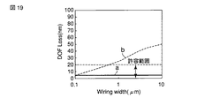
ここで、配線幅とレジスト膜表面の段差高さとの関係を図18に示す。図18(a)は、第2のベークを行なって溶剤を除去した本実施形態にかかる構造であり、図18(b)は、第2のベークを行なわずに第1の有機膜中に溶剤が残留する場合である。図18中、Iso.は孤立パターンを表わし、50%、65%、80%、90%、および95%は、配線の被覆率を表わす。配線の被覆率とは、配線幅とスペース幅との合計で配線幅を除した値であり、スペース幅が無限大の場合を孤立パターンと称する。 Here, the relationship between the wiring width and the step height on the resist film surface is shown in FIG. FIG. 18A shows a structure according to this embodiment in which the solvent is removed by performing the second baking, and FIG. 18B shows the solvent in the first organic film without performing the second baking. Is the case that remains. In FIG. Represents an isolated pattern, and 50%, 65%, 80%, 90%, and 95% represent wiring coverage. The wiring coverage is a value obtained by dividing the wiring width by the total of the wiring width and the space width, and a case where the space width is infinite is referred to as an isolated pattern.
図18(a)に示されるように、本実施形態の場合には、配線の幅や被覆率によらず、段差の高さは20nm以下に抑制されている。これに対し、第1の有機膜中に溶剤が残留した場合には、配線幅が大きくなるにしたがって、段差の高さが大きくなることが、図18(b)から明らかである。配線の被覆率が大きい場合もまた、段差の高さは増大することが示されている。したがって、異なる幅の配線が存在する場合や異なる被覆率で配線が形成される場合には、段差を抑制するのが困難である。 As shown in FIG. 18A, in the case of this embodiment, the height of the step is suppressed to 20 nm or less regardless of the width and coverage of the wiring. On the other hand, when the solvent remains in the first organic film, it is clear from FIG. 18B that the height of the step increases as the wiring width increases. It is also shown that the step height increases when the wiring coverage is large. Therefore, it is difficult to suppress the step when wirings with different widths exist or when wirings are formed with different coverages.
レジスト膜55表面の段差は、フォーカスエラーの増大にもつながる。図16に示したようにレジスト膜55が形成された後には、孔パターンを有する露光マスクを介して、KrFエキシマレーザーによりレジスト膜55に露光を行なう。孔パターンの径は、例えば60nm程度とすることができる。図18(a)を参照して説明したように、本実施形態においては、配線幅によらず段差が抑制されるので、配線幅3μmおよび0.4μm上のヴィア形成におけるフォーカスエラーは、10nm以下に抑制される。 The step on the surface of the resist film 55 leads to an increase in focus error. After the resist film 55 is formed as shown in FIG. 16, the resist film 55 is exposed by a KrF excimer laser through an exposure mask having a hole pattern. The diameter of the hole pattern can be about 60 nm, for example. As described with reference to FIG. 18A, in this embodiment, the step is suppressed regardless of the wiring width, so that the focus error in forming vias on the wiring widths of 3 μm and 0.4 μm is 10 nm or less. To be suppressed.
図19のグラフには、配線幅とフォーカスエラーとの関係を示す。本実施形態における結果は、実線aとして示され、配線幅によらずほぼ一定であることがわかる。その結果、パターンの寸法バラツキ、さらには歩留まりを格段に高めることが可能となった。なお、図19における破線bは、図17に示した構造の場合であり、配線幅が大きくなるにしたがって、フォーカスエラーが増大することがわかる。 The graph of FIG. 19 shows the relationship between the wiring width and the focus error. The result in this embodiment is shown as a solid line a, and it can be seen that the result is almost constant regardless of the wiring width. As a result, it has become possible to greatly increase the dimensional variation of the pattern and the yield. The broken line b in FIG. 19 is for the structure shown in FIG. 17, and it can be seen that the focus error increases as the wiring width increases.
露光後のレジスト膜55を現像液により現像して、レジストパターン(図示せず)を得、これをエッチングマスクとしてCHF3/O2ガスにより中間層54を加工する。さらに、NH3/O2/CH4ガスにより下層膜53を加工し、O2アッシングによりレジストパターンを剥離する。
The exposed resist film 55 is developed with a developer to obtain a resist pattern (not shown), and the
パターン化された中間層54および下層膜53をマスクとして、第2のハードマスク46および第1のハードマスク45にドライエッチングにより接続孔(ヴィアホール)を形成する。エッチングガスとしては、CHF3/Ar/O2のガスを用いることができる。第1のハードマスク45を加工する際、中間層54は除去される。さらに、NH3ガスを用いてドライエッチングを行ない、図20に示すように第2の有機系絶縁膜43にドライエッチングにより接続孔56を形成する。なお、下層膜53は、第2の有機系絶縁膜43を加工する際に除去される。
Using the patterned
次に、CH2F2/CF4/Ar/O2のガスを用いてドライエッチングを行ない、図21に示すように第2のハードマスク46に配線溝パターン48を形成する。図示するように、このとき接続孔56は、第1の有機系絶縁膜42の途中まで掘り進められる。さらに、C5F8/Ar/O2のガスを用いて第3のハードマスク47を除去するとともに、図22に示すように第1のハードマスク45に配線溝57を形成する。このとき、接続孔56は、エッチングストッパー膜41まで達する。このように二段階の加工工程によって、第1の有機系絶縁膜42に接続孔56が形成される。これは、確実に接続孔56を貫通できる点で有利である。
Next, dry etching is performed using a gas of CH 2 F 2 / CF 4 / Ar / O 2 to form a wiring groove pattern 48 in the second
次に、NH3のガスを用いたドライエッチングにより、図23に示すように第2の有機系絶縁膜43に配線溝57を形成する。最後に、CH2F2/CF4/Ar/O2のガスを用いて、図24に示すように第2のハードマスク46を除去する。このとき、接続孔56底部のエッチングストッパー膜41も除去される。
Next,
その後、接続孔56および配線溝57といった凹部の内面にバリア層(図示せず)を形成して、凹部内にCuを埋め込んだ後、第1のハードマスク45としての酸化シリコン膜上の余分なCu膜およびバリア層を除去する。こうして、図25に示されるように凹部内にCuダマシン配線を形成して、ハイブリッドデュアルダマシン配線58が形成される。
Thereafter, a barrier layer (not shown) is formed on the inner surfaces of the recesses such as the connection holes 56 and the
本実施形態においては、第1の有機膜51上に第2の有機膜52を形成して多層化する際に、有機膜前駆体49をCMPにより平坦化している。しかも、CMP後には、第2の温度でのベークが行なわれて、膜中の溶剤が実質的に除去されるので、この上に形成される塗膜によって平坦性が損なわれることはない。したがって、露光時におけるフォーカスエラーを10nm以下に抑制することができ、パターンの寸法バラツキ、さらには歩留まりを格段に高めることができる。
In the present embodiment, when the second organic film 52 is formed on the first
以下、具体例を示して本発明の実施形態を説明する。 Embodiments of the present invention will be described below with specific examples.
(実施例1)
本実施例では、凹部としてのヴィアホールに有機膜を埋め込む。まず、以下のようなスラリーを調製した。
Example 1
In this embodiment, an organic film is embedded in the via hole as the recess. First, the following slurry was prepared.
(スラリー1)
スチレン92重量部、メタクリル酸4重量部、ヒドロキシエチルアクリレート4重量部、ラウリル硫酸アンモニウム0.1重量部、過硫酸アンモニウム0.5重量部、およびイオン交換水400重量部を、容量2リットルのフラスコに収容した。窒素ガス雰囲気下で攪拌しながら70℃に昇温し、6時間重合させた。これによってカルボキシル基を表面に有し、平均粒子径200nmのPST粒子が得られた。
(Slurry 1)
92 parts by weight of styrene, 4 parts by weight of methacrylic acid, 4 parts by weight of hydroxyethyl acrylate, 0.1 part by weight of ammonium lauryl sulfate, 0.5 part by weight of ammonium persulfate and 400 parts by weight of ion-exchanged water are placed in a 2 liter flask. did. While stirring in a nitrogen gas atmosphere, the temperature was raised to 70 ° C. and polymerization was performed for 6 hours. As a result, PST particles having a carboxyl group on the surface and an average particle diameter of 200 nm were obtained.
このPST粒子を0.83wt%の濃度で純水に分散させて、スラリー1を得た。
The PST particles were dispersed in pure water at a concentration of 0.83 wt% to obtain
(スラリー2)
平均粒子径100nmのPST粒子を0.83wt%の濃度で純水に分散させて、スラリー2を得た。
(Slurry 2)
PST particles having an average particle diameter of 100 nm were dispersed in pure water at a concentration of 0.83 wt% to obtain
(スラリー3)
スチレン77重量部、アクリル酸3重量部、ジビニルベンゼン20重量部、ドデシルベンゼンスルホン酸アンモニウム2.0重量部、過硫酸アンモニウム1.0重量部、およびイオン交換水400重量部を、容量2リットルのフラスコに収容した。窒素ガス雰囲気下で攪拌しながら70℃に昇温し、6時間重合させた。これによって、カルボキシル基を有し、平均粒子径100nmの架橋PST粒子が得られた。
(Slurry 3)
A 2-liter flask containing 77 parts by weight of styrene, 3 parts by weight of acrylic acid, 20 parts by weight of divinylbenzene, 2.0 parts by weight of ammonium dodecylbenzenesulfonate, 1.0 part by weight of ammonium persulfate, and 400 parts by weight of ion-exchanged water. Housed in. While stirring in a nitrogen gas atmosphere, the temperature was raised to 70 ° C. and polymerization was performed for 6 hours. As a result, crosslinked PST particles having a carboxyl group and an average particle diameter of 100 nm were obtained.
この架橋PST粒子を、0.83wt%の濃度で純水に分散させて、スラリー3を得た。 The crosslinked PST particles were dispersed in pure water at a concentration of 0.83 wt% to obtain slurry 3.
(スラリー4)
平均粒子径200nmの架橋PST粒子を0.83wt%の濃度で純水に分散させて、スラリー4を得た。
(Slurry 4)
Crosslinked PST particles having an average particle diameter of 200 nm were dispersed in pure water at a concentration of 0.83 wt% to obtain slurry 4.
(スラリー5)
水溶性高分子としての分子量17600のポリビニルアルコールを、0.16wt%の量でスラリー1に加えてスラリー5を得た。
(Slurry 5)
A
(スラリー6)
平均粒子径50nmのPST粒子を0.83wt%の濃度で純水に分散させ、ここに、水溶性高分子としての分子量120000のポリビニルピロリドンを、0.16wt%の量で加えてスラリー6を得た。
(Slurry 6)
PST particles having an average particle diameter of 50 nm are dispersed in pure water at a concentration of 0.83 wt%, and a polyvinylpyrrolidone having a molecular weight of 120,000 as a water-soluble polymer is added in an amount of 0.16 wt% to obtain slurry 6. It was.
(スラリー7)
平均粒子径50nmの架橋PST粒子を0.83wt%の濃度で純水に分散させ、ここに、水溶性高分子としての分子量17600のポリビニルアルコールを、0.16wt%の量で加えてスラリー7を得た。
(Slurry 7)
Cross-linked PST particles having an average particle diameter of 50 nm are dispersed in pure water at a concentration of 0.83 wt%, and here, polyvinyl alcohol having a molecular weight of 17600 as a water-soluble polymer is added in an amount of 0.16 wt% to obtain slurry 7. Obtained.
(スラリー8)
水溶性高分子としての分子量120000のポリビニルピロリドンを、0.16wt%の量でスラリー4に加えてスラリー8を得た。
(Slurry 8)
A polyvinyl pyrrolidone having a molecular weight of 120,000 as a water-soluble polymer was added to the slurry 4 in an amount of 0.16 wt% to obtain a
(スラリー9)
PST粒子の濃度を0.36wt%に減量し、水溶性高分子としてのポリビニルアルコールの濃度を0.33wt%に増量した以外はスラリー5と同様にして、スラリー9を得た。
(Slurry 9)
A
(スラリー10)
一次粒子径50nmのアルミナ粒子を、1.0wt%の濃度で純水に分散させてスラリー10を得た。
(Slurry 10)
Alumina particles having a primary particle diameter of 50 nm were dispersed in pure water at a concentration of 1.0 wt% to obtain
得られたスラリーを用いて、本発明の実施形態にかかる方法により有機膜前駆体の研磨を行なった。 Using the obtained slurry, the organic film precursor was polished by the method according to the embodiment of the present invention.
まず、図1に示したようにヴィアホール15を有する層間絶縁膜14の上に有機膜前駆体16を形成し、第1のベーク、CMP、および第2のベークを行なって、図5に示すようにヴィアホール15内に有機膜19を形成した。有機膜前駆体16の膜種、第1のベーク温度、CMPに用いたスラリー、および第2のベーク温度を下記表1にまとめる。また、常法により有機膜前駆体16の研磨速度を求めた。
有機膜19が埋め込まれた第2の絶縁膜13の上には、図6に示すように第2の有機膜20を形成して、常法により膜厚バラツキを求めた。さらに、中間層22、およびレジスト膜23を順次形成して、レジスト膜23のパターニングを行なった。
On the second insulating
比較のために、下記表2に示すような条件で有機膜前駆体16(有機膜)を埋め込み、常法により有機膜前駆体16(有機膜)の研磨速度を求めた。
有機膜前駆体16が埋め込まれた第2の絶縁膜13の上には、実施例の場合と同様に、第2の有機膜20、中間層22、およびレジスト膜23を順次形成し、レジスト膜23のパターニングを行なった。常法により、第2の有機膜20の膜厚バラツキを求めた。
On the second insulating
実施例および比較例について、有機膜前駆体16の研磨速度および第2の有機膜20の膜厚バラツキを、下記表3にまとめる。
実施例においては、有機膜を凹部に埋め込むにあたって第1のベーク、CMP、および第2のベークが行なわれるので、第2の有機膜の膜厚バラツキは20nm未満に低減されることが、上記表3に示されている。このように、平坦性の改善が可能である。 In the embodiment, since the first baking, the CMP, and the second baking are performed for embedding the organic film in the recess, the film thickness variation of the second organic film is reduced to less than 20 nm. 3. Thus, the flatness can be improved.
これに対して、CMP後の第2のベークを行なわない場合には、比較例の結果に示されるように、第2の有機膜の膜厚バラツキが50nmを越えて平坦性が低下する。なお、アルミナ粒子を含有するスラリーを用いた場合には、ベーク温度によらず、良好な結果を得ることができない。比較例9のように第1のベーク温度が低いと膜厚バラツキを低減することができず、比較例10のように高温で第1のベークが行なわれると、その時点で有機膜が形成され、実用的な速度で有機膜を研磨することができない。 On the other hand, when the second baking after CMP is not performed, as shown in the result of the comparative example, the thickness variation of the second organic film exceeds 50 nm, and the flatness is lowered. When a slurry containing alumina particles is used, good results cannot be obtained regardless of the baking temperature. When the first baking temperature is low as in Comparative Example 9, the film thickness variation cannot be reduced. When the first baking is performed at a high temperature as in Comparative Example 10, an organic film is formed at that time. The organic film cannot be polished at a practical speed.
以上の結果から、本実施形態の方法を採用することによって、レジスト膜の平坦性を高め、リソグラフィーのフォーカスマージンを拡大可能であることが示された。 From the above results, it was shown that by adopting the method of this embodiment, the flatness of the resist film can be improved and the focus margin of lithography can be expanded.
次に、図11に示したように配線溝パターン48a,48bを有する第3のハードマスク47の上に有機膜前駆体49を形成し、第1のベーク、CMP、および第2のベークを行なって、図15に示すように配線溝パターン48a,48b内に有機膜51を形成した。有機膜前駆体49の膜種、第1のベーク温度、CMPに用いたスラリー、および第2のベーク温度を下記表4にまとめる。
実施例17においては、スラリー5を用いて第1の研磨を行なった後、スラリー9を用いて第2の研磨を行なった。いずれにおいても、常法により有機膜前駆体49の研磨速度を求めた。
In Example 17, the first polishing was performed using the
有機膜51が埋め込まれた第3のハードマスク47の上には、図16に示すように、第2の有機膜52を形成し、常法により膜厚バラツキを求めた。さらに、中間層54およびレジスト膜55を順次形成し、レジスト膜55に露光を施してフォーカスエラーを求めた。フォーカスエラーは、段差の大きさに反映され、断面のSEM観察により段差から求めることができる。20nm未満を“○”とし、50nm以上を“×”とする。20nm以上50nm未満は“△”である。
As shown in FIG. 16, the second organic film 52 was formed on the third
レジスト膜55のパターニングを行なった後、図20乃至図25を参照して説明した手法によりCuデュアルダマシン配線を形成し、配線歩留まりを測定した。配線歩留まりはプローバーにより測定し、80%以上を“○”とし、80%未満を“×”とする。 After patterning the resist film 55, Cu dual damascene wiring was formed by the method described with reference to FIGS. 20 to 25, and the wiring yield was measured. The wiring yield is measured by a prober, and 80% or more is “◯” and less than 80% is “X”.
比較のために、下記表5に示すような条件で有機膜前駆体49(有機膜)を埋め込み、常法により有機膜前駆体49(有機膜)の研磨速度を求めた。
有機膜前駆体49が埋め込まれた第3のハードマスク47の上には、実施例の場合と同様に第2の有機膜52を形成し、膜厚バラツキを求めた。さらに、中間層54およびレジスト膜55を形成し、パターン露光を施してフォーカスエラーを求めた。実施例の場合と同様の手法によりCuデュアルダマシン配線を形成して、配線歩留まりを測定した。
On the third
実施例および比較例について、有機膜前駆体49の研磨速度、第2の有機膜52の膜厚バラツキ、フォーカスエラーおよび配線歩留まりを、下記表6にまとめる。
実施例においては、有機膜を凹部に埋め込むにあたって第1のベーク、CMP、および第2のベークが行なわれるので、第2の有機膜の膜厚バラツキは10nm未満に低減されることが、上記表6に示されている。このように、平坦性の改善が可能である。実施例17および18のように2段階で研磨を行なった場合には、平坦性はさらに高められて、膜厚バラツキは5nm未満に低減される。しかも、実用的な速度で、有機膜前駆体を研磨することができる。 In the embodiment, since the first baking, the CMP, and the second baking are performed when the organic film is embedded in the concave portion, the film thickness variation of the second organic film is reduced to less than 10 nm. 6. Thus, the flatness can be improved. When polishing is performed in two stages as in Examples 17 and 18, the flatness is further improved, and the film thickness variation is reduced to less than 5 nm. In addition, the organic film precursor can be polished at a practical speed.
その結果、実施例においては、フォーカスエラーおよび配線歩留まりを改善することが可能となった。 As a result, in the embodiment, the focus error and the wiring yield can be improved.
これに対して、CMP後の第2のベークを行なわない場合には、比較例の結果に示されるように、第2の有機膜の膜厚バラツキが50nmを越えて平坦性が低下する。したがって、全ての比較例において、配線歩留まりは“×”である。 On the other hand, when the second baking after CMP is not performed, as shown in the result of the comparative example, the film thickness variation of the second organic film exceeds 50 nm, and the flatness is lowered. Therefore, in all the comparative examples, the wiring yield is “x”.
なお、アルミナ粒子を含有するスラリーを用いた場合には、ベーク温度によらず、良好な結果を得ることができない。比較例19のように第1のベーク温度が低いと膜厚バラツキを低減することができず、比較例20のように高温で第1のベークが行なわれると、その時点で有機膜が形成され、実用的な速度で有機膜を研磨することができない。比較例20においては、高温ベーク後の硬い有機膜を硬いアルミナで研磨するため、研磨後の表面の平坦性は良好となる。その結果、フォーカスエラーは“○”となる。しかしながら、アルミナにより研磨後の表面にスクラッチが発生するのは避けられず、配線歩留まりを高めることができない。 When a slurry containing alumina particles is used, good results cannot be obtained regardless of the baking temperature. When the first baking temperature is low as in Comparative Example 19, the film thickness variation cannot be reduced. When the first baking is performed at a high temperature as in Comparative Example 20, an organic film is formed at that time. The organic film cannot be polished at a practical speed. In Comparative Example 20, since the hard organic film after high-temperature baking is polished with hard alumina, the flatness of the surface after polishing is good. As a result, the focus error becomes “◯”. However, the generation of scratches on the polished surface due to alumina is inevitable, and the yield of wiring cannot be increased.
以上の結果から、本実施形態の方法を採用することによって、平坦な有機膜を形成することができる。具体的には、パターン露光に用いられるレジスト膜の平坦性を高めることが可能となった。 From the above results, a flat organic film can be formed by employing the method of this embodiment. Specifically, the flatness of the resist film used for pattern exposure can be improved.
10…半導体基板; 11…ストッパー膜; 12…第1の絶縁膜
13…第2の絶縁膜; 14…層間絶縁膜; 15…ヴィアホール
16…有機膜前駆体; 17…密ヴィア部; 18…疎ヴィア部
19…有機膜(第1の有機膜); 20…第2の有機膜; 21…下層膜
22…中間層; 23…レジスト膜; 24…配線溝パターン; 25…配線溝
26…Cuデュアルダマシン配線; 30…ターンテーブル; 31…研磨布
32…半導体ウェハー; 33…トップリング; 34…水供給ノズル
35…スラリー供給ノズル; 36…ドレッサー; 37…スラリー
40…半導体基板; 41…エッチングストッパー膜; 42…第1の有機系絶縁膜
43…第2の有機系絶縁膜; 44…有機系絶縁膜; 45…第1のハードマスク
46…第2のハードマスク; 47…第3のハードマスク
48a,48b…配線溝パターン; 49…有機膜前駆体; 50…段差
51…有機膜; 52…第2の有機膜; 53…下層膜; 54…中間層
55…レジスト膜; 56…接続孔; 57…配線溝
58…Cuデュアルダマシン配線; 60…樹脂粒子; 61…水溶性高分子
63…下層膜。
DESCRIPTION OF
Claims (5)
前記塗膜を、前記有機成分の架橋が終了しない第1の温度でベークして有機膜前駆体を得る工程と、
前記有機膜前駆体を、樹脂粒子を含有するスラリーを用いて研磨して前記凹部内に残置する工程と、
前記研磨に引き続いて、前記有機膜前駆体を前記第1の温度より高い第2の温度でベークして前記溶剤を除去し、前記凹部内に埋め込まれた第1の有機膜を得る工程と、
前記第1の有機膜が埋め込まれた絶縁膜の上に、塗布法により第2の有機膜を形成して下層膜を得る工程と、
前記下層膜の上に中間層およびレジスト膜を順次形成する工程と、
前記レジスト膜をパターン露光する工程と
を具備することを特徴とする半導体装置の製造方法。 A step of forming a coating film by applying a solution containing a solvent and an organic component on an insulating film provided on a semiconductor substrate and having a recess;
Baking the coating film at a first temperature at which crosslinking of the organic component is not completed to obtain an organic film precursor;
Polishing the organic film precursor with a slurry containing resin particles and leaving it in the recess;
Subsequent to the polishing, the organic film precursor is baked at a second temperature higher than the first temperature to remove the solvent to obtain a first organic film embedded in the recess;
Forming a second organic film by a coating method on the insulating film in which the first organic film is embedded to obtain a lower layer film;
A step of sequentially forming an intermediate layer and a resist film on the lower layer film;
And a step of pattern exposing the resist film.
前記レジスト膜に配線溝のパターンを形成する工程と
前記パターンを前記層間絶縁膜に転写して、前記ホールと連通する配線溝を形成する工程と、
前記ホールおよび前記配線溝内にデュアルダマシン配線を形成する工程と
をさらに具備することを特徴とする請求項1に記載の半導体装置の製造方法。 The insulating film is an interlayer insulating film, and the recess is a hole;
Forming a wiring groove pattern in the resist film; transferring the pattern to the interlayer insulating film; and forming a wiring groove communicating with the hole;
The method of manufacturing a semiconductor device according to claim 1, further comprising a step of forming a dual damascene wiring in the hole and the wiring groove.
前記レジスト膜にホールのパターンを形成する工程と、
前記ホールのパターンを転写して前記有機系絶縁膜にホールを形成するとともに、前記下層膜を除去して配線溝のパターンを得る工程と、
前記配線溝のパターンを前記有機系絶縁膜に転写して、前記ホールと連通する配線溝を形成する工程と、
前記ホールおよび前記配線溝内にデュアルダマシン配線を形成する工程と
をさらに具備することを特徴とする請求項1に記載の半導体装置の製造方法。 The insulating film includes a third hard material including an inorganic material formed on a semiconductor substrate through at least an organic insulating film, a first hard mask including an inorganic material, and a second hard mask including an inorganic material. The slurry is a pattern of a wiring groove to be transferred to the organic insulating film, and is formed on the third hard mask by exposing the second hard mask to a bottom surface, and the slurry. Further contains a water-soluble polymer,
Forming a hole pattern in the resist film;
Transferring the hole pattern to form a hole in the organic insulating film, and removing the lower layer film to obtain a wiring groove pattern;
Transferring the pattern of the wiring groove to the organic insulating film and forming a wiring groove communicating with the hole;
The method of manufacturing a semiconductor device according to claim 1, further comprising a step of forming a dual damascene wiring in the hole and the wiring groove.
Priority Applications (2)
| Application Number | Priority Date | Filing Date | Title |
|---|---|---|---|
| JP2007293581A JP2009123782A (en) | 2007-11-12 | 2007-11-12 | Method for manufacturing semiconductor device |
| US12/262,439 US7985685B2 (en) | 2007-11-12 | 2008-10-31 | Method of manufacturing semiconductor device |
Applications Claiming Priority (1)
| Application Number | Priority Date | Filing Date | Title |
|---|---|---|---|
| JP2007293581A JP2009123782A (en) | 2007-11-12 | 2007-11-12 | Method for manufacturing semiconductor device |
Publications (2)
| Publication Number | Publication Date |
|---|---|
| JP2009123782A true JP2009123782A (en) | 2009-06-04 |
| JP2009123782A5 JP2009123782A5 (en) | 2010-04-15 |
Family
ID=40624103
Family Applications (1)
| Application Number | Title | Priority Date | Filing Date |
|---|---|---|---|
| JP2007293581A Pending JP2009123782A (en) | 2007-11-12 | 2007-11-12 | Method for manufacturing semiconductor device |
Country Status (2)
| Country | Link |
|---|---|
| US (1) | US7985685B2 (en) |
| JP (1) | JP2009123782A (en) |
Cited By (2)
| Publication number | Priority date | Publication date | Assignee | Title |
|---|---|---|---|---|
| JP2014053502A (en) * | 2012-09-07 | 2014-03-20 | Toshiba Corp | Manufacturing method for semiconductor device |
| JP2018523312A (en) * | 2015-08-04 | 2018-08-16 | 日本テキサス・インスツルメンツ株式会社 | Method for improving CMP scratch resistance for uneven surfaces |
Families Citing this family (2)
| Publication number | Priority date | Publication date | Assignee | Title |
|---|---|---|---|---|
| US20150021513A1 (en) * | 2013-07-17 | 2015-01-22 | Yun-jeong Kim | Cmp slurry composition for polishing an organic layer and method of forming a semiconductor device using the same |
| KR102310120B1 (en) | 2015-01-30 | 2021-10-08 | 삼성전자주식회사 | Method of forming a hardmask material layer |
Citations (3)
| Publication number | Priority date | Publication date | Assignee | Title |
|---|---|---|---|---|
| JP2004363191A (en) * | 2003-06-02 | 2004-12-24 | Toshiba Corp | Chemical mechanical polishing slurry for organic film, method of chemically/mechanically polishing organic film, and method of manufacturing semiconductor device |
| JP2006344815A (en) * | 2005-06-09 | 2006-12-21 | Toshiba Corp | Method of manufacturing semiconductor device |
| JP2007150184A (en) * | 2005-11-30 | 2007-06-14 | Jsr Corp | Chemical mechanical polishing slurry for organic film polishing, chemical mechanical polishing method, and manufacturing method of semiconductor device |
Family Cites Families (5)
| Publication number | Priority date | Publication date | Assignee | Title |
|---|---|---|---|---|
| TWI241626B (en) * | 2003-06-02 | 2005-10-11 | Toshiba Corp | Chemical mechanical polishing method of organic film and method of manufacturing semiconductor device |
| JP4202955B2 (en) | 2004-03-17 | 2008-12-24 | 株式会社東芝 | Chemical mechanical polishing method of organic film |
| JP4160569B2 (en) | 2004-05-31 | 2008-10-01 | 株式会社東芝 | Manufacturing method of semiconductor device |
| JP2006019690A (en) | 2004-06-02 | 2006-01-19 | Matsushita Electric Ind Co Ltd | Pattern analysis method, pattern analysis apparatus, yield calculation method and yield calculation apparatus |
| JP4768335B2 (en) * | 2005-06-30 | 2011-09-07 | 株式会社東芝 | Chemical mechanical polishing method of organic film, semiconductor device manufacturing method, and program |
-
2007
- 2007-11-12 JP JP2007293581A patent/JP2009123782A/en active Pending
-
2008
- 2008-10-31 US US12/262,439 patent/US7985685B2/en active Active
Patent Citations (3)
| Publication number | Priority date | Publication date | Assignee | Title |
|---|---|---|---|---|
| JP2004363191A (en) * | 2003-06-02 | 2004-12-24 | Toshiba Corp | Chemical mechanical polishing slurry for organic film, method of chemically/mechanically polishing organic film, and method of manufacturing semiconductor device |
| JP2006344815A (en) * | 2005-06-09 | 2006-12-21 | Toshiba Corp | Method of manufacturing semiconductor device |
| JP2007150184A (en) * | 2005-11-30 | 2007-06-14 | Jsr Corp | Chemical mechanical polishing slurry for organic film polishing, chemical mechanical polishing method, and manufacturing method of semiconductor device |
Cited By (2)
| Publication number | Priority date | Publication date | Assignee | Title |
|---|---|---|---|---|
| JP2014053502A (en) * | 2012-09-07 | 2014-03-20 | Toshiba Corp | Manufacturing method for semiconductor device |
| JP2018523312A (en) * | 2015-08-04 | 2018-08-16 | 日本テキサス・インスツルメンツ株式会社 | Method for improving CMP scratch resistance for uneven surfaces |
Also Published As
| Publication number | Publication date |
|---|---|
| US7985685B2 (en) | 2011-07-26 |
| US20090124076A1 (en) | 2009-05-14 |
Similar Documents
| Publication | Publication Date | Title |
|---|---|---|
| JP4868840B2 (en) | Manufacturing method of semiconductor device | |
| JP4160569B2 (en) | Manufacturing method of semiconductor device | |
| US7833431B2 (en) | Aqueous dispersion for CMP, polishing method and method for manufacturing semiconductor device | |
| US7459398B2 (en) | Slurry for CMP, polishing method and method of manufacturing semiconductor device | |
| US7842191B2 (en) | CMP slurry for metallic film, polishing method and method of manufacturing semiconductor device | |
| JP4130614B2 (en) | Manufacturing method of semiconductor device | |
| JP2004512681A (en) | Chemical mechanical polishing slurry and polishing method | |
| KR101335946B1 (en) | CMP slurry composition for tungsten | |
| US20050194565A1 (en) | Polishing compound, its production process and polishing method | |
| JP2009059908A (en) | Polishing solution and manufacturing method of semiconductor device | |
| JP4202826B2 (en) | Chemical mechanical polishing method of organic film and manufacturing method of semiconductor device | |
| US6746314B2 (en) | Nitride CMP slurry having selectivity to nitride | |
| JP2009123782A (en) | Method for manufacturing semiconductor device | |
| JP2009146998A (en) | Method of manufacturing semiconductor device | |
| KR100693961B1 (en) | Polishing Pad and Method of Manufacturing Semiconductor Devices | |
| US6660627B2 (en) | Method for planarization of wafers with high selectivities | |
| WO2000002235A1 (en) | Method of planarizing integrated circuits | |
| JP6251765B2 (en) | Polishing slurry and substrate polishing method using the same | |
| JP2014053502A (en) | Manufacturing method for semiconductor device | |
| US20100009540A1 (en) | Polishing compound, its production process and polishing method | |
| JP2004031616A (en) | Polishing slurry, polishing process and method for manufacturing semiconductor device | |
| JP2006344815A (en) | Method of manufacturing semiconductor device | |
| TW521342B (en) | Method for planarization of wafers with high selectivity | |
| KR20230099993A (en) | Method of polishing a substrate having deposited amorphous carbon layer | |
| JP2004006965A (en) | Method of polishing substrate |
Legal Events
| Date | Code | Title | Description |
|---|---|---|---|
| A521 | Request for written amendment filed |
Free format text: JAPANESE INTERMEDIATE CODE: A523 Effective date: 20100301 |
|
| A621 | Written request for application examination |
Free format text: JAPANESE INTERMEDIATE CODE: A621 Effective date: 20100301 |
|
| RD04 | Notification of resignation of power of attorney |
Free format text: JAPANESE INTERMEDIATE CODE: A7424 Effective date: 20120529 |
|
| A977 | Report on retrieval |
Free format text: JAPANESE INTERMEDIATE CODE: A971007 Effective date: 20120928 |
|
| A131 | Notification of reasons for refusal |
Free format text: JAPANESE INTERMEDIATE CODE: A131 Effective date: 20121002 |
|
| A02 | Decision of refusal |
Free format text: JAPANESE INTERMEDIATE CODE: A02 Effective date: 20130212 |