JP2009117805A - Bus bar having heat removal function - Google Patents
Bus bar having heat removal function Download PDFInfo
- Publication number
- JP2009117805A JP2009117805A JP2008242729A JP2008242729A JP2009117805A JP 2009117805 A JP2009117805 A JP 2009117805A JP 2008242729 A JP2008242729 A JP 2008242729A JP 2008242729 A JP2008242729 A JP 2008242729A JP 2009117805 A JP2009117805 A JP 2009117805A
- Authority
- JP
- Japan
- Prior art keywords
- bus bar
- circuit board
- control unit
- power semiconductor
- semiconductor component
- Prior art date
- Legal status (The legal status is an assumption and is not a legal conclusion. Google has not performed a legal analysis and makes no representation as to the accuracy of the status listed.)
- Withdrawn
Links
Images


Classifications
-
- H—ELECTRICITY
- H05—ELECTRIC TECHNIQUES NOT OTHERWISE PROVIDED FOR
- H05K—PRINTED CIRCUITS; CASINGS OR CONSTRUCTIONAL DETAILS OF ELECTRIC APPARATUS; MANUFACTURE OF ASSEMBLAGES OF ELECTRICAL COMPONENTS
- H05K1/00—Printed circuits
- H05K1/02—Details
- H05K1/0201—Thermal arrangements, e.g. for cooling, heating or preventing overheating
- H05K1/0203—Cooling of mounted components
- H05K1/0204—Cooling of mounted components using means for thermal conduction connection in the thickness direction of the substrate
-
- H—ELECTRICITY
- H02—GENERATION; CONVERSION OR DISTRIBUTION OF ELECTRIC POWER
- H02B—BOARDS, SUBSTATIONS OR SWITCHING ARRANGEMENTS FOR THE SUPPLY OR DISTRIBUTION OF ELECTRIC POWER
- H02B1/00—Frameworks, boards, panels, desks, casings; Details of substations or switching arrangements
- H02B1/20—Bus-bar or other wiring layouts, e.g. in cubicles, in switchyards
-
- H—ELECTRICITY
- H05—ELECTRIC TECHNIQUES NOT OTHERWISE PROVIDED FOR
- H05K—PRINTED CIRCUITS; CASINGS OR CONSTRUCTIONAL DETAILS OF ELECTRIC APPARATUS; MANUFACTURE OF ASSEMBLAGES OF ELECTRICAL COMPONENTS
- H05K7/00—Constructional details common to different types of electric apparatus
- H05K7/20—Modifications to facilitate cooling, ventilating, or heating
- H05K7/2039—Modifications to facilitate cooling, ventilating, or heating characterised by the heat transfer by conduction from the heat generating element to a dissipating body
- H05K7/205—Heat-dissipating body thermally connected to heat generating element via thermal paths through printed circuit board [PCB]
-
- H—ELECTRICITY
- H01—ELECTRIC ELEMENTS
- H01L—SEMICONDUCTOR DEVICES NOT COVERED BY CLASS H10
- H01L2924/00—Indexing scheme for arrangements or methods for connecting or disconnecting semiconductor or solid-state bodies as covered by H01L24/00
- H01L2924/0001—Technical content checked by a classifier
- H01L2924/0002—Not covered by any one of groups H01L24/00, H01L24/00 and H01L2224/00
-
- H—ELECTRICITY
- H05—ELECTRIC TECHNIQUES NOT OTHERWISE PROVIDED FOR
- H05K—PRINTED CIRCUITS; CASINGS OR CONSTRUCTIONAL DETAILS OF ELECTRIC APPARATUS; MANUFACTURE OF ASSEMBLAGES OF ELECTRICAL COMPONENTS
- H05K2201/00—Indexing scheme relating to printed circuits covered by H05K1/00
- H05K2201/03—Conductive materials
- H05K2201/0332—Structure of the conductor
- H05K2201/0364—Conductor shape
- H05K2201/0382—Continuously deformed conductors
-
- H—ELECTRICITY
- H05—ELECTRIC TECHNIQUES NOT OTHERWISE PROVIDED FOR
- H05K—PRINTED CIRCUITS; CASINGS OR CONSTRUCTIONAL DETAILS OF ELECTRIC APPARATUS; MANUFACTURE OF ASSEMBLAGES OF ELECTRICAL COMPONENTS
- H05K2201/00—Indexing scheme relating to printed circuits covered by H05K1/00
- H05K2201/10—Details of components or other objects attached to or integrated in a printed circuit board
- H05K2201/10007—Types of components
- H05K2201/10166—Transistor
-
- H—ELECTRICITY
- H05—ELECTRIC TECHNIQUES NOT OTHERWISE PROVIDED FOR
- H05K—PRINTED CIRCUITS; CASINGS OR CONSTRUCTIONAL DETAILS OF ELECTRIC APPARATUS; MANUFACTURE OF ASSEMBLAGES OF ELECTRICAL COMPONENTS
- H05K2201/00—Indexing scheme relating to printed circuits covered by H05K1/00
- H05K2201/10—Details of components or other objects attached to or integrated in a printed circuit board
- H05K2201/10227—Other objects, e.g. metallic pieces
- H05K2201/10272—Busbars, i.e. thick metal bars mounted on the PCB as high-current conductors
-
- H—ELECTRICITY
- H05—ELECTRIC TECHNIQUES NOT OTHERWISE PROVIDED FOR
- H05K—PRINTED CIRCUITS; CASINGS OR CONSTRUCTIONAL DETAILS OF ELECTRIC APPARATUS; MANUFACTURE OF ASSEMBLAGES OF ELECTRICAL COMPONENTS
- H05K2201/00—Indexing scheme relating to printed circuits covered by H05K1/00
- H05K2201/10—Details of components or other objects attached to or integrated in a printed circuit board
- H05K2201/10227—Other objects, e.g. metallic pieces
- H05K2201/10416—Metallic blocks or heatsinks completely inserted in a PCB
-
- H—ELECTRICITY
- H05—ELECTRIC TECHNIQUES NOT OTHERWISE PROVIDED FOR
- H05K—PRINTED CIRCUITS; CASINGS OR CONSTRUCTIONAL DETAILS OF ELECTRIC APPARATUS; MANUFACTURE OF ASSEMBLAGES OF ELECTRICAL COMPONENTS
- H05K3/00—Apparatus or processes for manufacturing printed circuits
- H05K3/0058—Laminating printed circuit boards onto other substrates, e.g. metallic substrates
- H05K3/0061—Laminating printed circuit boards onto other substrates, e.g. metallic substrates onto a metallic substrate, e.g. a heat sink
Abstract
Description
本発明は、電流供給および熱除去機能が改良された電気制御ユニットならびにその製造方法に関する。 The present invention relates to an electric control unit having improved current supply and heat removal functions and a method for manufacturing the same.
例えば自動車において高電流の切り替えおよび分配に使用されるような制御装置または制御モジュールでは、回路基板へおよび回路基板から100A〜200Aの電流を供給すると問題を引き起こす。これはバスバーおよび高電流コネクタなどの固体機構部品上でこのような電流を供給しなければならないためである。電界効果トランジスタまたはバイポーラ接合トランジスタなどの半導体スイッチと、それに伴う追加の電子部品から成る駆動回路とが、これらの電流を切り替え分配するために使用される場合は、常に、制御装置または制御モジュールの電気回路を搭載する回路基板が好ましくは使用される。 In control devices or control modules, such as those used for switching and distributing high currents, for example in automobiles, supplying 100A to 200A current to and from the circuit board causes problems. This is because such current must be supplied on solid mechanical components such as bus bars and high current connectors. Whenever a semiconductor switch, such as a field effect transistor or a bipolar junction transistor, and a drive circuit comprised of additional electronic components are used to switch and distribute these currents, the electrical power of the controller or control module is always present. A circuit board on which the circuit is mounted is preferably used.
このような制御装置が使用される特定分野は、例えば、自動車の追加電気ヒータの駆動におけるものであり、ここでは、電気エネルギが加熱抵抗(好ましくはいわゆる正温度係数(PTC)素子)により熱に変換され、そしてラジエータ素子により空気流へと運ばれる。これらのヒータは個々にまたは併せて駆動されるいくつかの加熱段から成ってもよい。加熱電力を熱要求および/またはオンボード電源において現在利用可能な電力に適合させるために、ヒータは、通常、パルス幅変調駆動される。このとき、上記半導体スイッチは、加熱電流を個々の加熱段に切り替えて分配するために使用される。設置を容易にするために、ヒータおよび対応する制御ユニットは、制御電子回路をヒータのフレームに一体化することができる構造ユニットとして構成される。 A specific field in which such a control device is used is, for example, in the drive of an additional electric heater in an automobile, where the electrical energy is converted into heat by a heating resistor (preferably a so-called positive temperature coefficient (PTC) element). It is converted and conveyed to the air stream by the radiator element. These heaters may consist of several heating stages that are driven individually or together. In order to adapt the heating power to the heat demand and / or power currently available in the onboard power supply, the heater is typically pulse width modulated. At this time, the semiconductor switch is used to switch and distribute the heating current to the individual heating stages. To facilitate installation, the heater and the corresponding control unit are configured as a structural unit that can integrate the control electronics into the heater frame.
すべての電子部品は、好ましくは表面実装型装置(SMD)として製造される。これはさらなる問題をもたらす。半導体スイッチを通る高電流の流れは大量の熱を発生するので、半導体スイッチから熱を除去するために特定の手段を採らなければならない。半導体スイッチもまた表面実装型装置として設けられるので、半導体スイッチは、もはやヒートシンクにボルト止めすることができない。したがって、熱は、ヒートシンクに供給される前に熱伝導性に乏しい回路基板を介し運ばれなければならない。半導体スイッチから熱を除去することとヒートシンクに熱を供給することは、電気絶縁によりさらに妨げられる。電気絶縁は、半導体スイッチとヒートシンクの電位を分離するために必要であり、半導体スイッチとヒートシンク間の熱移動を劣化させる。 All electronic components are preferably manufactured as surface mount devices (SMD). This leads to further problems. Since high current flow through the semiconductor switch generates a large amount of heat, certain measures must be taken to remove heat from the semiconductor switch. Since the semiconductor switch is also provided as a surface mount device, the semiconductor switch can no longer be bolted to the heat sink. Therefore, heat must be carried through a circuit board with poor thermal conductivity before being supplied to the heat sink. Removing heat from the semiconductor switch and supplying heat to the heat sink is further hindered by electrical insulation. Electrical insulation is necessary to separate the potential of the semiconductor switch and the heat sink and degrades the heat transfer between the semiconductor switch and the heat sink.
この熱除去の問題に対する解決策は特許文献1から公知である。電流の供給および取出の問題は、回路基板にボルト止めされた固体バスバーと回路基板にはんだ付けされた接点ばねとにより解決される。熱除去は、半導体スイッチがはんだ付けされた回路基板内に圧入された熱伝導素子により、そして熱伝導素子に接続されたヒートシンクにより、電流供給とは別個に実現される。 A solution to this heat removal problem is known from US Pat. The problem of current supply and extraction is solved by a solid bus bar bolted to the circuit board and a contact spring soldered to the circuit board. Heat removal is achieved separately from the current supply by a heat conducting element press-fitted into the circuit board to which the semiconductor switch is soldered and by a heat sink connected to the heat conducting element.
この手法は、必要とされる複数の異なる部品と製造工程に関し不利であり、これに伴い高い材料コストと製造コストをもたらす。また、ヒートシンクと、半導体スイッチと電気的に接続される熱伝導素子との間の確実な電気絶縁性を保証することは難しい。 This approach is disadvantageous with respect to the different parts required and the manufacturing process, which results in high material and manufacturing costs. In addition, it is difficult to ensure reliable electrical insulation between the heat sink and the heat conducting element electrically connected to the semiconductor switch.
半導体スイッチへの電流供給と半導体スイッチからの熱除去の問題は、半導体スイッチを、電気伝導率および熱伝導率が高い固体金属(例えば銅)細長片にはんだ付けすることにより原理的に解決することができる。金属細長片は、周囲に対する熱移動を改良するために冷却フィンを付加的に備えることができる。同時に、金属細長片は、当該の電流を供給するための大きな断面を有するケーブルが例えばコネクタピンを金属細長片内に圧入することにより細長片に差し込まれるかあるいはねじ止めされるように、形成されてもよい。この手法でも、半導体スイッチに電気的に接続された金属細長片とその周囲との間で確実な電気絶縁性を保証することは非常に難しい。
したがって、本発明の目的は、回路基板上に搭載されている半導体スイッチへ電流を供給するための、そして該半導体スイッチから熱を除去するための簡単でコスト的に有効な解決策を提供することある。本発明のさらなる目的は、対応する製造方法を提供することである。 Accordingly, an object of the present invention is to provide a simple and cost effective solution for supplying current to and removing heat from a semiconductor switch mounted on a circuit board. is there. A further object of the present invention is to provide a corresponding manufacturing method.
これは独立請求項の特徴により達成される。好ましい実施態様は従属請求項の主題である。 This is achieved by the features of the independent claims. Preferred embodiments are the subject of the dependent claims.
本発明の特定の手法は、電流供給と熱除去のために、半導体スイッチと電気的および熱的に接触したバスバーを使用することであり、これにより、動作中に発生した熱はバスバー上に配置されたヒートシンクを介し除去される。 A particular approach of the present invention is to use a bus bar in electrical and thermal contact with the semiconductor switch for current supply and heat removal so that the heat generated during operation is placed on the bus bar. Removed through the heat sink.
本発明の第1の側面によると、電気制御ユニットが提供される。本制御ユニットは、回路基板と、回路基板の上面上のパワー半導体部品と、回路基板内の開口部を介しパワー半導体部品と熱的に接触する熱伝導素子と、パワー半導体部品の動作中に発生した熱を除去するために回路基板の底面上に設けられたヒートシンクと、回路基板の底面に面合わせされるとともに熱伝導素子と電気的および熱的に接触するヒートシンクと、を含む。ここでは、熱伝導素子は、パワー半導体部品に電流を供給しまたはパワー半導体部品から電流を取り出すために回路基板内の開口部を介しパワー半導体部品と電気的に接触し、ヒートシンクはバスバー上に配置され、それと熱的に接触する。 According to a first aspect of the present invention, an electrical control unit is provided. This control unit is generated during the operation of the circuit board, the power semiconductor component on the upper surface of the circuit board, the heat conducting element in thermal contact with the power semiconductor component through the opening in the circuit board, and the power semiconductor component. A heat sink provided on the bottom surface of the circuit board to remove the generated heat, and a heat sink that is flush with the bottom surface of the circuit board and that is in electrical and thermal contact with the heat conducting element. Here, the heat conducting element is in electrical contact with the power semiconductor component through an opening in the circuit board to supply current to or extract power from the power semiconductor component, and the heat sink is disposed on the bus bar. Is in thermal contact with it.
好ましくは、ヒートシンクとバスバーは粘着性フィルムまたは接着層などの熱伝導性絶縁層により電気化学的に分離される。このようにして制御ユニットの動作安全性を実質的に向上することができる。 Preferably, the heat sink and the bus bar are electrochemically separated by a thermally conductive insulating layer such as an adhesive film or an adhesive layer. In this way, the operational safety of the control unit can be substantially improved.
バスバーは平坦で実質的に細長矩形状の金属板により形成されると有利である。これにより、簡単でコスト的に有効な制御ユニットの製造が可能になる。 The bus bar is advantageously formed by a flat, substantially elongated rectangular metal plate. This makes it possible to produce a simple and cost effective control unit.
熱伝導素子とバスバーは、金属板を深絞り加工することにより単一部品として形成されると有利である。あるいは、熱伝導素子は実質的に円筒状の固形金属片として形成されると有利である。この場合、バスバーは、好ましくは、熱伝導素子が圧入される穿孔部を有する平坦な細長状の金属板から形成される。いずれにしても簡単でコスト的に有効な製造が保証される。 The heat conducting element and the bus bar are advantageously formed as a single part by deep drawing a metal plate. Alternatively, the heat conducting element is advantageously formed as a substantially cylindrical solid metal piece. In this case, the bus bar is preferably formed of a flat elongated metal plate having a perforated portion into which the heat conducting element is press-fitted. In any case, simple and cost effective manufacturing is guaranteed.
熱伝導素子は、ピンの上面が回路基板の上面に面合わせされるように回路基板の開口部内へ突出するピンを備えると有利である。好ましくは、ピンは回路基板の開口部に完全に嵌入する。こうして、パワー半導体部品が回路基板とピンの上面上に平面的に当接することを保証することができる。 Advantageously, the heat conducting element comprises a pin protruding into the opening of the circuit board such that the upper surface of the pin is flush with the upper surface of the circuit board. Preferably, the pin fits completely into the opening of the circuit board. In this way, it can be ensured that the power semiconductor component abuts the circuit board and the upper surface of the pin in a plane.
パワー半導体部品の底面はピンの上面に電気的および熱的に接触する(好ましくははんだ付けされる)と有利である。このようにして、パワー半導体部品と熱伝導素子間の確実な電気的および熱的な接触を保証することができる。 The bottom surface of the power semiconductor component is advantageously in electrical and thermal contact (preferably soldered) with the top surface of the pin. In this way, reliable electrical and thermal contact between the power semiconductor component and the heat conducting element can be ensured.
パワー半導体部品の底面はピンの上面および回路基板の上面に当接すると有利である。このようにして、パワー半導体部品が回路基板上の導体路と熱伝導素子との両方にはんだ付けされることを保証することができる。 Advantageously, the bottom surface of the power semiconductor component contacts the top surface of the pin and the top surface of the circuit board. In this way, it can be ensured that the power semiconductor component is soldered to both the conductor track on the circuit board and the heat conducting element.
バスバーは、電流供給および電流取出のためのケーブルを接続するための差し込み可能なコネクタのブレード端子を備えると有利である。バスバーは、電流供給および電流取出のためのケーブルを接続するためのスタッドまたは圧着接続部を有すると有利である。いずれにしても、安全な接触と簡単な製造が保証される。 The bus bar advantageously comprises pluggable connector blade terminals for connecting cables for current supply and current extraction. The bus bar advantageously has studs or crimp connections for connecting cables for current supply and current extraction. In any case, safe contact and simple manufacture are guaranteed.
バスバーは、回路基板内のドリル孔に摩擦ロックされた隆起状の実装素子を備えると有利である。このようにして、安全な予備的実装が実現される。 The bus bar is advantageously provided with a raised mounting element frictionally locked to a drill hole in the circuit board. In this way, a safe preliminary implementation is realized.
電気制御ユニットは同じ種類の第2のバスバーを備えると有利であり、ここでは、2つのバスバーの一方はパワー半導体部品に電流を供給するのに使用され、他方はパワー半導体部品から電流を取り出すのに使用される。この場合、好ましくは、ヒートシンクは絶縁層により分離された両方のバスバー上に配置される。 The electrical control unit advantageously comprises a second bus bar of the same type, where one of the two bus bars is used to supply current to the power semiconductor component and the other takes current from the power semiconductor component. Used for. In this case, the heat sink is preferably arranged on both bus bars separated by an insulating layer.
好ましくは、パワー半導体部品はSMD部品である。このようにして、制御ユニットは特にコンパクトな形態で製造することができる。 Preferably, the power semiconductor component is an SMD component. In this way, the control unit can be manufactured in a particularly compact form.
その各々が回路基板内のそれぞれの開口部を介しバスバーに電気的および熱的に接続される複数のパワー半導体部品が回路基板上に配置されると有利である。このようにして、いくつかのパワー半導体部品に電流を供給すると同時に、共通のヒートシンクによりそれらを冷却することができる。 It is advantageous if a plurality of power semiconductor components, each of which is electrically and thermally connected to the bus bar via a respective opening in the circuit board, are arranged on the circuit board. In this way, it is possible to supply current to several power semiconductor components while at the same time cooling them with a common heat sink.
本発明の第2の側面によると、回路基板の上面上のパワー半導体部品と、回路基板内の開口部を介しパワー半導体部品と熱的および電気的に接触する熱伝導素子と、回路基板の底面に面合わせされるとともに熱伝導素子と電気的および熱的に接触するバスバーと、パワー半導体部品の動作中に発生した熱を除去するためのバスバー上に設けられたヒートシンクと、を含む電気制御ユニットの製造方法が提供される。本製造方法は、バスバー上に回路基板を予め機械的に固定することにより半組立部品を構築する工程であって、バスバーは、ピンの上面が回路基板の上面に面合わせされるように下から回路基板の対応する開口部内に突出する少なくとも一つのピンを備える、工程と、半組立部品の上面上にはんだペーストを塗布する工程と、パワー半導体部品が回路基板の上面とピンの上面とに当接するように半組立部品の上面上にパワー半導体部品を装備する工程と、パワー半導体部品を回路基板とピンにはんだ付けする工程と、を含む。 According to the second aspect of the present invention, the power semiconductor component on the upper surface of the circuit board, the heat conducting element in thermal and electrical contact with the power semiconductor component through the opening in the circuit board, and the bottom surface of the circuit board. And a heat sink provided on the bus bar for removing heat generated during operation of the power semiconductor component. A manufacturing method is provided. This manufacturing method is a step of constructing a semi-assembled part by mechanically fixing a circuit board on a bus bar in advance, and the bus bar is viewed from below so that the upper surface of the pin is flush with the upper surface of the circuit board. Providing at least one pin projecting into a corresponding opening in the circuit board; applying a solder paste on the top surface of the semi-assembled part; and contacting the power semiconductor component against the top surface of the circuit board and the top surface of the pin. A step of mounting a power semiconductor component on the upper surface of the semi-assembled component so as to be in contact; and a step of soldering the power semiconductor component to a circuit board and a pin.
ヒートシンクはさらに(好ましくは熱伝導性電気絶縁層を介し)バスバーに接続されると有利である。 It is advantageous if the heat sink is further connected to the bus bar (preferably via a thermally conductive electrically insulating layer).
バスバーは、半組立部品の一側面に突出する電気端子を備えると有利である。 The bus bar is advantageously provided with electrical terminals projecting on one side of the semi-assembled part.
はんだペーストはスクリーン印刷により塗布されると有利である。さらに、パワー半導体部品はリフローはんだ付けにより回路基板とピンとにはんだ付けされる。上記はんだペーストを塗布する工程、装備する工程、およびはんだ付け工程は、従来のSMD生産ラインにおいて行なわれると有利である。したがって、本制御ユニットは特に効率的でコスト的に有効なやり方で既存の製造設備により製造することができる。 The solder paste is advantageously applied by screen printing. Further, the power semiconductor component is soldered to the circuit board and the pin by reflow soldering. The step of applying the solder paste, the step of mounting and the soldering step are advantageously performed in a conventional SMD production line. Thus, the control unit can be manufactured by existing manufacturing equipment in a particularly efficient and cost effective manner.
好ましくは、バスバーのピンは細長状の金属板の深絞り加工により製造される。あるいは、バスバーのピンは、穿孔された細長状の金属板に固体金属熱伝導素子を圧入することにより製造されてもよい。このようにして、バスバーと熱伝導素子は特にコスト的に有効なやり方で製造することができる。 Preferably, the bus bar pin is manufactured by deep drawing of an elongated metal plate. Alternatively, the pin of the bus bar may be manufactured by press-fitting a solid metal heat conduction element into a perforated elongated metal plate. In this way, the bus bar and the heat conducting element can be manufactured in a particularly cost effective manner.
回路基板は、ピンを回路基板の開口部内に圧入することによりバスバー上に予め機械的に固定されると有利である。バスバーは、予め回路がバスバー上に機械的に固定されるように、回路基板内のドリル孔により摩擦ロックされた隆起状の実装素子を付加的にまたは代替的に備えることができると有利である。したがって、回路基板とバスバーは、容易にさらに加工され得る(特には電子部品が装備される)構造ユニットを形成する。 The circuit board is advantageously pre-mechanically fixed on the bus bar by pressing the pins into the openings of the circuit board. The bus bar can advantageously be additionally or alternatively provided with a raised mounting element that is friction locked by a drill hole in the circuit board so that the circuit is mechanically fixed on the bus bar in advance. . Thus, the circuit board and bus bar form a structural unit that can be easily further processed (particularly equipped with electronic components).
本製造方法は、本発明の第1の側面による制御ユニットを製造するために使用されると有利である。 The production method is advantageously used for producing a control unit according to the first aspect of the invention.
以下、本発明について添付図面を参照し説明する。 The present invention will be described below with reference to the accompanying drawings.
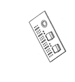
図1は、本発明による電気制御装置の部品の基本的構造を示す。本制御装置は、回路基板(1)、その上にはんだ付けされた半導体スイッチ(2)、カスタム形成されたバスバー(3)、熱伝導性絶縁箔(4)、そして例示的なヒートシンク(5)を含む。 FIG. 1 shows the basic structure of the components of an electric control device according to the invention. The controller includes a circuit board (1), a semiconductor switch (2) soldered thereon, a custom-formed bus bar (3), a thermally conductive insulating foil (4), and an exemplary heat sink (5). including.
本発明の第1の実施形態は、正面図として図2Aに、断面図として図2B〜2Dに示される。少なくとも一つのドリル孔(1.1)を有する回路基板(1)は、さらなる処理のための予備的固定が実現されるように、ピン状のスタンピング(3.1)を有する平坦なバスバーに接合される。バスバー(3)のピン(3.1)は、ピン(3.1)の上面が回路基板の上面(すなわち回路基板の銅層(1.2))に面合わせされるように回路基板(1)のドリル孔(1.1)に圧入される。バスバーは回路基板の底面に当接するが、全体の厚さが数ミリ増加するのみである。こうして形成された半組立部品は、さらに、通常の回路基板と全く同様に従来のSMD製造ラインで加工することができる。 The first embodiment of the present invention is shown in FIG. 2A as a front view and in FIGS. The circuit board (1) with at least one drill hole (1.1) is joined to a flat bus bar with pin-like stamping (3.1) so that a preliminary fixing for further processing is achieved Is done. The pin (3.1) of the bus bar (3) is formed on the circuit board (1) so that the upper surface of the pin (3.1) is flush with the upper surface of the circuit board (ie, the copper layer (1.2) of the circuit board). ) In the drill hole (1.1). The bus bar contacts the bottom surface of the circuit board, but the overall thickness only increases by a few millimeters. The semi-assembled part thus formed can be further processed on a conventional SMD production line in the same manner as a normal circuit board.
半導体スイッチは回路基板上に位置決めされ、他のSMD部品と一緒に回路基板にはんだ付けされることになる。半導体スイッチは、こうして回路基板の銅層(1.2)とピン(3.1)の上面との両方に当接する。これにより、半導体スイッチ(2.1)の底面とバスバー(3.2)のピンの上面との間に広範な接触がもたらされる。ここで、半導体スイッチ(2)、ピン(3.1)、回路基板(1)との間の空洞(6)は液状はんだで充填される。これにより、半導体スイッチとバスバー間の最適な熱的および電気的接続が実現される。 The semiconductor switch will be positioned on the circuit board and will be soldered to the circuit board along with other SMD components. The semiconductor switch thus contacts both the copper layer (1.2) of the circuit board and the top surface of the pin (3.1). This provides extensive contact between the bottom surface of the semiconductor switch (2.1) and the top surface of the pins of the bus bar (3.2). Here, the cavity (6) between the semiconductor switch (2), the pin (3.1), and the circuit board (1) is filled with liquid solder. Thereby, the optimal thermal and electrical connection between the semiconductor switch and the bus bar is realized.
このとき、ヒートシンク(5)は良好な熱的接続性を実現するために広い面積にわたってバスバー(3)に接続される。これは、例えば、接着または圧入により行うことができる。さらに、バスバー(3)とヒートシンク(5)の電気化学的分離(すなわち絶縁)は、熱輸送を損なわないようにできるだけ薄い絶縁箔(4)により簡単なやり方で実現することができる。絶縁箔は、また、接合機能を実現するためにも両面粘着性フィルムから成ってよい。組み立ての観点からは、バスバー(3)と回路基板(1)とを接合する前にヒートシンク(5)、絶縁箔(4)、そしてバスバー(3)を準備組み立て(preassembly)することも考えられる。あるいは、粘着性箔は、また、ヒートシンクまたはバスバーに適用される接着層で置換されてもよい。 At this time, the heat sink (5) is connected to the bus bar (3) over a wide area in order to realize good thermal connectivity. This can be done, for example, by gluing or press fitting. Furthermore, the electrochemical separation (i.e. insulation) of the bus bar (3) and the heat sink (5) can be realized in a simple manner with the insulating foil (4) as thin as possible so as not to impair the heat transport. The insulating foil may also be made of a double-sided adhesive film in order to realize a bonding function. From the viewpoint of assembly, it is also conceivable to pre-assemble the heat sink (5), the insulating foil (4), and the bus bar (3) before joining the bus bar (3) and the circuit board (1). Alternatively, the sticky foil may also be replaced with an adhesive layer applied to the heat sink or bus bar.
ヒートシンクは、好ましくは既成アルミニウムプロファイル部材から作られる。アルミニウムプロファイル部材の代わりに、金属ベースプレートの容器を使用してもよい。このとき、ベースプレートの内側は、バスバーと回路基板の両方が組立後にベースプレートにより支持されるように、バスバーを収容するための帯状の凹部を備えることができる。 The heat sink is preferably made from a prefabricated aluminum profile member. Instead of an aluminum profile member, a metal base plate container may be used. At this time, the inner side of the base plate can be provided with a band-shaped recess for receiving the bus bar so that both the bus bar and the circuit board are supported by the base plate after assembly.
図3Aには、ピン(3.1)を有する深絞り部品としてのバスバー(3)の構成を示す。深絞りにより、バスバー(3)の特に費用効果が高く精密な製造が可能となる。好ましくは、バスバーは、それ以上の加工工程を必要としない平坦で実質的に細長矩形状の金属板から製造される。この製造方法は、差込み可能な接触(3.3)をバスバー(3)の一端上に形成することにより、バスバー(3)へのおよびバスバー(3)からの(例えばケーブル内に)安全な電流供給を容易に実現する。あるいは、接続ピンまたはスレッドスタッドを、例えば、ケーブルとそれとを接続するためのバスバー内に圧入してもよい。好ましくは細長状の金属板から直接形成される圧着接続部などの他の接触手段もまた可能である。 FIG. 3A shows the configuration of the bus bar (3) as a deep drawing component having a pin (3.1). Deep drawing allows a particularly cost-effective and precise production of the bus bar (3). Preferably, the bus bar is manufactured from a flat, substantially elongated rectangular metal plate that does not require further processing steps. This manufacturing method provides a safe current to and from the bus bar (3) (eg in the cable) by forming a pluggable contact (3.3) on one end of the bus bar (3). Easy supply. Alternatively, the connection pin or thread stud may be press-fitted into a bus bar for connecting the cable and the cable, for example. Other contact means are also possible, such as a crimp connection, preferably formed directly from an elongated metal plate.
本発明の第2の実施形態は、正面図として図4Aに、断面図として図4B〜4Dに示される。バスバー(7)は、穿孔された平坦な細長状の金属板として形成される。細長状の金属板は平坦で基本的には矩形であることが好ましい。回路基板(1)内のドリル孔内に突出するピンは第1の実施形態のように細長状の金属板自体からは形成されず、個別の固体の円筒状構成要素(8)を細長状の金属板(7)(図3B参照)内に圧入することにより形成される。したがって、バスバーは特に簡単で費用効果が高いやり方で製造することができる。さらなる製造工程は上述したやり方で行なわれる。この構成は、バスバー(7)と半導体スイッチ(2)との間の熱的な結合が改良されるため有利である。 The second embodiment of the present invention is shown in FIG. 4A as a front view and in FIGS. The bus bar (7) is formed as a perforated flat elongated metal plate. The elongated metal plate is preferably flat and basically rectangular. The pin protruding into the drill hole in the circuit board (1) is not formed from the elongated metal plate itself as in the first embodiment, and the individual solid cylindrical component (8) is formed into an elongated shape. It is formed by press-fitting into a metal plate (7) (see FIG. 3B). The bus bar can therefore be manufactured in a particularly simple and cost-effective manner. Further manufacturing steps are performed in the manner described above. This configuration is advantageous because the thermal coupling between the bus bar (7) and the semiconductor switch (2) is improved.
この変形の代替として、ピン(8)を最初に圧入し、そして回路基板(1)(図3C参照)にはんだ付けすることも考えられる。この半組立部品により、バスバーとピン(8)は、例えば確動嵌合突起(8.1)を形成することによりドリル孔(7.1)により接合される。 As an alternative to this variant, it is also conceivable to first press-fit the pin (8) and solder it to the circuit board (1) (see FIG. 3C). With this semi-assembled part, the bus bar and the pin (8) are joined by a drill hole (7.1), for example, by forming a positive fitting protrusion (8.1).
一体化した熱伝導素子を備えたバスバー単体(すなわちヒートシンクなし)は、主として、差し込み可能接点を介し電流を供給すること、個々のパワー半導体に電流を分配すること、パワー半導体の熱を抽出すること、そして熱を拡散するにあたって熱を回路基板の反対側すなわちパワー半導体の反対側に運ぶこと、に関与する。熱を拡散させることは、パワー半導体から生ずる熱の流れの入力断面が、ヒートシンクに流れ込む熱伝導素子(バスバーの一部としての)における熱の流れの出力断面より小さいことを意味する。 A single bus bar with integrated heat transfer elements (ie without heat sink) mainly supplies current through pluggable contacts, distributes current to individual power semiconductors, extracts power semiconductor heat. And in transferring heat to the opposite side of the circuit board, ie the opposite side of the power semiconductor. Dissipating heat means that the input cross-section of the heat flow arising from the power semiconductor is smaller than the output cross-section of the heat flow in the heat conducting element (as part of the bus bar) that flows into the heat sink.
例えば周囲空気へのさらなる熱輸送と熱移動は個別のヒートシンクにより実現される。好ましくはできるだけ大きな表面を介しヒートシンクをバスバーに連結することにより、2つの部品を電気的に絶縁するための薄い絶縁箔がバスバーとヒートシンクとの間の熱輸送をわずかに劣化させるのみとなるように実現することができる。厚さdを有する絶縁箔が置かれた転送面Aが大きければ大きいほど、得られる絶縁箔の熱抵抗RthはRth〜d/Aの関係で小さくなる。 For example, further heat transport and heat transfer to the ambient air is realized by separate heat sinks. Preferably, by connecting the heat sink to the bus bar through as large a surface as possible, the thin insulating foil to electrically insulate the two components will only slightly degrade the heat transport between the bus bar and the heat sink. Can be realized. The greater the transfer surface A of the insulating foil is placed with a thickness d is greater, the thermal resistance R th of the resulting insulating foil is small in relation to R th to d / A.
したがって、一体化された熱伝導素子を備えたバスバーは、回路基板全体の良好な熱輸送を容易にする機能と、さらに、好ましくは電気的に絶縁されたヒートシンク内に余分な熱を結合する機能とを有する。 Thus, the busbar with integrated heat conducting elements has the function of facilitating good heat transport across the circuit board and, moreover, the function of coupling excess heat, preferably in an electrically insulated heat sink And have.
本発明による熱除去機能を有するバスバーのさらなる利点は、ヒートシンクと組み合わせたバスバーが半導体スイッチ間を熱的に結合することができることである。例えば破損を起因とする半導体スイッチの一つの過剰な発熱が存在する場合、他の半導体スイッチのスイッチを切ることによりヒートシンク全体を熱除去のために提供することができる。これにより、障害状況での制御ユニットのさらなる安全向上が可能となる。本発明は、もはやいくつかの個々の熱伝導素子を回路に取り付けその後バスバーに接続する必要がなく、これらの個々の部品は平坦な細長状の金属板を穿孔して形成することにより単一の製造工程で製造されるという意味で、製造と組立の際の大幅な単純化を実現する。同時に、この細長片の一端は、また、差し込み可能な接続のための刃形接触子として形成されてもよい。したがって、熱除去機能を有するバスバーは、3つの異なる機能、すなわち電流分配および供給、熱除去、そして差し込み可能接点の提供を担うことができる。 A further advantage of the bus bar having a heat removal function according to the present invention is that the bus bar combined with the heat sink can thermally couple between the semiconductor switches. For example, if there is excessive heat generation in one of the semiconductor switches due to damage, the entire heat sink can be provided for heat removal by switching off the other semiconductor switch. This makes it possible to further improve the safety of the control unit in a failure situation. The present invention no longer requires several individual heat conducting elements to be attached to the circuit and then connected to the bus bar, and these individual parts are formed by perforating and forming a flat elongated metal plate. Significant simplification during manufacturing and assembly in the sense that it is manufactured in the manufacturing process. At the same time, one end of the strip may also be formed as a blade contact for a pluggable connection. Thus, a bus bar with a heat removal function can be responsible for three different functions: current distribution and supply, heat removal, and provision of pluggable contacts.
本発明の一体化された熱伝導素子を備えたバスバーは、単一の組立および接続プロセスにおいて回路基板に機械的に嵌め込まれる。電気的および熱的な接続性ははんだ処理中に実現される。すなわち、バスバーが回路基板に機械的に固定された後、はんだペーストが一般的にはスクリーン印刷により回路基板に(そして突出する熱伝導素子に)塗布される。その後、パワー半導体と他の電子部品が装備される。次のリフロー工程では、熱伝導素子、パワー半導体および他の部品、そして回路基板は、同時に互いにはんだ付けされる。 The bus bar with integrated heat conducting elements of the present invention is mechanically fitted to the circuit board in a single assembly and connection process. Electrical and thermal connectivity is achieved during solder processing. That is, after the bus bar is mechanically fixed to the circuit board, the solder paste is applied to the circuit board (and to the protruding heat conduction element), generally by screen printing. After that, power semiconductors and other electronic components are installed. In the next reflow process, the heat conducting element, power semiconductor and other components, and the circuit board are simultaneously soldered together.
図5には、第2のバスバー(10)を有する構造を示す。このバスバーは第1のバスバー(3)と同じ構成を有することができ、半導体スイッチの電流供給と熱除去を行う。2つのバスバーを有するこの構成は、回路に高電流を供給しなければならずそして高電流が再び合流される前にいくつかの半導体スイッチに分配される状況において好ましくは使用される。これは、例えば、通電容量を増すために回路基板上のいくつかの半導体スイッチが並列に接続される場合に常にあてはまる。第2のバスバー(10)のピンも、また、回路基板内のドリル孔を貫通して上面上に突出するが、ここには半導体スイッチは一切はんだ付けされない。ピンを有するバスバーの、回路基板上の半導体スイッチまたは別の部品への電気的接続は、該ピンがはんだ付けされる回路基板上の銅領域により実現される。 FIG. 5 shows a structure having a second bus bar (10). This bus bar can have the same configuration as the first bus bar (3), and supplies current to the semiconductor switch and removes heat. This configuration with two bus bars is preferably used in situations where a high current must be supplied to the circuit and is distributed to several semiconductor switches before the high current is recombined. This is always the case, for example, when several semiconductor switches on the circuit board are connected in parallel to increase the current carrying capacity. The pins of the second bus bar (10) also pass through the drill holes in the circuit board and protrude above the upper surface, but here no semiconductor switch is soldered. The electrical connection of a bus bar with pins to a semiconductor switch or another component on the circuit board is achieved by a copper area on the circuit board to which the pins are soldered.
図6には、随意的なバスバーと回路基板の取り付けを示す。この目的を達成するために、熱伝導素子は、安全な準備組み立てを容易にするように回路基板内のドリル孔(13)と係合する隆起状の実装素子(12)を備える。これは、回路基板内のドリル孔への圧入嵌合がなされるように実装素子を大きめにすることで実現される。あるいは、少なくとも2つの実装素子(図6Cの12.1と12.2)は、回路基板との摩擦ロックを実現するためにプレテンション(F)下で設置されてよい。 FIG. 6 shows optional busbar and circuit board attachment. To achieve this objective, the heat conducting element comprises a raised mounting element (12) that engages a drill hole (13) in the circuit board to facilitate safe preparatory assembly. This is realized by enlarging the mounting element so as to be press-fitted into the drill hole in the circuit board. Alternatively, at least two mounting elements (12.1 and 12.2 in FIG. 6C) may be placed under pretension (F) to achieve a friction lock with the circuit board.
要約すると、本発明は、表面実装型半導体スイッチのための簡単でコスト的に有効な電流供給と熱除去を可能にする。この目的を達成するために、バスバーが使用される、すなわちバスバーは半導体スイッチと電気的および熱的に接触した熱伝導素子を介し使用される。半導体スイッチの動作中に発生した熱は、バスバー上に配置されたヒートシンクを介し除去される。バスバーは回路基板の底面に当接する簡単で平坦な素子である。したがって、バスバーと回路基板は、さらなる組立のために従来のSMD生産ラインを通すことができる半組立部品を形成する。 In summary, the present invention enables a simple and cost effective current supply and heat removal for surface mount semiconductor switches. To achieve this purpose, a bus bar is used, i.e. the bus bar is used via a heat conducting element in electrical and thermal contact with the semiconductor switch. Heat generated during operation of the semiconductor switch is removed through a heat sink disposed on the bus bar. The bus bar is a simple and flat element that contacts the bottom surface of the circuit board. The bus bar and circuit board thus form a semi-assembled part that can be passed through a conventional SMD production line for further assembly.
Claims (32)
前記回路基板(1)の上面上のパワー半導体部品(2)と、
前記回路基板(1)内の開口部を介し前記パワー半導体部品(2)と熱的に接触する熱伝導素子(3.1;8)と、
前記パワー半導体部品(2)の動作中に発生した熱を除去するために前記回路基板(1)の底面上に配置されたヒートシンク(5)と、を含む電気制御ユニットであって、
バスバー(3;7)が前記回路基板(1)の底面に平面的に当接するとともに前記熱伝導素子(3.1;8)と電気的および熱的に接触し、
前記熱伝導素子(3.1;8)は、前記パワー半導体部品(2)に電流を供給するとともにそれから電流を取り出すために前記回路基板(1)内の前記開口部を介し前記パワー半導体部品(2)と電気的に接触し、
前記ヒートシンク(5)は前記バスバー(3;7)上に配置されそれと熱的に接触する、ことを特徴とする電気制御ユニット。 A circuit board (1);
A power semiconductor component (2) on the upper surface of the circuit board (1);
A thermally conductive element (3.1; 8) in thermal contact with the power semiconductor component (2) through an opening in the circuit board (1);
A heat sink (5) disposed on the bottom surface of the circuit board (1) for removing heat generated during operation of the power semiconductor component (2),
A bus bar (3; 7) is in planar contact with the bottom surface of the circuit board (1) and is in electrical and thermal contact with the heat conducting element (3.1; 8);
The heat conducting element (3.1; 8) supplies the current to the power semiconductor component (2) and takes out the current from the power semiconductor component (2) through the opening in the circuit board (1). 2) in electrical contact with
Electric control unit, wherein the heat sink (5) is arranged on the bus bar (3; 7) and is in thermal contact therewith.
前記回路基板(1)内の開口部を介し前記パワー半導体部品(2)と熱的および電気的に接触する熱伝導素子(3.1;8)と、
前記回路基板(1)の底面に当接するとともに、前記熱伝導素子(3.1;8)と電気的および熱的に接触したバスバー(3;7)と、
前記パワー半導体部品(2)の動作中に発生した熱を除去するための前記バスバー(3;7)上に配置されたヒートシンク(5)と、を含む電気制御ユニットを製造する方法であって、
前記回路基板(1)を前記バスバー(3;7)上に予め機械的に固定することにより半組立部品を構築する工程であって、前記バスバー(3;7)は、前記ピンの上面が前記回路基板(1)の上面に面合わせされるように下から前記回路基板(1)の対応する開口部内に突出する少なくとも一つのピンを備える、工程と、
前記半組立部品の上面上にはんだペーストを塗布する工程と、
前記パワー半導体部品が前記回路基板(1)の上面と前記ピンの上面に当接するように前記半組立部品の上面上に前記パワー半導体部品を装備する工程と、
前記パワー半導体部品を前記回路基板(1)と前記ピンにはんだ付けする工程と、を含む方法。 A power semiconductor component (2) on the upper surface of the circuit board (1);
A thermally conductive element (3.1; 8) in thermal and electrical contact with the power semiconductor component (2) through an opening in the circuit board (1);
A bus bar (3; 7) in contact with the bottom surface of the circuit board (1) and in electrical and thermal contact with the heat conducting element (3.1; 8);
A heat sink (5) disposed on the bus bar (3; 7) for removing heat generated during operation of the power semiconductor component (2), comprising:
A step of constructing a semi-assembled part by mechanically fixing the circuit board (1) on the bus bar (3; 7) in advance, wherein the upper surface of the pin of the bus bar (3; 7) Comprising at least one pin projecting from below into the corresponding opening of the circuit board (1) so as to be flush with the upper surface of the circuit board (1);
Applying a solder paste on the upper surface of the semi-assembled part;
Mounting the power semiconductor component on the upper surface of the semi-assembled component such that the power semiconductor component contacts the upper surface of the circuit board (1) and the upper surface of the pin;
Soldering the power semiconductor component to the circuit board (1) and the pin.
A method according to claim 21 for producing a control unit according to any of claims 1 to 20.
Applications Claiming Priority (1)
| Application Number | Priority Date | Filing Date | Title |
|---|---|---|---|
| EP07019158A EP2043412B1 (en) | 2007-09-28 | 2007-09-28 | Conductor rail with heat conduction |
Publications (1)
| Publication Number | Publication Date |
|---|---|
| JP2009117805A true JP2009117805A (en) | 2009-05-28 |
Family
ID=38984589
Family Applications (1)
| Application Number | Title | Priority Date | Filing Date |
|---|---|---|---|
| JP2008242729A Withdrawn JP2009117805A (en) | 2007-09-28 | 2008-09-22 | Bus bar having heat removal function |
Country Status (6)
| Country | Link |
|---|---|
| EP (1) | EP2043412B1 (en) |
| JP (1) | JP2009117805A (en) |
| KR (1) | KR20090033015A (en) |
| CN (1) | CN101400246A (en) |
| DE (1) | DE502007003871D1 (en) |
| ES (1) | ES2345118T3 (en) |
Cited By (7)
| Publication number | Priority date | Publication date | Assignee | Title |
|---|---|---|---|---|
| JP2013135106A (en) * | 2011-12-27 | 2013-07-08 | Mitsubishi Electric Corp | Electric current aid member and electric current aid assembly using the same |
| JP2014533076A (en) * | 2011-10-31 | 2014-12-08 | フロニウス・インテルナツィオナール・ゲゼルシャフト・ミット・ベシュレンクテル・ハフツングFronius International Gmbh | Synchronous rectifier |
| JP2015046479A (en) * | 2013-08-28 | 2015-03-12 | 株式会社オートネットワーク技術研究所 | Circuit configuration |
| WO2015098499A1 (en) * | 2013-12-26 | 2015-07-02 | 株式会社 豊田自動織機 | Electronic apparatus |
| WO2020049975A1 (en) * | 2018-09-03 | 2020-03-12 | 株式会社オートネットワーク技術研究所 | Circuit structure and method for producing circuit structure |
| WO2021187156A1 (en) * | 2020-03-19 | 2021-09-23 | 株式会社オートネットワーク技術研究所 | Circuit structure |
| EP3822997A4 (en) * | 2018-06-05 | 2022-04-06 | Nippon Chemi-Con Corporation | Busbar laminate, electronic component mounting module including same, and method of manufacturing busbar laminate |
Families Citing this family (34)
| Publication number | Priority date | Publication date | Assignee | Title |
|---|---|---|---|---|
| US9151385B2 (en) | 2007-10-27 | 2015-10-06 | Continental Teves Ag & Co. Ohg | Multi-part piston construction for a brake caliper of a disk brake |
| DE102009005067A1 (en) * | 2009-01-19 | 2010-07-22 | Trw Automotive Gmbh | Plate for cover for locking housing of vehicle control unit, has one or multiple areas made from one material with heat conductivity and one or multiple other areas made from another material |
| DE102009010642A1 (en) * | 2009-02-26 | 2010-09-09 | Osram Gesellschaft mit beschränkter Haftung | Module for lighting applications, particularly light emitting diode driver module, for video projectors and projection device, has heat sink and electrically insulating film attached to heat sink |
| EP2323465B1 (en) | 2009-11-10 | 2013-02-20 | OSRAM GmbH | Electrical circuit with heat sink |
| WO2011113867A1 (en) * | 2010-03-18 | 2011-09-22 | Continental Automotive Gmbh | Circuit unit with a busbar for current and heat transmission and a method for producing said circuit unit |
| EP2675053A4 (en) | 2011-02-10 | 2015-01-07 | Mitsubishi Electric Corp | Power conversion device |
| DE102011102484B4 (en) | 2011-05-24 | 2020-03-05 | Jumatech Gmbh | Printed circuit board with molded part and process for its production |
| JP5440634B2 (en) * | 2012-03-15 | 2014-03-12 | 株式会社豊田自動織機 | Power converter |
| DE102012204133A1 (en) * | 2012-03-16 | 2013-09-19 | Continental Automotive Gmbh | Method, apparatus and system for a power circuit |
| EP2648283A1 (en) * | 2012-04-05 | 2013-10-09 | ABB Schweiz AG | Pole connector for electrically conductive connection of two neighbouring switch poles of a multi-pole low voltage circuit |
| DE102013212263A1 (en) | 2013-06-26 | 2014-12-31 | Robert Bosch Gmbh | Electrical circuit arrangement |
| DE102013113220B4 (en) | 2013-11-29 | 2022-01-05 | HELLA GmbH & Co. KGaA | Device for switching electrical currents and method for supplying electrical current |
| DE102014000126A1 (en) * | 2014-01-13 | 2015-07-16 | Auto-Kabel Management Gmbh | Printed circuit board, circuit and method for producing a circuit |
| DE102014006346A1 (en) * | 2014-04-30 | 2015-11-05 | Ellenberger & Poensgen Gmbh | High current switch |
| EP2966934B1 (en) | 2014-07-08 | 2016-09-14 | Eberspächer catem GmbH & Co. KG | Control device for an electric heating device and method for its production |
| DE102014218967B4 (en) * | 2014-09-22 | 2016-07-07 | Robert Bosch Gmbh | circuit board |
| DE102014219738A1 (en) * | 2014-09-30 | 2016-03-31 | Zf Friedrichshafen Ag | Busbar configuration |
| JP6256364B2 (en) * | 2015-02-03 | 2018-01-10 | 株式会社オートネットワーク技術研究所 | Circuit structure |
| CN105048721A (en) * | 2015-06-05 | 2015-11-11 | 上海法雷奥汽车电器系统有限公司 | Regulator for motor, and assembling method |
| DE102016101305B4 (en) | 2016-01-26 | 2017-11-16 | Eberspächer Controls Landau Gmbh & Co. Kg | Method of assembling a printed circuit board and printed circuit board assembly |
| CN106129024A (en) * | 2016-08-16 | 2016-11-16 | 中山大象动力科技有限公司 | A kind of power semiconductor device module based on heat dissipation design |
| GB2563186A (en) * | 2017-01-30 | 2018-12-12 | Yasa Motors Ltd | Semiconductor arrangement |
| GB2559180B (en) | 2017-01-30 | 2020-09-09 | Yasa Ltd | Semiconductor cooling arrangement |
| DE102017111944A1 (en) | 2017-05-31 | 2018-12-06 | Eberspächer Controls Landau Gmbh & Co. Kg | Electrical circuit unit and method for producing an electrical circuit unit |
| DE102018205243A1 (en) * | 2018-04-09 | 2019-10-10 | Zf Friedrichshafen Ag | Electronic power control module and method of manufacturing an electronic power control module |
| EP3562286A1 (en) | 2018-04-25 | 2019-10-30 | Siemens Aktiengesellschaft | Baking tray and method for its manufacture |
| CN112544127A (en) * | 2018-05-25 | 2021-03-23 | 米巴能源控股有限公司 | Power structure assembly with defined transfer path and method for manufacturing |
| US11495908B2 (en) * | 2019-04-01 | 2022-11-08 | Aptiv Technologies Limited | Electrical connector assembly with liquid cooling features |
| DE102020106492A1 (en) | 2019-04-12 | 2020-10-15 | Infineon Technologies Ag | CHIP PACKAGE, METHOD OF FORMING A CHIP PACKAGE, SEMICONDUCTOR DEVICE, SEMICONDUCTOR ARRANGEMENT, THREE-PHASE SYSTEM, METHOD FOR FORMING A SEMICONDUCTOR DEVICE, AND METHOD FOR FORMING A SEMICONDUCTOR ARRANGEMENT |
| DE102019122035A1 (en) * | 2019-08-16 | 2021-02-18 | Seg Automotive Germany Gmbh | Semiconductor component assembly and method of manufacturing therefor |
| CN110446333B (en) * | 2019-09-05 | 2021-10-22 | 浙江致威电子科技有限公司 | Bus sheet for printed circuit board and printed circuit board |
| US11539158B2 (en) | 2019-09-09 | 2022-12-27 | Aptiv Technologies Limited | Electrical terminal seal and electrical connector containing same |
| DE102020216305B4 (en) | 2020-12-18 | 2022-10-13 | Leoni Bordnetz-Systeme Gmbh | Electrical switching device |
| DE102022202817A1 (en) | 2022-03-23 | 2023-09-28 | Robert Bosch Gesellschaft mit beschränkter Haftung | Device for cooling at least one electrical component of a printed circuit board |
Citations (1)
| Publication number | Priority date | Publication date | Assignee | Title |
|---|---|---|---|---|
| JP2004031416A (en) * | 2002-06-21 | 2004-01-29 | Auto Network Gijutsu Kenkyusho:Kk | Power module |
Family Cites Families (3)
| Publication number | Priority date | Publication date | Assignee | Title |
|---|---|---|---|---|
| DE19518522C2 (en) * | 1995-05-19 | 1997-08-28 | Siemens Ag | Control device for a motor vehicle |
| SE510980C2 (en) * | 1996-11-29 | 1999-07-19 | Ericsson Telefon Ab L M | Device for mounting a capsule on a mounting base and method for manufacturing such a device |
| DE19935803A1 (en) * | 1998-08-04 | 2000-02-17 | Methode Electronics Inc | Semiconductor switching installation with integrated current bus has bottom side mechanically connected to heat dissipation device |
-
2007
- 2007-09-28 ES ES07019158T patent/ES2345118T3/en active Active
- 2007-09-28 DE DE502007003871T patent/DE502007003871D1/en active Active
- 2007-09-28 EP EP07019158A patent/EP2043412B1/en active Active
-
2008
- 2008-09-22 JP JP2008242729A patent/JP2009117805A/en not_active Withdrawn
- 2008-09-23 KR KR1020080092994A patent/KR20090033015A/en not_active Application Discontinuation
- 2008-09-26 CN CNA2008102114872A patent/CN101400246A/en active Pending
Patent Citations (1)
| Publication number | Priority date | Publication date | Assignee | Title |
|---|---|---|---|---|
| JP2004031416A (en) * | 2002-06-21 | 2004-01-29 | Auto Network Gijutsu Kenkyusho:Kk | Power module |
Cited By (12)
| Publication number | Priority date | Publication date | Assignee | Title |
|---|---|---|---|---|
| JP2014533076A (en) * | 2011-10-31 | 2014-12-08 | フロニウス・インテルナツィオナール・ゲゼルシャフト・ミット・ベシュレンクテル・ハフツングFronius International Gmbh | Synchronous rectifier |
| US9595882B2 (en) | 2011-10-31 | 2017-03-14 | Fronius International Gmbh | Synchronous rectifier |
| KR101782026B1 (en) * | 2011-10-31 | 2017-10-23 | 프로니우스 인터내셔널 게엠베하 | Synchronous rectifier |
| JP2013135106A (en) * | 2011-12-27 | 2013-07-08 | Mitsubishi Electric Corp | Electric current aid member and electric current aid assembly using the same |
| JP2015046479A (en) * | 2013-08-28 | 2015-03-12 | 株式会社オートネットワーク技術研究所 | Circuit configuration |
| WO2015098499A1 (en) * | 2013-12-26 | 2015-07-02 | 株式会社 豊田自動織機 | Electronic apparatus |
| JP2015126105A (en) * | 2013-12-26 | 2015-07-06 | 株式会社豊田自動織機 | Electronic device |
| EP3822997A4 (en) * | 2018-06-05 | 2022-04-06 | Nippon Chemi-Con Corporation | Busbar laminate, electronic component mounting module including same, and method of manufacturing busbar laminate |
| WO2020049975A1 (en) * | 2018-09-03 | 2020-03-12 | 株式会社オートネットワーク技術研究所 | Circuit structure and method for producing circuit structure |
| WO2021187156A1 (en) * | 2020-03-19 | 2021-09-23 | 株式会社オートネットワーク技術研究所 | Circuit structure |
| JP2021150498A (en) * | 2020-03-19 | 2021-09-27 | 株式会社オートネットワーク技術研究所 | Circuit structure |
| JP7419906B2 (en) | 2020-03-19 | 2024-01-23 | 株式会社オートネットワーク技術研究所 | circuit construct |
Also Published As
| Publication number | Publication date |
|---|---|
| KR20090033015A (en) | 2009-04-01 |
| EP2043412A1 (en) | 2009-04-01 |
| EP2043412B1 (en) | 2010-05-19 |
| CN101400246A (en) | 2009-04-01 |
| ES2345118T3 (en) | 2010-09-15 |
| DE502007003871D1 (en) | 2010-07-01 |
Similar Documents
| Publication | Publication Date | Title |
|---|---|---|
| JP2009117805A (en) | Bus bar having heat removal function | |
| US9041196B2 (en) | Semiconductor module arrangement and method for producing and operating a semiconductor module arrangement | |
| EP1638384A1 (en) | Circuit arrangement for cooling of surface mounted semi-conductors | |
| CN108370142B (en) | Circuit structure and electrical junction box | |
| WO2005076676A1 (en) | Circuit constituting body | |
| JP2003218562A (en) | Electric junction box | |
| WO2015170583A1 (en) | Circuit structure and electrical junction box | |
| JP2004253759A (en) | Control circuit board and circuit construct | |
| US7265983B2 (en) | Power unit comprising a heat sink, and assembly method | |
| JP2016152349A (en) | Circuit structure | |
| CN105830297A (en) | Circuit structure | |
| CN107112654B (en) | Module-terminal board connection structure and connection method | |
| US9991621B2 (en) | Optoelectronic arrangement | |
| US7688591B2 (en) | Electronic-component-mounting board | |
| JP2005268648A (en) | Circuit structure | |
| CN106256063B (en) | circuit structure and electric connection box | |
| JPH08274421A (en) | Electronic circuit unit | |
| CN112425018B (en) | Electrical junction box | |
| JP2010080795A (en) | Heat generating component mounted circuit board | |
| KR20180060572A (en) | Device package having heat dissipating member and the manufacturing method thereof | |
| US11349375B2 (en) | Electric machine with a heat transfer device for transferring heat from an electronic component to a heat sink | |
| GB2296604A (en) | Electric device | |
| JP2020038883A (en) | Circuit structure and method of manufacturing circuit structure | |
| US20030171026A1 (en) | Electrical device | |
| JPWO2017209168A1 (en) | Electric wire connection structure of metal core printed circuit board, metal core printed circuit board and manufacturing method thereof |
Legal Events
| Date | Code | Title | Description |
|---|---|---|---|
| A761 | Written withdrawal of application |
Free format text: JAPANESE INTERMEDIATE CODE: A761 Effective date: 20090304 |
|
| A521 | Written amendment |
Free format text: JAPANESE INTERMEDIATE CODE: A821 Effective date: 20090304 |
|
| A977 | Report on retrieval |
Free format text: JAPANESE INTERMEDIATE CODE: A971007 Effective date: 20110629 |
|
| A131 | Notification of reasons for refusal |
Free format text: JAPANESE INTERMEDIATE CODE: A131 Effective date: 20110705 |
|
| A02 | Decision of refusal |
Free format text: JAPANESE INTERMEDIATE CODE: A02 Effective date: 20111206 |