JP2009111642A - Fine concave forming method and method for manufacturing condenser microphone - Google Patents
Fine concave forming method and method for manufacturing condenser microphone Download PDFInfo
- Publication number
- JP2009111642A JP2009111642A JP2007280866A JP2007280866A JP2009111642A JP 2009111642 A JP2009111642 A JP 2009111642A JP 2007280866 A JP2007280866 A JP 2007280866A JP 2007280866 A JP2007280866 A JP 2007280866A JP 2009111642 A JP2009111642 A JP 2009111642A
- Authority
- JP
- Japan
- Prior art keywords
- diaphragm
- plate
- film
- etching
- substrate
- Prior art date
- Legal status (The legal status is an assumption and is not a legal conclusion. Google has not performed a legal analysis and makes no representation as to the accuracy of the status listed.)
- Pending
Links
Images


Landscapes
- Micromachines (AREA)
- Electrostatic, Electromagnetic, Magneto- Strictive, And Variable-Resistance Transducers (AREA)
Abstract
Description
本発明は微細凹部形成方法およびコンデンサマイクロホンの製造方法に関し、特に単結晶ケイ素基板に微細な凹部を形成する方法に関する。 The present invention relates to a method for forming a fine recess and a method for manufacturing a condenser microphone, and more particularly to a method for forming a fine recess in a single crystal silicon substrate.
SF6等のガスによるエッチングとC4F8等のデポジションによる側壁保護とを繰り返すことによりケイ素基板に深い凹部を形成する技術が知られている。この技術は一般にボッシュプロセスといわれ、MEMS(Micro Electro Mechanical Systems)のプロセス技術として広く用いられている。 A technique is known in which a deep recess is formed in a silicon substrate by repeating etching with a gas such as SF 6 and side wall protection by deposition with C 4 F 8 or the like. This technique is generally called a Bosch process and is widely used as a process technique for MEMS (Micro Electro Mechanical Systems).
しかし、ボッシュプロセスでは等法的なエッチングを繰り返すことにより凹部の側壁に微小な凹凸が形成される。プロセス条件によってはこの凹凸に不規則な髭状の部分が生じたり、凹凸の突端部が脆い形態で形成され、これらの部分が残渣として脱落するという問題がある。ケイ素基板から脱落した残渣がMEMSの可動部に混入すると、MEMSの機能が損なわれる。特にコンデンサマイクロホンでは平行平板コンデンサを形成するダイヤフラムとプレートの間の間隙が狭く広いため、残渣の残存は信頼性を著しく低下させる。 However, in the Bosch process, minute etching is formed on the side wall of the recess by repeating isotropic etching. Depending on the process conditions, there is a problem that irregular ridges are formed on the irregularities, or the protruding ends of the irregularities are formed in a brittle form, and these parts fall off as residues. If the residue dropped from the silicon substrate is mixed into the movable part of the MEMS, the function of the MEMS is impaired. In particular, in a condenser microphone, since the gap between the diaphragm and the plate forming the parallel plate capacitor is narrow and wide, the remaining residue significantly reduces the reliability.
本発明はこの問題を解決するために創作されたものであって、ケイ素基板に残渣のない凹部を形成し、コンデンサマイクロホンの信頼性を高めることを目的とする。 The present invention has been created to solve this problem, and has an object to form a recess having no residue on a silicon substrate and to improve the reliability of a condenser microphone.
(1)上記目的を達成するための微細凹部形成方法は、エッチングと側壁保護膜の形成とを交互に繰り返してケイ素基板に凹部を形成し、前記側壁保護膜を除去して前記凹部の側壁を露出させ、露出した前記側壁の表層をエッチングにより除去する、ことを含む。
ケイ素基板に凹部を形成するために用いた側壁保護膜を除去して凹部の側壁を露出させた後に、露出した側壁の表層をエッチングにより除去すると、凹部の側壁に形成された微小な凹凸の髭状の部分や微小な凹凸の脆い突端部を消滅させることができる。したがって本発明によるとケイ素基板に残渣のない凹部を形成することができる。
(1) A method of forming a fine recess to achieve the above object is to form a recess in a silicon substrate by alternately repeating etching and formation of a sidewall protective film, and remove the sidewall protective film to form a sidewall of the recess. Exposing and removing the exposed surface layer of the sidewall by etching.
After removing the sidewall protective film used to form the recesses in the silicon substrate to expose the sidewalls of the recesses, the surface layer of the exposed sidewalls is removed by etching to remove minute irregularities formed on the sidewalls of the recesses. It is possible to eliminate the shape-like portion and the brittle tip portion of minute unevenness. Therefore, according to the present invention, a recess having no residue can be formed in the silicon substrate.
(2)上記目的を達成するための微細凹部形成方法において、露出した前記側壁の表層をアルカリ性溶液を用いたエッチングにより除去することが望ましい。 (2) In the method for forming fine recesses for achieving the above object, it is desirable to remove the exposed surface layer of the side wall by etching using an alkaline solution.
(3)テトラメチルアンモニウムハイドロオキサイド(TMAH)水溶液は単結晶ケイ素基板を結晶異方的にウェットエッチングするエッチャントとして好適であるが、酸化ケイ素に対するケイ素のエッチング選択比が非常に大きい。しかし、側壁保護膜が除去されたケイ素基板の凹部の側壁の表層には自然酸化膜が形成される。
したがって、前記側壁保護膜を除去した後に露出した前記側壁の表層を除去する前に、露出した前記側壁の表層に形成された自然酸化膜を除去し、前記自然酸化膜が除去された前記側壁の表層をテトラメチルアンモニウムハイドロオキサイド水溶液を用いたエッチングにより除去することが望ましい。
(3) Tetramethylammonium hydroxide (TMAH) aqueous solution is suitable as an etchant for anisotropically wet etching a single crystal silicon substrate, but has a very high etching selectivity ratio of silicon to silicon oxide. However, a natural oxide film is formed on the surface layer of the side wall of the recess of the silicon substrate from which the side wall protective film has been removed.
Therefore, before removing the exposed surface layer of the sidewall after removing the sidewall protective film, the exposed native oxide film formed on the exposed surface layer of the sidewall is removed, and the sidewall of the sidewall from which the natural oxide film has been removed is removed. It is desirable to remove the surface layer by etching using an aqueous tetramethylammonium hydroxide solution.
(4)上記目的を達成するためのコンデンサマイクロホンの製造方法は、エッチングと側壁保護膜の形成とを交互に繰り返すことにより、ダイヤフラムのバックキャビティとなる通孔を、エッチングストッパとなる酸化ケイ素膜が形成されたケイ素基板に形成し、前記側壁保護膜を除去して前記通孔の側壁を露出させ、露出した前記側壁の表層に形成された自然酸化膜を除去し、前記自然酸化膜が除去された前記側壁の表層をテトラメチルアンモニウムハイドロオキサイド水溶液を用いたエッチングにより除去する、ことを含む。
コンデンサマイクロホンにはダイヤフラムのバックキャビティが必要である。バックキャビティの容積はダイヤフラムの面積に対して十分大きいことが好ましい。そこで、本発明によると、ケイ素基板に通孔を形成し、この通孔がバックキャビティの少なくとも一部として用いられる。本発明では、エッチングと側壁保護膜の形成とを交互に繰り返すことによりケイ素基板に通孔を形成するとき、酸化ケイ素膜がエッチングストッパとして用いられる。側壁保護膜が除去されると凹部の側壁に自然酸化膜が形成される。本発明では、凹部の側壁に形成された微小な凹凸の髭状の部分や微小な凹凸の脆い突端部を、TMAH水溶液を用いて溶解し消滅させる。TMAH水溶液のケイ素の酸化ケイ素に対するエッチング選択比は非常に大きい。そこで本発明では、凹部の側壁の表層をTMAH水溶液で除去する前に側壁の表層に形成されている自然酸化膜を除去する。本発明では、このような一連のプロセスを実施することによって、ダイヤフラムのバックキャビティから残渣が脱落し、脱落した残渣によって生ずる不具合を防止できる。すなわち本発明によるとコンデンサマイクロホンの信頼性を高めることができる。
(4) A condenser microphone manufacturing method for achieving the above-described object is achieved by alternately repeating etching and forming a sidewall protective film so that a through-hole serving as a back cavity of the diaphragm becomes a silicon oxide film serving as an etching stopper. Formed on the formed silicon substrate, the sidewall protective film is removed to expose the sidewall of the through hole, the natural oxide film formed on the exposed surface layer of the sidewall is removed, and the natural oxide film is removed And removing the surface layer of the side wall by etching using an aqueous tetramethylammonium hydroxide solution.
Condenser microphones require a diaphragm back cavity. The volume of the back cavity is preferably sufficiently large with respect to the area of the diaphragm. Therefore, according to the present invention, a through hole is formed in the silicon substrate, and this through hole is used as at least a part of the back cavity. In the present invention, when the through hole is formed in the silicon substrate by alternately repeating the etching and the formation of the sidewall protective film, the silicon oxide film is used as an etching stopper. When the sidewall protective film is removed, a natural oxide film is formed on the sidewall of the recess. In the present invention, the minute concave and convex ridge-shaped portions formed on the side walls of the concave portions and the brittle tip portions of the minute concave and convex portions are dissolved and disappeared using the TMAH aqueous solution. The etching selectivity of silicon to silicon oxide in the TMAH aqueous solution is very large. Therefore, in the present invention, the natural oxide film formed on the surface layer of the side wall is removed before removing the surface layer on the side wall of the recess with the TMAH aqueous solution. In the present invention, by carrying out such a series of processes, the residue is dropped from the back cavity of the diaphragm, and a problem caused by the dropped residue can be prevented. That is, according to the present invention, the reliability of the condenser microphone can be improved.
以下、本発明の実施の形態を添付図面を参照しながら説明する。尚、各図において対応する構成要素には同一の符号が付され、重複する説明は省略される。 Hereinafter, embodiments of the present invention will be described with reference to the accompanying drawings. In addition, the same code | symbol is attached | subjected to the corresponding component in each figure, and the overlapping description is abbreviate | omitted.
1.構成
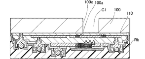
図1は本発明の一実施形態であるコンデンサマイクロホン1のMEMS構造部であるセンサチップを示し、図2はその模式的な断面を示し、図3はその膜の積層構造を示している。図18および図19はその一部の詳細な断面を示している。コンデンサマイクロホン1はセンサチップと、電源回路および増幅回路を備えた図示しない回路チップと、これらを収容する図示しないパッケージとから構成される。
1. Configuration FIG. 1 shows a sensor chip which is a MEMS structure part of a condenser microphone 1 according to an embodiment of the present invention, FIG. 2 shows a schematic cross section thereof, and FIG. 3 shows a laminated structure of the film. 18 and 19 show a detailed cross section of a part thereof. The condenser microphone 1 includes a sensor chip, a circuit chip (not shown) provided with a power supply circuit and an amplifier circuit, and a package (not shown) that accommodates these.
コンデンサマイクロホン1のセンサチップは、基板100と、その上に積層された下層絶縁膜110、下層導電膜120、上層絶縁膜130、上層導電膜160、表層絶縁膜170などの堆積膜とからなるチップである。尚、図1において上層導電膜160より上の層は示されていない。はじめにコンデンサマイクロホン1のMEMS構造部の膜の積層構造について説明する。
The sensor chip of the capacitor microphone 1 is a chip composed of a
基板100はP型単結晶ケイ素からなる。基板の材質はこれに限らず、薄膜を堆積するための下地基板および薄膜からなる構造体を支持する支持基板としての剛性、厚さ、靱性を備えていればよい。基板100には通孔が形成されており、その通孔の開口100aはバックキャビティC1の開口を形成している。
The
基板100、下層導電膜120および上層絶縁膜130に接合されている下層絶縁膜110は酸化ケイ素(SiOx)からなる堆積膜である。下層絶縁膜110は円周上に等間隔に配列された複数のダイヤフラム支持部102と、ダイヤフラム支持部102よりも内側において円周上に等間隔に配列された複数のガード絶縁部103と、ガードリング125cおよびガードリード125dを基板100から絶縁している環状の環状部101とを構成している。
The lower
下層絶縁膜110および上層絶縁膜130に接合されている下層導電膜120はPなどの不純物が全体にドーピングされた多結晶ケイ素からなる堆積膜である。下層導電膜120はガード電極125aとガードコネクタ125bとガードリング125cとガードリード125dとからなるガード部127と、ダイヤフラム123とを構成している。
The lower
下層導電膜120と上層導電膜160と下層絶縁膜110とに接合されている上層絶縁膜130は酸化ケイ素からなる堆積膜である。上層絶縁膜130は円周上に配列された複数のプレート支持部131とプレート支持部131の外側に位置しエッチストッパリング161を支持しプレートリード162dとガードリード125dとを絶縁する環状の環状部132とを構成している。
The upper
上層絶縁膜130に接合されている上層導電膜160はP等の不純物が全体にドーピングされた多結晶ケイ素からなる堆積膜である。上層導電膜160はプレート162と、プレートリード162dと、エッチストッパリング161とを構成している。
The upper
上層導電膜160および上層絶縁膜130に接合されている表層絶縁膜170は酸化ケイ素膜からなる絶縁性の堆積膜である。
A
コンデンサマイクロホン1のMEMS構造部には4つの端子125e、162e、123e、100bが設けられている。これらの端子125e、162e、123e、100bはAlSiなどの導電性の堆積膜であるパッド導電膜180、Niなどの導電性の堆積膜であるバンプ膜210、Auなどの耐腐食性に優れた導電性の堆積膜であるバンプ保護膜220とからなる。端子125e、162e、123e、100bはそれぞれSiNなどの絶縁性の堆積膜であるパッド保護膜190と酸化ケイ素などの絶縁性の堆積膜である表層保護膜200とによって側壁が保護されている。
The MEMS structure portion of the condenser microphone 1 is provided with four
以上、コンデンサマイクロホン1のMEMS構造部の膜の積層構造について説明した。次にコンデンサマイクロホン1のMEMS構造部の機械構造について説明する。 In the above, the laminated structure of the film | membrane of the MEMS structure part of the capacitor | condenser microphone 1 was demonstrated. Next, the mechanical structure of the MEMS structure part of the condenser microphone 1 will be described.
ダイヤフラム123は全体が導電性を有する単層の薄い堆積膜からなり、中央部123aと、中央部123aから外側に放射状に伸びる複数の腕部123cとを備える。ダイヤフラム123はその外縁近傍の複数箇所に接合されている複数の柱形のダイヤフラム支持部102によってプレート162との間と基板100との間とにそれぞれ空隙を挟んでプレート162から絶縁して支持され、基板100と平行に張り渡されている。ダイヤフラム支持部102は、ダイヤフラム123のそれぞれの腕部123cの先端部近傍に接合されている。ダイヤフラム123は腕部123cと腕部123cとの間が切り欠かれているため、切り欠きのない形態に比べて剛性が低くなっている。さらにそれぞれの腕部123cには通孔であるダイヤフラム孔123bが複数形成されているため、腕部123c自体の剛性も低くなっている。中央部123aの近傍において、ダイヤフラム123の腕部123cは中央部123aに接近するほどダイヤフラム123の周方向に長くなっている。これにより腕部123cと中央部123aとの境界における応力集中を緩和できる。また腕部123cと中央部123aとの境界近傍において腕部123cの輪郭に屈曲部を形成しないことにより屈曲部において応力集中が起こることを防止できる。
The
複数のダイヤフラム支持部102はバックキャビティC1の開口100aの周囲において開口100aの周方向に等間隔に配列されている。それぞれのダイヤフラム支持部102は絶縁性の堆積膜からなり柱形である。ダイヤフラム123は、その中央部123aがバックキャビティC1の開口100aを覆うように、これらのダイヤフラム支持部102によって基板100の上に支持されている。基板100とダイヤフラム123との間にはダイヤフラム支持部102の厚さに相当する空隙C2が形成されている。空隙C2はバックキャビティC1の気圧を大気圧と平衡させるために必要である。空隙C2はダイヤフラム123を振動させる音波がバックキャビティの開口100aに至るまでの経路における最大の音響抵抗を形成するように、低く、ダイヤフラム123の径方向の長さが長く形成されている。
The plurality of
ダイヤフラム123の基板100と対抗する面には複数のダイヤフラムバンプ123fが形成されている。このダイヤフラムバンプ123fはダイヤフラム123が基板100に付着(スティッキング)することを防止するための突起物であり、ダイヤフラム123を構成する下層導電膜120のうねりによって形成されている。すなわちダイヤフラムバンプ123fの裏側にはディンプル(凹み)が形成されている。
A plurality of diaphragm bumps 123 f are formed on the surface of the
ダイヤフラム123は複数の腕部123cのうちの1つの先端から伸びるダイヤフラムリード123dによってダイヤフラム端子123eに接続されている。ダイヤフラムリード123dは腕部123cより幅が狭くダイヤフラム123と同じ下層導電膜120によって構成されている。ダイヤフラムリード123dは環状のガードリング125cが分断されている領域を通ってダイヤフラム端子123eまで伸びている。ダイヤフラム端子123eと基板端子100bとは図示しない回路チップにおいて短絡しているため(図4参照)、ダイヤフラム123と基板100とは同電位である。
なお、ダイヤフラム123と基板100の電位が異なる場合にはダイヤフラム123と基板100とが寄生容量を形成するが、この場合であっても、ダイヤフラム123が複数のダイヤフラム支持部102によって支持されており、隣り合うダイヤフラム支持部102の間には空気層が存在するため、ダイヤフラム123が環状の壁構造のスペーサで支持される構造に比べると寄生容量が小さくなる。
The
When the potentials of the
プレート162は全体が導電性を有する単層の薄い堆積膜からなり、中央部162bと、中央部162bから外側に放射状に伸びる腕部162aとを備える。プレート162はその外縁近傍の複数箇所に接合されている複数の柱形のプレート支持部131に支持されている。またプレート162はその中心がダイヤフラム123の中心と重なるようにダイヤフラム123と平行に張り渡されている。プレート162の中心(中央部162bの中心)から中央部162bの外縁までの距離すなわちプレート162の中心から外縁までの最短距離は、ダイヤフラム123の中心(中央部123aの中心)から中央部123aの外縁までの距離すなわちダイヤフラム123の中心から外縁までの最短距離よりも短い。したがって振幅が小さいダイヤフラム123の外縁近傍領域において、プレート162はダイヤフラム123に対向しない。またプレート162の腕部162aと腕部162aとの間には切り欠きが形成されているため、ダイヤフラム123の外縁近傍に相当するプレート162の切り欠きの領域においてもプレート162とダイヤフラム123とが対向しない。そしてプレート162の切り欠きの領域にダイヤフラム123の腕部123cが伸びている。このため寄生容量を増大させることなくダイヤフラム123の振動の両端の間の距離、すなわちダイヤフラム123が張り渡される距離を長くとることができる。
The
プレート162には通孔であるプレート孔162cが複数形成されている。プレート孔162cはダイヤフラム123に音波を伝搬させる通路として機能するとともに、上層絶縁膜130を等方的にエッチングするためのエッチャントを通す孔としても機能する。上層絶縁膜130がエッチングされた後に残る部分がプレート支持部131および環状部132となりエッチングによって除去される部分がダイヤフラム123とプレート162との間の空隙C3となる。すなわちプレート孔162cは空隙C3とプレート支持部131とを同時に形成できるようにエッチャントを上層絶縁膜130に到達させるための通孔である。したがってプレート孔162cは空隙C3の高さやプレート支持部131の形状やエッチング速度に応じて配置されている。具体的にはプレート孔162cはプレート支持部131との接合領域とその周辺をのぞく中央部162bおよび腕部162aのほぼ全域にわたってほぼ等間隔に配列されている。隣り合うプレート孔162cの間隔を狭めるほど上層絶縁膜130の環状部132の幅を狭くしてチップの面積を狭くできる。一方、隣り合うプレート孔162cの間隔を狭めるほどプレート162の剛性が低くなる。
A plurality of plate holes 162 c that are through holes are formed in the
プレート支持部131はダイヤフラム123と同じ層に位置するガード電極125aに接合されている(ガード電極125aはダイヤフラム123と同じ下層導電膜120からなる。)。プレート支持部131はプレート162に接合されている絶縁性の堆積膜である上層絶縁膜130からなる。複数のプレート支持部131はバックキャビティC1の開口100aの周囲に等間隔に配列されている。それぞれのプレート支持部131はダイヤフラム123の腕部123cと腕部123cとの間の切り欠きの領域に位置するため、ダイヤフラム123の最大径よりも、プレート162の最大径を小さくすることができる。これによりプレート162の剛性が上がるとともにプレート162と基板100との寄生容量が小さくなる。
The
プレート162はそれぞれがガード絶縁部103とガード電極125aとプレート支持部131とによって構成される柱形の複数の構造体129によって基板100上に支持されている。構造体129によって、プレート162とダイヤフラム123との間には空隙C3が形成され、プレート162と基板100との間には空隙C3と空隙C2とが形成されている。ガード絶縁部103とプレート支持部131とが絶縁性を有するためプレート162は基板100から絶縁されている。
The
ガード電極125aがなく、プレート162の電位と基板100の電位とが異なる場合、プレート162と基板100とが対向している領域には寄生容量が生じ、特にこれらの間に絶縁物がある場合には寄生容量が大きくなる(図4A参照)。本実施形態ではプレート162を基板100上に支持するガード絶縁部103とガード電極125aとプレート支持部131とを1つの構造体としてとらえた構造体129が柱形であり、互いに離間した複数の構造体でプレート162を基板100上に支持する構造であるため、ガード電極125aがないとしても、環状の壁構造の絶縁物でプレート162が基板100上に支持される構造に比べると寄生容量が小さくなる。
When the
プレート162のダイヤフラム123と対向する面には複数の突起(プレートバンプ)162fが設けられている。プレートバンプ162fはプレート162を構成する上層導電膜160に接合された窒化ケイ素(SiN)膜と、窒化ケイ素膜に接合された多結晶ケイ素膜とからなる。プレートバンプ162fはダイヤフラム123がプレート162に付着(スティッキング)することを防止する。
A plurality of protrusions (plate bumps) 162 f are provided on the surface of the
プレート162の腕部162aの先端からは腕部162aより細いプレートリード162dがプレート端子162eまで伸びている。プレートリード162dはプレート162と同じ上層導電膜160からなる。プレートリード162dの配線経路はガードリード125dの配線経路と重なっている。このためプレートリード162dと基板100との寄生容量が低減される。
以上、コンデンサマイクロホン1のMEMS構造部の機械構造について説明した。
A
The mechanical structure of the MEMS structure part of the condenser microphone 1 has been described above.
2.作用
図4は回路チップとセンサチップとが接続されることにより構成される回路を示している。ダイヤフラム123には回路チップに備わるチャージポンプCPによって安定したバイアス電圧が印加される。このバイアス電圧が高いほど感度が高くなるがダイヤフラム123とプレート162とのスティクションが起きやすくなるためプレート162の剛性は重要である。
2. FIG. 4 shows a circuit configured by connecting a circuit chip and a sensor chip. A stable bias voltage is applied to the
図示しないパッケージの通孔から伝わる音波はプレート孔162cとプレート162の腕部間の切り欠き領域とを通ってダイヤフラム123に伝わる。プレート162には両面から同位相の音波が伝わるためプレート162は実質的に振動しない。ダイヤフラム123に伝わった音波はプレート162に対してダイヤフラム123を振動させる。ダイヤフラム123が振動するとプレート162とダイヤフラム123とを対向電極とする平行平板コンデンサの静電容量が変動する。この静電容量の変動は電圧信号として回路チップのアンプAに入力されて増幅される。センサチップの出力はハイインピーダンスであるためアンプAがパッケージ内に必要である。
A sound wave transmitted from a through hole of the package (not shown) is transmitted to the
基板100とダイヤフラム123とが短絡されているため、図3Aに示すようにガード部127のガード電極125aが存在しなければ相対的に振動しないプレート162と基板100とによって寄生容量が形成される。図3Bに示すようにアンプAの出力端をガード部127に接続し、アンプAによってボルテージフォロア回路を構成することによりプレート162と基板100とによって寄生容量が形成されないようになる。すなわちプレート162の腕部162aと基板100とが対向する領域において腕部162aと基板100との間にガード電極125aを設けることにより、プレート162の腕部162aと基板100とが対向する領域における寄生容量を低減できる。さらに、プレート162から伸びるプレートリード162dと対向する領域には、ガード電極同士を接続するガードリング125cからガード端子125eに伸びるガードリード125dが配線されているため、プレートリード162dと基板100とによっても寄生容量が形成されない。環状のガードリング125cはダイヤフラム123の周囲においてほぼ最短経路で複数のガード電極125aを接続している。またプレート162の周方向においてガード電極125aをプレート162の腕部162aより長く形成することによりさらに寄生容量が低減される。
Since the
なお、チャージポンプCP、アンプAなどの回路チップに備わる要素をセンサチップ内に設け、1チップ構造のコンデンサマイクロホン1を構成することも可能である。 Note that it is also possible to configure the one-chip capacitor microphone 1 by providing elements provided in the circuit chip such as the charge pump CP and the amplifier A in the sensor chip.
3.製造方法
次に図5から図17に基づいてコンデンサマイクロホン1の製造方法を説明する。
3. Manufacturing Method Next, a manufacturing method of the condenser microphone 1 will be described with reference to FIGS.
図5に示す工程では、まず基板100の表面全体に酸化ケイ素からなる下層絶縁膜110を形成する。下層絶縁膜110は、基板100に通孔を形成する工程におけるエッチングストッパとして機能し、ダイヤフラム123を振動させる音波がバックキャビティの開口100aに至るまでの経路における最大の音響抵抗を形成する空隙C2(図2参照)の高さに相当し、ダイヤフラムバンプ123fを形成するための犠牲層としても機能する。したがって下層絶縁膜110の厚さはこれらの機能を勘案して設定され、例えば1〜1.5μmとする。次に、ダイヤフラムバンプ123fを形成するためのディンプル110aをフォトレジストマスクを用いたエッチングにより下層絶縁膜110に形成する。次に、下層絶縁膜110の表面上にCVD法などを用いて多結晶ケイ素からなる下層導電膜120を形成する。すると、ディンプル110aの上にダイヤフラムバンプ123fが形成される。最後に、フォトレジストマスクを用いて下層導電膜120をエッチングすることにより、下層導電膜120からなるダイヤフラム123およびガード部127を形成する。
In the step shown in FIG. 5, first, a lower insulating
続いて図6に示す工程では、下層絶縁膜110と下層導電膜120の表面全体に酸化ケイ素からなる上層絶縁膜130を形成する。次に、プレートバンプ162fを形成するためのディンプル130aを、フォトレジストマスクを用いたエッチングにより上層絶縁膜130に形成する。
Subsequently, in the process shown in FIG. 6, an upper
続く図7に示す工程では、上層絶縁膜130の表面上に多結晶ケイ素膜135と窒化ケイ素膜136とからなるプレートバンプ162fを形成する。多結晶ケイ素膜135を周知の方法でパターニングした後に窒化ケイ素膜136が形成されるため、ディンプル130aから突出している多結晶ケイ素膜135の露出面全体が窒化ケイ素膜136で覆われる。窒化ケイ素膜136はスティッキング時にダイヤフラム123とプレート162とが短絡することを防止する絶縁膜である。
In the subsequent step shown in FIG. 7, a
続いて図8に示す工程では、上層絶縁膜130の露出面と窒化ケイ素膜136の表面にCVD法などを用いて多結晶ケイ素からなる上層導電膜160を形成する。次にフォトレジストマスクを用いて上層導電膜160をエッチングすることによりプレート162とプレートリード162dとエッチストッパリング161とを形成する。なおこの工程ではプレート孔162cは形成されない。
8, an upper
続いて図9に示す工程では、上層絶縁膜130にコンタクトホールCH1、CH3、CH4が形成され、続いて酸化ケイ素からなる表層絶縁膜170が表面全体に形成される。さらにフォトレジストマスクを用いたエッチングにより、表層絶縁膜170にコンタクトホールCH2を形成すると同時に表層絶縁膜170のコンタクトホールCH1、CH3、CH4の底部に形成されている部分を除去する。次にコンタクトホールCH1、CH2、CH3、CH4のそれぞれを埋めるAlSiからなるパッド導電膜180が形成され、コンタクトホールCH1、CH2、CH3、CH4を覆う部分を残して周知の方法でパターニングされる。さらに窒化ケイ素からなるパッド保護膜190が表層絶縁膜170およびパッド導電膜180の上にCVD法により形成されパット導電膜180の周囲にのみを残るようにパッド導電膜190が周知の方法によりパターニングされる。
Subsequently, in the step shown in FIG. 9, contact holes CH1, CH3, and CH4 are formed in the upper insulating
続いて図10に示す工程では、フォトレジストマスクを用いた異方性エッチングにより、プレート孔162cに対応する通孔170aが表層絶縁膜170に形成され、上層導電膜160にはプレート孔162cが形成される。この工程は連続的に実施され、通孔170aが形成された表層絶縁膜170は上層導電膜160のレジストマスクとして機能する。
Subsequently, in the step shown in FIG. 10, through
続いて図11に示す工程では、酸化ケイ素からなる表層保護膜200が表層絶縁膜170とパッド保護膜190の表面に形成される。このとき表層絶縁膜170の通孔170aとプレート孔162cとは表層保護膜200によって埋められる。
Subsequently, in the step shown in FIG. 11, a surface
続いて図12に示す工程では、コンタクトホールCH1、CH2、CH3、CH4にそれぞれ形成されているパッド導電膜180の表面にNiからなるバンプ膜210を形成し、バンプ膜210の表面にAuからなるバンプ保護膜220を形成する。さらにこの段階で基板100の裏面を研削し、基板100の厚さを完成寸法である525μmにする。
Subsequently, in the step shown in FIG. 12, a
続いて図13に示す工程では、フォトレジストマスクを用いたエッチングにより、表層保護膜200と表層絶縁膜170とにエッチストッパリング161が露出する通孔H5を形成する。
Subsequently, in a step shown in FIG. 13, through holes H5 in which the
以上の工程で基板100の表面側の成膜プロセスはすべて終了している。基板100の表面側の成膜プロセスがすべて終了した状態において、図14に示す工程ではバックキャビティC1に対応する通孔を基板100に形成するための通孔H6を有するフォトレジストマスクR1を基板100の裏面に形成する。
The film formation process on the surface side of the
続いて図15に示す工程では、バックキャビティC1を形成する貫通長525μmの通孔を基板深掘りエッチング(Deep−RIE)により基板100に形成する。すなわち、この工程では、単結晶ケイ素からなる基板100をエッチングするためのSF6ガスなどのフッ素含有ガスと、エッチングによって形成される凹部の側壁を保護するための側壁保護膜Rs(図20A参照)を形成するためのCxFyガスとを交互に供給することでエッチングとデポジションを小刻みに繰り返し、基板100の表面(フォトレジストマスクR1との界面である面方位100の面)に対してほぼ垂直な側壁100cが形成される。より具体的には例えば、流量200〜500sccm、圧力2〜10Pa、ステージ温度10℃、基板100の表面温度70〜80℃の条件でSF6ガスとCxFyガスとを10秒以下、好ましくは2〜3秒の間隔で切り替えながらチャンバ内に供給し、例えば直径600μmの通孔を形成する。この工程では、酸化ケイ素からなる下層絶縁膜110がエッチングストッパとなる。
図15に示す工程では、図20Aに示すように、通孔の側壁100cにおよそ規則的な微小な凹凸が形成される。また通孔の側壁100cには、髭状の部分100dや凹凸の脆い突端部100eが不規則に発生したり、このような部分が基板100から脱落した残渣100fが発生する。特にフォトレジストマスクR1との界面近傍と下層絶縁膜110との界面近傍とにおいては、このような残渣100fを発生させる側壁の荒れが生じやすい。尚、上記例示の条件で基板深掘りエッチングを実施した場合、エッチングストッパである下層絶縁膜110も、図20Aに示すように0.5μm程度エッチングされる。
図20Aに示すように通孔の側壁100cが荒れた状態で側壁100cを完成させると、図21に示すように基板100の通孔の側壁100cから髭状の部分100dや凹凸の脆い突端部100eが脱落することによって新たな残渣を生じさせる。
Subsequently, in a step shown in FIG. 15, a through hole having a penetration length of 525 μm for forming the back cavity C1 is formed in the
In the step shown in FIG. 15, as shown in FIG. 20A, approximately regular minute irregularities are formed on the
When the
そこで、続いて図16に示す工程において、フォトレジストマスクR1および側壁保護膜Rsを除去し、基板深掘りエッチングにより基板100に荒く形成された通孔の側壁100cを平滑化する。
Therefore, subsequently, in the step shown in FIG. 16, the photoresist mask R1 and the sidewall protective film Rs are removed, and the
すなわち、はじめに図20Aに示すフォトレジストマスクR1および側壁保護膜Rsを酸素プラズマ、有機剥離液などによって除去するアッシングを行う。次に、基板100上にすでに形成されている下層絶縁膜110以外の堆積膜を保護するため、基板100の表側の全面(表層保護膜200が形成されている面の全体。)にレジスト膜Rb(図16参照)を形成する。次に、側壁保護膜Rsが除去されたことによって露出した基板100の凹部の側壁100cの表層に形成された自然酸化膜を希フッ酸(BHF)、フッ酸等をエッチャントとして用いて除去する。このとき、自然酸化膜を完全に除去できるとともに、下層絶縁膜110がエッチングストッパとして機能する範囲でエッチングの終点を制御する。すなわち下層導電膜120が露出しないようにエッチングの終点を制御する。具体的には例えば、下層絶縁膜110が1〜1.5μmである場合、23℃の1100BHFに60秒間浸漬し、5〜20nm程度基板100の表層を除去することによって自然酸化膜を除去する。"希フッ酸またはフッ酸によるエッチング深さ<下層絶縁膜の膜厚−(基板深掘りエッチングによる下層絶縁膜のエッチング深さ+ダイヤフラムバンプの高さ)"の範囲でエッチングの終点を制御すると、下層導電膜120からなるダイヤフラムバンプ123fが基板100の通孔に極めて近い位置にあったとしても、下層導電膜120が露出することはない。次に純水を用いてエッチャントを洗浄する。
That is, first, ashing is performed to remove the photoresist mask R1 and the sidewall protective film Rs shown in FIG. 20A with oxygen plasma, organic stripping solution, or the like. Next, in order to protect the deposited film other than the lower insulating
次に基板100の露出面全体の表層をアルカリ溶液を用いた結晶異方性ウェットエッチングにより除去する。TMAH水溶液の濃度や温度は適宜最適化すればよいが、例えば濃度2.38%のTMAH水溶液であるNMD−3に基板100を15分間から30分間浸漬し、基板100の露出面全体の表層を除去する。NMD−3の温度は例えば23℃とする。基板100の表層を除去する深さは髭状の部分100の太さに応じて設定すればよいが、例えば2μmの深さまで基板100を除去する。すると、基板100から脱落した残渣100fは消滅し、髭状の部分100dや凹凸の脆い突端部100eが消滅する。その結果、図20Bに示すように、通孔の側壁100cから脆い部分がなくなり、基板100の残渣も消滅する。このような一連の平滑化工程の実施によって、製造時に生じた基板100の残渣や製造後に生ずる残渣による不具合が防止され、コンデンサマイクロホン1の信頼性が向上する。
Next, the entire surface layer of the exposed surface of the
続いて図17に示す工程では、フォトレジストマスクR2とBHFを用いた等方性エッチングにより、プレート162およびプレートリード162dの上にある表層保護膜200および表層絶縁膜170を除去し、さらに上層絶縁膜130の一部を除去して環状部132、プレート支持部131および空隙C3を形成し、下層絶縁膜110の一部を除去してガード絶縁部103、ダイヤフラム支持部102、環状部101および空隙C2を形成する。このときエッチャントであるBHFはフォトレジストマスクR2の通孔H6と基板100の開口100aのそれぞれから進入する。上層絶縁膜130の輪郭はプレート162およびプレートリード162dによって規定される。すなわちプレート162およびプレートリード162dに対するセルフアラインによって環状部132およびプレート支持部131が形成される。図18に示すように環状部132およびプレート支持部131の端面には等方性エッチングによりアンダーカットが形成される。また下層絶縁膜110の輪郭は基板100の開口100aとダイヤフラム123とダイヤフラムリード123dとガード電極125aとガードコネクタ125bとガードリング125cとによって規定される。すなわちダイヤフラム123に対するセルフアラインによりガード絶縁部103およびダイヤフラム支持部102が形成される。ガード絶縁部103とプレート支持部131の端面には等方性エッチングによりアンダーカットが形成される(図18、図19参照)。なおこの工程においてガード絶縁部103とプレート支持部131とが形成されるため、プレート162を基板100の上に支持する構造体129のガード電極125aを除く部分がこの工程で形成されている。
Subsequently, in the step shown in FIG. 17, the surface layer
最後にフォトレジストマスクR2を除去し、基板100をダイシングすると図1に示すコンデンサマイクロホン1のセンサチップが完成する。センサチップと回路チップとを図示しないパッケージ基板に接着し、ワイヤボンディングによって各端子間を接続し、図示しないパッケージカバーをパッケージ基板にかぶせると、コンデンサマイクロホン1が完成する。センサチップがパッケージ基板に接着されることにより、基板100の裏面側においてバックキャビティC1が気密に閉塞される。
Finally, the photoresist mask R2 is removed and the
4.他の実施形態
尚、本発明の技術的範囲は、上述した実施の形態に限定されるものではなく、本発明の要旨を逸脱しない範囲内において種々変更を加え得ることは勿論である。例えば、上記実施形態で示した材質や寸法はあくまで例示であるし、当業者であれば自明である工程の追加や削除や工程順序の入れ替えについては説明が省略されている。また、上述した製造工程において、膜の組成、成膜方法、膜の輪郭形成方法、工程順序などは、コンデンサマイクロホンを構成しうる物性を持つ膜材料の組み合わせや、膜厚や、要求される輪郭形状精度などに応じて適宜選択されるものであって、特に限定されない。
4). Other Embodiments The technical scope of the present invention is not limited to the above-described embodiments, and it goes without saying that various modifications can be made without departing from the scope of the present invention. For example, the materials and dimensions shown in the above embodiment are merely examples, and descriptions of addition and deletion of processes and replacement of the process order that are obvious to those skilled in the art are omitted. In the manufacturing process described above, the film composition, film forming method, film outline forming method, process sequence, etc. are combinations of film materials having physical properties that can constitute a condenser microphone, film thickness, and required outline. It is appropriately selected according to the shape accuracy and the like and is not particularly limited.
具体的には、図16に示す工程において、TMAH水溶液に代えてKOH水溶液、塩化コリン[(CH3)3NC2H4Cl]水溶液などの他のアルカリ性溶液を用いた結晶異方性ウェットエッチングによって通孔の側壁100cの表層を除去してもよい。またアルカリ性溶液を用いた結晶異方性ウェットエッチングに代えて等方性のドライエッチングまたはウェットエッチングによって通孔の側壁100cの表層を除去してもよい。
Specifically, in the process shown in FIG. 16, crystal anisotropic wet etching using another alkaline solution such as a KOH aqueous solution or a choline chloride [(CH 3 ) 3 NC 2 H 4 Cl] aqueous solution in place of the TMAH aqueous solution. May remove the surface layer of the
また磁気センサ、加速度センサ、姿勢センサ、圧力センサなどのコンデンサマイクロホン以外のMEMSの製造に本発明を適用することもできるし、MEMS以外の半導体デバイスの製造に本発明を適用することもできる。 In addition, the present invention can be applied to manufacture of MEMS other than a condenser microphone such as a magnetic sensor, an acceleration sensor, an attitude sensor, and a pressure sensor, and can also be applied to manufacture of semiconductor devices other than MEMS.
1:コンデンサマイクロホン、100:基板(ケイ素基板)、100a:開口、100b:基板端子、100c:側壁、101:環状部、102:ダイヤフラム支持部、103:ガード絶縁部、110:下層絶縁膜、110a:ディンプル、120:下層導電膜、123:ダイヤフラム、123a:中央部、123b:ダイヤフラム孔、123c:腕部、123d:ダイヤフラムリード、123e:ダイヤフラム端子、123f:ダイヤフラムバンプ、125a:ガード電極、125b:ガードコネクタ、125c:ガードリング、125d:ガードリード、125e:ガード端子、127:ガード部、129:構造体、130:上層絶縁膜、130a:ディンプル、131:プレート支持部、132:環状部、160:上層導電膜、161:エッチストッパリング、162:プレート、162a:腕部、162b:中央部、162c:プレート孔、162d:プレートリード、162e:プレート端子、162f:プレートバンプ、170:表層絶縁膜、180:パッド導電膜、190:パッド保護膜、200:表層保護膜、210:バンプ膜、220:バンプ保護膜、A:アンプ、C1:バックキャビティ、C2:空隙、C3:空隙、CP:チャージポンプ 1: condenser microphone, 100: substrate (silicon substrate), 100a: opening, 100b: substrate terminal, 100c: side wall, 101: annular portion, 102: diaphragm support portion, 103: guard insulating portion, 110: lower insulating film, 110a : Dimple, 120: Lower conductive film, 123: Diaphragm, 123a: Center part, 123b: Diaphragm hole, 123c: Arm part, 123d: Diaphragm lead, 123e: Diaphragm terminal, 123f: Diaphragm bump, 125a: Guard electrode, 125b: Guard connector, 125c: guard ring, 125d: guard lead, 125e: guard terminal, 127: guard part, 129: structure, 130: upper insulating film, 130a: dimple, 131: plate support part, 132: annular part, 160 : Upper layer conductive film, 161 Etch stopper ring, 162: plate, 162a: arm portion, 162b: central portion, 162c: plate hole, 162d: plate lead, 162e: plate terminal, 162f: plate bump, 170: surface insulating film, 180: pad conductive film, 190: pad protective film, 200: surface protective film, 210: bump film, 220: bump protective film, A: amplifier, C1: back cavity, C2: air gap, C3: air gap, CP: charge pump
Claims (4)
前記側壁保護膜を除去して前記凹部の側壁を露出させ、
露出した前記側壁の表層をエッチングにより除去する、
ことを含む微細凹部形成方法。 Etching and sidewall protection film formation are repeated alternately to form a recess in the silicon substrate,
Removing the sidewall protective film to expose the sidewall of the recess,
Removing the exposed surface layer of the sidewall by etching;
A method for forming a fine recess.
ことを含む請求項1に記載の微細凹部形成方法。 Removing the exposed surface layer of the sidewall by etching using an alkaline solution;
The fine recessed part formation method of Claim 1 including this.
前記自然酸化膜が除去された前記側壁の表層をテトラメチルアンモニウムハイドロオキサイド水溶液を用いたエッチングにより除去する、
請求項1または2に記載の微細凹部形成方法。 Before removing the exposed surface layer of the side wall after removing the side wall protective film, the natural oxide film formed on the exposed surface layer of the side wall is removed,
Removing the surface layer of the side wall from which the natural oxide film has been removed by etching using a tetramethylammonium hydroxide aqueous solution;
The fine recessed part formation method of Claim 1 or 2.
前記側壁保護膜を除去して前記通孔の側壁を露出させ、
露出した前記側壁の表層に形成された自然酸化膜を除去し、
前記自然酸化膜が除去された前記側壁の表層をテトラメチルアンモニウムハイドロオキサイド水溶液を用いたエッチングにより除去する、
ことを含むコンデンサマイクロホンの製造方法。 By alternately repeating the etching and the formation of the sidewall protective film, a through-hole serving as a back cavity of the diaphragm is formed on the silicon substrate on which the silicon oxide film serving as an etching stopper is formed,
Removing the sidewall protective film to expose the sidewall of the through hole;
Removing the natural oxide film formed on the exposed surface layer of the sidewall;
Removing the surface layer of the side wall from which the natural oxide film has been removed by etching using a tetramethylammonium hydroxide aqueous solution;
A method of manufacturing a condenser microphone.
Priority Applications (1)
| Application Number | Priority Date | Filing Date | Title |
|---|---|---|---|
| JP2007280866A JP2009111642A (en) | 2007-10-29 | 2007-10-29 | Fine concave forming method and method for manufacturing condenser microphone |
Applications Claiming Priority (1)
| Application Number | Priority Date | Filing Date | Title |
|---|---|---|---|
| JP2007280866A JP2009111642A (en) | 2007-10-29 | 2007-10-29 | Fine concave forming method and method for manufacturing condenser microphone |
Publications (2)
| Publication Number | Publication Date |
|---|---|
| JP2009111642A true JP2009111642A (en) | 2009-05-21 |
| JP2009111642A5 JP2009111642A5 (en) | 2010-09-02 |
Family
ID=40779669
Family Applications (1)
| Application Number | Title | Priority Date | Filing Date |
|---|---|---|---|
| JP2007280866A Pending JP2009111642A (en) | 2007-10-29 | 2007-10-29 | Fine concave forming method and method for manufacturing condenser microphone |
Country Status (1)
| Country | Link |
|---|---|
| JP (1) | JP2009111642A (en) |
Cited By (2)
| Publication number | Priority date | Publication date | Assignee | Title |
|---|---|---|---|---|
| CN102328899A (en) * | 2011-08-05 | 2012-01-25 | 上海先进半导体制造股份有限公司 | Method for manufacturing cavities of different depths |
| TWI486069B (en) * | 2010-05-18 | 2015-05-21 | Taiwan Carol Electronics Co Ltd | Capacitive microphone process |
Citations (2)
| Publication number | Priority date | Publication date | Assignee | Title |
|---|---|---|---|---|
| JP2002223499A (en) * | 2001-01-29 | 2002-08-09 | Seiko Epson Corp | Condenser microphone and its manufacturing method and sound input device |
| JP2006062148A (en) * | 2004-08-25 | 2006-03-09 | Fuji Xerox Co Ltd | Silicone structure manufacturing method, mold manufacturing method, silicone structure, ink jet recording head, image forming apparatus and semiconductor device |
-
2007
- 2007-10-29 JP JP2007280866A patent/JP2009111642A/en active Pending
Patent Citations (2)
| Publication number | Priority date | Publication date | Assignee | Title |
|---|---|---|---|---|
| JP2002223499A (en) * | 2001-01-29 | 2002-08-09 | Seiko Epson Corp | Condenser microphone and its manufacturing method and sound input device |
| JP2006062148A (en) * | 2004-08-25 | 2006-03-09 | Fuji Xerox Co Ltd | Silicone structure manufacturing method, mold manufacturing method, silicone structure, ink jet recording head, image forming apparatus and semiconductor device |
Cited By (2)
| Publication number | Priority date | Publication date | Assignee | Title |
|---|---|---|---|---|
| TWI486069B (en) * | 2010-05-18 | 2015-05-21 | Taiwan Carol Electronics Co Ltd | Capacitive microphone process |
| CN102328899A (en) * | 2011-08-05 | 2012-01-25 | 上海先进半导体制造股份有限公司 | Method for manufacturing cavities of different depths |
Similar Documents
| Publication | Publication Date | Title |
|---|---|---|
| JP4946796B2 (en) | Vibration transducer and method of manufacturing vibration transducer | |
| US9938133B2 (en) | System and method for a comb-drive MEMS device | |
| US7888754B2 (en) | MEMS transducer | |
| US10057684B2 (en) | Integrated electroacoustic MEMS transducer with improved sensitivity and manufacturing process thereof | |
| JP2009060600A (en) | Condenser microphone | |
| US20200236470A1 (en) | Microelectromechanical electroacoustic transducer with piezoelectric actuation and corresponding manufacturing process | |
| CN110798788B (en) | MEMS structure and forming method thereof | |
| JP2012080165A (en) | Capacitor microphone array chip | |
| JP2008517523A (en) | Silicon microphone | |
| CN105338457A (en) | MEMS microphone and method for forming the same | |
| JP2009089097A (en) | Vibrating transducer | |
| JP2009164849A (en) | Mems transducer and its manufacturing method | |
| JP2011049752A (en) | Capacitor microphone | |
| EP2043385A2 (en) | Vibration transducer and manufacturing method therefor | |
| JP2009089100A (en) | Vibrating transducer | |
| JP2010109416A (en) | Pressure transducer and method of manufacturing the same | |
| JP2009111642A (en) | Fine concave forming method and method for manufacturing condenser microphone | |
| JP2009164851A (en) | Mems transducer and manufacturing method therefor | |
| KR102091854B1 (en) | Condensor microphone and manufacturing method thereof | |
| CN105451145B (en) | MEMS microphone and forming method thereof | |
| CN105120417A (en) | Monolithic integrated chip and manufacturing method thereof | |
| JP2009065606A (en) | Vibration transducer | |
| CN106608614B (en) | Method for manufacturing MEMS structure | |
| JP2009089096A (en) | Vibration transducer | |
| CN110677795A (en) | MEMS structure |
Legal Events
| Date | Code | Title | Description |
|---|---|---|---|
| A521 | Written amendment |
Effective date: 20100721 Free format text: JAPANESE INTERMEDIATE CODE: A523 |
|
| A621 | Written request for application examination |
Free format text: JAPANESE INTERMEDIATE CODE: A621 Effective date: 20100820 |
|
| RD03 | Notification of appointment of power of attorney |
Free format text: JAPANESE INTERMEDIATE CODE: A7423 Effective date: 20110818 |
|
| A131 | Notification of reasons for refusal |
Effective date: 20120207 Free format text: JAPANESE INTERMEDIATE CODE: A131 |
|
| A02 | Decision of refusal |
Free format text: JAPANESE INTERMEDIATE CODE: A02 Effective date: 20120821 |