JP2009100582A - Current limiting device - Google Patents
Current limiting device Download PDFInfo
- Publication number
- JP2009100582A JP2009100582A JP2007270803A JP2007270803A JP2009100582A JP 2009100582 A JP2009100582 A JP 2009100582A JP 2007270803 A JP2007270803 A JP 2007270803A JP 2007270803 A JP2007270803 A JP 2007270803A JP 2009100582 A JP2009100582 A JP 2009100582A
- Authority
- JP
- Japan
- Prior art keywords
- current
- circuit
- limiting device
- current limiting
- switch
- Prior art date
- Legal status (The legal status is an assumption and is not a legal conclusion. Google has not performed a legal analysis and makes no representation as to the accuracy of the status listed.)
- Granted
Links
Images


Abstract
Description
本発明は、回路の電流値を制限して過電流を防止する電流制限装置に関する。 The present invention relates to a current limiting device that limits an electric current value of a circuit to prevent an overcurrent.
プロセス制御関連装置に使用する電流制限装置として、一定電流値以上の電流を制限することで過電流を防止する装置が知られている。電流制限装置には、回路をオン、オフする半導体スイッチが内蔵されており、必要に応じて半導体スイッチをオフすることにより、外部負荷や接続回路あるいは半導体スイッチを保護している。
しかし、上記電流制限装置では、過電流を検出すると瞬時に半導体スイッチをオフして出力を遮断する動作を採用しており、外部負荷として接続される機器の動作開始時に突入電流があると、過電流として検出され回路が遮断されてしまう。したがって、突入電流が発生するようなランプや容量性負荷などを接続することができない。 However, the current limiting device employs an operation that instantaneously turns off the semiconductor switch and shuts off the output when an overcurrent is detected. If there is an inrush current at the start of operation of a device connected as an external load, It is detected as a current and the circuit is interrupted. Therefore, it is impossible to connect a lamp or a capacitive load that generates an inrush current.
本発明の目的は、突入電流が発生する場合にも対応可能な電流制限装置を提供することにある。 An object of the present invention is to provide a current limiting device that can cope with an inrush current.
本発明の電流制限装置は、回路の電流値を制限して過電流を防止する電流制限装置において、回路の電流を一定の電流値以下に制限する電流制限手段と、前記回路を開閉するスイッチと、を備え、前記電流制限手段は、一定電流値以上の電流が流れてから所定時間経過後に動作を開始することを特徴とする。
この電流制限装置によれば、電流制限手段は一定電流値以上の電流が流れてから所定時間経過後に動作を開始するため、スイッチを閉じた直後の突入電流を許容できる。
The current limiting device of the present invention is a current limiting device that limits the current value of a circuit to prevent overcurrent, current limiting means for limiting the current of the circuit to a certain current value or less, a switch for opening and closing the circuit, The current limiting means starts operation after a lapse of a predetermined time after a current of a constant current value or more flows.
According to this current limiting device, the current limiting means starts operation after a predetermined time has elapsed since a current of a predetermined current value or more flows, so that an inrush current immediately after closing the switch can be allowed.
前記電流制限手段は、定電流回路であってもよい。 The current limiting means may be a constant current circuit.
本発明の電流制限装置は、回路の電流値を制限して過電流を防止する電流制限装置において、回路の電流を一定の電流値以下に制限する電流制限手段と、前記回路を開閉するスイッチと、前記スイッチが閉じられてからの過渡期間に複数回にわたり取得された電流値に基づいて前記電流制限手段による電流制限の可否を決定する制御手段と、を備えることを特徴とする。
この電流制限装置によれば、スイッチが閉じられてからの過渡期間に複数回にわたり取得された電流値に基づいて電流制限の可否を決定するので、上記過渡期間における突入電流を許容することができる。
The current limiting device of the present invention is a current limiting device that limits the current value of a circuit to prevent overcurrent, current limiting means for limiting the current of the circuit to a certain current value or less, a switch for opening and closing the circuit, And control means for determining whether or not the current limiting means can limit the current based on a current value acquired a plurality of times during a transition period after the switch is closed.
According to this current limiting device, whether to limit the current is determined based on the current value acquired a plurality of times during the transition period after the switch is closed, so that the inrush current during the transition period can be allowed. .
本発明の電流制限装置によれば、電流制限手段は一定電流値以上の電流が流れてから所定時間経過後に動作を開始するため、スイッチを閉じた直後の突入電流を許容できる。 According to the current limiting device of the present invention, the current limiting means starts operation after a predetermined time has elapsed since a current of a certain current value or more flows, so that an inrush current immediately after closing the switch can be allowed.
本発明の電流制限装置によれば、スイッチが閉じられてからの過渡期間に複数回にわたり取得された電流値に基づいて電流制限の可否を決定するので、上記過渡期間における突入電流を許容することができる。 According to the current limiting device of the present invention, whether to limit the current is determined based on the current value acquired a plurality of times during the transition period after the switch is closed, so that the inrush current during the transition period is allowed. Can do.
以下、図1〜図4を参照して、本発明による電流制限装置の一実施形態について説明する。 Hereinafter, an embodiment of a current limiting device according to the present invention will be described with reference to FIGS.
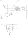
図1(a)は、本実施形態の電流制限装置の構成を示すブロック図である。 FIG. 1A is a block diagram showing the configuration of the current limiting device of this embodiment.
図1(a)に示すように、本実施形態の電流制限装置3は、電源1と外部負荷2の間の電流経路に設けられるP−MOSFETによるスイッチ31と、上記電流経路に挿入される電流検出用の抵抗32と、電流制限装置3の動作を制御する制御部33と、制御部33の指令に応じてP−MOSFETによるスイッチ34を介してスイッチ31をオン、オフさせるスイッチ制御回路35と、抵抗32に発生する電圧に基づいて電流を監視する電流監視回路36と、を備える。なお、電流制限装置の極性を反転させ、N−MOSFETを使用した回路とすることもできる。
As shown in FIG. 1A, the current
また、図1(a)に示すように、電流制限装置3には、基準電圧源41およびオペアンプ42からなる電流制限手段としての定電流回路が設けられる。オペアンプ42は、抵抗32に発生する電圧が基準電圧源41の基準電圧に等しくなるようにスイッチ31のゲートにフィードバックをかけることで、定電流特性を得ている。
As shown in FIG. 1A, the current
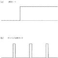
図2は、電流制限装置3の動作モードを示す図であり、図2(a)は外部負荷2を動作させる通常モードを、図2(b)は外部負荷2を動作させないときのオンパルス診断モードを、それぞれ示している。
2A and 2B are diagrams showing an operation mode of the current
図2(a)は、通常モードにおける電源の立ち上がり時を示しており、非動作状態にあった外部負荷2の動作を開始させる場合に相当する。 FIG. 2A shows the power-on time in the normal mode, and corresponds to the case where the operation of the external load 2 in a non-operating state is started.
図3は、電流制限が働く閾値を示す図である。 FIG. 3 is a diagram illustrating threshold values at which current limiting works.
電流監視回路36は、抵抗32に流れる電流を監視しており、定電流回路は、抵抗32に一定電流値(閾値B)以上の電流が流れてから所定時間(t0)経過後に定電流動作を開始し、電流が閾値Bで制限される。経過時間t0は、オペアンプ42の位相補償回路の定数や、反転入力端子への遅延回路の追加により調整できる。図1(b)は遅延回路の例を示しており、この例では、抵抗およびコンデンサからなる遅延回路43を追加している。
The
制御部33は、抵抗32に一定電流値(閾値C)以上の電流が流れてから所定時間(t1)継続して電流が閾値C1を越えている場合に過電流と判断し、スイッチ制御回路35によりスイッチ34をオンし、スイッチ31をオフして回路を遮断する。
The
一方、図2(b)に示すオンパルス診断モードでは、動作していない外部負荷2に短時間のオンパルスを与えることで、外部負荷2を動作させない範囲での導通状態を診断している。これにより、待機中の外部負荷2および回路について診断を行うことができる。 On the other hand, in the on-pulse diagnosis mode shown in FIG. 2B, a short-time on-pulse is given to the external load 2 that is not operating, thereby diagnosing a conduction state in a range where the external load 2 is not operated. Thereby, it is possible to diagnose the standby external load 2 and the circuit.
制御部33は、閾値C2を超えると過電流と判定してもよい。このように、動作モードに応じて、過電流の検出値を閾値C1および閾値C2の間で区別してもよい。
The
本実施形態の電流検出装置3において、通常モード時に過電流が検出された場合に、出力を一度オフして外部負荷2の動作を停止させ、オンパルス診断モードに移行することで、復帰可能か否かの診断を行うことができる。なお、電流制限装置3では、外部負荷2の動作時にもオフパルス診断を実行可能だが、その説明は省略する。
In the
外部負荷2の側で短絡が発生するなど過電流となる事象が発生した場合、以下に示すような動作となる。
(1)抵抗32にスイッチ31をカットオフさせるレベルの電圧が発生する電流が流れると、その値で電流が制限される(閾値A)。
(2)上記の定電流回路が機能すると電流を一定値に制限する(閾値B)。
(3)電流監視回路36により過電流が検出されると、制御部33はスイッチ制御回路35を介してスイッチ31をオフし、電流を遮断する(閾値C1または閾値C2)。
When an overcurrent event such as a short circuit occurs on the external load 2 side, the following operation is performed.
(1) When a current that generates a voltage that cuts off the
(2) When the above constant current circuit functions, the current is limited to a constant value (threshold value B).
(3) When an overcurrent is detected by the
図3の太線に示すように、以上の3段階での電流制限により、スイッチ31の素子限界曲線を超える電流を流さないように電流制限領域を設定することができる。なお、図3では、過電流検出の検出値が閾値C1の場合の電流制限領域を示している。
As shown by the thick line in FIG. 3, the current limiting region can be set so as not to flow a current exceeding the element limit curve of the
上記のように、本実施形態の電流制限装置3では、定電流回路が機能するまでの間、閾値Bでの電流制限を行わない。このため、図3に示すように、突入電流のピークを抑制することなく突入電流が許容され、早期に電流値が定常状態に移行し電流値が迅速に正常値に向かって収束する。これにより、外部負荷2を速やかに動作状態に移行させることができる。また、これまで扱えなかった突入電流を許容することで、従来接続できなかったランプや容量性負荷なども接続可能となる。また、電流値が早期に正常範囲に収束するため、過電流の誤検出を防ぎつつ、短時間での診断を実行できる。
As described above, the current
従来、オンパルス診断では、1つのパルスについて特定の1回のタイミングでの電流値を取得し、その電流値に基づいて過電流を検出している。これに対し、オンパルス診断における1回のパルス中で複数回、電流値を獲得し、電流波形を認識するようにしてもよい。 Conventionally, in the on-pulse diagnosis, a current value at a specific timing is acquired for one pulse, and an overcurrent is detected based on the current value. On the other hand, the current value may be acquired and the current waveform may be recognized a plurality of times in one pulse in the on-pulse diagnosis.
図4(a)は、種々の電流波形について電流値を高速サンプリングする例を示している。この例では、電流制限手段および制御手段としての制御部33は、スイッチ31がオンした直後の過渡期間内(1パルスの期間内)に電流監視回路36を介して電流値を複数回にわたり取得する。また、制御部33は、取得した電流値に基づいて、突入電流を識別する。そして、突入電流と認識した場合には、過電流の異常と判定しない。
FIG. 4A shows an example in which current values are sampled at high speed for various current waveforms. In this example, the
このように、高速サンプリングの結果を制御部33において処理することにより電流波形が認識できるため、過電流と突入電流とを区別することが可能となる。図4(a)の例では、突入許容領域を設けることで、過電流検出の閾値を下げることなく、突入電流を正常と認識することが可能となる。
Thus, since the current waveform can be recognized by processing the result of the high-speed sampling in the
図4(b)は、パルスの立ち下がり直前に1回だけ電流値を検出する従来の診断結果と、図4(a)の高速サンプリングの診断結果を比較した例を示している。この例では、従来の診断において突入電流を正常と判定する条件では、図4(a)に示す過電流Pを検出できないのに対し、高速サンプリングによれば、突入電流と過電流Pとを的確に区別できることを示している。 FIG. 4B shows an example in which a conventional diagnosis result in which the current value is detected once just before the fall of the pulse is compared with the high-speed sampling diagnosis result in FIG. In this example, it is not possible to detect the overcurrent P shown in FIG. 4A under the condition that the inrush current is determined to be normal in the conventional diagnosis. On the other hand, according to the high speed sampling, the inrush current and the overcurrent P are accurately determined. Can be distinguished.
以上説明したように、本発明の電流制限装置によれば、電流制限手段はスイッチが閉じられてから所定時間経過後に動作を開始するため、スイッチを閉じた直後の突入電流を許容できる。また、本発明の電流制限装置によれば、スイッチが閉じられてからの過渡期間に複数回にわたり取得された電流値に基づいて電流制限の可否を決定するので、上記過渡期間における突入電流を許容することができる。 As described above, according to the current limiting device of the present invention, the current limiting means starts operation after a predetermined time has elapsed since the switch was closed, and therefore can accept an inrush current immediately after the switch is closed. In addition, according to the current limiting device of the present invention, whether to limit the current is determined based on the current value acquired a plurality of times during the transition period after the switch is closed. can do.
本発明の適用範囲は上記実施形態に限定されることはない。本発明は、回路の電流値を制限して過電流を防止する電流制限装置に対し、広く適用することができる。 The scope of application of the present invention is not limited to the above embodiment. The present invention can be widely applied to a current limiting device that limits the current value of a circuit to prevent an overcurrent.
3 電流制限装置
31 スイッチ
42 オペアンプ(電流制限手段、定電流回路)
41 基準電圧源(電流制限手段、定電流回路)
33 制御部(電流制限手段、制御手段)
3 Current Limiting
41 Reference voltage source (current limiting means, constant current circuit)
33 Control section (current limiting means, control means)
Claims (3)
回路の電流を一定の電流値以下に制限する電流制限手段と、
前記回路を開閉するスイッチと、
を備え、
前記電流制限手段は、一定電流値以上の電流が流れてから所定時間経過後に動作を開始することを特徴とする電流制限装置。 In the current limiting device that limits the current value of the circuit to prevent overcurrent,
Current limiting means for limiting the circuit current to a certain current value or less;
A switch for opening and closing the circuit;
With
The current limiting device is characterized in that the current limiting device starts an operation after a predetermined time has elapsed since a current of a predetermined current value or more flows.
回路の電流を一定の電流値以下に制限する電流制限手段と、
前記回路を開閉するスイッチと、
前記スイッチが閉じられてからの過渡期間に複数回にわたり取得された電流値に基づいて前記電流制限手段による電流制限の可否を決定する制御手段と、
を備えることを特徴とする電流制限装置。 In the current limiting device that limits the current value of the circuit to prevent overcurrent,
Current limiting means for limiting the circuit current to a certain current value or less;
A switch for opening and closing the circuit;
Control means for determining whether or not the current limiting means can limit current based on a current value acquired a plurality of times during a transition period after the switch is closed;
A current limiting device comprising:
Priority Applications (1)
| Application Number | Priority Date | Filing Date | Title |
|---|---|---|---|
| JP2007270803A JP5429439B2 (en) | 2007-10-18 | 2007-10-18 | Current limiting device |
Applications Claiming Priority (1)
| Application Number | Priority Date | Filing Date | Title |
|---|---|---|---|
| JP2007270803A JP5429439B2 (en) | 2007-10-18 | 2007-10-18 | Current limiting device |
Publications (2)
| Publication Number | Publication Date |
|---|---|
| JP2009100582A true JP2009100582A (en) | 2009-05-07 |
| JP5429439B2 JP5429439B2 (en) | 2014-02-26 |
Family
ID=40703079
Family Applications (1)
| Application Number | Title | Priority Date | Filing Date |
|---|---|---|---|
| JP2007270803A Expired - Fee Related JP5429439B2 (en) | 2007-10-18 | 2007-10-18 | Current limiting device |
Country Status (1)
| Country | Link |
|---|---|
| JP (1) | JP5429439B2 (en) |
Cited By (4)
| Publication number | Priority date | Publication date | Assignee | Title |
|---|---|---|---|---|
| JP2017135848A (en) * | 2016-01-27 | 2017-08-03 | 京セラ株式会社 | Power conditioner and distributed power source system |
| WO2017163903A1 (en) * | 2016-03-24 | 2017-09-28 | 株式会社オートネットワーク技術研究所 | Power feed control device |
| JP2018074746A (en) * | 2016-10-28 | 2018-05-10 | 京セラドキュメントソリューションズ株式会社 | Motor control device and image formation apparatus |
| JP2019205332A (en) * | 2018-05-23 | 2019-11-28 | 廣達電腦股▲ふん▼有限公司Quanta Computer Inc. | Battery unit and operation method thereof |
Citations (6)
| Publication number | Priority date | Publication date | Assignee | Title |
|---|---|---|---|---|
| JPH0525945U (en) * | 1991-09-13 | 1993-04-02 | 日本無線株式会社 | Current limit circuit |
| JP2001095139A (en) * | 1999-09-22 | 2001-04-06 | Yazaki Corp | Method and apparatus for circuit cut-off on overcurrent |
| JP2001238350A (en) * | 2000-02-28 | 2001-08-31 | Nec Corp | Method and circuit for overcurrent protection |
| JP2004236405A (en) * | 2003-01-29 | 2004-08-19 | Auto Network Gijutsu Kenkyusho:Kk | Overcurrent protective circuit |
| JP2005206204A (en) * | 2004-01-23 | 2005-08-04 | Takazono Sangyo Co Ltd | Controlling apparatus for sealing apparatus and dividedly packaging machine |
| JP2007020390A (en) * | 2005-07-06 | 2007-01-25 | Phoenix Contact Gmbh & Co Kg | Method for supplying power to load of low voltage, which is protected by protection device, and electronic power supply device |
-
2007
- 2007-10-18 JP JP2007270803A patent/JP5429439B2/en not_active Expired - Fee Related
Patent Citations (6)
| Publication number | Priority date | Publication date | Assignee | Title |
|---|---|---|---|---|
| JPH0525945U (en) * | 1991-09-13 | 1993-04-02 | 日本無線株式会社 | Current limit circuit |
| JP2001095139A (en) * | 1999-09-22 | 2001-04-06 | Yazaki Corp | Method and apparatus for circuit cut-off on overcurrent |
| JP2001238350A (en) * | 2000-02-28 | 2001-08-31 | Nec Corp | Method and circuit for overcurrent protection |
| JP2004236405A (en) * | 2003-01-29 | 2004-08-19 | Auto Network Gijutsu Kenkyusho:Kk | Overcurrent protective circuit |
| JP2005206204A (en) * | 2004-01-23 | 2005-08-04 | Takazono Sangyo Co Ltd | Controlling apparatus for sealing apparatus and dividedly packaging machine |
| JP2007020390A (en) * | 2005-07-06 | 2007-01-25 | Phoenix Contact Gmbh & Co Kg | Method for supplying power to load of low voltage, which is protected by protection device, and electronic power supply device |
Cited By (9)
| Publication number | Priority date | Publication date | Assignee | Title |
|---|---|---|---|---|
| JP2017135848A (en) * | 2016-01-27 | 2017-08-03 | 京セラ株式会社 | Power conditioner and distributed power source system |
| JP2020048412A (en) * | 2016-01-27 | 2020-03-26 | 京セラ株式会社 | Power conditioner and distributed power source system |
| WO2017163903A1 (en) * | 2016-03-24 | 2017-09-28 | 株式会社オートネットワーク技術研究所 | Power feed control device |
| JP2017175809A (en) * | 2016-03-24 | 2017-09-28 | 株式会社オートネットワーク技術研究所 | Power supply control device |
| CN108701990A (en) * | 2016-03-24 | 2018-10-23 | 株式会社自动网络技术研究所 | Power supply control apparatus |
| US10770884B2 (en) | 2016-03-24 | 2020-09-08 | Autonetworks Technologies, Ltd. | Power supply control apparatus |
| CN108701990B (en) * | 2016-03-24 | 2021-04-13 | 株式会社自动网络技术研究所 | Power supply control device |
| JP2018074746A (en) * | 2016-10-28 | 2018-05-10 | 京セラドキュメントソリューションズ株式会社 | Motor control device and image formation apparatus |
| JP2019205332A (en) * | 2018-05-23 | 2019-11-28 | 廣達電腦股▲ふん▼有限公司Quanta Computer Inc. | Battery unit and operation method thereof |
Also Published As
| Publication number | Publication date |
|---|---|
| JP5429439B2 (en) | 2014-02-26 |
Similar Documents
| Publication | Publication Date | Title |
|---|---|---|
| US10038436B2 (en) | Masking vd to vref after miller plateau and gate charge | |
| JP6632794B2 (en) | System for powering a load coupled from an input node to an output node | |
| TWI448029B (en) | A system and method for protecting a power conversion system under open circuit and / or short circuit conditions | |
| US8045310B2 (en) | Semiconductor device with overcurrent protection | |
| JP2020182258A (en) | Driving device, power supply system, and test method of driving device | |
| TW201508296A (en) | Detecting faults in hot-swap applications | |
| JP2006296119A (en) | Drive circuit of semiconductor switching element | |
| WO2017215335A1 (en) | Igbt short-circuit protection circuit and method, igbt driver and igbt circuit | |
| JP2008202997A (en) | Temperature detection circuit | |
| JP2008109776A (en) | Dc/dc converter | |
| JP5429439B2 (en) | Current limiting device | |
| JP4882710B2 (en) | Load drive device failure detection device and load drive IC | |
| JP2005328589A (en) | Switching regulator control circuit and switching regulator | |
| JP2000308253A (en) | Controller and method for power supply | |
| JP5258810B2 (en) | Semiconductor device testing equipment | |
| JP6811163B2 (en) | Load drive | |
| JP5144292B2 (en) | Switching power supply circuit and vehicle equipped with the same | |
| JP4148243B2 (en) | Abnormality detection circuit | |
| JP6753348B2 (en) | Switching element drive circuit | |
| JP2020129867A (en) | Overcurrent detection circuit and current output circuit | |
| JP4415384B2 (en) | DIGITAL OUTPUT DEVICE AND DIAGNOSIS METHOD USING DIGITAL OUTPUT DEVICE | |
| US11777438B2 (en) | Motor drive device | |
| JP5370915B2 (en) | Voltage limiting circuit | |
| JP2004086257A (en) | Abnormality detection device | |
| JP2004327783A (en) | Device for detecting abnormality, and method therefor |
Legal Events
| Date | Code | Title | Description |
|---|---|---|---|
| A621 | Written request for application examination |
Free format text: JAPANESE INTERMEDIATE CODE: A621 Effective date: 20100922 |
|
| A977 | Report on retrieval |
Free format text: JAPANESE INTERMEDIATE CODE: A971007 Effective date: 20120611 |
|
| A131 | Notification of reasons for refusal |
Free format text: JAPANESE INTERMEDIATE CODE: A131 Effective date: 20120619 |
|
| A521 | Written amendment |
Free format text: JAPANESE INTERMEDIATE CODE: A523 Effective date: 20120724 |
|
| A131 | Notification of reasons for refusal |
Free format text: JAPANESE INTERMEDIATE CODE: A131 Effective date: 20130327 |
|
| A521 | Written amendment |
Free format text: JAPANESE INTERMEDIATE CODE: A523 Effective date: 20130515 |
|
| TRDD | Decision of grant or rejection written | ||
| A01 | Written decision to grant a patent or to grant a registration (utility model) |
Free format text: JAPANESE INTERMEDIATE CODE: A01 Effective date: 20131106 |
|
| A61 | First payment of annual fees (during grant procedure) |
Free format text: JAPANESE INTERMEDIATE CODE: A61 Effective date: 20131119 |
|
| R150 | Certificate of patent or registration of utility model |
Free format text: JAPANESE INTERMEDIATE CODE: R150 |
|
| LAPS | Cancellation because of no payment of annual fees |