JP2009094326A - Method of grinding wafer - Google Patents
Method of grinding wafer Download PDFInfo
- Publication number
- JP2009094326A JP2009094326A JP2007264172A JP2007264172A JP2009094326A JP 2009094326 A JP2009094326 A JP 2009094326A JP 2007264172 A JP2007264172 A JP 2007264172A JP 2007264172 A JP2007264172 A JP 2007264172A JP 2009094326 A JP2009094326 A JP 2009094326A
- Authority
- JP
- Japan
- Prior art keywords
- grinding
- wafer
- back surface
- chuck table
- grinding wheel
- Prior art date
- Legal status (The legal status is an assumption and is not a legal conclusion. Google has not performed a legal analysis and makes no representation as to the accuracy of the status listed.)
- Pending
Links
- 238000000034 method Methods 0.000 title claims abstract description 9
- 238000005452 bending Methods 0.000 claims abstract description 17
- 230000000694 effects Effects 0.000 claims abstract description 10
- 238000005247 gettering Methods 0.000 claims abstract description 10
- 239000006061 abrasive grain Substances 0.000 claims abstract description 8
- 229910003460 diamond Inorganic materials 0.000 claims abstract description 7
- 239000010432 diamond Substances 0.000 claims abstract description 7
- 230000003746 surface roughness Effects 0.000 claims abstract description 7
- 229910001385 heavy metal Inorganic materials 0.000 claims abstract description 6
- 230000001681 protective effect Effects 0.000 claims description 6
- XLYOFNOQVPJJNP-UHFFFAOYSA-N water Substances O XLYOFNOQVPJJNP-UHFFFAOYSA-N 0.000 claims description 6
- 239000002245 particle Substances 0.000 claims description 2
- 239000004575 stone Substances 0.000 abstract description 4
- 235000012431 wafers Nutrition 0.000 description 43
- XUIMIQQOPSSXEZ-UHFFFAOYSA-N Silicon Chemical compound [Si] XUIMIQQOPSSXEZ-UHFFFAOYSA-N 0.000 description 2
- 230000003028 elevating effect Effects 0.000 description 2
- 229910052710 silicon Inorganic materials 0.000 description 2
- 239000010703 silicon Substances 0.000 description 2
- RYGMFSIKBFXOCR-UHFFFAOYSA-N Copper Chemical compound [Cu] RYGMFSIKBFXOCR-UHFFFAOYSA-N 0.000 description 1
- 229910052802 copper Inorganic materials 0.000 description 1
- 239000010949 copper Substances 0.000 description 1
- 230000000593 degrading effect Effects 0.000 description 1
- 239000013585 weight reducing agent Substances 0.000 description 1
Images


Classifications
-
- H—ELECTRICITY
- H01—ELECTRIC ELEMENTS
- H01L—SEMICONDUCTOR DEVICES NOT COVERED BY CLASS H10
- H01L21/00—Processes or apparatus adapted for the manufacture or treatment of semiconductor or solid state devices or of parts thereof
- H01L21/02—Manufacture or treatment of semiconductor devices or of parts thereof
- H01L21/04—Manufacture or treatment of semiconductor devices or of parts thereof the devices having potential barriers, e.g. a PN junction, depletion layer or carrier concentration layer
- H01L21/18—Manufacture or treatment of semiconductor devices or of parts thereof the devices having potential barriers, e.g. a PN junction, depletion layer or carrier concentration layer the devices having semiconductor bodies comprising elements of Group IV of the Periodic Table or AIIIBV compounds with or without impurities, e.g. doping materials
- H01L21/30—Treatment of semiconductor bodies using processes or apparatus not provided for in groups H01L21/20 - H01L21/26
- H01L21/302—Treatment of semiconductor bodies using processes or apparatus not provided for in groups H01L21/20 - H01L21/26 to change their surface-physical characteristics or shape, e.g. etching, polishing, cutting
-
- B—PERFORMING OPERATIONS; TRANSPORTING
- B24—GRINDING; POLISHING
- B24D—TOOLS FOR GRINDING, BUFFING OR SHARPENING
- B24D7/00—Bonded abrasive wheels, or wheels with inserted abrasive blocks, designed for acting otherwise than only by their periphery, e.g. by the front face; Bushings or mountings therefor
- B24D7/18—Wheels of special form
-
- B—PERFORMING OPERATIONS; TRANSPORTING
- B24—GRINDING; POLISHING
- B24B—MACHINES, DEVICES, OR PROCESSES FOR GRINDING OR POLISHING; DRESSING OR CONDITIONING OF ABRADING SURFACES; FEEDING OF GRINDING, POLISHING, OR LAPPING AGENTS
- B24B1/00—Processes of grinding or polishing; Use of auxiliary equipment in connection with such processes
-
- B—PERFORMING OPERATIONS; TRANSPORTING
- B24—GRINDING; POLISHING
- B24B—MACHINES, DEVICES, OR PROCESSES FOR GRINDING OR POLISHING; DRESSING OR CONDITIONING OF ABRADING SURFACES; FEEDING OF GRINDING, POLISHING, OR LAPPING AGENTS
- B24B7/00—Machines or devices designed for grinding plane surfaces on work, including polishing plane glass surfaces; Accessories therefor
- B24B7/20—Machines or devices designed for grinding plane surfaces on work, including polishing plane glass surfaces; Accessories therefor characterised by a special design with respect to properties of the material of non-metallic articles to be ground
- B24B7/22—Machines or devices designed for grinding plane surfaces on work, including polishing plane glass surfaces; Accessories therefor characterised by a special design with respect to properties of the material of non-metallic articles to be ground for grinding inorganic material, e.g. stone, ceramics, porcelain
- B24B7/228—Machines or devices designed for grinding plane surfaces on work, including polishing plane glass surfaces; Accessories therefor characterised by a special design with respect to properties of the material of non-metallic articles to be ground for grinding inorganic material, e.g. stone, ceramics, porcelain for grinding thin, brittle parts, e.g. semiconductors, wafers
Landscapes
- Engineering & Computer Science (AREA)
- Mechanical Engineering (AREA)
- Chemical & Material Sciences (AREA)
- Ceramic Engineering (AREA)
- Inorganic Chemistry (AREA)
- Physics & Mathematics (AREA)
- Condensed Matter Physics & Semiconductors (AREA)
- General Physics & Mathematics (AREA)
- Manufacturing & Machinery (AREA)
- Computer Hardware Design (AREA)
- Microelectronics & Electronic Packaging (AREA)
- Power Engineering (AREA)
- Mechanical Treatment Of Semiconductor (AREA)
- Grinding Of Cylindrical And Plane Surfaces (AREA)
Abstract
Description
本発明は、ウェーハの裏面を研削して抗折強度を向上させる方法に関するものである。 The present invention relates to a method for improving the bending strength by grinding the back surface of a wafer.
IC、LSI等のデバイスが複数形成されたウェーハは、裏面が研削されて所定の厚さに形成された後に、個々のデバイスに分割されて各種電子機器に利用されている。近年は、電子機器の小型化、軽量化等の要望に応えるために、デバイスに分割される前のウェーハについてもより薄型化を図ることが求められている。 A wafer on which a plurality of devices such as IC and LSI are formed is ground into a predetermined thickness by grinding the back surface, and then divided into individual devices and used for various electronic devices. In recent years, in order to meet demands for downsizing, weight reduction, and the like of electronic devices, it is required to make the wafer before being divided into devices thinner.
ところが、ウェーハの裏面が研磨され、例えばウェーハの厚さが100μm以下というように薄く形成されると、ウェーハに含有された銅等の重金属の動きを抑制するゲッタリング効果が低下し、ウェーハから切り出されるデバイスの品質を低下させるという問題がある。 However, when the back surface of the wafer is polished, for example, when the thickness of the wafer is thin such as 100 μm or less, the gettering effect that suppresses the movement of heavy metals such as copper contained in the wafer is reduced, and the wafer is cut out from the wafer. There is a problem of degrading the quality of the device.
そこで、ウェーハの裏面を研削して歪み層を形成することによりゲッタリング効果を生じさせ、かかるゲッタリング効果により重金属の動きを抑制する技術が提案されている(例えば特許文献1参照)。 Therefore, a technique has been proposed in which a gettering effect is generated by grinding the back surface of a wafer to form a strained layer, and the movement of heavy metals is suppressed by the gettering effect (see, for example, Patent Document 1).
しかし、ウェーハの裏面に歪み層を形成すると、ウェーハから切り出されるデバイスの抗折強度が低下して品質及び寿命が低下するという問題がある。 However, when a strained layer is formed on the back surface of the wafer, there is a problem that the bending strength of the device cut out from the wafer is lowered and the quality and life are lowered.
そこで、本発明が解決しようとする課題は、ウェーハの裏面を研削した場合において、ウェーハ及びデバイスの抗折強度を低下させることなく、ゲッタリング効果を生じさせることである。 Therefore, the problem to be solved by the present invention is to produce a gettering effect without reducing the bending strength of the wafer and the device when the back surface of the wafer is ground.
本発明は、ウェーハを保持するチャックテーブルと、チャックテーブルに保持されたウェーハを研削する回転可能な研削ホイールを有する研削手段とを備えた研削装置を用い、表面に複数のデバイスが形成されたウェーハの裏面を研削してゲッタリング効果により重金属の遊動を抑制すると共に抗折強度を略1000MPa以上に維持するウェーハの研削方法に関するもので、研削ホイールは、基台の自由端部に粒径1μm以下のダイヤモンド砥粒がビトリファイドボンドで固定された研削砥石が固着されて構成され、ウェーハの表面に保護部材を貼着し保護部材を該チャックテーブルに対面させて保持し、チャックテーブルを回転させながら研削ホイールを回転させ、研削砥石によってウェーハの裏面を研削して裏面の面粗さの平均値を0.003μm以下とし、ウェーハの裏面に残存する歪み層の厚さを0.05μmとする。 The present invention uses a grinding apparatus having a chuck table for holding a wafer and a grinding means having a rotatable grinding wheel for grinding the wafer held on the chuck table, and a wafer having a plurality of devices formed on the surface thereof This invention relates to a method for grinding a wafer that grinds the back surface of the wafer and suppresses the movement of heavy metals by the gettering effect and maintains the bending strength at about 1000 MPa or more. The grinding wheel has a particle size of 1 μm or less at the free end of the base. Grinding wheel with diamond abrasive grains fixed by vitrified bond is fixed, and a protective member is attached to the wafer surface, the protective member is held facing the chuck table, and grinding is performed while rotating the chuck table. Rotate the wheel and grind the back surface of the wafer with a grinding wheel to reduce the average surface roughness of the back surface to 0 And 003μm or less, the thickness of the strained layer remaining on the back surface of the wafer and 0.05 .mu.m.
チャックテーブルの回転速度は100〜400rpmであり、研削ホイールの回転速度は1000〜6000rpmであり、研削手段の研削送り速度は0.05〜0.5μm/秒であり、研削水の使用量は2〜10リットル/分であることが望ましい。 The rotation speed of the chuck table is 100 to 400 rpm, the rotation speed of the grinding wheel is 1000 to 6000 rpm, the grinding feed speed of the grinding means is 0.05 to 0.5 μm / second, and the amount of grinding water used is 2 Desirably, it is 10 liters / minute.
本発明では、粒径が1μm以下のダイヤモンド砥粒がビトリファイドボンドで固定された研削砥石を用い、ウェーハの裏面の面粗さの平均値が0.003μm、裏面に残存する歪み層の厚さが0.05μmとなるようにウェーハの裏面を研削することにより、デバイスの抗折強度が1000MPa以上となると共にゲッタリング効果を生じさせることができる。 In the present invention, a grinding wheel in which diamond abrasive grains having a grain size of 1 μm or less are fixed by vitrified bonds, the average value of the surface roughness of the back surface of the wafer is 0.003 μm, and the thickness of the strained layer remaining on the back surface is By grinding the back surface of the wafer so as to be 0.05 μm, the bending strength of the device becomes 1000 MPa or more and a gettering effect can be produced.
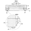
図1に示す研削装置1は、ウェーハを研削して所望の厚さに仕上げることができる装置であり、ウェーハを保持するチャックテーブル2と、チャックテーブル2に保持されたウェーハを研削する研削手段3とを備えている。 A grinding apparatus 1 shown in FIG. 1 is an apparatus that can grind a wafer and finish it to a desired thickness. A grinding table 3 that holds a wafer and a grinding means 3 that grinds the wafer held on the chuck table 2. And.
チャックテーブル2は、水平方向に移動可能であると共に回転可能であり、図示しないモータによって駆動されて所定の回転速度で回転することができる。 The chuck table 2 can move in the horizontal direction and can rotate, and can be driven by a motor (not shown) to rotate at a predetermined rotation speed.
研削手段3は、垂直方向の軸心を有するスピンドル30と、スピンドル30を回転可能に支持するハウジング31と、スピンドル30に連結されスピンドル30を回転駆動するモータ32と、スピンドル30の下端に形成されたホイールマウント33と、ホイールマウント33に固定される研削ホイール34と、研削水が流入する流入口35とから構成され、研削ホイール34は、モータ32によって駆動されて所定の回転速度で回転することができる。
The grinding means 3 is formed at a lower end of the
研削手段3は、研削送り手段4によって垂直方向に研削送りされる。研削送り手段4は、垂直方向に配設されたボールネジ40と、ボールネジ40と平行に配設された一対のガイドレール41と、ボールネジ40を回動させるパルスモータ42と、図示しないナットがボールネジ40に螺合すると共に側部がガイドレール41に摺接し切削手段3を保持する昇降部43とから構成され、パルスモータ42に駆動されてボールネジ40が回動し昇降部43がガイドレール41にガイドされて昇降するのに伴い研削手段3も所定の送り速度で昇降する構成となっている。
The grinding means 3 is ground and fed in the vertical direction by the grinding feed means 4. The grinding feed means 4 includes a
図2に示すように、研削ホイール34はリング状の基台340と、基台340の自由端部に円弧状に固着された複数の研削砥石341とから構成される。研削砥石341は、例えばダイヤモンド砥粒をビトリファイドボンドで固定して構成される。
As shown in FIG. 2, the
図3に示すように、基台340にはスピンドル30の内部に形成された流路300に連通して垂直方向に水を流す流路342が形成されており、ウェーハの研削時には、図1に示した流入口35から流入した研削水が流路300及び流路342を通じてウェーハと研削砥石341との接触部位に対して供給される。研削時における各種条件は、図1に示す操作部5から入力することができる。
As shown in FIG. 3, the
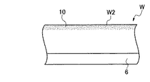
図4に示すように、ウェーハWの表面W1には分割予定ラインSに区画されて複数のデバイスDが形成されている。裏面W2の研削にあたり、表面W1にはデバイスDを保護するための保護部材6が貼着され、図5に示すように、表裏を反転して裏面W2が上を向いた状態とする。
As shown in FIG. 4, a plurality of devices D are formed on the front surface W <b> 1 of the wafer W so as to be partitioned into division planned lines S. In grinding the back surface W2, a
そして、図6に示すように、チャックテーブル2において保護部材6側を保持して裏面W2を露出させた状態で研削手段3の下方に移動させ、研削ホイール34を回転させると共に研削送り手段4によって研削手段3を下降させていき、回転する研削砥石341を裏面W2に接触させ、ウェーハWが所定の厚さになるまで裏面W2を研削する。そうすると、図7に示すように、裏面W2には歪み層10が形成される。
Then, as shown in FIG. 6, the chuck table 2 is moved below the grinding means 3 while holding the
図2、3、6に示した研削砥石341として、粒径が1μm以下のダイヤモンド砥粒をビトリファイドボンドで固めた砥石(以下「砥石A」という。)と、平均粒径が2μmのダイヤモンド砥粒をビトリファイドボンドで固めた砥石(以下「砥石B」という。)とを用意した。そして、砥石Aを用いて複数のシリコンウェーハの裏面を研削すると共に、砥石Bを用いて複数のシリコンウェーハの裏面を研削した。
The
砥石Aによる研削時の条件と砥石Bによる研削時の条件とは、砥粒の粒径以外については同様とし、各条件は、下記に示す範囲で変化させた。
チャックテーブル2の回転速度:100〜400[rpm]
研削ホイール34の回転速度:1000〜6000[rpm]
研削手段3の研削送り速度:0.05〜0.5[μm/秒]
研削手段3における研削水使用量:2〜10[リットル/分]
The conditions at the time of grinding with the grindstone A and the conditions at the time of grinding with the grindstone B were the same except for the grain size of the abrasive grains, and each condition was changed within the following range.
Rotation speed of chuck table 2: 100 to 400 [rpm]
Rotational speed of grinding wheel 34: 1000 to 6000 [rpm]
Grinding feed rate of the grinding means 3: 0.05 to 0.5 [μm / sec]
Amount of grinding water used in the grinding means 3: 2 to 10 [liter / minute]
研削後は、すべてのウェーハについて、裏面(研削面)の面粗さを測定した。面粗さとしては、JISB0601(ISO4287)で規定される算術平均粗さ(Ra)及び最大高さ(Ry)を用いた。 After grinding, the surface roughness of the back surface (grind surface) was measured for all wafers. As the surface roughness, arithmetic average roughness (Ra) and maximum height (Ry) defined by JISB0601 (ISO4287) were used.
砥石Aによる研削では、研削後のウェーハの裏面の算術平均粗さ(Ra)の最大値が0.003[μm]であり、最大高さ(Ry)の最大値が0.012[μm]であった。また、裏面に残存する歪み層の厚さの平均値は0.05[μm]であった。 In grinding with the grinding wheel A, the maximum value of the arithmetic average roughness (Ra) of the back surface of the wafer after grinding is 0.003 [μm], and the maximum value of the maximum height (Ry) is 0.012 [μm]. there were. The average value of the thickness of the strained layer remaining on the back surface was 0.05 [μm].
一方、砥石Bによる研削では、研削後のウェーハの裏面の算術平均粗さ(Ra)の最大値が0.006μmであり、最大高さ(Ry)の最大値が0.044μmであった。また、裏面に残存する歪み層の厚さの平均値は0.08[μm]であった。 On the other hand, in grinding with the grindstone B, the maximum value of the arithmetic mean roughness (Ra) of the back surface of the wafer after grinding was 0.006 μm, and the maximum value of the maximum height (Ry) was 0.044 μm. The average thickness of the strained layer remaining on the back surface was 0.08 [μm].
次に、砥石A及び砥石Bによって裏面が研削されたすべてのウェーハを同一のダイシング装置によって個々のデバイスに分割し、その中からデバイスをランダムに取り出して抗折強度を求めた。抗折強度としては、球抗折試験による抗折強度を用いた。 Next, all the wafers whose back surfaces were ground by the grindstone A and the grindstone B were divided into individual devices by the same dicing apparatus, and the devices were randomly taken out of them to obtain the bending strength. As the bending strength, the bending strength by the ball bending test was used.
砥石Aによって研削されたウェーハから切り出されたデバイスの抗折強度の最大値は2364[MPa]、最小値は998[MPa]であり、平均値は1638[MPa]であった。一方、砥石Bによって研削されたウェーハから切り出されたデバイスの抗折強度の最大値は953[MPa]、最小値は476[MPa]であり、平均値は650[MPa]であった。 The maximum value of the bending strength of the device cut out from the wafer ground by the grindstone A was 2364 [MPa], the minimum value was 998 [MPa], and the average value was 1638 [MPa]. On the other hand, the maximum value of the bending strength of the device cut out from the wafer ground by the grindstone B was 953 [MPa], the minimum value was 476 [MPa], and the average value was 650 [MPa].
上記結果が示すように、砥石Aを用いた場合は、砥石Bを用いた場合と比較して、面粗さ及び抗折強度が改善されることが確認された。また、歪み層の厚さの平均値が0.05[μm]であることで、ゲッタリング効果によりウェーハ内部の重金属の動きを抑制することができる。更に、厚さの平均値が0.05[μm]である歪み層を形成しつつ、デバイスの抗折強度も略1000[MPa]以上に維持することができた。デバイスの抗折強度を略1000[MPa]以上とすることにより、そのデバイスが利用される電子機器の品質の安定性を保つことができる。 As shown by the above results, it was confirmed that when the grindstone A was used, the surface roughness and the bending strength were improved as compared with the case where the grindstone B was used. In addition, since the average value of the thickness of the strained layer is 0.05 [μm], the movement of heavy metal inside the wafer can be suppressed by the gettering effect. Furthermore, the bending strength of the device could be maintained at about 1000 [MPa] or more while forming a strained layer having an average thickness of 0.05 [μm]. By setting the bending strength of the device to approximately 1000 [MPa] or more, it is possible to maintain the stability of the quality of the electronic device in which the device is used.
1:研削装置
2:チャックテーブル
3:研削手段
30:スピンドル 31:ハウジング 32:モータ 33:ホイールマウント
34:研削ホイール 340:基台 341:研削砥石 342:流路
35:流入口
4:研削送り手段
40:ボールネジ 41:ガイドレール 42:パルスモータ 43:昇降部
5:操作部
W:ウェーハ
W1:表面 S:分割予定ライン D:デバイス
W2:裏面
10:歪み層
1: Grinding device 2: Chuck table 3: Grinding means 30: Spindle 31: Housing 32: Motor 33: Wheel mount 34: Grinding wheel 340: Base 341: Grinding wheel 342: Channel 35: Inlet port 4: Grinding feed means 40: Ball screw 41: Guide rail 42: Pulse motor 43: Lifting unit 5: Operation unit W: Wafer W1: Front surface S: Divided line D: Device W2: Back surface 10: Strain layer
Claims (2)
該研削ホイールは、基台の自由端部に粒径1μm以下のダイヤモンド砥粒がビトリファイドボンドで固定された研削砥石が固着されて構成され、
ウェーハの表面に保護部材を貼着し該保護部材を該チャックテーブルに対面させて保持し、
該チャックテーブルを回転させながら該研削ホイールを回転させ、該研削砥石によって該ウェーハの裏面を研削して該裏面の面粗さの平均値を0.003μm以下とし、
該ウェーハの裏面に残存する歪み層の厚さを0.05μmとする
ウェーハの研削方法。 Using a grinding apparatus comprising a chuck table for holding a wafer and a grinding means having a rotatable grinding wheel for grinding the wafer held on the chuck table, the back surface of the wafer having a plurality of devices formed on the surface A method for grinding a wafer, which suppresses the heavy metal movement by the gettering effect by grinding and maintains the bending strength at about 1000 MPa or more,
The grinding wheel is composed of a grinding wheel in which diamond abrasive grains having a particle diameter of 1 μm or less are fixed to a free end of a base with vitrified bonds,
A protective member is attached to the surface of the wafer and the protective member is held facing the chuck table,
Rotating the grinding wheel while rotating the chuck table, grinding the back surface of the wafer with the grinding wheel to an average value of the surface roughness of the back surface of 0.003 μm or less,
A wafer grinding method in which the thickness of the strained layer remaining on the back surface of the wafer is 0.05 μm.
Priority Applications (5)
| Application Number | Priority Date | Filing Date | Title |
|---|---|---|---|
| JP2007264172A JP2009094326A (en) | 2007-10-10 | 2007-10-10 | Method of grinding wafer |
| TW097131913A TW200917372A (en) | 2007-10-10 | 2008-08-21 | Grinding method for wafer |
| KR1020080092271A KR20090037302A (en) | 2007-10-10 | 2008-09-19 | Method for grinding wafer |
| US12/243,483 US7677955B2 (en) | 2007-10-10 | 2008-10-01 | Grinding method for wafer |
| CNA2008101685918A CN101407035A (en) | 2007-10-10 | 2008-10-10 | Grinding method for wafer |
Applications Claiming Priority (1)
| Application Number | Priority Date | Filing Date | Title |
|---|---|---|---|
| JP2007264172A JP2009094326A (en) | 2007-10-10 | 2007-10-10 | Method of grinding wafer |
Publications (1)
| Publication Number | Publication Date |
|---|---|
| JP2009094326A true JP2009094326A (en) | 2009-04-30 |
Family
ID=40534711
Family Applications (1)
| Application Number | Title | Priority Date | Filing Date |
|---|---|---|---|
| JP2007264172A Pending JP2009094326A (en) | 2007-10-10 | 2007-10-10 | Method of grinding wafer |
Country Status (5)
| Country | Link |
|---|---|
| US (1) | US7677955B2 (en) |
| JP (1) | JP2009094326A (en) |
| KR (1) | KR20090037302A (en) |
| CN (1) | CN101407035A (en) |
| TW (1) | TW200917372A (en) |
Cited By (11)
| Publication number | Priority date | Publication date | Assignee | Title |
|---|---|---|---|---|
| CN103056737A (en) * | 2011-10-21 | 2013-04-24 | 株式会社迪思科 | Grinding method for sapphire substrate |
| DE102015211806A1 (en) | 2014-06-27 | 2015-12-31 | Disco Corporation | processing device |
| DE102015211805A1 (en) | 2014-06-27 | 2015-12-31 | Disco Corporation | Evaluation procedure for device wafers |
| KR20160033041A (en) * | 2014-09-17 | 2016-03-25 | 가부시기가이샤 디스코 | Method for grinding workpiece |
| CN105437053A (en) * | 2014-06-18 | 2016-03-30 | 上海和辉光电有限公司 | Panel grinder |
| DE102017205104A1 (en) | 2016-03-28 | 2017-09-28 | Disco Corporation | WORK EVALUATION PROCESS |
| CN107403738A (en) * | 2016-05-19 | 2017-11-28 | 株式会社迪思科 | Go the evaluation method of defect |
| JP2018056384A (en) * | 2016-09-29 | 2018-04-05 | 株式会社ディスコ | Processing method for device wafer |
| JP2018531503A (en) * | 2015-08-14 | 2018-10-25 | エム キューブド テクノロジーズ, インコーポレイテッド | Machine with highly controllable processing tools for finishing workpieces |
| JP2019013989A (en) * | 2017-07-04 | 2019-01-31 | 株式会社ディスコ | Grinder |
| KR20210033897A (en) | 2019-09-19 | 2021-03-29 | 가부시기가이샤 디스코 | Treatment method of wafer and chip measurement apparatus |
Families Citing this family (20)
| Publication number | Priority date | Publication date | Assignee | Title |
|---|---|---|---|---|
| JP5568837B2 (en) * | 2008-02-29 | 2014-08-13 | 株式会社Sumco | Silicon substrate manufacturing method |
| JP2011029331A (en) * | 2009-07-23 | 2011-02-10 | Disco Abrasive Syst Ltd | Method for grinding wafer and protective tape |
| JP2011151070A (en) * | 2010-01-19 | 2011-08-04 | Disco Abrasive Syst Ltd | Processing method for wafer |
| JP5550940B2 (en) * | 2010-02-23 | 2014-07-16 | 株式会社ディスコ | Transport mechanism |
| WO2012119616A1 (en) | 2011-03-10 | 2012-09-13 | Peter Wolters Gmbh | Method and device for the single-sided processing of flat workpieces |
| CN102198616B (en) * | 2011-04-18 | 2013-07-17 | 武汉飞米思科技有限公司 | Plane grinding method for engineering ceramic workpiece |
| US9266220B2 (en) | 2011-12-30 | 2016-02-23 | Saint-Gobain Abrasives, Inc. | Abrasive articles and method of forming same |
| JP2014172146A (en) * | 2013-03-12 | 2014-09-22 | Disco Abrasive Syst Ltd | Grinding wheel |
| JP6040947B2 (en) * | 2014-02-20 | 2016-12-07 | 信越半導体株式会社 | Double-head grinding method for workpieces |
| JP6353684B2 (en) * | 2014-04-04 | 2018-07-04 | 株式会社ディスコ | Grinding wheel and grinding chamber cleaning method |
| SE540285C2 (en) * | 2015-01-20 | 2018-05-22 | Htc Sweden Ab | System comprising a carrier disk and a floor grinding machine |
| JP2016168660A (en) * | 2015-03-13 | 2016-09-23 | 株式会社ディスコ | Grinding wheel |
| JP6489973B2 (en) * | 2015-07-30 | 2019-03-27 | 株式会社ディスコ | Grinding equipment |
| JP6523872B2 (en) * | 2015-08-27 | 2019-06-05 | 株式会社ディスコ | Grinding device |
| JP6908464B2 (en) * | 2016-09-15 | 2021-07-28 | 株式会社荏原製作所 | Substrate processing method and substrate processing equipment |
| JP6719825B2 (en) * | 2016-10-12 | 2020-07-08 | 株式会社ディスコ | Grinding apparatus and wafer processing method |
| JP7012454B2 (en) * | 2017-04-27 | 2022-01-28 | 株式会社岡本工作機械製作所 | Manufacturing method of electrostatic suction chuck and manufacturing method of semiconductor device |
| JP6951152B2 (en) * | 2017-08-22 | 2021-10-20 | 株式会社ディスコ | Grinding device |
| JP7204318B2 (en) * | 2017-11-06 | 2023-01-16 | 株式会社ディスコ | grinding wheel |
| JP7049848B2 (en) * | 2018-02-08 | 2022-04-07 | 株式会社ディスコ | How to grind the holding surface |
Citations (4)
| Publication number | Priority date | Publication date | Assignee | Title |
|---|---|---|---|---|
| JP2003332276A (en) * | 2002-05-13 | 2003-11-21 | Hitachi Chem Co Ltd | Method of manufacturing semiconductor device |
| JP2006012902A (en) * | 2004-06-22 | 2006-01-12 | Disco Abrasive Syst Ltd | Wafer processing method |
| JP2006203132A (en) * | 2005-01-24 | 2006-08-03 | Disco Abrasive Syst Ltd | Method of grinding wafer |
| JP2007012810A (en) * | 2005-06-29 | 2007-01-18 | Renesas Technology Corp | Method of manufacturing semiconductor integrated circuit device |
Family Cites Families (10)
| Publication number | Priority date | Publication date | Assignee | Title |
|---|---|---|---|---|
| US7255637B2 (en) * | 2000-09-08 | 2007-08-14 | Applied Materials, Inc. | Carrier head vibration damping |
| SG119140A1 (en) * | 2001-07-04 | 2006-02-28 | Disco Corp | Grinding wheel |
| JP4759948B2 (en) | 2004-07-28 | 2011-08-31 | ルネサスエレクトロニクス株式会社 | Manufacturing method of semiconductor device |
| JP2006108532A (en) * | 2004-10-08 | 2006-04-20 | Disco Abrasive Syst Ltd | Method of grinding wafer |
| CA2588332A1 (en) * | 2004-12-01 | 2006-06-08 | Rhodius Schleifwerkzeuge Gmbh & Co. Kg | Device for cutting and grinding, chucking device and rotating tool with vibration damping |
| DE102006030559A1 (en) * | 2006-07-03 | 2008-01-10 | Robert Bosch Gmbh | Electric hand tool |
| JP4961183B2 (en) * | 2006-09-26 | 2012-06-27 | 株式会社ディスコ | Semiconductor wafer processing method |
| JP4913517B2 (en) * | 2006-09-26 | 2012-04-11 | 株式会社ディスコ | Wafer grinding method |
| JP4986568B2 (en) * | 2006-10-11 | 2012-07-25 | 株式会社ディスコ | Wafer grinding method |
| JP2009004406A (en) * | 2007-06-19 | 2009-01-08 | Disco Abrasive Syst Ltd | Working method for substrate |
-
2007
- 2007-10-10 JP JP2007264172A patent/JP2009094326A/en active Pending
-
2008
- 2008-08-21 TW TW097131913A patent/TW200917372A/en unknown
- 2008-09-19 KR KR1020080092271A patent/KR20090037302A/en not_active Application Discontinuation
- 2008-10-01 US US12/243,483 patent/US7677955B2/en active Active
- 2008-10-10 CN CNA2008101685918A patent/CN101407035A/en active Pending
Patent Citations (4)
| Publication number | Priority date | Publication date | Assignee | Title |
|---|---|---|---|---|
| JP2003332276A (en) * | 2002-05-13 | 2003-11-21 | Hitachi Chem Co Ltd | Method of manufacturing semiconductor device |
| JP2006012902A (en) * | 2004-06-22 | 2006-01-12 | Disco Abrasive Syst Ltd | Wafer processing method |
| JP2006203132A (en) * | 2005-01-24 | 2006-08-03 | Disco Abrasive Syst Ltd | Method of grinding wafer |
| JP2007012810A (en) * | 2005-06-29 | 2007-01-18 | Renesas Technology Corp | Method of manufacturing semiconductor integrated circuit device |
Cited By (26)
| Publication number | Priority date | Publication date | Assignee | Title |
|---|---|---|---|---|
| CN103056737A (en) * | 2011-10-21 | 2013-04-24 | 株式会社迪思科 | Grinding method for sapphire substrate |
| CN105437053A (en) * | 2014-06-18 | 2016-03-30 | 上海和辉光电有限公司 | Panel grinder |
| CN105215839B (en) * | 2014-06-27 | 2019-02-15 | 株式会社迪思科 | Processing unit (plant) |
| DE102015211806A1 (en) | 2014-06-27 | 2015-12-31 | Disco Corporation | processing device |
| DE102015211805A1 (en) | 2014-06-27 | 2015-12-31 | Disco Corporation | Evaluation procedure for device wafers |
| KR20160001637A (en) | 2014-06-27 | 2016-01-06 | 가부시기가이샤 디스코 | Method for evaluating device wafer |
| KR20160001627A (en) | 2014-06-27 | 2016-01-06 | 가부시기가이샤 디스코 | Processing apparatus |
| CN105215839A (en) * | 2014-06-27 | 2016-01-06 | 株式会社迪思科 | Processing unit (plant) |
| US9679820B2 (en) | 2014-06-27 | 2017-06-13 | Disco Corporation | Evaluation method of device wafer |
| KR20160033041A (en) * | 2014-09-17 | 2016-03-25 | 가부시기가이샤 디스코 | Method for grinding workpiece |
| KR102197502B1 (en) | 2014-09-17 | 2020-12-31 | 가부시기가이샤 디스코 | Method for grinding workpiece |
| JP2018531503A (en) * | 2015-08-14 | 2018-10-25 | エム キューブド テクノロジーズ, インコーポレイテッド | Machine with highly controllable processing tools for finishing workpieces |
| US10157802B2 (en) | 2016-03-28 | 2018-12-18 | Disco Corporation | Workpiece evaluating method |
| DE102017205104B4 (en) | 2016-03-28 | 2019-08-01 | Disco Corporation | WORK EVALUATION PROCESS |
| DE102017205104A1 (en) | 2016-03-28 | 2017-09-28 | Disco Corporation | WORK EVALUATION PROCESS |
| KR20170113216A (en) | 2016-03-28 | 2017-10-12 | 가부시기가이샤 디스코 | Method of evaluating workpiece |
| US10068811B2 (en) | 2016-05-19 | 2018-09-04 | Disco Corporation | Method of evaluating gettering property |
| KR20170131244A (en) | 2016-05-19 | 2017-11-29 | 가부시기가이샤 디스코 | Evaluation method of gettering property |
| CN107403738A (en) * | 2016-05-19 | 2017-11-28 | 株式会社迪思科 | Go the evaluation method of defect |
| CN107403738B (en) * | 2016-05-19 | 2022-10-11 | 株式会社迪思科 | Method for evaluating defect removal performance |
| JP2018056384A (en) * | 2016-09-29 | 2018-04-05 | 株式会社ディスコ | Processing method for device wafer |
| JP2019013989A (en) * | 2017-07-04 | 2019-01-31 | 株式会社ディスコ | Grinder |
| JP7067878B2 (en) | 2017-07-04 | 2022-05-16 | 株式会社ディスコ | Grinding device |
| KR20210033897A (en) | 2019-09-19 | 2021-03-29 | 가부시기가이샤 디스코 | Treatment method of wafer and chip measurement apparatus |
| US11637039B2 (en) | 2019-09-19 | 2023-04-25 | Disco Corporation | Method of processing wafer, and chip measuring apparatus |
| US11901234B2 (en) | 2019-09-19 | 2024-02-13 | Disco Corporation | Method of processing wafer, and chip measuring apparatus |
Also Published As
| Publication number | Publication date |
|---|---|
| CN101407035A (en) | 2009-04-15 |
| KR20090037302A (en) | 2009-04-15 |
| US20090098808A1 (en) | 2009-04-16 |
| US7677955B2 (en) | 2010-03-16 |
| TW200917372A (en) | 2009-04-16 |
Similar Documents
| Publication | Publication Date | Title |
|---|---|---|
| JP2009094326A (en) | Method of grinding wafer | |
| JP5226287B2 (en) | Wafer grinding method | |
| JP2010225987A (en) | Polishing method of wafer and polishing pad | |
| JP2008114336A (en) | Self-grinding method for chuck table | |
| JP6192778B2 (en) | Silicon wafer processing equipment | |
| CN105609414B (en) | Method for grinding workpiece | |
| JP2007335521A (en) | Method for grinding outer periphery of wafer | |
| JP6631829B2 (en) | Flatness / flatness correction method for lapping machines and grinding wheels | |
| JP2008207302A (en) | Grinding wheel dressing method and dressing tool | |
| JP2009269128A (en) | Grinding device and grinding method | |
| JP5127270B2 (en) | Dressing method and dresser board | |
| JP2010219461A (en) | Wafer polishing method | |
| CN111438580B (en) | Method for processing object to be processed | |
| JP2010194672A (en) | Method of grinding workpiece | |
| JP5389433B2 (en) | Grinding wheel | |
| JP6812068B2 (en) | Processing method | |
| JP2012222123A (en) | Method for grinding semiconductor wafer | |
| JP2009095947A (en) | Grinder and grinding method of wafer | |
| JP2021098238A (en) | Workpiece grinding method | |
| JP2019062147A (en) | Protective member processing method | |
| JP2023049160A (en) | Workpiece grinding method | |
| JP2022133007A (en) | Grinding method for work-piece | |
| JP2023180612A (en) | Work-piece grinding method | |
| JP2023077743A (en) | Grinding wheel and grinding method of workpiece | |
| JP2023109277A (en) | Grinding method |
Legal Events
| Date | Code | Title | Description |
|---|---|---|---|
| A621 | Written request for application examination |
Free format text: JAPANESE INTERMEDIATE CODE: A621 Effective date: 20100924 |
|
| A977 | Report on retrieval |
Free format text: JAPANESE INTERMEDIATE CODE: A971007 Effective date: 20120928 |
|
| A131 | Notification of reasons for refusal |
Free format text: JAPANESE INTERMEDIATE CODE: A131 Effective date: 20121002 |
|
| A521 | Request for written amendment filed |
Free format text: JAPANESE INTERMEDIATE CODE: A523 Effective date: 20121130 |
|
| A02 | Decision of refusal |
Free format text: JAPANESE INTERMEDIATE CODE: A02 Effective date: 20130108 |