JP2009074855A - Photodetection device - Google Patents
Photodetection device Download PDFInfo
- Publication number
- JP2009074855A JP2009074855A JP2007242470A JP2007242470A JP2009074855A JP 2009074855 A JP2009074855 A JP 2009074855A JP 2007242470 A JP2007242470 A JP 2007242470A JP 2007242470 A JP2007242470 A JP 2007242470A JP 2009074855 A JP2009074855 A JP 2009074855A
- Authority
- JP
- Japan
- Prior art keywords
- light receiving
- light
- receiving element
- receiving elements
- voltage
- Prior art date
- Legal status (The legal status is an assumption and is not a legal conclusion. Google has not performed a legal analysis and makes no representation as to the accuracy of the status listed.)
- Pending
Links
- 238000001514 detection method Methods 0.000 claims abstract description 28
- 230000003287 optical effect Effects 0.000 claims description 14
- 230000007274 generation of a signal involved in cell-cell signaling Effects 0.000 claims description 2
- 238000006243 chemical reaction Methods 0.000 description 12
- 230000035945 sensitivity Effects 0.000 description 10
- 238000010586 diagram Methods 0.000 description 4
- 230000000903 blocking effect Effects 0.000 description 3
- 230000000694 effects Effects 0.000 description 2
- 238000000034 method Methods 0.000 description 2
- 230000006750 UV protection Effects 0.000 description 1
- 230000001413 cellular effect Effects 0.000 description 1
- 239000004973 liquid crystal related substance Substances 0.000 description 1
- 230000007257 malfunction Effects 0.000 description 1
- 230000037072 sun protection Effects 0.000 description 1
Images


Classifications
-
- G—PHYSICS
- G01—MEASURING; TESTING
- G01J—MEASUREMENT OF INTENSITY, VELOCITY, SPECTRAL CONTENT, POLARISATION, PHASE OR PULSE CHARACTERISTICS OF INFRARED, VISIBLE OR ULTRAVIOLET LIGHT; COLORIMETRY; RADIATION PYROMETRY
- G01J1/00—Photometry, e.g. photographic exposure meter
- G01J1/10—Photometry, e.g. photographic exposure meter by comparison with reference light or electric value provisionally void
- G01J1/16—Photometry, e.g. photographic exposure meter by comparison with reference light or electric value provisionally void using electric radiation detectors
- G01J1/1626—Arrangements with two photodetectors, the signals of which are compared
-
- G—PHYSICS
- G01—MEASURING; TESTING
- G01J—MEASUREMENT OF INTENSITY, VELOCITY, SPECTRAL CONTENT, POLARISATION, PHASE OR PULSE CHARACTERISTICS OF INFRARED, VISIBLE OR ULTRAVIOLET LIGHT; COLORIMETRY; RADIATION PYROMETRY
- G01J1/00—Photometry, e.g. photographic exposure meter
- G01J1/42—Photometry, e.g. photographic exposure meter using electric radiation detectors
- G01J1/44—Electric circuits
-
- G—PHYSICS
- G01—MEASURING; TESTING
- G01J—MEASUREMENT OF INTENSITY, VELOCITY, SPECTRAL CONTENT, POLARISATION, PHASE OR PULSE CHARACTERISTICS OF INFRARED, VISIBLE OR ULTRAVIOLET LIGHT; COLORIMETRY; RADIATION PYROMETRY
- G01J1/00—Photometry, e.g. photographic exposure meter
- G01J1/02—Details
-
- G—PHYSICS
- G01—MEASURING; TESTING
- G01J—MEASUREMENT OF INTENSITY, VELOCITY, SPECTRAL CONTENT, POLARISATION, PHASE OR PULSE CHARACTERISTICS OF INFRARED, VISIBLE OR ULTRAVIOLET LIGHT; COLORIMETRY; RADIATION PYROMETRY
- G01J1/00—Photometry, e.g. photographic exposure meter
- G01J1/10—Photometry, e.g. photographic exposure meter by comparison with reference light or electric value provisionally void
- G01J1/20—Photometry, e.g. photographic exposure meter by comparison with reference light or electric value provisionally void intensity of the measured or reference value being varied to equalise their effects at the detectors, e.g. by varying incidence angle
- G01J1/28—Photometry, e.g. photographic exposure meter by comparison with reference light or electric value provisionally void intensity of the measured or reference value being varied to equalise their effects at the detectors, e.g. by varying incidence angle using variation of intensity or distance of source
- G01J1/30—Photometry, e.g. photographic exposure meter by comparison with reference light or electric value provisionally void intensity of the measured or reference value being varied to equalise their effects at the detectors, e.g. by varying incidence angle using variation of intensity or distance of source using electric radiation detectors
- G01J1/32—Photometry, e.g. photographic exposure meter by comparison with reference light or electric value provisionally void intensity of the measured or reference value being varied to equalise their effects at the detectors, e.g. by varying incidence angle using variation of intensity or distance of source using electric radiation detectors adapted for automatic variation of the measured or reference value
-
- H—ELECTRICITY
- H01—ELECTRIC ELEMENTS
- H01L—SEMICONDUCTOR DEVICES NOT COVERED BY CLASS H10
- H01L31/00—Semiconductor devices sensitive to infrared radiation, light, electromagnetic radiation of shorter wavelength or corpuscular radiation and specially adapted either for the conversion of the energy of such radiation into electrical energy or for the control of electrical energy by such radiation; Processes or apparatus specially adapted for the manufacture or treatment thereof or of parts thereof; Details thereof
- H01L31/02—Details
- H01L31/02016—Circuit arrangements of general character for the devices
- H01L31/02019—Circuit arrangements of general character for the devices for devices characterised by at least one potential jump barrier or surface barrier
-
- H—ELECTRICITY
- H01—ELECTRIC ELEMENTS
- H01L—SEMICONDUCTOR DEVICES NOT COVERED BY CLASS H10
- H01L31/00—Semiconductor devices sensitive to infrared radiation, light, electromagnetic radiation of shorter wavelength or corpuscular radiation and specially adapted either for the conversion of the energy of such radiation into electrical energy or for the control of electrical energy by such radiation; Processes or apparatus specially adapted for the manufacture or treatment thereof or of parts thereof; Details thereof
- H01L31/08—Semiconductor devices sensitive to infrared radiation, light, electromagnetic radiation of shorter wavelength or corpuscular radiation and specially adapted either for the conversion of the energy of such radiation into electrical energy or for the control of electrical energy by such radiation; Processes or apparatus specially adapted for the manufacture or treatment thereof or of parts thereof; Details thereof in which radiation controls flow of current through the device, e.g. photoresistors
- H01L31/09—Devices sensitive to infrared, visible or ultraviolet radiation
Abstract
Description
本発明は、電子機器の筐体に照射される照射光の強さを検出する光検出装置に関する。 The present invention relates to a light detection device that detects the intensity of irradiation light applied to a casing of an electronic device.
従来から、携帯電話等の電子機器が用いられる環境の明るさを検知するために、その筐体(ケース)に照射される照射光の強さを検出する光検出装置が知られている。かかる光検出装置においては、筐体に設けられた開口を経た入射光に感応する受光素子によって得られる光信号によって照射光の強さを検出している。 Conventionally, in order to detect the brightness of an environment in which an electronic device such as a mobile phone is used, a light detection device that detects the intensity of irradiation light applied to the casing (case) is known. In such a light detection device, the intensity of irradiation light is detected by an optical signal obtained by a light receiving element that is sensitive to incident light that has passed through an opening provided in a housing.
ところで、当該受光素子は、電子機器の筐体の内壁等からの反射・散乱若しくは電子機器の筐体表面からの反射・散乱によって生じた迷光によって発生する暗電流も同時に検出している。 By the way, the light receiving element simultaneously detects dark current generated by stray light caused by reflection / scattering from the inner wall of the casing of the electronic device or reflection / scattering from the surface of the casing of the electronic device.
また、上述した迷光による暗電流以外にも受光素子の熱や逆バイアス変動によって暗電流が発生する。更に、受光素子の1例としてのフォトダイオードにおいては、フォトダイオードの周囲温度変化によって暗電流が変化する。 In addition to the dark current due to the stray light described above, dark current is generated by heat of the light receiving element and reverse bias fluctuation. Furthermore, in a photodiode as an example of a light receiving element, the dark current changes due to a change in ambient temperature of the photodiode.
かかる暗電流の発生やその変動によって、電子機器への照射光の強さを正確に検出することが出来ないという問題点があり、また、これによって、光検出装置からの光検出信号出力によって駆動する駆動装置における誤作動の原因ともなっていた。 Due to the occurrence of such dark current and its fluctuations, there is a problem that the intensity of light applied to the electronic device cannot be detected accurately, and in this way, it is driven by the light detection signal output from the light detection device. It was also a cause of malfunction in the driving device.
上述した問題点を解決する方法として、暗電流をキャンセルしつつ、照射光の強さを検出する方法が、特許文献1乃至3に開示されている。 As a method for solving the above-described problems, Patent Documents 1 to 3 disclose a method of detecting the intensity of irradiation light while canceling a dark current.
特許文献1は、光軸上に配置されていないキャンセル用受光素子による迷光の受光により発生した電流を任意の電圧に変換し、当該変換した任意の電圧を基準電圧として光軸上に配置された受光素子からの信号光及び迷光によって生じた電流を電圧に変換することが開示されている。 Patent Document 1 converts a current generated by receiving stray light by a canceling light receiving element not arranged on the optical axis into an arbitrary voltage, and arranges the converted arbitrary voltage on the optical axis as a reference voltage. It is disclosed to convert a current generated by signal light and stray light from a light receiving element into a voltage.
特許文献2は、光軸上に配置されていないキャンセル用受光素子から発生した熱や逆バイアスの変動による暗電流を任意の電圧に変換し、当該変換した任意の電圧を基準電圧として光軸上に配置された受光素子からの信号光によって生じた電流を電圧に変換することが開示されている。 Patent Document 2 converts dark current due to fluctuations in heat and reverse bias generated from a canceling light receiving element not arranged on the optical axis into an arbitrary voltage, and uses the converted arbitrary voltage as a reference voltage on the optical axis. Converting the current generated by the signal light from the light receiving element arranged in the voltage into a voltage.
特許文献3には、光源からの信号光の光軸上に設けられた受光素子と、光軸上以外に設けられて信号光を受光しないキャンセル用受光素子とを接続点を介して直列接続されて、当該接続点と接地電位との間に設けられた抵抗に流れる電流を測定することが開示されている。
特許文献1乃至3に記載されている光検出装置は、キャンセル用の受光素子を光軸上とは異なる位置に配置し又は遮光のための構造によって信号光を遮光することによって暗電流のみを測定し、光軸上にある受光素子から発生する光電流をかかる暗電流を基準に電圧への変換又は光電流からかかる暗電流を差し引いた電流を電圧へ変換することにより、暗電流の影響を抑制可能としている。 The photodetectors described in Patent Documents 1 to 3 measure only dark current by disposing a light receiving element for cancellation at a position different from the optical axis, or by shielding signal light by a structure for shielding light. The effect of the dark current is suppressed by converting the photocurrent generated from the light-receiving element on the optical axis into a voltage based on the dark current or converting the current obtained by subtracting the dark current from the photocurrent into a voltage. It is possible.
しかしながら、キャンセル用の受光素子を光軸上とは異なる位置に設けることによって、受光素子と変換器や基準電位との配線又は受光素子同士の配線が複雑且つ長くなることによって、光検出装置の消費電力が大きくなるという問題点があった。 However, by providing a canceling light receiving element at a position different from the optical axis, the wiring between the light receiving element and the converter, the reference potential, or the wiring between the light receiving elements becomes complicated and long. There was a problem that electric power became large.
また、遮光のための構造によって低コスト化が困難となることや、受光素子の配置上の制約によって光検出装置の小型化が困難になる問題点もあった。 In addition, there is a problem that it is difficult to reduce the cost due to the structure for shielding light, and it is difficult to reduce the size of the light detection device due to restrictions on the arrangement of the light receiving elements.
本発明は、以上の如き事情に鑑みてなされたものであり、外部光を遮光することなく、暗電流の影響を抑制して小型で消費電力が少ない光検出装置を提供することを目的としている。 The present invention has been made in view of the circumstances as described above, and an object of the present invention is to provide a photodetection device that is small and consumes less power by suppressing the influence of dark current without shielding external light. .
上述した課題を解決するために、本発明は、電子機器の筐体に照射される照射光の強さを検出する光検出装置であって、互いに異なる受光波長特性を有して中間点を介して互いに直列接続され且つ前記筐体の開口に臨んで配置された2つの受光素子と、前記受光素子の直列接続回路の両端を基準電位に維持する基準電位回路と、前記中間点から抽出される電流の大きさに応じた光検出信号を生成する信号生成回路と、を含む光検出装置を提供する。 In order to solve the above-described problems, the present invention is a photodetection device that detects the intensity of irradiation light applied to a casing of an electronic device, and has different light-receiving wavelength characteristics via an intermediate point. Two light receiving elements connected in series with each other and facing the opening of the housing, a reference potential circuit for maintaining both ends of the series connection circuit of the light receiving elements at a reference potential, and extracted from the intermediate point Provided is a light detection device including a signal generation circuit that generates a light detection signal in accordance with the magnitude of a current.
更に、前記筐体の開口を経た入射光を前記2つの受光素子に中継する光学系を含んでいても良い。 Furthermore, an optical system that relays incident light that has passed through the opening of the housing to the two light receiving elements may be included.
また、前記受光素子のうち一方の高感度受光波長領域が他方のそれよりも広くても良い。 Also, one of the light receiving elements may have a higher sensitivity light receiving wavelength region than that of the other.
また、前記基準電位回路の基準電位は接地電位若しくは定電圧電位であっても良い。 The reference potential of the reference potential circuit may be a ground potential or a constant voltage potential.
本発明の光検出装置においては、互いに異なる受光波長特性を有して、中間点を介して接続され且つ電子機器の筐体の開口に臨んで配置された2つの受光素子を含み、当該受光素子の直列回路の両端を基準電位に維持しつつ当該中間点から抽出される電流の大きさを検出する構成としたので、消費電力の低減及び光検出装置自体の小型化を実現することが出来る。 The light detection device of the present invention includes two light receiving elements that have different light receiving wavelength characteristics, are connected via an intermediate point, and are disposed facing the opening of the casing of the electronic device. Since the configuration is such that the magnitude of the current extracted from the intermediate point is detected while maintaining both ends of the series circuit at the reference potential, it is possible to reduce power consumption and downsize the photodetector itself.
以下、本発明の実施例について添付図面を参照しつつ詳細に説明する。 Hereinafter, embodiments of the present invention will be described in detail with reference to the accompanying drawings.
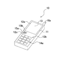
図1は、本発明の実施例としての光検出装置を備える携帯電話を示す斜視図である。 FIG. 1 is a perspective view showing a mobile phone provided with a photodetecting device as an embodiment of the present invention.
図1に示されているように、携帯電話10の筐体11には複数の開口12a、12b、12cが設けられている。開口12aは、筐体10の主面上方に設けられており、開口12aには、表示部13が収められている。筐体10の主面下方に設けられた複数の開口12bには、ボタン操作部の各ボタン14aが収められている。表示部13とボタン14aとの間に位置するように設けられた開口12cは、受光用であり、これを介して入射する外部光に応答する2つの受光波長特性の互いに異なる受光素子15a、15bが収められている。受光素子15a、15bはいずれも遮光されずに開口12cに臨んで設けられている。受光素子15a、15bは例えば、フォトダイオードである。筐体11の上方の側面部分にはアンテナ16aが設けられている。なお、筐体11の少なくとも開口12cの周縁近傍は不透明である方が望ましい。
As shown in FIG. 1, the
なお、光検出装置を備える装置として本実施例では携帯電話としているが、携帯電話に限られることなく、PDA、ノート型パソコン、腕時計若しくはデジタルカメラ等の移動若しくは携帯自在な電子機器であっても良い。また、外部光は太陽光に限らずレーザ光等の光であっても良い。 In the present embodiment, a mobile phone is provided as a device including a photodetection device. However, the mobile phone is not limited to a mobile phone, and may be a mobile or portable electronic device such as a PDA, a notebook computer, a wristwatch, or a digital camera. good. The external light is not limited to sunlight, and may be light such as laser light.
図2は、受光素子15a、15bの波長λ[nm]に対する受光感度[A/W]の関係すなわち受光波長特性を示したグラフである。グラフの横軸が波長であり、グラフの縦軸が受光感度を示している。受光素子15aの受光波長特性を破線21によって示し、受光素子15bの受光波長特性を実線22によって示している
図2に示されたグラフから判るように、受光素子15aは、約320nmから約400nmまでの波長範囲において高い受光感度を有している(例えば、かかる高受光感度を有する領域を紫外線領域Aとする)。これに対して、受光素子15bは、約280nmから約400nmまでの波長範囲において高い受光感度を有している(例えば、かかる高受光感度を有する領域を紫外線領域Bとする)。従って、受光素子15a、15bは、異なる受光波長特性を有する。受光素子15aが紫外線領域Aに高受光感度を有する狭域受光素子であり、受光素子15bが紫外線領域Aよりも広い紫外線領域Bに高受光感度を有する広域受光素子である。
FIG. 2 is a graph showing the relationship of the light receiving sensitivity [A / W] with respect to the wavelength λ [nm] of the
なお、受光素子15a、15bの受光波長特性は、図2で示されているような紫外線領域において高い受光感度を有する特性に限定されることなく、例えば、可視光領域や赤外線領域において高い受光感度を有していても良い。
The light receiving wavelength characteristics of the
図3は、本発明の実施例としての光検出装置を備える携帯電話10の回路構成を示している。
FIG. 3 shows a circuit configuration of a
図3に示されているように、制御部31は、表示部13を構成する液晶パネル等の表示パネル13aが接続されている。制御部31は、アンテナ16aを備える通信部16をボタン操作部14からの制御入力に応じて制御する。制御部31には、光検出装置32が更に接続されている。光検出装置32は、筐体11の受光用の開口12cに臨み互いに直列接続された受光素子15a、15b及び受光素子15a、15bの接続点に接続された電流−電圧変換増幅器33を含んでいる。
As shown in FIG. 3, the
制御部31は、アンテナ16aからの受信する電波信号に応じた受信番号を表示パネル13aに表示し、ボタン操作部14からの制御入力に応じた操作画面を表示パネル13aに表示する。また、制御部31は、電流−電圧変換増幅器33にて受光素子15a、15bの受光によって発生した光電流の差に応じた電圧に変換された光検出信号を受信し、かかる光検出信号を演算して照射光の紫外線の強さを示す紫外線指数を表示部13に表示する。紫外線指数は、例えば、紫外線の防止効果を示す数値のSPF(Sun Protection Factor:紫外線防止指数)であっても良い。
The
図4は、本発明の第1の実施例としての光検出装置を示している。図4に示されているように、光検出装置32は、互いに異なる受光波長特性を有する受光素子15a、15bを含む。例えば、受光素子15a、15bは、図2に示した受光波長特性を有する。受光素子15a、15bは、中間点T1を介して互いに直列に接続され、中間点T1は、電流−電圧変換増幅器33の入力端に接続されている。電流−電圧変換増幅器33は、オペアンプ41、フィードバック抵抗42から構成されている。
FIG. 4 shows a photodetecting device as a first embodiment of the present invention. As shown in FIG. 4, the
受光素子15aのアノードと受光素子15bのカソードとが接続され、受光素子15aのカソードと受光素子15bのアノードとが接地電位に接続されている。すなわち、受光素子15a、15bの直列回路の両端が接地電位の基準電位に維持されている。また、受光素子15aのアノードと受光素子15bのカソードとの接続の中間点T1は、オペアンプ41の負入力端子に接続されている。
The anode of the
オペアンプ41の正入力端子及び負電源端子は、接地電位に接続されている。また、オペアンプ41の正電源端子は、電源Vddに接続されている。更に、オペアンプ41の負入力端子とオペアンプ41の出力とがフィードバック抵抗42を介して接続されている。
The positive input terminal and the negative power supply terminal of the
次に、本実施例の光検出装置の動作について説明する。紫外線が破線矢印にて示すように照射された場合に、受光素子15aには紫外線領域Aの波長の紫外線を受光すると、矢印IAの方向に向かって受光量に応じた光電流Iaが流れる。また、受光素子15bが紫外線領域Bの波長の紫外線を受光すると、矢印IBの方向に向かって受光量に応じた光電流Ibが流れる。中間点T1には、光電流Ibから光電流Iaを差し引いた差分電流Icが矢印ICの方向に向かって電流−電圧変換増幅器33から抽出されることになる。差分電流Icは、出力点T2に出力電圧Vとして出力される。更に、出力電圧Vは、出力Voutから光検出装置32の外部に出力される。
Next, the operation of the photodetecting device of this embodiment will be described. When the ultraviolet ray is irradiated as indicated by the broken arrow, when the ultraviolet ray having the wavelength in the ultraviolet region A is received by the
上述したように、光電流Iaは紫外線領域Aの紫外線光に対応した光電流であり、光電流Ibは紫外線領域Bの紫外線光に対応した光電流である故、中間点T1に流れる差分電流Icは、紫外線の波長が約280nmから320nm(例えば、紫外線領域Cとする)の紫外線光に対応する光電流の電流量となり、紫外線領域Cのみの紫外光量を測定したこととなる。 As described above, the light current Ia is a light current corresponding to the ultraviolet light in the ultraviolet region A, because the light current Ib is an optical current corresponding to the ultraviolet light in the ultraviolet region B, the differential current flowing to the midpoint T 1 Ic is the amount of photocurrent corresponding to ultraviolet light having an ultraviolet wavelength of about 280 nm to 320 nm (for example, the ultraviolet region C), and the ultraviolet light amount only in the ultraviolet region C is measured.
また、受光素子15a、15bからそれぞれ受光素子の熱による暗電流が発生していても、光電流Ibから光電流Iaを差し引く差分電流Icにおいては、かかる暗電流も相殺されることとなる。
Even if a dark current is generated from the
従って、本実施例における光検出装置においては、フィルタを設けることなく特定の波長領域(本例においては紫外線領域C)の紫外線光に対応した光検出信号を出力することが出来、かかる光検出信号に応じた表示データを表示部13に表示することが出来る。
Therefore, in the photodetecting device according to the present embodiment, it is possible to output a photodetection signal corresponding to ultraviolet light in a specific wavelength region (ultraviolet region C in this example) without providing a filter. The display data corresponding to can be displayed on the
以上のように、本実施例による光検出装置によれば、互いに異なる受光波長特性を有して、中間点を介して接続され且つ電子機器の筐体の開口に臨んで配置された2つの受光素子を含み、当該中間点から抽出される電流の大きさに応じた光検出信号を生成する故、照射光を遮光することなく、暗電流の影響を抑制して所望の波長領域に属する外光の光量を検出することが出来る。 As described above, according to the photodetector according to the present embodiment, the two light receiving elements having different light receiving wavelength characteristics and connected via the intermediate point and facing the opening of the casing of the electronic device. Since the light detection signal is generated according to the magnitude of the current extracted from the intermediate point including the element, the external light belonging to the desired wavelength region is suppressed without blocking the irradiation light and suppressing the influence of the dark current. The amount of light can be detected.
図5は、本発明の第2の実施例としての光検出装置を示している。ここで、第1の実施例と同様部分については同じ符号を使用する。 FIG. 5 shows a photodetecting device as a second embodiment of the present invention. Here, the same reference numerals are used for the same parts as in the first embodiment.
図5に示されているように、光検出装置32は、図2に示した受光波長特性を各々が有して互いに中間点T1において直列接続された受光素子15a、15bを含んでいる。電流−電圧変換増幅器33は、中間点T1から抽出される電流を電圧に変換する。電圧増幅器52は、外部電源51から加えられた参照電圧Vr1を2倍に増幅する。
As shown in FIG. 5, optical detecting
電流−電圧変換増幅器33は、オペアンプ41及びフィードバック抵抗42から構成されている。また、電圧増幅器52は、オペアンプ53、フィードバック抵抗54及びフィードバック抵抗55から構成されている。
The current-
受光素子15aのアノードと受光素子15bのカソードとが接続され、受光素子15bのアノードが接地電位に接続され、受光素子15aのカソードが電圧増幅器52に接続されている。すなわち、受光素子15a、15bの直列回路の両端が接地電位若しくは定電圧電位の基準電位に維持されている。また、受光素子15aのアノードと受光素子15bのカソードとの接続の中間点T1は、オペアンプ41の負入力端子に接続されている。
The anode of the
オペアンプ41及びオペアンプ53の正入力端子は、外部電源51に接続されている。オペアンプ41及びオペアンプ53の負電源端子は接地電位に接続され、正電源端子は電源Vdd1、Vdd2に接続されている。オペアンプ41の負入力端子とオペアンプ41の出力とがフィードバック抵抗42を介して接続されている。オペアンプ53の正入力端子とオペアンプ53の出力とがフィードバック抵抗54を介して接続されている。更に、オペアンプ53の正入力端子はフィードバック抵抗55を介して接地電位とも接続されている。また、オペアンプ53の負入力端子も接地電位に接続されている。
The positive input terminals of the
次に、本実施例の光検出装置の動作について説明する。外部電源51によって加えられた参照電圧Vr1は、オペアンプ41及びオペアンプ53の正入力端子に入力される。オペアンプ53から参照電圧Vr1の2倍の電圧2Vr1が出力され、受光素子15a、15bのそれぞれに−Vr1の逆バイアス電圧が加えられることとなる。
Next, the operation of the photodetecting device of this embodiment will be described. The reference voltage Vr 1 applied by the
紫外線が破線矢印にて示すように照射されると、第1の実施例と同様に受光素子15aには矢印IAの方向に向かって光電流Iaが流れ、受光素子15bには矢印IBの方向に向かって光電流Ibが流れる。また、中間点T1には、光電流Ibから光電流Iaを差し引いた差分電流Icが矢印ICの方向に向かって電流−電圧変換増幅器33から抽出されることになる。差分電流Icは、電圧に変換された後、出力点T2を介して出力Voutより出力される。
When the ultraviolet rays are irradiated as indicated by broken line arrows, the photocurrent Ia flows through the
従って、第1の実施例と同様に、特定の波長領域(すなわち、紫外線領域C)に対応する光検出信号を出力することが出来、かかる光検出信号に応じた表示データを表示パネル13aに表示することが出来る。
Accordingly, as in the first embodiment, a light detection signal corresponding to a specific wavelength region (that is, the ultraviolet region C) can be output, and display data corresponding to the light detection signal is displayed on the
また、上述したように、受光素子15a及び15bの各々に逆バイアス電圧を加えると、第1の実施例のように受光素子15a及び15bの直列回路の両端が接地電位に接続された場合よりも受光素子15a、15bの動作特性が安定する利点がある。
Further, as described above, when a reverse bias voltage is applied to each of the
以上のように、本実施例による光検出装置によれば、互いに異なる受光波長特性を有して、中間点を介して接続され且つ電子機器の筐体の開口に臨んで配置された2つの受光素子を含み、当該受光素子の直列回路を基準電位に維持されつつ各受光素子に逆バイアス電圧を加えつつ当該中間点から電流を抽出する故、照射光を遮光することなく、受光素子を安定させつつ暗電流の影響を除去して所望の波長領域内の外光の光量を検出することが出来る。 As described above, according to the photodetector according to the present embodiment, the two light receiving elements having different light receiving wavelength characteristics and connected via the intermediate point and facing the opening of the casing of the electronic device. Since the current is extracted from the intermediate point while applying a reverse bias voltage to each light receiving element while maintaining the series circuit of the light receiving element at the reference potential, the light receiving element is stabilized without blocking the irradiation light. While removing the influence of dark current, the amount of external light in a desired wavelength region can be detected.
図6は、本発明の第3の実施例としての光検出装置を示している。ここで、第1及び2の実施例と同様部分については同じ符号を使用する。 FIG. 6 shows a photodetecting device as a third embodiment of the present invention. Here, the same reference numerals are used for the same parts as in the first and second embodiments.
図6に示されているように、光検出装置32は、図2に示した受光波長特性を各々が有して互いに中間点T1において直列接続された受光素子15a、15bを含んでいる。電流−電圧変換増幅器33は、中間点T1から抽出される電流を電圧に変換する。バンドギャップリファレンス回路61は、所定の電圧2Vr2を生成する。電流−電圧変換増幅器33は、オペアンプ41、フィードバック抵抗42から構成されている。
As shown in FIG. 6, the
受光素子15aのアノードと受光素子15bのカソードとが接続されている。受光素子15bのアノードが接地電位に接続され、受光素子15aのカソードがバンドギャップリファレンス回路61に接続されている。すなわち、すなわち、受光素子15a、15bの直列回路の両端が接地電位若しくは定電圧電位の基準電位に維持されている。また、受光素子15aのアノードと受光素子15bのカソードとの接続の中間点T1は、オペアンプ41の負入力端子に接続されている。
The anode of the
オペアンプ41の正入力端子は、抵抗62、63の接続部分の中間点T3に接続され、抵抗63を介して接地電位に接続されている。オペアンプ41の負電源端子は接地電位に接続され、正電源端子は電源Vdd1に接続されている。オペアンプ41の負入力端子とオペアンプ41の出力とがフィードバック抵抗42を介して接続されている。また、バンドギャップリファレンス回路61は、抵抗62、電源Vdd3及び接地電位に接続されている。
The positive input terminal of the
次に、本実施例の光検出装置の動作について説明する。バンドギャップリファレンス回路61によって生成された電圧2Vr2は、受光素子15aのカソードに加わることとなり、受光素子15a、15bのそれぞれに−Vr2の逆バイアス電圧が加えられることとなる。また、抵抗62、63は抵抗値が等しいため、電圧2Vr2の半分の電圧Vr2がオペアンプ41の正入力端子に入力される。
Next, the operation of the photodetecting device of this embodiment will be described. The voltage 2Vr 2 generated by the band
紫外線が破線矢印にて示すように照射されると、第1及び2の実施例と同様に受光素子15aには矢印IAの方向に向かって光電流Iaが流れ、受光素子15bには矢印IBの方向に向かって光電流Ibが流れる。また、中間点T1には、光電流Ibから光電流Iaを差し引いた差分電流Icが矢印ICの方向に向かって電流−電圧変換増幅器33から抽出されることになる。差分電流Icは、電圧に変換された後、出力点T2を介して出力Voutより出力される。
When the ultraviolet rays are irradiated as indicated by the broken line arrows, the photocurrent Ia flows in the
従って、第1及び2の実施例と同様に、特定の波長領域(すなわち、紫外線領域C)内の紫外線光の受光による光検出信号を出力することが出来、かかる光検出信号に応じた表示データを表示パネル13aに表示することが出来る。
Therefore, as in the first and second embodiments, it is possible to output a light detection signal by receiving ultraviolet light in a specific wavelength region (that is, ultraviolet region C), and display data corresponding to the light detection signal. Can be displayed on the
また、本実施例においては第2の実施例とは異なり、バンドギャップリファレンス回路61によって生成した電圧を2倍にすることなく受光素子15a、15bに加え、抵抗62、63による抵抗分割を利用するため回路の増大がなく、第2の実施例よりも更に消費電流の増大を抑えられる利点がある。
Also, in this embodiment, unlike the second embodiment, the resistance generated by the
以上のように、本実施例による光検出装置によれば、互いに異なる受光波長特性を有して、中間点を介して接続され且つ電子機器の筐体の開口に臨んで配置された2つの受光素子を含み、当該受光素子の直列回路を基準電位に維持されつつ各受光素子に逆バイアス電圧を加えつつ当該中間点から電流を抽出する故、照射光を遮光することなく、受光素子を安定させつつ暗電流の影響を除去して特定の波長領域の受光量を検出することが出来る。 As described above, according to the photodetector according to the present embodiment, the two light receiving elements having different light receiving wavelength characteristics and connected via the intermediate point and facing the opening of the casing of the electronic device. Since the current is extracted from the intermediate point while applying a reverse bias voltage to each light receiving element while maintaining the series circuit of the light receiving element at the reference potential, the light receiving element is stabilized without blocking the irradiation light. However, the amount of received light in a specific wavelength region can be detected by removing the influence of dark current.
10 携帯電話
12a、12b、12c 開口
15a、15b 受光素子
32 光検出装置
33 電流−電圧変換増幅器
41 オペアンプ
42 フィードバック抵抗
DESCRIPTION OF
Claims (4)
互いに異なる受光波長特性を有して中間点を介して互いに直列接続され且つ前記筐体の開口に臨んで配置された2つの受光素子と、
前記受光素子の直列接続回路の両端を基準電位に維持する基準電位回路と、
前記中間点から抽出される電流の大きさに応じた光検出信号を生成する信号生成回路と、を含む光検出装置。 A light detection device for detecting the intensity of irradiation light irradiated on a housing of an electronic device,
Two light receiving elements having different light receiving wavelength characteristics and connected in series with each other through an intermediate point and facing the opening of the housing;
A reference potential circuit for maintaining both ends of the series connection circuit of the light receiving elements at a reference potential;
And a signal generation circuit that generates a light detection signal corresponding to the magnitude of the current extracted from the intermediate point.
Priority Applications (4)
| Application Number | Priority Date | Filing Date | Title |
|---|---|---|---|
| JP2007242470A JP2009074855A (en) | 2007-09-19 | 2007-09-19 | Photodetection device |
| KR1020080043242A KR20090030197A (en) | 2007-09-19 | 2008-05-09 | Light detection apparatus |
| CNA2008101269626A CN101393051A (en) | 2007-09-19 | 2008-06-20 | Optical inspection apparatus |
| US12/211,298 US20090146048A1 (en) | 2007-09-19 | 2008-09-16 | Photo detecting apparatus |
Applications Claiming Priority (1)
| Application Number | Priority Date | Filing Date | Title |
|---|---|---|---|
| JP2007242470A JP2009074855A (en) | 2007-09-19 | 2007-09-19 | Photodetection device |
Publications (1)
| Publication Number | Publication Date |
|---|---|
| JP2009074855A true JP2009074855A (en) | 2009-04-09 |
Family
ID=40493459
Family Applications (1)
| Application Number | Title | Priority Date | Filing Date |
|---|---|---|---|
| JP2007242470A Pending JP2009074855A (en) | 2007-09-19 | 2007-09-19 | Photodetection device |
Country Status (4)
| Country | Link |
|---|---|
| US (1) | US20090146048A1 (en) |
| JP (1) | JP2009074855A (en) |
| KR (1) | KR20090030197A (en) |
| CN (1) | CN101393051A (en) |
Cited By (3)
| Publication number | Priority date | Publication date | Assignee | Title |
|---|---|---|---|---|
| JP2010078423A (en) * | 2008-09-25 | 2010-04-08 | Toshiba Corp | Solid-state imaging element |
| JP2019215316A (en) * | 2018-06-13 | 2019-12-19 | エー・ウント・エー・エレクトロニック・ゲゼルシヤフト・ミト・ベシユレンクテル・ハフツング | Electronic device, optical gas sensor with electronic device, and method for measuring photocurrent and temperature in combination using electronic device |
| WO2020209079A1 (en) * | 2019-04-09 | 2020-10-15 | ソニーセミコンダクタソリューションズ株式会社 | Distance measurement sensor, signal processing method, and distance measurement module |
Families Citing this family (7)
| Publication number | Priority date | Publication date | Assignee | Title |
|---|---|---|---|---|
| US7838811B2 (en) * | 2007-12-03 | 2010-11-23 | Rohm Co., Ltd. | Ambient light sensor |
| CN102739304A (en) * | 2011-04-06 | 2012-10-17 | 北京同方微电子有限公司 | Light detection circuit used for chip safety protection |
| CN102937479A (en) * | 2012-11-15 | 2013-02-20 | 北京昆腾微电子有限公司 | Light intensity detection circuit and method |
| TWI484464B (en) * | 2013-02-22 | 2015-05-11 | Au Optronics Corp | Optical sensing device |
| CN104539857B (en) * | 2014-12-26 | 2018-02-27 | 电子科技大学 | Photoelectric current reading circuit and adaptive light intensity imaging array circuit and its control method |
| CN108829171A (en) * | 2018-07-24 | 2018-11-16 | 烽火通信科技股份有限公司 | A kind of device and method for eliminating monitor photo-diode dark current |
| CN113447052A (en) * | 2021-06-07 | 2021-09-28 | 武汉光迅科技股份有限公司 | Light receiving assembly and light sensing equipment |
Citations (9)
| Publication number | Priority date | Publication date | Assignee | Title |
|---|---|---|---|---|
| JPS6365325A (en) * | 1986-09-05 | 1988-03-23 | Sharp Corp | Light quantity detecting circuit |
| JPH01292220A (en) * | 1988-05-19 | 1989-11-24 | Hamamatsu Photonics Kk | Semiconductor light detector |
| JPH0295824U (en) * | 1989-01-18 | 1990-07-31 | ||
| JPH04235424A (en) * | 1991-01-10 | 1992-08-24 | Sumitomo Electric Ind Ltd | Light receiving device for information transmission by light |
| JPH04310829A (en) * | 1991-04-09 | 1992-11-02 | Japan Electron Control Syst Co Ltd | Temperature sensor within cylinder |
| JP2006222868A (en) * | 2005-02-14 | 2006-08-24 | Murata Mfg Co Ltd | Optical transmitting and receiving module and optical transmitter-receiver provided with the same |
| JP2006329892A (en) * | 2005-05-27 | 2006-12-07 | Mitsumi Electric Co Ltd | Light receiving device |
| JP2006349625A (en) * | 2005-06-20 | 2006-12-28 | Mitsubishi Electric Corp | Ultraviolet quantity measuring device and portable telephone and ultraviolet quantity measuring method |
| JP2007205902A (en) * | 2006-02-02 | 2007-08-16 | Epson Imaging Devices Corp | Light detecting circuit, electro-optical device, and electronic equipment |
Family Cites Families (9)
| Publication number | Priority date | Publication date | Assignee | Title |
|---|---|---|---|---|
| US4243879A (en) * | 1978-04-24 | 1981-01-06 | Carroll Manufacturing Corporation | Touch panel with ambient light sampling |
| CH684971A5 (en) * | 1989-03-16 | 1995-02-15 | Landis & Gyr Tech Innovat | Ultraviolet light sensor. |
| US5117099A (en) * | 1989-09-01 | 1992-05-26 | Schmidt Terrence C | Ambient light rejecting quad photodiode sensor |
| US5650608A (en) * | 1991-12-05 | 1997-07-22 | Tv Interactive Data Corporation | Method and apparatus for generating ratiometric control signals |
| JP2686036B2 (en) * | 1993-07-09 | 1997-12-08 | 浜松ホトニクス株式会社 | Avalanche photodiode bias circuit |
| CN1091302C (en) * | 1995-04-05 | 2002-09-18 | 松下电器产业株式会社 | Optical detecting device and its mfg. method |
| WO1999012469A1 (en) * | 1997-09-05 | 1999-03-18 | Seiko Epson Corporation | Reflection photodetector and biological information measuring instrument |
| US6756578B1 (en) * | 2002-01-17 | 2004-06-29 | Trimble Navigation Limited | Photocell bias circuit |
| JP4353224B2 (en) * | 2006-09-25 | 2009-10-28 | エプソンイメージングデバイス株式会社 | Photodetection device, electro-optical device, and electronic apparatus |
-
2007
- 2007-09-19 JP JP2007242470A patent/JP2009074855A/en active Pending
-
2008
- 2008-05-09 KR KR1020080043242A patent/KR20090030197A/en not_active Application Discontinuation
- 2008-06-20 CN CNA2008101269626A patent/CN101393051A/en active Pending
- 2008-09-16 US US12/211,298 patent/US20090146048A1/en not_active Abandoned
Patent Citations (9)
| Publication number | Priority date | Publication date | Assignee | Title |
|---|---|---|---|---|
| JPS6365325A (en) * | 1986-09-05 | 1988-03-23 | Sharp Corp | Light quantity detecting circuit |
| JPH01292220A (en) * | 1988-05-19 | 1989-11-24 | Hamamatsu Photonics Kk | Semiconductor light detector |
| JPH0295824U (en) * | 1989-01-18 | 1990-07-31 | ||
| JPH04235424A (en) * | 1991-01-10 | 1992-08-24 | Sumitomo Electric Ind Ltd | Light receiving device for information transmission by light |
| JPH04310829A (en) * | 1991-04-09 | 1992-11-02 | Japan Electron Control Syst Co Ltd | Temperature sensor within cylinder |
| JP2006222868A (en) * | 2005-02-14 | 2006-08-24 | Murata Mfg Co Ltd | Optical transmitting and receiving module and optical transmitter-receiver provided with the same |
| JP2006329892A (en) * | 2005-05-27 | 2006-12-07 | Mitsumi Electric Co Ltd | Light receiving device |
| JP2006349625A (en) * | 2005-06-20 | 2006-12-28 | Mitsubishi Electric Corp | Ultraviolet quantity measuring device and portable telephone and ultraviolet quantity measuring method |
| JP2007205902A (en) * | 2006-02-02 | 2007-08-16 | Epson Imaging Devices Corp | Light detecting circuit, electro-optical device, and electronic equipment |
Cited By (4)
| Publication number | Priority date | Publication date | Assignee | Title |
|---|---|---|---|---|
| JP2010078423A (en) * | 2008-09-25 | 2010-04-08 | Toshiba Corp | Solid-state imaging element |
| JP2019215316A (en) * | 2018-06-13 | 2019-12-19 | エー・ウント・エー・エレクトロニック・ゲゼルシヤフト・ミト・ベシユレンクテル・ハフツング | Electronic device, optical gas sensor with electronic device, and method for measuring photocurrent and temperature in combination using electronic device |
| JP7266436B2 (en) | 2018-06-13 | 2023-04-28 | エー・ウント・エー・エレクトロニック・ゲゼルシヤフト・ミト・ベシユレンクテル・ハフツング | Optical gas sensor with electronics and method for combined measurement of photocurrent and temperature using such electronics |
| WO2020209079A1 (en) * | 2019-04-09 | 2020-10-15 | ソニーセミコンダクタソリューションズ株式会社 | Distance measurement sensor, signal processing method, and distance measurement module |
Also Published As
| Publication number | Publication date |
|---|---|
| US20090146048A1 (en) | 2009-06-11 |
| CN101393051A (en) | 2009-03-25 |
| KR20090030197A (en) | 2009-03-24 |
Similar Documents
| Publication | Publication Date | Title |
|---|---|---|
| JP2009074855A (en) | Photodetection device | |
| JP5305387B2 (en) | Photodetection device and image display device | |
| US5410145A (en) | Light detector using reverse biased photodiodes with dark current compensation | |
| US9310247B2 (en) | Dark current calibration for a photosensitive device | |
| US8138463B2 (en) | Photosensor and ambient light sensor with constant bias voltage | |
| CN108627243B (en) | Ambient light sensing circuit with photodiode leakage current compensation function | |
| JP2009158569A (en) | Photodetection semiconductor device, photodetector, and image display device | |
| US9188482B2 (en) | Optical sensor with special discrimination | |
| JP2009158570A (en) | Photodetection semiconductor device, photodetector, and image display device | |
| JP6072978B2 (en) | Receiver and portable electronic device | |
| WO2009081971A1 (en) | Optical detection device, and image display device | |
| US11761817B2 (en) | Optical sensor arrangement including a dummy photodiode with a well that surrounds a well of a photodiode | |
| WO2014002591A1 (en) | Ultraviolet detection device and electronic apparatus | |
| JP2011228590A (en) | Illuminance sensor | |
| JP4608329B2 (en) | Photodetector | |
| EP1659379B1 (en) | Light monitor | |
| Woods et al. | Wideband infrared trap detector based upon doped silicon photocurrent devices | |
| JP2009109288A (en) | Photodetector circuit | |
| US6787757B2 (en) | Apparatus and methods for generating an electronic signal responsive to selected light | |
| JP7288838B2 (en) | light sensor | |
| US11754443B2 (en) | Photoconductor readout circuit | |
| JPS6388871A (en) | Optical hybrid integrated circuit device | |
| Aguilar et al. | Front-end and slow control electronics for large area SiPMs used for the single mirror Small Size Telescope (SST-1M) of the Cherenkov Telescope Array (CTA) | |
| CN112398970A (en) | Optical sensor, mobile terminal and visible light intensity detection method | |
| Calarco et al. | Programmable gain CMOS photodetector array for a non-diffractive beam optical encoder II |
Legal Events
| Date | Code | Title | Description |
|---|---|---|---|
| A711 | Notification of change in applicant |
Free format text: JAPANESE INTERMEDIATE CODE: A712 Effective date: 20081224 |
|
| RD03 | Notification of appointment of power of attorney |
Free format text: JAPANESE INTERMEDIATE CODE: A7423 Effective date: 20090127 |
|
| A621 | Written request for application examination |
Free format text: JAPANESE INTERMEDIATE CODE: A621 Effective date: 20090316 |
|
| A977 | Report on retrieval |
Free format text: JAPANESE INTERMEDIATE CODE: A971007 Effective date: 20090729 |
|
| A131 | Notification of reasons for refusal |
Free format text: JAPANESE INTERMEDIATE CODE: A131 Effective date: 20091006 |
|
| A521 | Request for written amendment filed |
Free format text: JAPANESE INTERMEDIATE CODE: A523 Effective date: 20091201 |
|
| A131 | Notification of reasons for refusal |
Free format text: JAPANESE INTERMEDIATE CODE: A131 Effective date: 20100525 |
|
| A521 | Request for written amendment filed |
Free format text: JAPANESE INTERMEDIATE CODE: A523 Effective date: 20100723 |
|
| A521 | Request for written amendment filed |
Free format text: JAPANESE INTERMEDIATE CODE: A523 Effective date: 20100811 |
|
| A02 | Decision of refusal |
Free format text: JAPANESE INTERMEDIATE CODE: A02 Effective date: 20101124 |