JP2009070892A - Led light source - Google Patents
Led light source Download PDFInfo
- Publication number
- JP2009070892A JP2009070892A JP2007235257A JP2007235257A JP2009070892A JP 2009070892 A JP2009070892 A JP 2009070892A JP 2007235257 A JP2007235257 A JP 2007235257A JP 2007235257 A JP2007235257 A JP 2007235257A JP 2009070892 A JP2009070892 A JP 2009070892A
- Authority
- JP
- Japan
- Prior art keywords
- led
- phosphor
- light
- light source
- glass layer
- Prior art date
- Legal status (The legal status is an assumption and is not a legal conclusion. Google has not performed a legal analysis and makes no representation as to the accuracy of the status listed.)
- Pending
Links
Images


Classifications
-
- H—ELECTRICITY
- H01—ELECTRIC ELEMENTS
- H01L—SEMICONDUCTOR DEVICES NOT COVERED BY CLASS H10
- H01L2224/00—Indexing scheme for arrangements for connecting or disconnecting semiconductor or solid-state bodies and methods related thereto as covered by H01L24/00
- H01L2224/01—Means for bonding being attached to, or being formed on, the surface to be connected, e.g. chip-to-package, die-attach, "first-level" interconnects; Manufacturing methods related thereto
- H01L2224/42—Wire connectors; Manufacturing methods related thereto
- H01L2224/47—Structure, shape, material or disposition of the wire connectors after the connecting process
- H01L2224/48—Structure, shape, material or disposition of the wire connectors after the connecting process of an individual wire connector
- H01L2224/4805—Shape
- H01L2224/4809—Loop shape
- H01L2224/48091—Arched
-
- H—ELECTRICITY
- H01—ELECTRIC ELEMENTS
- H01L—SEMICONDUCTOR DEVICES NOT COVERED BY CLASS H10
- H01L2224/00—Indexing scheme for arrangements for connecting or disconnecting semiconductor or solid-state bodies and methods related thereto as covered by H01L24/00
- H01L2224/73—Means for bonding being of different types provided for in two or more of groups H01L2224/10, H01L2224/18, H01L2224/26, H01L2224/34, H01L2224/42, H01L2224/50, H01L2224/63, H01L2224/71
- H01L2224/732—Location after the connecting process
- H01L2224/73251—Location after the connecting process on different surfaces
- H01L2224/73265—Layer and wire connectors
-
- H—ELECTRICITY
- H01—ELECTRIC ELEMENTS
- H01L—SEMICONDUCTOR DEVICES NOT COVERED BY CLASS H10
- H01L2924/00—Indexing scheme for arrangements or methods for connecting or disconnecting semiconductor or solid-state bodies as covered by H01L24/00
- H01L2924/15—Details of package parts other than the semiconductor or other solid state devices to be connected
- H01L2924/181—Encapsulation
Abstract
Description
本発明はLED光源に関し、特にLEDからの発光の一部が蛍光体によって波長変換されるLED光源において、LED光源の光取り出し効率を向上させる技術に関するものである。 The present invention relates to an LED light source, and more particularly to a technique for improving light extraction efficiency of an LED light source in an LED light source in which part of light emitted from an LED is wavelength-converted by a phosphor.
近年、LED光源はその高輝度化に伴い、様々な分野で利用されてきている。特に白色LED光源においては、LED光源の低消費電力という利点もあり、現在一般照明やインテリアライトなどで使用されている蛍光灯、白熱電球に代わる照明として利用されてきている。ここで照明用の光源としては、第一に明るいことが望まれており、白色LED光源のさらなる高輝度化が必要である。 In recent years, LED light sources have been used in various fields as their brightness increases. In particular, a white LED light source has an advantage of low power consumption of the LED light source, and has been used as an alternative to fluorescent lamps and incandescent lamps currently used in general lighting and interior lights. Here, as a light source for illumination, firstly, it is desired to be bright, and it is necessary to further increase the brightness of the white LED light source.
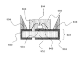
ここで、従来の白色LED光源の断面図を図5に示す(特許文献1参照)。図5において、LED501は基板507上に配置される。基板507は基材502上にLEDに電力を供給するための配線導体503がパターン形成されたものである。基材502としては絶縁性、耐熱性を持ったものが望まれ、素材として例えば、ガラスエポキシ、セラミックス、BTレジン、シリコンなどが用いられる。LED501は基板507上に実装する際に、ダイボンドペースト、Agペーストなどを使用して実装する。図5においてはダイボンドペースト504を用いて実装しているものとする。また、LED501と基板507の配線導体503はボンディングワイヤ505を用いて電気的に接続される。ボンディングワイヤ505としてはAu、Alなどが用いられる。LED501は配線導体503、ボンディングワイヤ505を介して外部より電力を供給され、発光するものである。
Here, sectional drawing of the conventional white LED light source is shown in FIG. 5 (refer patent document 1). In FIG. 5, the
また、LED501の周囲にはLED501を保護するための封止樹脂506を形成する。封止樹脂506としては透明性のあるエポキシ樹脂やシリコン樹脂が用いられる。また、封止樹脂506内には、LED501からの発光の一部を吸収し波長変換して発光する蛍光体やLED光源の光を均一にするための散乱材などが含まれる。また、封止樹脂506の外側には反射枠508を配置する。反射枠508はLED501からの発光を効率的に前面に照射させるためのものである。反射枠508は樹脂、セラミック、金属材料から成り、表面の反射率が高いものが用いられる。
A
ここで、LED501と蛍光体の組み合わせとしては、例えば特許文献1に記載されるように、LEDとして青色光を発光する窒化物系化合物半導体を用い、蛍光体としてセリウムで付活されたイットリウム・アルミニウム・ガーネット(YAG)系蛍光体を用いることにより、LED光源からの光線はLEDからの青色の発光と蛍光体からの波長変換された黄色の発光が混ざり合って白色光となることが広く知られている。また、LEDからの発光を紫外光とし、紫外光を吸収してRGBを発光する3種類の蛍光体を用いることでRGBが混ざり合って白色光とする方式も知られている。
Here, as a combination of the
このとき、封止樹脂506中に蛍光体を分散させる方式では、蛍光体が封止樹脂506内で一様に分散しない場合などはLED光源の発光に色むらが生じてしまうことが考えられる。そこで、例えば特許文献2によれば封止樹脂内のLED周辺部にのみ蛍光体と散乱材を配置することにより色むらを軽減する方法が挙げられている。
At this time, in the method in which the phosphor is dispersed in the sealing
しかし、前述の従来技術では以下に示す問題を有している。封止樹脂中に蛍光体を分散させ、LEDからの発光の一部を吸収し波長変換して発光させる場合、封止樹脂と蛍光体に大きな屈折率差が生じてしまう。例えば、シリコン樹脂は屈折率n=1.4程度であり、YAG系の蛍光体は屈折率n=1.82程度である。この場合、LEDからの発光は封止樹脂を通過し、屈折して蛍光体に入射するが、蛍光体からの発光が封止樹脂に出射する際は光線が屈折率の大きいところから小さいところ向かうため、臨界角以上の角度で蛍光体と封止樹脂の界面に到達した光線は全反射を起こしてしまう。上述の屈折率の例において、臨界角は約50度である。このとき、蛍光体内での光の吸収は0ではないため、全反射を繰り返すとそれだけ光量は低下してしまう。また、蛍光体は結晶構造を持つためその形状も規則性をもち、一度全反射を起こした光線は全反射を繰り返す可能性が高い。この場合、図6に示すように蛍光体601内で光線602が消光してしまうことも考えられる。上述の、LEDの周辺部に蛍光体を集中させた場合においても同様の現象はみられ、蛍光体内で光が吸収されてしまうことによりLED光源の光取り出し効率が低下してしまう。
However, the above-described conventional techniques have the following problems. When the phosphor is dispersed in the sealing resin and a part of the light emitted from the LED is absorbed and wavelength-converted to emit light, a large refractive index difference occurs between the sealing resin and the phosphor. For example, the refractive index n is about 1.4 for silicon resin, and the refractive index n is about 1.82 for YAG phosphor. In this case, the light emitted from the LED passes through the sealing resin, is refracted and enters the phosphor, but when the light emitted from the phosphor is emitted to the sealing resin, the light beam travels from a place where the refractive index is large to a place where it is small. Therefore, light rays that reach the interface between the phosphor and the sealing resin at an angle greater than the critical angle cause total reflection. In the refractive index example described above, the critical angle is about 50 degrees. At this time, since the light absorption in the phosphor is not zero, the amount of light decreases as the total reflection is repeated. In addition, since the phosphor has a crystal structure, the shape thereof is regular, and a light beam that has once undergone total reflection is highly likely to repeat total reflection. In this case, the
そこで、本発明では上述した従来技術による問題点を解消するため、蛍光体における光の吸収を低減し、LED光源の光取り出し効率を向上させることを目的とする。また、封止樹脂内での蛍光体の分布ばらつきによるLED光源における色むらを低減させることを目的とする。 Therefore, in order to eliminate the above-described problems caused by the prior art, an object of the present invention is to reduce light absorption in the phosphor and improve the light extraction efficiency of the LED light source. It is another object of the present invention to reduce color unevenness in an LED light source due to variation in phosphor distribution within the sealing resin.
これらの課題を解決するために本発明によるLED光源は、下記に記載の手段を採用する。すなわち本発明のLED光源は、LEDと、LEDからの発光の少なくとも一部を吸収し波長変換して発光する蛍光体と、LEDの周辺部に配置される封止樹脂とを有するLED光源であって、封止樹脂の外側にガラス層を有し、ガラス層は蛍光体と等しい屈折率を持つガラスの内部に蛍光体を分散したものであることを特徴とする。 In order to solve these problems, the LED light source according to the present invention employs the following means. That is, the LED light source of the present invention is an LED light source that includes an LED, a phosphor that absorbs at least a part of light emitted from the LED, converts the wavelength, and emits light, and a sealing resin disposed in the periphery of the LED. A glass layer is provided outside the sealing resin, and the glass layer is characterized in that the phosphor is dispersed in a glass having a refractive index equal to that of the phosphor.
また、本発明におけるガラス層は表面に微細構造を有することが好ましい。 Moreover, it is preferable that the glass layer in this invention has a fine structure on the surface.
また、本発明におけるガラス層は内部に散乱材が分散されていることが好ましい。 Moreover, it is preferable that the scattering material is disperse | distributed inside the glass layer in this invention.
また、本発明における封止樹脂は内部に散乱材が分散されていることが好ましい。 Moreover, it is preferable that the scattering material is disperse | distributed inside the sealing resin in this invention.
また、本発明における蛍光体はCeで付活されたYAG系の蛍光体であることが好ましい。 The phosphor in the present invention is preferably a YAG phosphor activated with Ce.
また、本発明におけるLEDは紫外光を発光し、蛍光体は青色光、緑色光、赤色光を発光する3種類の蛍光体からなることが好ましい。 The LED in the present invention preferably emits ultraviolet light, and the phosphor is preferably composed of three types of phosphors that emit blue light, green light, and red light.
また、本発明におけるガラスは低融点ガラスであることが好ましい。 Moreover, it is preferable that the glass in this invention is a low melting glass.
(作用)
LEDと、LEDからの発光の一部を吸収し波長変換して発光する蛍光体を有するLED光源において、蛍光体を蛍光体と同等の屈折率を持つガラスの内部に分散させたガラス層を封止樹脂の外側に配置することで、蛍光体とその周囲にある材料の屈折率差を低減させることができるため、蛍光体での発光が蛍光体内で吸収されてしまう現象を防ぐことが可能であり、LEDからの発光がLED光源内で吸収される割合を低減させることができるため、LED光源の光取り出し効率を向上させることが可能となる。
(Function)
In an LED light source having an LED and a phosphor that absorbs a part of light emitted from the LED and converts the wavelength to emit light, a glass layer in which the phosphor is dispersed inside a glass having a refractive index equivalent to that of the phosphor is sealed. By arranging it outside the stop resin, the refractive index difference between the phosphor and the surrounding material can be reduced, so it is possible to prevent the phenomenon that the phosphor emits light in the phosphor. In addition, since the rate at which the light emitted from the LED is absorbed in the LED light source can be reduced, the light extraction efficiency of the LED light source can be improved.
以上の説明のように、本発明のLED光源においては、下記に記載する効果を有する。 As described above, the LED light source of the present invention has the effects described below.
LEDと、LEDからの発光の一部を吸収し波長変換して発光する蛍光体を有するLED光源において、蛍光体を蛍光体と同等の屈折率を持つガラスの内部に分散させたガラス層を封止樹脂の外側に配置することで、蛍光体とその周囲にある材料の屈折率差を低減させることができるため、蛍光体での発光が蛍光体内で吸収されてしまう現象を防ぐことが可能である。また、ガラス層の表面に微細構造を設けることで、ガラス層から空気層へ光線が出射する際に全反射が起こるのを防ぐことができ、空気層へ光線が到達することができる。すなわち、LEDで発光した光線と、蛍光体がLEDからの発光の一部を吸収し波長変換して発光した光線が、LED光源内で吸収される割合を低減させることができるため、LED光源の光取り出し効率を向上させることが可能となる。 In an LED light source having an LED and a phosphor that absorbs a part of light emitted from the LED and converts the wavelength to emit light, a glass layer in which the phosphor is dispersed inside a glass having a refractive index equivalent to that of the phosphor is sealed. By arranging it outside the stop resin, the refractive index difference between the phosphor and the surrounding material can be reduced, so it is possible to prevent the phenomenon that the phosphor emits light in the phosphor. is there. Further, by providing a fine structure on the surface of the glass layer, it is possible to prevent total reflection from occurring when light rays are emitted from the glass layer to the air layer, and light rays can reach the air layer. That is, since the ratio of the light emitted from the LED and the light emitted from the phosphor by absorbing part of the light emitted from the LED and wavelength-converted can be reduced in the LED light source, The light extraction efficiency can be improved.
また更に、ガラス層の表面に微細構造を形成することにより、また、ガラス層もしくは封止樹脂内に散乱材を分散させることにより、光線を散乱させることができ、LEDからの発光と蛍光体からの発光もしくは異なる種類の蛍光体からの発光をより混ざり合った状態で出射することができるため、LED光源の色むらをより低減させることが可能である。 Furthermore, by forming a fine structure on the surface of the glass layer, or by dispersing a scattering material in the glass layer or the sealing resin, it is possible to scatter light rays, and from the light emission from the LED and the phosphor. Therefore, it is possible to emit light emitted from different types of phosphors in a more mixed state, so that the color unevenness of the LED light source can be further reduced.
以下、図面を用いて本発明を利用したLED光源の最適な実施形態を説明する。 Hereinafter, an optimum embodiment of an LED light source using the present invention will be described with reference to the drawings.
(第一の実施形態)
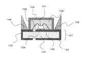
図1は本発明の第一の実施形態を示す図であり、本発明の第一の実施形態におけるLED光源の断面図である。また、図2は本発明の第一の実施形態におけるLED光源の断面図であり、ガラス層109付近の拡大図である。図1におけるLED光源において、LED101は基板107上に配置される。基板107は基材102上にLEDに電力を供給するための配線導体103がパターン形成されたものである。基材102としては絶縁性、耐熱性を持ったものが望まれ、素材として例えば、ガラスエポキシ、セラミックス、BTレジン、シリコンなどが用いられる。ここで、LED101からの発光は全方位に向かって起こるため、基材102としても反射率の高いものを使用することが望まれる。また、配線導体103は金属や導電ペーストを焼成したものであり、基材102と同様に反射率の高いことが望まれる。LED101は基板107上に実装する際に、ダイボンドペースト、Agペーストなどを使用して実装する。図1においては透明なダイボンドペースト104を用いて実装しているものとし、LED101からの後ろ方向への発光はダイボンドペースト104を透過し、基材102もしくは配線導体103で反射して前方向へ出射される。本実施形態においてはLED101からみて基板107側に出射する光線の方向を後ろ方向とする。
(First embodiment)
FIG. 1 is a diagram showing a first embodiment of the present invention, and is a cross-sectional view of an LED light source in the first embodiment of the present invention. FIG. 2 is a cross-sectional view of the LED light source in the first embodiment of the present invention, and is an enlarged view near the
また、LED101と基板107の配線導体103はボンディングワイヤ105を用いて電気的に接続される。ここで、ボンディングワイヤ105としてはAu、Alなどが用いられ、LED101上のパッドと配線導体103を接続するものである。LED101は配線導体103、ボンディングワイヤ105を介して外部より電力を供給され、発光するものである。ここで、本実施形態においては、LED101は窒化物系化合物半導体であり、青色を発光するものとする。
Further, the
また、LED101の周囲にはLED101を保護するための封止樹脂106を形成する。封止樹脂106としては透明性のあるエポキシ樹脂やシリコン樹脂が用いられる。また、封止樹脂106の外側には反射枠108を配置する。反射枠108はLED101か
らの発光を効率的に前面に照射させるためのものであり、樹脂、セラミック、金属材料など表面の反射率が高いものが用いられる。
A sealing
ここで、本実施形態においては封止樹脂106の周囲にガラス層109を配置する。このとき、ガラス層109は封止樹脂106と密着するものとする。ガラス層109はガラス202内に蛍光体201が分散されているもので、ガラス層109の厚みは数十〜数百μmである。ここで、蛍光体201はLED101からの青色の発光の一部を吸収し波長変換して黄色を発光するもので、本実施形態においてはセリウムで付活されたイットリウム・アルミニウム・ガーネット(YAG)系蛍光体であるものとする。また、ガラス202は蛍光体201の屈折率(n=1.82程度)とほぼ等しい値の屈折率を持ち、一般的なガラス(n=1.52)と比較して高屈折率のものである。また、ガラス層109の封止樹脂106と接しない面には微細構造203が設けられている。微細構造203は青色光もしくは黄色光の波長と比較して小さなピッチで凸凹が作成されているもので、ガラス202をエッチングするなどの方法で設けることが可能である。
Here, in this embodiment, the
ここで、LED101が発光した場合、LED101からの青色光はLED101の発光層から全方位に向かって発光する。このとき、LED101から後ろ方向に向かう光線は基板107で反射して、前面もしくは側面方向に向かうものである。LED101から前面もしくは側面方向に向かう光線は透明な封止樹脂106を通過し、ガラス層109に到達する。ここで、封止樹脂106とガラス層109の界面においては両者の屈折率が異なるため、界面に対して垂直入射する光線以外は屈折してガラス層109に入射する。ここで、封止樹脂106の屈折率はn=1.4程度であり、ガラス層109の屈折率はn=1.82程度であるため、光線は封止樹脂106からガラス層109に入射する際、屈折率のが低い領域から屈折率が高い領域へ光線が入射することになり、界面での全反射は起こらない。
Here, when the
次に、ガラス層109に入射した光線の一部はガラス層109内に分散した蛍光体201に到達する。蛍光体201に入射した青色光は蛍光体201に吸収され、波長変換されて黄色光が出射される。このとき、ガラス層109内における蛍光体201とガラス202は屈折率差がほとんどないため、蛍光体201内での発光は蛍光体201内で吸収されることなくガラス202に到達する。
Next, some of the light rays incident on the
ここで、一部が蛍光体201に吸収されたLED101からの青色光と蛍光体201からの黄色光はともにガラス層109の前面の空気との界面に到達する。このとき、ガラス層109から空気層に光線が出射する際、屈折率が高い領域から低い領域に光線が向かうため、界面が平坦な場合、ある角度以上で界面に入射した光線は全反射を起こし、空気層に光線が到達できない。本実施形態においては上述の通り、ガラス層109の封止樹脂106と接しない面には微細構造203が設けられており、微細構造203は青色光もしくは黄色光の波長と比較して小さなピッチで凸凹が作成されているので、界面において全反射は起こらず、光線が空気層に到達するものである。このとき、LED光源の使用者は青色光と黄色光が均一に混ざり合った光を白色光として認識することができ、白色LED光源としての使用が可能となる。また、微細構造203のピッチや高さを調整することで、界面において光線を散乱させることも可能で、より均一な白色光を出射することが可能となる。
Here, both the blue light from the
ここで、ガラス層109の厚みは数十μmから数百μmと薄いため、蛍光体201の分布の厚み方向へのばらつきを防ぐことができ蛍光体201をガラス層109内に均一に分散させることができる。そのため、ガラス層109の前面と空気層の界面においては、LED101からの青色光と蛍光体201からの黄色光を均一に混ぜ合わせることが可能で、色むらのない白色光が得られるものである。
Here, since the thickness of the
上述のように、LEDと、LEDからの発光の一部を吸収し波長変換して発光する蛍光体を有するLED光源において、蛍光体を蛍光体と同等の屈折率を持つガラスの内部に分散させたガラス層を封止樹脂の外側に配置することで、蛍光体とその周囲にある材料の屈折率差を低減させることができるため、蛍光体内で光が吸収されてしまう現象を防ぐことが可能である。また、ガラス層の表面に微細構造を設けることで、ガラス層から空気層へ光線が出射する際に全反射が起こるのを防ぐことができ、空気層へ光線が到達することができる。すなわち、LEDで発光した光線と、蛍光体がLEDからの発光の一部を吸収し波長変換して発光した光線が、LED光源内で吸収される割合を低減させることができるため、LED光源の光取り出し効率を向上させることが可能となる。 As described above, in an LED light source having an LED and a phosphor that absorbs a part of light emitted from the LED and converts the wavelength to emit light, the phosphor is dispersed inside a glass having a refractive index equivalent to that of the phosphor. By arranging the glass layer outside the sealing resin, the difference in refractive index between the phosphor and the surrounding material can be reduced, preventing the phenomenon that light is absorbed in the phosphor. It is. Further, by providing a fine structure on the surface of the glass layer, it is possible to prevent total reflection from occurring when light rays are emitted from the glass layer to the air layer, and light rays can reach the air layer. That is, since the ratio of the light emitted from the LED and the light emitted from the phosphor by absorbing part of the light emitted from the LED and wavelength-converted can be reduced in the LED light source, The light extraction efficiency can be improved.
更に、比較的薄いガラス層に蛍光体を分散させるため、深さ方向への蛍光体の分布ばらつきを抑制することができ、ガラス層に蛍光体を一様に分散させることが可能で、LED光源の色むらを低減することも可能となる。 Furthermore, since the phosphor is dispersed in a relatively thin glass layer, it is possible to suppress variation in the distribution of the phosphor in the depth direction, and to uniformly disperse the phosphor in the glass layer. It is also possible to reduce color unevenness.
上述の実施形態において、ガラス202に低融点ガラスを用いることにより、蛍光体201をガラス層109の内部に分散させる際に通常のガラスと比較して加熱する温度を下げることができ、蛍光体201へのダメージを与えることなく分散することができる。
In the above-described embodiment, by using a low-melting glass for the
(第二の実施形態)
次に第二の実施形態について説明する。図3は本発明の第二の実施形態におけるLED光源の断面図であり、ガラス層109付近の拡大図である。本実施形態におけるLED光源全体の断面図は図1の第一の実施形態と同様である。本実施形態においては、第一の実施形態と同様、図1におけるLED光源において、LED101は基板107上に配置される。基板107は基材102上にLEDに電力を供給するための配線導体103がパターン形成されたものである。LED101は基板107上に実装する際に、ダイボンドペースト、Agペーストなどを使用して実装する。図1においては透明なダイボンドペースト104を用いて実装しているものとする。本実施形態においても第一の実施形態と同様、LED101からみて基板107側に出射する光線の方向を後ろ方向とする。
(Second embodiment)
Next, a second embodiment will be described. FIG. 3 is a cross-sectional view of the LED light source in the second embodiment of the present invention, and is an enlarged view near the
また、LED101と基板107の配線導体103はボンディングワイヤ105を用いて電気的に接続される。LED101は配線導体103、ボンディングワイヤ105を介して外部より電力を供給され、発光するものである。ここで、本実施形態においては、LED101は窒化物系化合物半導体であり、青色を発光するものとする。また、LED101の周囲にはLED101を保護するための封止樹脂106を形成する。封止樹脂106としては透明性のあるエポキシ樹脂やシリコン樹脂が用いられる。また、封止樹脂106の外側には反射枠108を配置する。反射枠108はLED101からの発光を効率的に前面に照射させるためのものであり、樹脂、セラミック、金属材料など表面の反射率が高いものが用いられる。
Further, the
ここで、本実施形態においては封止樹脂106の周囲にガラス層109を配置する。このとき、ガラス層109は封止樹脂106と密着するものとする。図3に示すように、ガラス層109はガラス202内に蛍光体201と散乱材301が分散されているものである。ここで、蛍光体201はLED101からの青色の発光の一部を吸収し波長変換して黄色を発光するもので、本実施形態においても第一の実施形態と同様に、セリウムで付活されたYAG系蛍光体であるものとする。また、ガラス202は蛍光体201の屈折率(n=1.82程度)とほぼ等しい値の屈折率を持ち、一般的なガラス(n=1.52)と比較して高屈折率のものである。また、散乱材301はシリカなどを粉砕し微粒子化したものであり、散乱材301に入射した光線は散乱光となってランダムな方向に出射されるものである。また、ガラス層109の封止樹脂106と接しない面には微細構造203が
設けられている。微細構造203は青色光もしくは黄色光の波長と比較して小さなピッチで凸凹が作成されているもので、ガラス202をエッチングするなどの方法で設けることが可能である。
Here, in this embodiment, the
ここで、LED101が発光した場合、LED101からの青色光はLED101の発光層から全方位に向かって発光する。このとき、LED101から後ろ方向に向かう光線は基板107で反射して、前面もしくは側面方向に向かうものである。LED101から前面もしくは側面方向に向かう光線は透明な封止樹脂106を通過し、ガラス層109に到達する。ここで、封止樹脂106とガラス層109の界面においては両者の屈折率が異なるため、界面に対して垂直入射する光線以外は屈折してガラス層109に入射する。このとき、光線は屈折率の低い領域から屈折率が高い領域へ光線が入射することになり、界面での全反射は起こらない。
Here, when the
次に、ガラス層109に入射した光線の一部はガラス層109内に分散した蛍光体201もしくは散乱材301に到達する。蛍光体201に入射した青色光は蛍光体201に吸収され、波長変換されて黄色光が出射される。このとき、ガラス層109内における蛍光体201とガラス202は屈折率差がほとんどないため、蛍光体201内での発光は蛍光体201内で吸収されることなくガラス202に到達する。また、散乱材301に入射した光線は散乱光となってランダムな方向に出射されるものである。ここで、散乱材301はガラス層109内に一様に分布しているため、光線は散乱材301による散乱を繰り返し、その一部が蛍光体201に入射するため、一様な光線が蛍光体201に入射し波長変換されて出射される。
Next, part of the light rays incident on the
ここで、一部が蛍光体201に吸収されたLED101からの青色光と蛍光体201からの黄色光はともにガラス層109の前面の空気との界面に到達する。このとき、ガラス層109から空気層に光線が出射する際、屈折率が高い領域から低い領域に光線が向かうため、界面が平坦な場合、ある角度以上で界面に入射した光線は全反射を起こし、空気層に光線が到達できない。本実施形態においては上述の通り、ガラス層109の封止樹脂106と接しない面には微細構造203が設けられており、微細構造203は光の波長と比較して小さなピッチで凸凹が作成されているので、界面において全反射は起こらず、光線が空気層に到達するものである。このとき、LED光源の使用者は青色光と黄色光が均一に混ざり合った光を白色光として認識することができ、白色LED光源としての使用が可能となる。ここで、本実施形態においては散乱材301の影響によりLED光源からは青色光と黄色光がより混ざり合った状態で出射されるため、より色むらを低減することが可能である。
Here, both the blue light from the
上述のように、LEDと、LEDからの発光の一部を吸収し波長変換して発光する蛍光体を有するLED光源において、蛍光体と散乱材を蛍光体と同等の屈折率を持つガラスの内部に分散させたガラス層を封止樹脂の外側に配置することで、蛍光体とその周囲にある材料の屈折率差を低減させることができるため、蛍光体内で光が吸収されてしまう現象を防ぐことが可能である。また、ガラス層の表面に微細構造を設けることで、ガラス層から空気層へ光線が入射する際に全反射が起こるのを防ぐことができ、空気層へ光線が到達することができる。すなわち、LEDで発光した光線と、蛍光体がLEDからの発光の一部を吸収し波長変換して発光した光線が、LED光源内で吸収される割合を低減させることができるため、LED光源の光取り出し効率を向上させることが可能となる。更に、ガラス層に散乱材を分散させることにより、青色光と黄色光をより混ざり合った状態で出射することができるため、LED光源の色むらを低減することも可能となる。 As described above, in an LED light source having an LED and a phosphor that absorbs a part of light emitted from the LED and converts the wavelength to emit light, the phosphor and the scattering material are formed inside the glass having a refractive index equivalent to that of the phosphor. By disposing the glass layer dispersed in the outside of the sealing resin, the refractive index difference between the phosphor and the surrounding material can be reduced, thus preventing the phenomenon that light is absorbed in the phosphor. It is possible. Further, by providing a fine structure on the surface of the glass layer, it is possible to prevent total reflection from occurring when light rays are incident on the air layer from the glass layer, and light rays can reach the air layer. That is, since the ratio of the light emitted from the LED and the light emitted from the phosphor by absorbing part of the light emitted from the LED and wavelength-converted can be reduced in the LED light source, The light extraction efficiency can be improved. Furthermore, by dispersing the scattering material in the glass layer, it is possible to emit blue light and yellow light in a more mixed state, and thus it is possible to reduce color unevenness of the LED light source.
本実施形態においては、散乱材301をガラス層109内に分散させて、LED光源の色むらを低減させているが、散乱材301を封止樹脂106内に分散させて、散乱した光
線をガラス層109に到達させた場合でも同様の効果が得られるものである。
In this embodiment, the
上述の実施形態においては、封止樹脂106と反射枠108が接していない形態となっているが、これに限るものではなく、図4に示すように反射枠108と封止樹脂106が密着しており、前面にのみガラス層109を配置する構成としても同様の効果が得られるものである。
In the above-described embodiment, the sealing
また、上述の実施形態においては、ガラス層109の封止樹脂106と接しない面にのみ微細構造203を設けているが、それに加えてガラス層109の封止樹脂106と接する面にも微細構造を設けることによって、光線が封止樹脂106からガラス層109に入射する際の反射を抑制させることができ、LED光源の光取り出し効率を向上させることが可能である。
In the above-described embodiment, the
また、上述の実施形態においては、LED101と蛍光体201の組み合わせとして、青色光を発光する窒化物系化合物半導体とセリウムで付活されたYAG系蛍光体を用いているが、これに限るものではなく、青色光を発光するその他のLEDや青色光を吸収して波長変換して発光するその他の蛍光体を用いることも可能である。また、紫外光を発光するLEDを用い、紫外光を吸収してRGBを発光する3種類の蛍光体を用いることも可能である。
In the above-described embodiment, a nitride compound semiconductor emitting blue light and a YAG phosphor activated with cerium are used as a combination of the
また、上述の実施形態においては、ボンディングワイヤを用いる実装としているが、これに限るものではなく、フリップチップタイプのLEDを実装したLED光源においても同様の効果が得られるものである。 In the above-described embodiment, the mounting using the bonding wire is used. However, the present invention is not limited to this, and the same effect can be obtained in an LED light source on which a flip-chip type LED is mounted.
上述の実施形態において、LEDとは半導体発光素子を指し、LED光源とはLEDが実装された基板等を含む電子部品のことを指すものとする。 In the above-described embodiments, the LED refers to a semiconductor light emitting element, and the LED light source refers to an electronic component including a substrate on which the LED is mounted.
101 LED
102 基材
103 配線導体
105 ボンディングワイヤ
106 封止樹脂
107 基板
108 反射枠
109 ガラス層
201 蛍光体
202 ガラス
203 微細構造
301 散乱材
101 LED
102
Claims (7)
Priority Applications (1)
| Application Number | Priority Date | Filing Date | Title |
|---|---|---|---|
| JP2007235257A JP2009070892A (en) | 2007-09-11 | 2007-09-11 | Led light source |
Applications Claiming Priority (1)
| Application Number | Priority Date | Filing Date | Title |
|---|---|---|---|
| JP2007235257A JP2009070892A (en) | 2007-09-11 | 2007-09-11 | Led light source |
Publications (1)
| Publication Number | Publication Date |
|---|---|
| JP2009070892A true JP2009070892A (en) | 2009-04-02 |
Family
ID=40606868
Family Applications (1)
| Application Number | Title | Priority Date | Filing Date |
|---|---|---|---|
| JP2007235257A Pending JP2009070892A (en) | 2007-09-11 | 2007-09-11 | Led light source |
Country Status (1)
| Country | Link |
|---|---|
| JP (1) | JP2009070892A (en) |
Cited By (8)
| Publication number | Priority date | Publication date | Assignee | Title |
|---|---|---|---|---|
| JP2011222751A (en) * | 2010-04-09 | 2011-11-04 | Nippon Electric Glass Co Ltd | Wavelength conversion member and semiconductor light-emitting element device having and using the wavelength conversion member |
| JP2013514656A (en) * | 2009-12-17 | 2013-04-25 | コーニンクレッカ フィリップス エレクトロニクス エヌ ヴィ | Illumination device including light source and wavelength conversion component |
| JP2014500214A (en) * | 2010-10-28 | 2014-01-09 | コーニング インコーポレイテッド | Phosphor-containing glass frit material for LED lighting applications |
| JP2015130459A (en) * | 2014-01-09 | 2015-07-16 | 電気化学工業株式会社 | Phosphor-containing multilayer film sheet and light-emitting device |
| JP5998481B2 (en) * | 2010-11-12 | 2016-09-28 | 三菱マテリアル株式会社 | Method for manufacturing light emitting device |
| JP2016186974A (en) * | 2015-03-27 | 2016-10-27 | 東レエンジニアリング株式会社 | Led module and led module manufacturing method |
| US9944849B2 (en) | 2009-12-17 | 2018-04-17 | Koninklijke Philips N.V. | Light emitting diode device with luminescent material |
| US10158057B2 (en) | 2010-10-28 | 2018-12-18 | Corning Incorporated | LED lighting devices |
-
2007
- 2007-09-11 JP JP2007235257A patent/JP2009070892A/en active Pending
Cited By (10)
| Publication number | Priority date | Publication date | Assignee | Title |
|---|---|---|---|---|
| JP2013514656A (en) * | 2009-12-17 | 2013-04-25 | コーニンクレッカ フィリップス エレクトロニクス エヌ ヴィ | Illumination device including light source and wavelength conversion component |
| US9175214B2 (en) | 2009-12-17 | 2015-11-03 | Koninklijke Philips N.V. | Lighting device with light source and wavelength converting element |
| US9944849B2 (en) | 2009-12-17 | 2018-04-17 | Koninklijke Philips N.V. | Light emitting diode device with luminescent material |
| JP2011222751A (en) * | 2010-04-09 | 2011-11-04 | Nippon Electric Glass Co Ltd | Wavelength conversion member and semiconductor light-emitting element device having and using the wavelength conversion member |
| JP2014500214A (en) * | 2010-10-28 | 2014-01-09 | コーニング インコーポレイテッド | Phosphor-containing glass frit material for LED lighting applications |
| US10158057B2 (en) | 2010-10-28 | 2018-12-18 | Corning Incorporated | LED lighting devices |
| JP5998481B2 (en) * | 2010-11-12 | 2016-09-28 | 三菱マテリアル株式会社 | Method for manufacturing light emitting device |
| US9647185B2 (en) | 2010-11-12 | 2017-05-09 | Mitsubishi Materials Corporation | Composition for reflection film for light emitting element, light emitting element, and method of producing light emitting element |
| JP2015130459A (en) * | 2014-01-09 | 2015-07-16 | 電気化学工業株式会社 | Phosphor-containing multilayer film sheet and light-emitting device |
| JP2016186974A (en) * | 2015-03-27 | 2016-10-27 | 東レエンジニアリング株式会社 | Led module and led module manufacturing method |
Similar Documents
| Publication | Publication Date | Title |
|---|---|---|
| JP5307881B2 (en) | Semiconductor light emitting device | |
| JP5521325B2 (en) | Light emitting device and manufacturing method thereof | |
| JP5515992B2 (en) | Light emitting device | |
| JP5557828B2 (en) | Light emitting device | |
| US8723409B2 (en) | Light emitting device | |
| JP5810301B2 (en) | Lighting device | |
| WO2014122888A1 (en) | Light-emitting module | |
| JP2010283281A (en) | Light emitting device | |
| JP2009070892A (en) | Led light source | |
| US9537062B2 (en) | Solid state light emitter package, a light emission device, a flexible LED strip and a luminaire | |
| JP6457225B2 (en) | Light emitting device | |
| JP2017162942A (en) | Light-emitting device and illuminating device | |
| JP2005109289A (en) | Light-emitting device | |
| US11512817B2 (en) | Automotive LED light source with glass lens over a glass converter plate containing phosphor | |
| JP2011171504A (en) | Light-emitting device | |
| JP2005332951A (en) | Light emitting device | |
| JP6997869B2 (en) | Wavelength conversion element and light source device | |
| JP5786278B2 (en) | Light emitting device | |
| JP5644967B2 (en) | Light emitting device and manufacturing method thereof | |
| JP2017054994A (en) | Light emitting device and luminaire | |
| JP5678462B2 (en) | Light emitting device | |
| JP2008166311A (en) | Semiconductor light-emitting element and semiconductor light-emitting device | |
| KR100712880B1 (en) | White light emitting diode capable of reducing correlated color temperature variation | |
| JP2017163002A (en) | Light-emitting device and illuminating device | |
| JP2018156966A (en) | Light-emitting device and illumination device |