JP2009070840A - Semiconductor device and manufacturing method thereof - Google Patents
Semiconductor device and manufacturing method thereof Download PDFInfo
- Publication number
- JP2009070840A JP2009070840A JP2007234173A JP2007234173A JP2009070840A JP 2009070840 A JP2009070840 A JP 2009070840A JP 2007234173 A JP2007234173 A JP 2007234173A JP 2007234173 A JP2007234173 A JP 2007234173A JP 2009070840 A JP2009070840 A JP 2009070840A
- Authority
- JP
- Japan
- Prior art keywords
- film
- impurity
- doped
- amorphous silicon
- semiconductor device
- Prior art date
- Legal status (The legal status is an assumption and is not a legal conclusion. Google has not performed a legal analysis and makes no representation as to the accuracy of the status listed.)
- Abandoned
Links
- 239000004065 semiconductor Substances 0.000 title claims abstract description 53
- 238000004519 manufacturing process Methods 0.000 title claims description 40
- 239000012535 impurity Substances 0.000 claims abstract description 133
- 229910021420 polycrystalline silicon Inorganic materials 0.000 claims abstract description 105
- 229920005591 polysilicon Polymers 0.000 claims abstract description 105
- 229910052751 metal Inorganic materials 0.000 claims abstract description 35
- 239000002184 metal Substances 0.000 claims abstract description 35
- 229910021332 silicide Inorganic materials 0.000 claims abstract description 35
- FVBUAEGBCNSCDD-UHFFFAOYSA-N silicide(4-) Chemical compound [Si-4] FVBUAEGBCNSCDD-UHFFFAOYSA-N 0.000 claims abstract description 35
- ZOXJGFHDIHLPTG-UHFFFAOYSA-N Boron Chemical compound [B] ZOXJGFHDIHLPTG-UHFFFAOYSA-N 0.000 claims abstract description 33
- 229910052796 boron Inorganic materials 0.000 claims abstract description 33
- 238000011068 loading method Methods 0.000 claims abstract description 3
- 229910021417 amorphous silicon Inorganic materials 0.000 claims description 94
- 238000000034 method Methods 0.000 claims description 33
- OAICVXFJPJFONN-UHFFFAOYSA-N Phosphorus Chemical group [P] OAICVXFJPJFONN-UHFFFAOYSA-N 0.000 claims description 28
- 229910052698 phosphorus Inorganic materials 0.000 claims description 28
- 239000011574 phosphorus Substances 0.000 claims description 28
- 238000005468 ion implantation Methods 0.000 claims description 24
- 238000009792 diffusion process Methods 0.000 claims description 22
- XUIMIQQOPSSXEZ-UHFFFAOYSA-N Silicon Chemical compound [Si] XUIMIQQOPSSXEZ-UHFFFAOYSA-N 0.000 claims description 21
- 229910052710 silicon Inorganic materials 0.000 claims description 21
- 239000010703 silicon Substances 0.000 claims description 21
- 239000000758 substrate Substances 0.000 claims description 19
- 238000010521 absorption reaction Methods 0.000 abstract description 8
- 230000035515 penetration Effects 0.000 abstract description 7
- 239000010410 layer Substances 0.000 description 28
- 239000007789 gas Substances 0.000 description 12
- 229910052721 tungsten Inorganic materials 0.000 description 9
- 239000010937 tungsten Substances 0.000 description 9
- 230000015572 biosynthetic process Effects 0.000 description 6
- 230000009977 dual effect Effects 0.000 description 6
- WQJQOUPTWCFRMM-UHFFFAOYSA-N tungsten disilicide Chemical compound [Si]#[W]#[Si] WQJQOUPTWCFRMM-UHFFFAOYSA-N 0.000 description 6
- 229910021342 tungsten silicide Inorganic materials 0.000 description 6
- VYPSYNLAJGMNEJ-UHFFFAOYSA-N Silicium dioxide Chemical compound O=[Si]=O VYPSYNLAJGMNEJ-UHFFFAOYSA-N 0.000 description 5
- 229910052814 silicon oxide Inorganic materials 0.000 description 5
- WFKWXMTUELFFGS-UHFFFAOYSA-N tungsten Chemical compound [W] WFKWXMTUELFFGS-UHFFFAOYSA-N 0.000 description 5
- 230000000694 effects Effects 0.000 description 4
- -1 tungsten nitride Chemical class 0.000 description 4
- BLRPTPMANUNPDV-UHFFFAOYSA-N Silane Chemical compound [SiH4] BLRPTPMANUNPDV-UHFFFAOYSA-N 0.000 description 3
- 239000002019 doping agent Substances 0.000 description 3
- 230000000149 penetrating effect Effects 0.000 description 3
- 229910000077 silane Inorganic materials 0.000 description 3
- WNUPENMBHHEARK-UHFFFAOYSA-N silicon tungsten Chemical compound [Si].[W] WNUPENMBHHEARK-UHFFFAOYSA-N 0.000 description 3
- IJGRMHOSHXDMSA-UHFFFAOYSA-N Atomic nitrogen Chemical compound N#N IJGRMHOSHXDMSA-UHFFFAOYSA-N 0.000 description 2
- 238000010438 heat treatment Methods 0.000 description 2
- 238000002513 implantation Methods 0.000 description 2
- 150000002500 ions Chemical class 0.000 description 2
- 238000002955 isolation Methods 0.000 description 2
- 230000000873 masking effect Effects 0.000 description 2
- 238000004544 sputter deposition Methods 0.000 description 2
- 229910004298 SiO 2 Inorganic materials 0.000 description 1
- 230000003213 activating effect Effects 0.000 description 1
- 238000000137 annealing Methods 0.000 description 1
- 229910052785 arsenic Inorganic materials 0.000 description 1
- RQNWIZPPADIBDY-UHFFFAOYSA-N arsenic atom Chemical compound [As] RQNWIZPPADIBDY-UHFFFAOYSA-N 0.000 description 1
- IVHJCRXBQPGLOV-UHFFFAOYSA-N azanylidynetungsten Chemical compound [W]#N IVHJCRXBQPGLOV-UHFFFAOYSA-N 0.000 description 1
- 230000004888 barrier function Effects 0.000 description 1
- 238000010009 beating Methods 0.000 description 1
- 238000005229 chemical vapour deposition Methods 0.000 description 1
- 238000007796 conventional method Methods 0.000 description 1
- 238000002425 crystallisation Methods 0.000 description 1
- 230000008025 crystallization Effects 0.000 description 1
- 230000006866 deterioration Effects 0.000 description 1
- MROCJMGDEKINLD-UHFFFAOYSA-N dichlorosilane Chemical compound Cl[SiH2]Cl MROCJMGDEKINLD-UHFFFAOYSA-N 0.000 description 1
- OKZIUSOJQLYFSE-UHFFFAOYSA-N difluoroboron Chemical compound F[B]F OKZIUSOJQLYFSE-UHFFFAOYSA-N 0.000 description 1
- 238000005530 etching Methods 0.000 description 1
- 238000011065 in-situ storage Methods 0.000 description 1
- 238000002347 injection Methods 0.000 description 1
- 239000007924 injection Substances 0.000 description 1
- 238000012986 modification Methods 0.000 description 1
- 230000004048 modification Effects 0.000 description 1
- 229910052757 nitrogen Inorganic materials 0.000 description 1
- 230000003647 oxidation Effects 0.000 description 1
- 238000007254 oxidation reaction Methods 0.000 description 1
- 230000001590 oxidative effect Effects 0.000 description 1
- 238000000059 patterning Methods 0.000 description 1
- 238000000206 photolithography Methods 0.000 description 1
- 230000001846 repelling effect Effects 0.000 description 1
- 239000002356 single layer Substances 0.000 description 1
- NXHILIPIEUBEPD-UHFFFAOYSA-H tungsten hexafluoride Chemical compound F[W](F)(F)(F)(F)F NXHILIPIEUBEPD-UHFFFAOYSA-H 0.000 description 1
Images


Classifications
-
- H—ELECTRICITY
- H01—ELECTRIC ELEMENTS
- H01L—SEMICONDUCTOR DEVICES NOT COVERED BY CLASS H10
- H01L21/00—Processes or apparatus adapted for the manufacture or treatment of semiconductor or solid state devices or of parts thereof
- H01L21/70—Manufacture or treatment of devices consisting of a plurality of solid state components formed in or on a common substrate or of parts thereof; Manufacture of integrated circuit devices or of parts thereof
- H01L21/77—Manufacture or treatment of devices consisting of a plurality of solid state components or integrated circuits formed in, or on, a common substrate
- H01L21/78—Manufacture or treatment of devices consisting of a plurality of solid state components or integrated circuits formed in, or on, a common substrate with subsequent division of the substrate into plural individual devices
- H01L21/82—Manufacture or treatment of devices consisting of a plurality of solid state components or integrated circuits formed in, or on, a common substrate with subsequent division of the substrate into plural individual devices to produce devices, e.g. integrated circuits, each consisting of a plurality of components
- H01L21/822—Manufacture or treatment of devices consisting of a plurality of solid state components or integrated circuits formed in, or on, a common substrate with subsequent division of the substrate into plural individual devices to produce devices, e.g. integrated circuits, each consisting of a plurality of components the substrate being a semiconductor, using silicon technology
- H01L21/8232—Field-effect technology
- H01L21/8234—MIS technology, i.e. integration processes of field effect transistors of the conductor-insulator-semiconductor type
- H01L21/8238—Complementary field-effect transistors, e.g. CMOS
- H01L21/823828—Complementary field-effect transistors, e.g. CMOS with a particular manufacturing method of the gate conductors, e.g. particular materials, shapes
- H01L21/823842—Complementary field-effect transistors, e.g. CMOS with a particular manufacturing method of the gate conductors, e.g. particular materials, shapes gate conductors with different gate conductor materials or different gate conductor implants, e.g. dual gate structures
-
- H—ELECTRICITY
- H01—ELECTRIC ELEMENTS
- H01L—SEMICONDUCTOR DEVICES NOT COVERED BY CLASS H10
- H01L21/00—Processes or apparatus adapted for the manufacture or treatment of semiconductor or solid state devices or of parts thereof
- H01L21/02—Manufacture or treatment of semiconductor devices or of parts thereof
- H01L21/04—Manufacture or treatment of semiconductor devices or of parts thereof the devices having at least one potential-jump barrier or surface barrier, e.g. PN junction, depletion layer or carrier concentration layer
- H01L21/18—Manufacture or treatment of semiconductor devices or of parts thereof the devices having at least one potential-jump barrier or surface barrier, e.g. PN junction, depletion layer or carrier concentration layer the devices having semiconductor bodies comprising elements of Group IV of the Periodic System or AIIIBV compounds with or without impurities, e.g. doping materials
- H01L21/28—Manufacture of electrodes on semiconductor bodies using processes or apparatus not provided for in groups H01L21/20 - H01L21/268
- H01L21/28008—Making conductor-insulator-semiconductor electrodes
- H01L21/28017—Making conductor-insulator-semiconductor electrodes the insulator being formed after the semiconductor body, the semiconductor being silicon
- H01L21/28026—Making conductor-insulator-semiconductor electrodes the insulator being formed after the semiconductor body, the semiconductor being silicon characterised by the conductor
- H01L21/28035—Making conductor-insulator-semiconductor electrodes the insulator being formed after the semiconductor body, the semiconductor being silicon characterised by the conductor the final conductor layer next to the insulator being silicon, e.g. polysilicon, with or without impurities
- H01L21/28044—Making conductor-insulator-semiconductor electrodes the insulator being formed after the semiconductor body, the semiconductor being silicon characterised by the conductor the final conductor layer next to the insulator being silicon, e.g. polysilicon, with or without impurities the conductor comprising at least another non-silicon conductive layer
- H01L21/28052—Making conductor-insulator-semiconductor electrodes the insulator being formed after the semiconductor body, the semiconductor being silicon characterised by the conductor the final conductor layer next to the insulator being silicon, e.g. polysilicon, with or without impurities the conductor comprising at least another non-silicon conductive layer the conductor comprising a silicide layer formed by the silicidation reaction of silicon with a metal layer
-
- H—ELECTRICITY
- H01—ELECTRIC ELEMENTS
- H01L—SEMICONDUCTOR DEVICES NOT COVERED BY CLASS H10
- H01L29/00—Semiconductor devices adapted for rectifying, amplifying, oscillating or switching, or capacitors or resistors with at least one potential-jump barrier or surface barrier, e.g. PN junction depletion layer or carrier concentration layer; Details of semiconductor bodies or of electrodes thereof ; Multistep manufacturing processes therefor
- H01L29/40—Electrodes ; Multistep manufacturing processes therefor
- H01L29/43—Electrodes ; Multistep manufacturing processes therefor characterised by the materials of which they are formed
- H01L29/49—Metal-insulator-semiconductor electrodes, e.g. gates of MOSFET
- H01L29/4916—Metal-insulator-semiconductor electrodes, e.g. gates of MOSFET the conductor material next to the insulator being a silicon layer, e.g. polysilicon doped with boron, phosphorus or nitrogen
- H01L29/4925—Metal-insulator-semiconductor electrodes, e.g. gates of MOSFET the conductor material next to the insulator being a silicon layer, e.g. polysilicon doped with boron, phosphorus or nitrogen with a multiple layer structure, e.g. several silicon layers with different crystal structure or grain arrangement
- H01L29/4941—Metal-insulator-semiconductor electrodes, e.g. gates of MOSFET the conductor material next to the insulator being a silicon layer, e.g. polysilicon doped with boron, phosphorus or nitrogen with a multiple layer structure, e.g. several silicon layers with different crystal structure or grain arrangement with a barrier layer between the silicon and the metal or metal silicide upper layer, e.g. Silicide/TiN/Polysilicon
Abstract
Description
本発明は、半導体装置及びその製造方法に関し、特に、多層構造のシリコンゲートを備えた半導体装置及びその製造方法に関するものである。 The present invention relates to a semiconductor device and a manufacturing method thereof, and more particularly to a semiconductor device including a multi-layered silicon gate and a manufacturing method thereof.
近年、デュアルゲート構造のCMOSが注目されている。通常のCMOSでは、n+ポリシリコン膜上に金属シリサイド膜を積層したポリメタルゲートをNMOSFETとPMOSFETの両方で使用するシングルゲート構造が採用されている。シングルゲート構造はシンプルなプロセスで実現できるが、PMOSFETにおいて短チャネル効果が発生しやすいため、微細なデバイスの実現は困難である。 In recent years, a CMOS having a dual gate structure has attracted attention. A normal CMOS employs a single gate structure in which a polymetal gate in which a metal silicide film is stacked on an n + polysilicon film is used in both an NMOSFET and a PMOSFET. The single gate structure can be realized by a simple process, but since a short channel effect is likely to occur in the PMOSFET, it is difficult to realize a fine device.
これに対し、デュアルゲート構造のCMOSでは、n+ポリシリコンと金属シリサイドを積層したポリメタルゲートをNMOSFETに用い、p+ポリシリコンと金属シリサイドを積層したポリメタルゲートをPMOSFETに用いる。そのため、短チャネル効果が小さく駆動力の大きなCMOSを実現することができる。 On the other hand, in a dual gate CMOS, a polymetal gate in which n + polysilicon and metal silicide are stacked is used for an NMOSFET, and a polymetal gate in which p + polysilicon and metal silicide are stacked is used for a PMOSFET. Therefore, a CMOS having a small short channel effect and a large driving force can be realized.
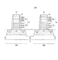
図13は、デュアルゲート構造を有する従来の半導体装置の製造工程の一部を示す略断面図である。 FIG. 13 is a schematic sectional view showing a part of a manufacturing process of a conventional semiconductor device having a dual gate structure.
図13に示すように、デュアルゲートの形成では、まずシリコン基板51上にSiONからなるゲート絶縁膜52を形成した後、ゲート電極用のノンドープドアモルファスシリコン膜53を形成する。次に、ノンドープドアモルファスシリコン膜53にp型不純物又はn型不純物を導入する。このとき、NMOSであればリン(P)、ヒ素(As)等のn型不純物をイオン注入し、PMOSであればホウ素(B)、二フッ化ホウ素(BF2)等のp型不純物をイオン注入する。つまり、ゲート電極の導電型に応じたドーパントの打ち分けが行われる。その後、タングステンシリサイド(WSi)等の金属シリサイド膜54を形成し、さらに不純物を活性化させるためのアニール等の高温熱負荷工程を行って、アモルファスシリコン膜53中にドーパントを拡散させている。
As shown in FIG. 13, in forming a dual gate, a
ところで、上述した従来の半導体装置の製造方法においては、PMOSFETの形成領域のアモルファスシリコン膜53中にドーピングしたホウ素(B)が高温熱負荷の際にゲート絶縁膜52を突き抜けてシリコン基板51にまで達する、いわゆるホウ素突き抜けの問題が発生することが知られている。ホウ素の突き抜けが生じると、PMOSFETの閾値電圧(Vth)が大きく変動してしまい、トランジスタ特性が劣化するという問題がある。
By the way, in the above-described conventional method for manufacturing a semiconductor device, boron (B) doped in the
ホウ素突き抜けの問題を解決するため、例えば特許文献1においては、NMOSFET及びPMOSFETの各ゲート電極のポリシリコンにp+不純物を導入し、p+シングルゲートを採用すると共に、ゲート絶縁膜が、窒素を最大濃度領域にて1×10²⁰/cm3以上1×1022/cm3以下の範囲で含む窒化酸化膜(SiON)で形成されたCMOSFETが提案されている。
上述したように、従来の半導体装置の製造においては、ホウ素(B)がゲート絶縁膜を突き抜けることによる閾値電圧(Vth)のばらつきを生じさせるという問題がある。また、高温熱処理の際、金属シリサイド膜がポリシリコン膜中の不純物を吸収することや、ポリシリコン膜外への不純物流出によって、ポリシリコン膜中の不純物の空乏化が引き起こされ、トランジスタ特性が低下するという問題もある。 As described above, in the manufacture of a conventional semiconductor device, there is a problem in that the threshold voltage (Vth) varies due to boron (B) penetrating through the gate insulating film. Also, during high-temperature heat treatment, the metal silicide film absorbs impurities in the polysilicon film, and impurity outflow from the polysilicon film causes depletion of impurities in the polysilicon film, resulting in deterioration of transistor characteristics. There is also the problem of doing.
したがって、本発明の目的は、ポリシリコン膜中の不純物濃度プロファイルが良好であり、閾値電圧のばらつきが抑制された高性能な半導体装置を提供することにある。 Accordingly, an object of the present invention is to provide a high-performance semiconductor device in which the impurity concentration profile in the polysilicon film is good and the variation in threshold voltage is suppressed.
また、本発明の目的は、ホウ素(B)のゲート絶縁膜の突き抜けや金属シリサイド膜による不純物の吸収によって生じるポリシリコン膜中の不純物の空乏化を防止することが可能な半導体装置の製造方法を提供することにある。 Another object of the present invention is to provide a method of manufacturing a semiconductor device capable of preventing the depletion of impurities in a polysilicon film caused by penetration of a boron (B) gate insulating film or absorption of impurities by a metal silicide film. It is to provide.
本発明の上記目的は、シリコン基板上と、シリコン基板上に形成されたゲート絶縁膜と、ゲート絶縁膜上に形成されたゲート電極とを備え、ゲート電極は、ゲート絶縁膜上に形成された第1のドープドポリシリコン膜と、第1のドープドポリシリコン膜上に形成された第2のドープドポリシリコン膜とを備え、第1のドープドポリシリコン膜は、第1の不純物を含み、第2のドープドポリシリコン膜は、第1の不純物とは反対の導電型を有する第2の不純物を含むことを特徴とする半導体装置によって達成される。 The object of the present invention includes a silicon substrate, a gate insulating film formed on the silicon substrate, and a gate electrode formed on the gate insulating film, and the gate electrode is formed on the gate insulating film. A first doped polysilicon film; and a second doped polysilicon film formed on the first doped polysilicon film. The first doped polysilicon film contains a first impurity. The second doped polysilicon film is achieved by a semiconductor device including a second impurity having a conductivity type opposite to that of the first impurity.
本発明によれば、第2のドープドポリシリコン膜とゲート絶縁膜との間に第1のドープドポリシリコン膜が介在しており、第1ドープドポリシリコン膜中の不純物と第2のドープドポリシリコン膜中の不純物の導電型が異なることから、ポリシリコン中の不純物の拡散工程やその後の高温熱負荷工程において、第2のドープドポリシリコン膜中の不純物の過度な拡散が抑制される。したがって、不純物がゲート絶縁膜の突き抜けることによって生じるVthのばらつきやポリシリコン膜中の不純物の空乏化を防止することができる。 According to the present invention, the first doped polysilicon film is interposed between the second doped polysilicon film and the gate insulating film, and the impurities in the first doped polysilicon film and the second Since the conductivity type of the impurities in the doped polysilicon film is different, excessive diffusion of impurities in the second doped polysilicon film is suppressed in the impurity diffusion process in the polysilicon and the subsequent high-temperature heat load process. Is done. Therefore, it is possible to prevent variations in Vth caused by impurities penetrating through the gate insulating film and depletion of impurities in the polysilicon film.
本発明において、ゲート電極は、第2のドープドポリシリコン膜上に形成された第3のドープドポリシリコン膜をさらに備え、第3のドープドポリシリコン膜は、第1の不純物を含むことが好ましい。また、ゲート電極は、第3のドープドポリシリコン膜上に形成された金属シリサイド膜をさらに備えることが好ましい。 In the present invention, the gate electrode further includes a third doped polysilicon film formed on the second doped polysilicon film, and the third doped polysilicon film contains the first impurity. Is preferred. The gate electrode preferably further includes a metal silicide film formed on the third doped polysilicon film.
ゲート電極が金属シリサイドを含む場合には、ポリシリコン中の不純物の拡散工程やその後の高温熱負荷工程において、金属シリサイド膜が不純物を吸収し、ポリシリコン膜中の不純物の空乏化を生じさせるが、第2のポリシリコン膜と金属シリサイド膜との間に第3のドープドポリシリコン膜が介在している場合には、第2のドープドポリシリコン膜中の不純物の過度な拡散を抑制することができ、金属シリサイド膜が不純物を吸収することによるポリシリコン膜中の不純物の空乏化を防止することができる。 When the gate electrode contains metal silicide, the metal silicide film absorbs impurities in the diffusion process of impurities in the polysilicon and the subsequent high-temperature heat load process, which causes depletion of impurities in the polysilicon film. In the case where the third doped polysilicon film is interposed between the second polysilicon film and the metal silicide film, excessive diffusion of impurities in the second doped polysilicon film is suppressed. In addition, depletion of impurities in the polysilicon film due to absorption of impurities by the metal silicide film can be prevented.
本発明において、第1及び第3のドープドポリシリコン膜中の第1の不純物の濃度は、第2のドープドポリシリコン膜中の第2の不純物の濃度よりも低いことが好ましい。また、第1及び第3のドープドポリシリコン膜は、第2の不純物をさらに含み、第1及び第3のドープドポリシリコン膜中の第2の不純物の濃度は、第2のドープドポリシリコン膜中の第2の不純物の濃度よりも低いことが好ましい。1乃至第3のドープドポリシリコン膜中の不純物濃度が以上のような関係を有していれば、特性の良好なポリシリコンゲートを構成することができる。 In the present invention, the concentration of the first impurity in the first and third doped polysilicon films is preferably lower than the concentration of the second impurity in the second doped polysilicon film. The first and third doped polysilicon films further include a second impurity, and the concentration of the second impurity in the first and third doped polysilicon films is the second doped polysilicon film. The concentration is preferably lower than the concentration of the second impurity in the silicon film. If the impurity concentrations in the first to third doped polysilicon films have the above relationship, a polysilicon gate with good characteristics can be configured.
なお、本発明においては、第1の不純物がリン(P)であり、第2の不純物がホウ素(B)であることが好ましい。第2の不純物としてホウ素(B)を用いた場合には、熱負荷工程において不純物のゲート絶縁膜突き抜けの問題が顕著に現れ、本発明の効果も顕著となるからである。また、第1の不純物としてリン(P)を用いた場合には、熱負荷工程におけるリン(P)自体の拡散が特に酸化膜中で起こり難く、しかもホウ素(B)の過度な拡散を阻止する効果を有し、ホウ素(B)のゲート絶縁膜突き抜けを防止できるからである。 In the present invention, it is preferable that the first impurity is phosphorus (P) and the second impurity is boron (B). This is because when boron (B) is used as the second impurity, the problem of the penetration of the impurity into the gate insulating film appears remarkably in the heat load step, and the effect of the present invention becomes remarkable. Further, when phosphorus (P) is used as the first impurity, the diffusion of phosphorus (P) itself in the heat load process is difficult to occur particularly in the oxide film, and the excessive diffusion of boron (B) is prevented. This is because it has an effect and can prevent boron (B) from penetrating through the gate insulating film.
本発明の上記目的はまた、シリコン基板上にゲート絶縁膜を形成するゲート絶縁膜形成工程と、ゲート絶縁膜上にゲート電極を形成するゲート電極形成工程と、シリコン基板全体に熱負荷を加える熱負荷工程とを備え、ゲート電極形成工程は、ゲート絶縁膜上に第1の不純物がドープされた第1のドープドアモルファスシリコン膜を形成する第1のドープドアモルファスシリコン膜形成工程と、第1のドープドアモルファスシリコン膜上にノンドープドアモルファスシリコン膜を形成するノンドープドアモルファスシリコン膜形成工程と、ノンドープドアモルファスシリコン膜中に第1の不純物とは逆の導電型を有する第2の不純物をイオン注入するイオン注入工程とを備えることを特徴とする半導体装置の製造方法によっても達成される。 The above-described objects of the present invention also include a gate insulating film forming step for forming a gate insulating film on a silicon substrate, a gate electrode forming step for forming a gate electrode on the gate insulating film, and heat applied to the entire silicon substrate. And a gate electrode forming step including a first doped amorphous silicon film forming step of forming a first doped amorphous silicon film doped with a first impurity on the gate insulating film; A non-doped amorphous silicon film forming step of forming a non-doped amorphous silicon film on the doped amorphous silicon film, and ions of a second impurity having a conductivity type opposite to that of the first impurity in the non-doped amorphous silicon film It is also achieved by a method of manufacturing a semiconductor device comprising an ion implantation step of implanting.
本発明によれば、ノンドープドアモルファスシリコン膜とゲート絶縁膜との間に第1のドープドアモルファスシリコン膜が介在しており、第1のドープドアモルファスシリコン膜中の不純物の導電型が、ノンドープドアモルファスシリコン膜にイオン注入される不純物の導電型が異なることから、熱負荷工程において第2のドープドポリシリコン膜中に導入された第2の不純物の過度な拡散を抑制することができる。したがって、不純物のゲート絶縁膜の突き抜けや金属シリサイド膜による不純物の吸収によって生じるポリシリコン膜中の不純物の空乏化を防止することできる。 According to the present invention, the first doped amorphous silicon film is interposed between the non-doped amorphous silicon film and the gate insulating film, and the conductivity type of the impurities in the first doped amorphous silicon film is non-doped. Since the conductivity types of the impurities ion-implanted into the amorphous silicon film are different, excessive diffusion of the second impurity introduced into the second doped polysilicon film in the thermal load process can be suppressed. Therefore, depletion of impurities in the polysilicon film caused by the penetration of impurities into the gate insulating film and the absorption of impurities by the metal silicide film can be prevented.
本発明の上記目的はまた、シリコン基板上のNMOSチャネル領域及びPMOSチャネル領域にゲート絶縁膜を形成するゲート絶縁膜形成工程と、ゲート絶縁膜上にゲート電極を形成するゲート電極形成工程と、シリコン基板全体に熱負荷を加える熱負荷工程とを備え、ゲート電極形成工程は、ゲート絶縁膜上にn型不純物がドープされた第1のドープドアモルファスシリコン膜を形成する第1のドープドアモルファスシリコン膜形成工程と、第1のドープドアモルファスシリコン膜上にノンドープドアモルファスシリコン膜を形成するノンドープドアモルファスシリコン膜形成工程と、PMOSチャネル領域内のノンドープドアモルファスシリコン膜中にp型不純物をイオン注入すると共に、NMOSチャネル領域内のノンドープドアモルファスシリコン膜中にn型不純物をイオン注入するイオン注入工程とを備えることを特徴とする半導体装置の製造方法によっても達成される。この場合において、イオン注入工程は、マスクを用いてp型不純物とn型不純物とを打ち分ける工程を含むことが好ましい。 The above objects of the present invention also include a gate insulating film forming step of forming a gate insulating film in the NMOS channel region and the PMOS channel region on the silicon substrate, a gate electrode forming step of forming a gate electrode on the gate insulating film, And a gate electrode forming step of forming a first doped amorphous silicon film doped with an n-type impurity on the gate insulating film. A film forming step, a non-doped amorphous silicon film forming step of forming a non-doped amorphous silicon film on the first doped amorphous silicon film, and a p-type impurity ion implantation into the non-doped amorphous silicon film in the PMOS channel region And non-doped door moles in the NMOS channel region. Also achieved by the manufacturing method of a semiconductor device characterized by comprising an ion implantation step of ion-implanting n-type impurities into Asushirikon film. In this case, the ion implantation step preferably includes a step of separating the p-type impurity and the n-type impurity using a mask.
本発明において、ゲート電極形成工程は、ノンドープドアモルファスシリコン膜上にn型不純物がドープされた第2のドープドアモルファスシリコン膜を形成する第2のドープドアモルファスシリコン膜形成工程をさらに備えることが好ましい。また、ゲート電極形成工程は、第2のイオン注入工程の後、第2のドープドアモルファスシリコン膜上に金属シリサイド膜を形成する金属シリサイド膜形成工程をさらに備えることが好ましい。 In the present invention, the gate electrode forming step may further include a second doped amorphous silicon film forming step of forming a second doped amorphous silicon film doped with an n-type impurity on the non-doped amorphous silicon film. preferable. The gate electrode forming step preferably further includes a metal silicide film forming step of forming a metal silicide film on the second doped amorphous silicon film after the second ion implantation step.
本発明において、第1及び第3のドープドポリシリコン膜が前記p型不純物を含み、前記熱負荷工程は、第1及び第3のドープドポリシリコン膜中のn型不純物濃度がp型不純物濃度よりも低くなってp型ゲート電極が形成されるような不純物拡散を生じさせることが好ましい。 In the present invention, the first and third doped polysilicon films contain the p-type impurity, and the thermal loading step is performed such that the n-type impurity concentration in the first and third doped polysilicon films is a p-type impurity. It is preferable to cause impurity diffusion that lowers the concentration to form a p-type gate electrode.
本発明によれば、ポリシリコン膜中の不純物濃度プロファイルが良好であり、閾値電圧のばらつきが抑制された高性能な半導体装置を提供することができる。 According to the present invention, it is possible to provide a high-performance semiconductor device in which the impurity concentration profile in the polysilicon film is good and the variation in threshold voltage is suppressed.
また、本発明によれば、ホウ素(B)のゲート絶縁膜の突き抜けや金属シリサイド膜による不純物の吸収によって生じるポリシリコン膜中の不純物の空乏化を防止することが可能な半導体装置の製造方法を提供することができる。 In addition, according to the present invention, there is provided a method for manufacturing a semiconductor device capable of preventing impurity depletion in a polysilicon film caused by penetration of a boron (B) gate insulating film or absorption of impurities by a metal silicide film. Can be provided.
以下、添付図面を参照しながら、本発明の好ましい実施の形態について詳細に説明する。 Hereinafter, preferred embodiments of the present invention will be described in detail with reference to the accompanying drawings.
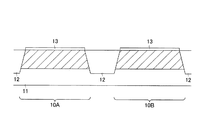
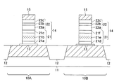
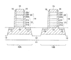
図1は、本発明の好ましい実施形態に係る半導体装置100の構造を示す略断面図である。
FIG. 1 is a schematic cross-sectional view showing the structure of a
図1に示すように、この半導体装置100はデュアルゲート構造のCMOSであって、n+ポリシリコンゲートを有するNMOSFET10Aと、p+ポリシリコンゲートを有するPMOSFET10Bとが同一基板上に形成されたものである。NMOSFET10A及びPMOSFET10Bは共に、シリコン基板11上に形成されたゲート絶縁膜13と、ゲート絶縁膜13上に形成されたゲート電極14と、ゲート電極14の上面を覆うゲートキャップ絶縁膜15と、ゲート電極14の側面を覆うサイドウォール絶縁膜16と、NMOSFET10Aのソース/ドレイン領域となる第1の拡散層17と、PMOSFET10Bのソース/ドレイン領域となる及び第2の拡散層18とを備えている。
As shown in FIG. 1, this
ゲート電極14はポリメタルゲート構造を有しており、3層構造のポリシリコン多層膜21と、ポリシリコン多層膜21上に形成された金属シリサイド多層膜22とを備えている。金属シリサイド多層膜22の構造はNMOSFET及びPMOSFET共に共通であり、タングステンシリサイド(WSi)膜22a、窒化タングステン(WN)膜22b、及びタングステン(W)膜22cがこの順に積層された構造を有している。これに対し、ポリシリコン多層膜21の構造はNMOSFET10AとPMOSFET10Bとで異なる。
The
NMOSFET10Aのポリシリコン多層膜21は、リン(P)等のn型不純物がドープされた第1乃至第3のドープドポリシリコン膜21a、21b、21cがこの順に積層された3層構造を有している。第1及び第3のドープドポリシリコン膜21a、21c中のn型不純物の濃度は、第2のドープドポリシリコン膜中のn型不純物の濃度よりも低い。この3層構造は、PMOSFET10Bのポリシリコン多層膜21を3層構造にすることに伴って形成されたものであり、NMOSFET10Aにおいて3層構造自体が特別な意味を持つものではない。このように、ポリシリコン多層膜21の各層にn型不純物がドープされていることから、ポリシリコン多層膜21はn+ポリシリコンゲートとして機能する。
The
一方、PMOSFET10Bのポリシリコン膜21は、リン(P+)等のn型不純物がドープされた第1のドープドポリシリコン膜21d、ホウ素(B+)等のp型不純物がドープされた第2のドープドポリシリコン膜21e、及び第1のドープドポリシリコン膜21dと同じくn型不純物がドープされた第3のドープドポリシリコン膜21fがこの順に積層された3層構造を有している。
On the other hand, the
PMOSFET10Bにおいて、第1及び第3のドープドポリシリコン膜21d、21fは、第2のドープドポリシリコン膜21e中のp型不純物の過度な拡散を阻止する役割を果たす。PMOSFET10Bのゲート電極14をp+ポリシリコンゲートとして構成するためには、p型不純物の濃度がn型不純物よりも十分に高くなければならない。そのため、第1及び第3のドープドポリシリコン膜21d、21f中のn型不純物の濃度は、その役割を果たすことができる限りにおいて十分低い濃度に設定されている。これに対して、第2のドープドポリシリコン膜21eの膜中には、ポリシリコン多層膜21を実際にp+ゲートとして機能させるに十分な高濃度のp型不純物が分布している。
In the
PMOSFET10Bのポリシリコン多層膜21は、バイポーラトランジスタのようにNPN接合となってはならない。NPN接合構造では抵抗が大きくなり、ゲートの性能が低下するからである。そのためには、後の製造工程(例えばDRAM製造工程)で一般的に存在する各種の高温熱負荷工程にてn型不純物とp型不純物が混ざり合い、ポリシリコン多層膜21中の全体でn型不純物よりもp型不純物の濃度が濃くなるようにし、これをp+ポリシリコンゲートとすればよい。単に混ぜ合わせるだけならば簡単であるが、不純物の外部放出などが顕著に起こるため、本発明のようなサンドイッチ構造を採用することによって不純物拡散を制御するわけである。
The
次に、半導体装置100の製造方法について詳細に説明する。
Next, a method for manufacturing the
図2〜図11は、本発明の好ましい実施形態による半導体装置100の製造工程を示す略断面図である。
2 to 11 are schematic cross-sectional views showing manufacturing steps of the
半導体装置100の製造では、まず図2に示すように、シリコン基板11上にフィールド酸化膜からなる素子分離領域12をSTI法により形成し、素子分離領域12によって互いに分離された活性領域を形成する。次に、一方の活性領域内にPウェル形成のためのイオン注入、トランジスタのパンチスルー阻止を目的とした埋め込み層形成のためのイオン注入、及び閾値電圧Vth調整のためのイオン注入を行って、NMOSチャネル領域10Aを形成する。また、他方の活性領域内にNウェル形成のためのイオン注入、トランジスタのパンチスルー阻止を目的とした埋め込み層形成のためのイオン注入、及び閾値電圧Vth調整のためのイオン注入を行って、PMOSチャネル領域10Bを形成する。
In manufacturing the
次に、図3に示すように、NMOSチャネル領域10A及びPMOSチャネル領域10Bの両方にゲート絶縁膜13を形成する。ゲート絶縁膜13の形成では、まず5nm程度の膜厚を有するシリコン酸化膜(SiO2)を熱酸化により形成する。その後、900℃程度の酸化雰囲気中で60秒程度の熱処理を行い、シリコン酸化膜を窒化することにより、シリコン窒化酸化膜(SiON)からなるゲート絶縁膜13が完成する。
Next, as shown in FIG. 3, the
次に、ゲート絶縁膜13上にアモルファスシリコン多層膜31を形成する。アモルファスシリコン多層膜31は以下に示すステップにより形成される。
Next, an amorphous
まず、図4に示すように、ゲート絶縁膜13上にリン(P)等のn型不純物がドープされた第1のドープドアモルファスシリコン膜31aを形成する。この膜は、シランガス(SiH4)を原料ガスとするLPCVD(Low-Pressured Chemical Vapor Deposition)法により形成することができ、特に、リンドープ用原料ガスを導入しながらドープドアモルファスシリコン膜を堆積する、いわゆる"In-Situ"により形成しても良い。第1のドープドアモルファスシリコン膜31aは10〜50nm程度の膜厚を有することが好ましい。
First, as shown in FIG. 4, a first doped
次に、図5に示すように、第1のドープドアモルファスシリコン膜31a上にノンドープドアモルファスシリコン膜31bを形成する。この膜も、シランガス(SiH4)を原料ガスとするLPCVD法により形成することができ、リンドープ用原料ガスの導入を中断することで、第1のドープドアモルファスシリコン膜31aからノンドープドアモルファスシリコン膜31bへの成膜工程を同一チャンバー内で連続的に行うことができる。ノンドープドアモルファスシリコン膜31bは10〜200nm程度の膜厚を有することが好ましい。
Next, as shown in FIG. 5, a non-doped
次に、図6に示すように、ノンドープドアモルファスシリコン膜31b上にリン(P)等のn型不純物がドープされた第2のドープドアモルファスシリコン膜31cを形成する。この膜も、シランガス(SiH4)を原料ガスとするLPCVD法により形成することができ、リンドープ用原料ガスの導入を再開することで、ノンドープドアモルファスシリコン膜31bから第2のドープドアモルファスシリコン膜31cへの成膜工程を同一チャンバー内で連続的に行うことができる。第2のドープドアモルファスシリコン膜31cは10〜50nm程度の膜厚を有することが好ましい。
Next, as shown in FIG. 6, a second doped
次に、NMOSチャネル領域10A内のノンドープドアモルファスシリコン膜31b及びPMOSチャネル領域10B内のノンドープドアモルファスシリコン膜31b中にリン(P+)及びホウ素(B+)をそれぞれイオン注入する。この工程は2回のイオン注入工程に分けて行われる。
Next, phosphorus (P + ) and boron (B + ) are ion-implanted into the non-doped
まず、図7に示すように、PMOSチャネル領域10Bをマスクしながら、NMOSチャネル領域10A内のノンドープドアモルファスシリコン膜31b中にリン(P+)をイオン注入する。このときの注入エネルギーは5〜30keV程度、ドーズ量は、1×1014cm−2〜5×1015cm−2であることが好ましい。こうしてノンドープドアモルファスシリコン膜31b中に高濃度のリン(P+)が導入されることにより、アモルファスシリコン全体はn+シリコンゲートとなる。
First, as shown in FIG. 7, phosphorus (P + ) ions are implanted into the non-doped
次いで、図8に示すように、NMOSチャネル領域10Aをマスクしながら、PMOSチャネル領域10B内のノンドープドアモルファスシリコン膜31b中にホウ素(B+)をイオン注入する。このときの注入エネルギーは1〜20keV程度、ドーズ量は、1×1014cm−2〜1×1016cm−2であることが好ましい。このように、リン(P)が含まれているアモルファスシリコン膜中にホウ素(B+)を打ち返すことにより、アモルファスシリコン膜中のホウ素の濃度が高くなるので、アモルファスシリコン全体はp+ゲートとなる。
Next, as shown in FIG. 8, boron (B + ) is ion-implanted into the non-doped
なお、イオン注入工程の順番は特に限定されず、PMOSチャネル領域10B及びNMOSチャネル領域10Aのどちらを先に行ってもかまわない。
The order of the ion implantation steps is not particularly limited, and either the
次に、図9に示すように、アモルファスシリコン多層膜31上に金属シリサイド多層膜22を形成する。本実施形態においては、金属シリサイド多層膜22としてタングステンシリサイド(WSi)膜22a、窒化タングステン膜(WN)22b、及びタングステン膜(W)22cをこの順に形成する。タングステンシリサイド膜22aは、例えば六フッ化タングステン(WF6)ガスとジクロロシラン(SiCl2H2)ガスを原料ガスとし、かつ580℃の温度条件下でLPCVD法により形成することができる。タングステンシリサイド膜22aは1〜20nm程度の膜厚を有することが好ましい。また、窒化タングステン膜22bはスパッタリングにより形成することができ、10〜20nmの膜厚を有することが好ましい。また、タングステン膜22cはスパッタリングにより形成することができ、50〜100nmの膜厚を有することが好ましい。
Next, as shown in FIG. 9, a metal
次に、図10に示すように、金属シリサイド多層膜22上に30nm程度の膜厚を有するシリコン酸化膜を形成した後、フォトリソグラフィ及びエッチングを用いて、ポリシリコン多層膜21、金属シリサイド多層膜22、及びシリコン酸化膜をパターニングし、ゲート電極14及びゲートキャップ絶縁膜15を形成する。さらに、図11に示すように、基板全面に30nm程度の膜厚を有するシリコン酸化膜を形成した後、これをエッチバックすることにより、ゲート電極14の側面にサイドウォール絶縁膜16を形成する。
Next, as shown in FIG. 10, after a silicon oxide film having a film thickness of about 30 nm is formed on the metal
その後、NMOSFET側のソース/ドレイン領域である第1の拡散層17、PMOSFET側のソース/ドレイン領域である第2の拡散層18を周知の方法で順次形成する。以上の工程により、デュアルゲート構造のCMOSトランジスタを備えた半導体装置100が完成する。
Thereafter, a
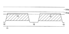
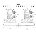
さらに、図12に示すように、半導体装置100が後の製造工程(例えばDRAM製造工程)で一般的に存在する各種の高温熱負荷工程を経ることにより、アモルファスシリコン多層膜21中のリン(P+)及びホウ素(B+)は拡散するが、異種の不純物が同時に存在する場合、それぞれの不純物が互いの拡散を抑制し合うので、注入されたドーパント(ホウ素)は、ノンドープドアモルファスシリコン膜内では拡散しやすく、リン(P+)ドープドアモルファスシリコン膜内では拡散しにくい。つまり、図6に示したように、ノンドープドアモルファスシリコン膜31bの上下は第1及び第2のリンドープドアモルファスシリコン膜に挟まれているので、PMOSFET側においてホウ素(B+)の過度な拡散が抑制される。したがって、ホウ素(B)がゲート絶縁膜13を突き抜ける現象を抑制することができ、またタングステンシリサイド膜によるポリシリコン膜中のホウ素(B+)の吸収を抑制することができる。なお、熱負荷によってアモルファスシリコンの結晶化が進み、アモルファスシリコンはポリシリコンに変化する。
Furthermore, as shown in FIG. 12, the
以上説明したように、本実施形態に係る半導体装置100の製造方法によれば、ゲート絶縁膜13上の第1乃至第3アモルファスシリコン膜を形成すると共に、第1及び第3のアモルファスシリコン膜中の不純物の導電型を、それらの間に挟まれる第2のアモルファスシリコン膜中に導入される不純物と異ならせ、異種の不純物が互いの拡散を抑制し合う現象を利用して、第2層目の不純物が外部へ流出することを抑制することができる。
As described above, according to the method for manufacturing the
以上、本発明をその好ましい実施形態に基づき説明したが、本発明は上記実施形態に限定されることなく、本発明の趣旨を逸脱しない範囲内で種々の変更を加えることが可能であり、それらも本発明の範囲に包含されるものであることは言うまでもない。 Although the present invention has been described based on the preferred embodiments, the present invention is not limited to the above-described embodiments, and various modifications can be made without departing from the spirit of the present invention. Needless to say, these are also included in the scope of the present invention.
例えば、上記実施形態においては、NMOSFETの第1及び第3のアモルファスシリコン膜にリン(P)等のn型不純物を導入しているが、本発明はこのような構成に限定されるものではなく、第1層目及び第3層目にホウ素(B)等のp型不純物が導入されたドープドアモルファスシリコン膜を用い、2層目のノンドープドアモルファスシリコン膜31bにリン(P+)等のn型不純物をイオン注入してもよい。リン等のn型不純物は、ホウ素(B)等のp型不純物ほど拡散しやすいものではないが、第1層目と第3層目にn型不純物を導入することで、2層目に導入されたp型不純物の過度な拡散を防止することができる。
For example, in the above embodiment, n-type impurities such as phosphorus (P) are introduced into the first and third amorphous silicon films of the NMOSFET, but the present invention is not limited to such a configuration. A doped amorphous silicon film into which p-type impurities such as boron (B) are introduced in the first layer and the third layer is used, and phosphorus (P + ) or the like is formed on the second non-doped
また、上記実施形態においては、ポリメタルゲートを採用し、タングステンシリサイド、窒化タングステン、及びタングステンからなる3層構造の金属シリサイド多層膜22を用いているが、本発明においてポリメタルゲート構造を採用することは必須でない。また、メタルを省略し、タングステンシリサイドの単層膜で構成されていても構わない。
In the above embodiment, a polymetal gate is used and the metal
また、上記実施形態においては、アモルファスシリコン膜を3層構造としているが、2層構造とすることも可能である。すなわち、第2のアモルファスシリコン膜の上層に金属シリサイド膜を形成しない場合には、シリサイド層による不純物吸収の問題が生じないことから、ゲート絶縁膜13とノンドープドアモルファスシリコン膜31bとの間にのみバリア層としてのドープドアモルファスシリコン膜を形成すればよい。
In the above-described embodiment, the amorphous silicon film has a three-layer structure, but a two-layer structure may be used. That is, when the metal silicide film is not formed on the second amorphous silicon film, the problem of impurity absorption by the silicide layer does not occur, and therefore only between the
また、上記実施形態においては、NMOSチャネル領域10A内のノンドープドアモルファスシリコン膜31b中にリン(P+)をイオン注入する第1のイオン注入工程と、PMOSチャネル領域10B内のノンドープドアモルファスシリコン膜31b中にホウ素(B+)をイオン注入する第2のイオン注入工程の各々でマスクを使用し、ホウ素(B+)とリン(P+)の打ち分けを行っているが、本発明はこのようなイオン注入工程に限定されるものではなく、例えば、NMOSチャネル領域10AとPMOSチャネル領域10Bの両方にリンをイオン注入した後、NMOSチャネル領域10Aのみをマスクして、PMOSチャネル領域10Bリンよりも高濃度のホウ素を打ち返してもよい。このイオン注入工程によれば、1回のマスク処理にてホウ素とリンをそれぞれ所定の領域に導入することができる。また、注入深さで調整しても良い。
In the above embodiment, the first ion implantation step of ion-implanting phosphorus (P + ) into the non-doped
10A NMOSチャネル領域
10B PMOSチャネル領域
11 シリコン基板
13 ゲート絶縁膜
14 ゲート電極
14 ドープドポリシリコン膜
15 ゲートキャップ絶縁膜
16 サイドウォール絶縁膜
17 第1の拡散層
18 第2の拡散層
21 ポリシリコン多層膜
21a 第1のドープドポリシリコン膜
21b 第2のドープドポリシリコン膜
21c 第3のドープドポリシリコン膜
21d 第1のドープドポリシリコン膜
21e 第2のドープドポリシリコン膜
21f 第3のドープドポリシリコン膜
22 金属シリサイド多層膜
22a タングステンシリサイド膜
22b 窒化タングステン膜
22c タングステン膜
31 アモルファスシリコン多層膜
31a 第1のドープドアモルファスシリコン膜
31b ノンドープドアモルファスシリコン膜
31c 第2のドープドアモルファスシリコン膜
51 シリコン基板
52 ゲート絶縁膜
53 ノンドープドアモルファスシリコン膜
54 金属シリサイド膜
100 半導体装置
10A
Claims (16)
前記シリコン基板上に形成されたゲート絶縁膜と、
前記ゲート絶縁膜上に形成されたゲート電極とを備え、
前記ゲート電極は、
前記ゲート絶縁膜上に形成された第1のドープドポリシリコン膜と、
前記第1のドープドポリシリコン膜上に形成された第2のドープドポリシリコン膜とを備え、
前記第1のドープドポリシリコン膜は、第1の不純物を含み、
前記第2のドープドポリシリコン膜は、前記第1の不純物とは反対の導電型を有する第2の不純物を含むことを特徴とする半導体装置。 A silicon substrate;
A gate insulating film formed on the silicon substrate;
A gate electrode formed on the gate insulating film,
The gate electrode is
A first doped polysilicon film formed on the gate insulating film;
A second doped polysilicon film formed on the first doped polysilicon film;
The first doped polysilicon film includes a first impurity;
The semiconductor device according to claim 2, wherein the second doped polysilicon film includes a second impurity having a conductivity type opposite to that of the first impurity.
前記第2のドープドポリシリコン膜上に形成された第3のドープドポリシリコン膜をさらに備え、
前記第3のドープドポリシリコン膜は、前記第1の不純物を含むことを特徴とする請求項1に記載の半導体装置。 The gate electrode is
A third doped polysilicon film formed on the second doped polysilicon film;
The semiconductor device according to claim 1, wherein the third doped polysilicon film contains the first impurity.
前記第3のドープドポリシリコン膜上に形成された金属シリサイド膜をさらに備えることを特徴とする請求項2に記載の半導体装置。 The gate electrode is
The semiconductor device according to claim 2, further comprising a metal silicide film formed on the third doped polysilicon film.
前記ゲート絶縁膜上にゲート電極を形成するゲート電極形成工程と、
前記シリコン基板全体に熱負荷を加える熱負荷工程とを備え、
前記ゲート電極形成工程は、
前記ゲート絶縁膜上に第1の不純物がドープされた第1のドープドアモルファスシリコン膜を形成する第1のドープドアモルファスシリコン膜形成工程と、
前記第1のドープドアモルファスシリコン膜上にノンドープドアモルファスシリコン膜を形成するノンドープドアモルファスシリコン膜形成工程と、
前記ノンドープドアモルファスシリコン膜中に前記第1の不純物とは逆の導電型を有する第2の不純物をイオン注入するイオン注入工程とを備えることを特徴とする半導体装置の製造方法。 A gate insulating film forming step of forming a gate insulating film on the silicon substrate;
Forming a gate electrode on the gate insulating film; and
A heat load step of applying a heat load to the entire silicon substrate,
The gate electrode forming step includes
A first doped amorphous silicon film forming step of forming a first doped amorphous silicon film doped with a first impurity on the gate insulating film;
A non-doped amorphous silicon film forming step of forming a non-doped amorphous silicon film on the first doped amorphous silicon film;
A method of manufacturing a semiconductor device, comprising: an ion implantation step of ion-implanting a second impurity having a conductivity type opposite to that of the first impurity into the non-doped amorphous silicon film.
前記ノンドープドアモルファスシリコン膜上に前記第1の不純物がドープされた第2のドープドアモルファスシリコン膜を形成する第2のドープドアモルファスシリコン膜形成工程をさらに備えることを特徴とする請求項7に記載の半導体装置の製造方法。 The gate electrode forming step includes
8. The method according to claim 7, further comprising a second doped amorphous silicon film forming step of forming a second doped amorphous silicon film doped with the first impurity on the non-doped amorphous silicon film. The manufacturing method of the semiconductor device of description.
前記イオン注入工程の後、前記第2のドープドアモルファスシリコン膜上に金属シリサイド膜を形成する金属シリサイド膜形成工程をさらに備えることを特徴とする請求項8に記載の半導体装置の製造方法。 The gate electrode forming step includes
9. The method of manufacturing a semiconductor device according to claim 8, further comprising a metal silicide film forming step of forming a metal silicide film on the second doped amorphous silicon film after the ion implantation step.
前記ゲート絶縁膜上にゲート電極を形成するゲート電極形成工程と、
前記シリコン基板全体に熱負荷を加える熱負荷工程とを備え、
前記ゲート電極形成工程は、
前記ゲート絶縁膜上にn型不純物がドープされた第1のドープドアモルファスシリコン膜を形成する第1のドープドアモルファスシリコン膜形成工程と、
前記第1のドープドアモルファスシリコン膜上にノンドープドアモルファスシリコン膜を形成するノンドープドアモルファスシリコン膜形成工程と、
前記PMOSチャネル領域内の前記ノンドープドアモルファスシリコン膜中にp型不純物をイオン注入すると共に、前記NMOSチャネル領域内の前記ノンドープドアモルファスシリコン膜中にn型不純物をイオン注入するイオン注入工程とを備えることを特徴とする半導体装置の製造方法。 Forming a gate insulating film in the NMOS channel region and the PMOS channel region on the silicon substrate; and
Forming a gate electrode on the gate insulating film; and
A heat load step of applying a heat load to the entire silicon substrate,
The gate electrode forming step includes
Forming a first doped amorphous silicon film doped with an n-type impurity on the gate insulating film;
A non-doped amorphous silicon film forming step of forming a non-doped amorphous silicon film on the first doped amorphous silicon film;
An ion implantation step of ion-implanting p-type impurities into the non-doped amorphous silicon film in the PMOS channel region and ion-implanting n-type impurities into the non-doped amorphous silicon film in the NMOS channel region. A method for manufacturing a semiconductor device.
Priority Applications (2)
| Application Number | Priority Date | Filing Date | Title |
|---|---|---|---|
| JP2007234173A JP2009070840A (en) | 2007-09-10 | 2007-09-10 | Semiconductor device and manufacturing method thereof |
| US12/207,152 US20090065779A1 (en) | 2007-09-10 | 2008-09-09 | Semiconductor device and manufacturing method thereof |
Applications Claiming Priority (1)
| Application Number | Priority Date | Filing Date | Title |
|---|---|---|---|
| JP2007234173A JP2009070840A (en) | 2007-09-10 | 2007-09-10 | Semiconductor device and manufacturing method thereof |
Publications (1)
| Publication Number | Publication Date |
|---|---|
| JP2009070840A true JP2009070840A (en) | 2009-04-02 |
Family
ID=40430864
Family Applications (1)
| Application Number | Title | Priority Date | Filing Date |
|---|---|---|---|
| JP2007234173A Abandoned JP2009070840A (en) | 2007-09-10 | 2007-09-10 | Semiconductor device and manufacturing method thereof |
Country Status (2)
| Country | Link |
|---|---|
| US (1) | US20090065779A1 (en) |
| JP (1) | JP2009070840A (en) |
Cited By (1)
| Publication number | Priority date | Publication date | Assignee | Title |
|---|---|---|---|---|
| KR20110100504A (en) * | 2010-03-04 | 2011-09-14 | 삼성전자주식회사 | Semiconductor device and method of fabricating the same |
Families Citing this family (8)
| Publication number | Priority date | Publication date | Assignee | Title |
|---|---|---|---|---|
| KR101026386B1 (en) * | 2009-05-06 | 2011-04-07 | 주식회사 하이닉스반도체 | Method for fabricating dual poly gate in semiconductor device |
| KR101683072B1 (en) * | 2010-09-13 | 2016-12-21 | 삼성전자 주식회사 | Method Of Forming Semiconductor Device |
| JP2012151435A (en) * | 2010-12-27 | 2012-08-09 | Elpida Memory Inc | Method for manufacturing semiconductor device |
| US20120276730A1 (en) * | 2011-04-27 | 2012-11-01 | Nanya Technology Corporation | Methods for fabricating a gate dielectric layer and for fabricating a gate structure |
| TWI550830B (en) * | 2014-05-23 | 2016-09-21 | 旺宏電子股份有限公司 | Semiconductor structure and method for manufacturing the same |
| CN105226061B (en) * | 2014-06-10 | 2018-04-24 | 旺宏电子股份有限公司 | Semiconductor structure and its manufacture method |
| US9252155B2 (en) * | 2014-06-20 | 2016-02-02 | Macronix International Co., Ltd. | Memory device and method for manufacturing the same |
| CN105280486B (en) * | 2014-07-23 | 2020-09-22 | 联华电子股份有限公司 | Method for manufacturing metal gate structure |
Family Cites Families (9)
| Publication number | Priority date | Publication date | Assignee | Title |
|---|---|---|---|---|
| JPH0734477B2 (en) * | 1990-05-28 | 1995-04-12 | 株式会社東芝 | Method for manufacturing semiconductor device |
| US6265259B1 (en) * | 1998-02-06 | 2001-07-24 | Texas Instruments-Acer Incorporated | Method to fabricate deep sub-μm CMOSFETs |
| US6162711A (en) * | 1999-01-15 | 2000-12-19 | Lucent Technologies, Inc. | In-situ boron doped polysilicon with dual layer and dual grain structure for use in integrated circuits manufacturing |
| US6137145A (en) * | 1999-01-26 | 2000-10-24 | Advanced Micro Devices, Inc. | Semiconductor topography including integrated circuit gate conductors incorporating dual layers of polysilicon |
| KR100353551B1 (en) * | 2000-01-28 | 2002-09-27 | 주식회사 하이닉스반도체 | Method of forming silicide |
| US20030092249A1 (en) * | 2001-11-09 | 2003-05-15 | Chia-Fu Hsu | Lightly-insitu-doped amorphous silicon applied in DRAM gates |
| US7164161B2 (en) * | 2003-11-18 | 2007-01-16 | Micron Technology, Inc. | Method of formation of dual gate structure for imagers |
| JP4782411B2 (en) * | 2004-12-16 | 2011-09-28 | エルピーダメモリ株式会社 | Semiconductor device and manufacturing method thereof |
| KR100753546B1 (en) * | 2006-08-22 | 2007-08-30 | 삼성전자주식회사 | Gate of transistor and method for forming the same |
-
2007
- 2007-09-10 JP JP2007234173A patent/JP2009070840A/en not_active Abandoned
-
2008
- 2008-09-09 US US12/207,152 patent/US20090065779A1/en not_active Abandoned
Cited By (5)
| Publication number | Priority date | Publication date | Assignee | Title |
|---|---|---|---|---|
| KR20110100504A (en) * | 2010-03-04 | 2011-09-14 | 삼성전자주식회사 | Semiconductor device and method of fabricating the same |
| US8476692B2 (en) | 2010-03-04 | 2013-07-02 | Samsung Electronics Co., Ltd. | Semiconductor devices and methods of manufacturing the same |
| US9129950B2 (en) | 2010-03-04 | 2015-09-08 | Samsung Electronics Co., Ltd. | Semiconductor devices |
| US9443863B2 (en) | 2010-03-04 | 2016-09-13 | Samsung Electronics Co., Ltd. | Semiconductor devices |
| KR101688614B1 (en) | 2010-03-04 | 2016-12-22 | 삼성전자주식회사 | Transistor |
Also Published As
| Publication number | Publication date |
|---|---|
| US20090065779A1 (en) | 2009-03-12 |
Similar Documents
| Publication | Publication Date | Title |
|---|---|---|
| KR100487525B1 (en) | Semiconductor device using silicon-germanium gate and method for fabricating the same | |
| US7132322B1 (en) | Method for forming a SiGe or SiGeC gate selectively in a complementary MIS/MOS FET device | |
| US6642132B2 (en) | Cmos of semiconductor device and method for manufacturing the same | |
| JP4271920B2 (en) | Semiconductor device CMOS and method of manufacturing the same | |
| JP2009070840A (en) | Semiconductor device and manufacturing method thereof | |
| KR100591344B1 (en) | Manufacturing method of semiconductor device | |
| US7947547B2 (en) | Method for manufacturing a semiconductor device | |
| JP2005136351A (en) | Semiconductor device and manufacturing method therefor | |
| JP2008103644A (en) | Semiconductor device and production method thereof | |
| JP2006202860A (en) | Semiconductor device and its manufacturing method | |
| US20050236667A1 (en) | Manufacture of semiconductor device with selective amorphousizing | |
| JP4767843B2 (en) | Semiconductor device and manufacturing method thereof | |
| JP2005340329A (en) | Semiconductor device and its manufacturing method | |
| JP3339361B2 (en) | Semiconductor device | |
| JP4828982B2 (en) | Manufacturing method of semiconductor device | |
| JP5324849B2 (en) | Semiconductor device and manufacturing method thereof | |
| JP2007288051A (en) | Semiconductor device, and manufacturing method thereof | |
| US7271414B2 (en) | Semiconductor device and method for fabricating the same | |
| KR100691491B1 (en) | Dual gate of semiconductor device and method for forming the same | |
| JP4115769B2 (en) | Semiconductor device and manufacturing method thereof | |
| JP2009123991A (en) | Method of manufacturing semiconductor device, and semiconductor device | |
| JP2008258354A (en) | Semiconductor device, and manufacturing method thereof | |
| US20070200151A1 (en) | Semiconductor device and method of fabricating the same | |
| US20100019327A1 (en) | Semiconductor Device and Method of Fabricating the Same | |
| JPH1056171A (en) | Mis semiconductor device and its manufacture |
Legal Events
| Date | Code | Title | Description |
|---|---|---|---|
| A621 | Written request for application examination |
Free format text: JAPANESE INTERMEDIATE CODE: A621 Effective date: 20100805 |
|
| A762 | Written abandonment of application |
Free format text: JAPANESE INTERMEDIATE CODE: A762 Effective date: 20101130 |