JP2009063577A - Analytical test strip with improved reagent deposition - Google Patents
Analytical test strip with improved reagent deposition Download PDFInfo
- Publication number
- JP2009063577A JP2009063577A JP2008225762A JP2008225762A JP2009063577A JP 2009063577 A JP2009063577 A JP 2009063577A JP 2008225762 A JP2008225762 A JP 2008225762A JP 2008225762 A JP2008225762 A JP 2008225762A JP 2009063577 A JP2009063577 A JP 2009063577A
- Authority
- JP
- Japan
- Prior art keywords
- electrode
- microns
- conductive material
- layer
- working electrode
- Prior art date
- Legal status (The legal status is an assumption and is not a legal conclusion. Google has not performed a legal analysis and makes no representation as to the accuracy of the status listed.)
- Pending
Links
Images


Classifications
-
- C—CHEMISTRY; METALLURGY
- C12—BIOCHEMISTRY; BEER; SPIRITS; WINE; VINEGAR; MICROBIOLOGY; ENZYMOLOGY; MUTATION OR GENETIC ENGINEERING
- C12Q—MEASURING OR TESTING PROCESSES INVOLVING ENZYMES, NUCLEIC ACIDS OR MICROORGANISMS; COMPOSITIONS OR TEST PAPERS THEREFOR; PROCESSES OF PREPARING SUCH COMPOSITIONS; CONDITION-RESPONSIVE CONTROL IN MICROBIOLOGICAL OR ENZYMOLOGICAL PROCESSES
- C12Q1/00—Measuring or testing processes involving enzymes, nucleic acids or microorganisms; Compositions therefor; Processes of preparing such compositions
- C12Q1/001—Enzyme electrodes
-
- G—PHYSICS
- G01—MEASURING; TESTING
- G01N—INVESTIGATING OR ANALYSING MATERIALS BY DETERMINING THEIR CHEMICAL OR PHYSICAL PROPERTIES
- G01N27/00—Investigating or analysing materials by the use of electric, electrochemical, or magnetic means
- G01N27/26—Investigating or analysing materials by the use of electric, electrochemical, or magnetic means by investigating electrochemical variables; by using electrolysis or electrophoresis
- G01N27/28—Electrolytic cell components
- G01N27/30—Electrodes, e.g. test electrodes; Half-cells
- G01N27/327—Biochemical electrodes, e.g. electrical or mechanical details for in vitro measurements
- G01N27/3271—Amperometric enzyme electrodes for analytes in body fluids, e.g. glucose in blood
- G01N27/3272—Test elements therefor, i.e. disposable laminated substrates with electrodes, reagent and channels
-
- G—PHYSICS
- G01—MEASURING; TESTING
- G01N—INVESTIGATING OR ANALYSING MATERIALS BY DETERMINING THEIR CHEMICAL OR PHYSICAL PROPERTIES
- G01N33/00—Investigating or analysing materials by specific methods not covered by groups G01N1/00 - G01N31/00
- G01N33/48—Biological material, e.g. blood, urine; Haemocytometers
- G01N33/50—Chemical analysis of biological material, e.g. blood, urine; Testing involving biospecific ligand binding methods; Immunological testing
- G01N33/52—Use of compounds or compositions for colorimetric, spectrophotometric or fluorometric investigation, e.g. use of reagent paper and including single- and multilayer analytical elements
- G01N33/521—Single-layer analytical elements
Abstract
Description
本発明は、試薬の被着を改善した分析用の試験片に関する。 The present invention relates to an analytical test strip with improved reagent deposition.
流体サンプル中の分析物濃度を決定するための電気化学的方法および装置は、糖尿病などの医療疾患の治療および管理において広く適用される。糖尿病を患う患者はそのような方法を用いて、毎日数回、血液中のグルコース濃度をモニターする場合が多い。 Electrochemical methods and devices for determining analyte concentration in a fluid sample are widely applied in the treatment and management of medical diseases such as diabetes. Patients with diabetes often use such methods to monitor blood glucose levels several times daily.
電気化学的方法は、一般に電流、電位または蓄積電荷間の相関関係、および分析物の試薬濃度に依存し、概して、分析物と混合したときに荷電キャリアを生成する試薬と関連している。検査を行うための電気化学的バイオセンサーは一般に、使い捨て試験片であり、上部に試薬が設けられ、血液などの生物学的液体と化学的に反応する。試験片は試験測定器と対にして用いられ、試験測定器が分析物と試薬間の反応量を計測し、分析物の濃度を決定するようになっている。電気化学に基づく試験片では、試験片に付いている電気接着パッドを介して電気シグナルを測定器に伝送して、測定器の試験片ポートコネクタ内に接触する。 Electrochemical methods generally depend on the correlation between current, potential or accumulated charge, and the reagent concentration of the analyte, and are generally associated with reagents that produce charge carriers when mixed with the analyte. Electrochemical biosensors for performing tests are generally disposable test strips, which are provided with reagents on the top and chemically react with biological fluids such as blood. The test piece is used as a pair with a test measuring instrument, and the test measuring instrument measures the amount of reaction between the analyte and the reagent to determine the concentration of the analyte. In electrochemical-based test strips, an electrical signal is transmitted to the meter through an electrical bond pad attached to the test strip and contacts the test strip port connector of the meter.
既知の試験片製造技法では、金属被覆ポリマーフィルムの使用とフィルム上の導電性電極パターンの形成に関与する。レーザー剥離または化学的エッチングを含めた適切なエッチング処理を行いフィルムから導電性材料を除去すると電極パターンが所定位置に形成され、露出した基板材料と織り交ざった導電性のある電極パターンが残される。従って、電極パターンは、導電性材料間の露出したフィルムまたは基板材料の隙間によって画定される。 Known specimen manufacturing techniques involve the use of metal-coated polymer films and the formation of conductive electrode patterns on the films. When the conductive material is removed from the film by performing an appropriate etching process including laser peeling or chemical etching, an electrode pattern is formed at a predetermined position, and a conductive electrode pattern interwoven with the exposed substrate material is left. Thus, the electrode pattern is defined by exposed film or substrate material gaps between the conductive materials.
本出願人はレーザー剥離処理を施して作製されたプロトタイプ試験片の中には、試薬が電極パターン上に均一に被着されていないものがあることを発見した。本出願人はまた、このようなプロトタイプ試験片において、毛管効果によって継続して試薬と電極の検知領域に分析物サンプルを満たす性能が劣っていることを発見した。本出願人はこれらの問題が試験片の性能を落とす原因になると考える。 The Applicant has discovered that some prototype test specimens produced by laser stripping are not uniformly deposited on the electrode pattern. Applicants have also found that such prototype test strips have poor performance in filling analyte samples in the reagent and electrode sensing areas due to capillary effects. The applicant believes that these problems cause the specimen performance to degrade.
本出願人は様々な技術的機能を実装し、従来技術で利用不可能な本発明の様々な実施形態を提供することによってこの問題の解決を得た。一態様において、分析用の試験片は、基板、導電性材料、導電性材料の隔離部分を含む。基板は、一般に、表面が平らであり、第1の端部から第2の端部まで拡張している。略平坦な表面に導電性材料が設けられ、相互に離れた複数の電極が定義される。導電性材料の隔離部分は、少なくとも2個の電極間に設けられ、隔離部分は複数の電極と電気通信が行われない。 Applicants have solved this problem by implementing various technical functions and providing various embodiments of the present invention that are not available in the prior art. In one embodiment, the test specimen for analysis includes a substrate, a conductive material, and an isolated portion of the conductive material. The substrate generally has a flat surface and extends from the first end to the second end. A conductive material is provided on a substantially flat surface, and a plurality of electrodes separated from each other are defined. The isolation portion of the conductive material is provided between at least two electrodes, and the isolation portion is not in electrical communication with the plurality of electrodes.
別の態様では、液体サンプル中の分析物の濃度を測定するための分析物測定システムが提供される。このシステムは、測定器および試験片を含む。計測器は基準電極と作用電極間に試験電圧を印加するための電気回路とシグナルプロセッサを含む。試験は、試験片に液体サンプルを満たす間、毛管現象が支援されるように導電性材料の隔離部分によって分離される基準電極と作用電極を有する基板を含む。 In another aspect, an analyte measurement system for measuring the concentration of an analyte in a liquid sample is provided. The system includes a meter and a test strip. The instrument includes an electrical circuit and a signal processor for applying a test voltage between the reference electrode and the working electrode. The test includes a substrate having a reference electrode and a working electrode that are separated by an isolated portion of conductive material so that capillary action is supported while filling the test piece with a liquid sample.
さらなる態様において、液体サンプル中の分析物濃度を測定するための試験片が提供される。試験片は、基板材料を含む。基準電極は第1の作用電極が係る基準電極に隣接して基板上に設けられている。第2の作用電極は第1の作用電極に隣接して基板上に設けられている。導電性材料の隔離部分は、第1および第2の作用電極の何れかの近位に、また基準電極の遠位に配置される。 In a further aspect, a test strip is provided for measuring an analyte concentration in a liquid sample. The test piece includes a substrate material. The reference electrode is provided on the substrate adjacent to the first working electrode. The second working electrode is provided on the substrate adjacent to the first working electrode. An isolated portion of conductive material is disposed proximal to either of the first and second working electrodes and distal to the reference electrode.
さらに別の態様では、分析用の試験片の製造方法が提供される。この方法は基板に導電性材料の層を被着し、導電性材料の層から選択した部分を除去し、少なくとも1つの電気的に隔離された導電性材料からなるアイランドとともに複数の電極を定義することによって達成される。このアイランドは、いずれの電極から約50ミクロン以下の距離を持たせ、電極からアイランドを電気的に隔離する。 In yet another aspect, a method for producing a test strip for analysis is provided. The method deposits a layer of conductive material on a substrate, removes selected portions from the layer of conductive material, and defines a plurality of electrodes with an island of at least one electrically isolated conductive material. Is achieved. The island has a distance of about 50 microns or less from either electrode to electrically isolate the island from the electrode.
上記または他の実施形態、特徴、利点は、当業者であれば以下に最初に簡単に説明される添付の図とともに以下に詳細に説明する本発明の方法およびシステムの細部を読むと明らかになろう。 These and other embodiments, features, and advantages will become apparent to those of ordinary skill in the art upon reading the details of the method and system of the present invention described in detail below in conjunction with the accompanying drawings, which are briefly described first below. Let's go.
本明細書に取り込まれ、その一部を構成する添付の図面は、本発明の好適な実施形態を詳細に説明し、上記の一般的な説明および下記の詳細な説明と共に、本発明の特徴を説明することに役立つ(同様の数値が同様の要素を示している) The accompanying drawings, which are incorporated in and constitute a part of this specification, illustrate preferred embodiments of the invention in detail, and together with the general description above and the detailed description below, characterize the invention. Help explain (similar numbers indicate similar elements)
以下の詳細な説明は図を参照しながら読むことに注意されたい。これらの図では異なる図の同様の要素が同一の符号で示される。図は必ずしも縮尺どおりではなく、選択した実施形態を図示し、本発明の範囲を限定するものではない。詳細な説明は例示的目的のものであって、限定するものではなく、本発明の原理を示す。この説明は、当業者が本発明を作成し、用いることを可能にするために提示され、現在認識される本発明の最良のモードの例示を含み複数の実施形態、適用例、バリエーション、改変、使用を記述する。 Note that the following detailed description is read with reference to the figures. In these figures, similar elements in different figures are denoted by the same reference numerals. The figures are not necessarily to scale, and illustrate selected embodiments and are not intended to limit the scope of the invention. The detailed description is for illustrative purposes and is not limiting and illustrates the principles of the invention. This description is presented to enable those skilled in the art to make and use the invention, and includes a number of embodiments, applications, variations, modifications, including illustrations of the best mode of the invention currently recognized. Describe use.
任意の数値または範囲用に使用される本明細書の用語である「約」(about)または「おおよそ」(approximately)は適切な寸法公差を示し、構成要素の部分または集合が本明細書に記載のとおり、意図する目的のために機能することを可能にする。加えて本明細書で使用される「患者」、「宿主」および「対象」の用語は任意のヒトまたは動物の対象を参照し、ヒトの患者における対象の発明の使用が好ましい実施形態を表す場合でもシステムまたは方法をヒトの使用に制限する意図を持たない。 As used herein, the terms “about” or “approximate” used for any numerical value or range indicate an appropriate dimensional tolerance, and a component part or set is described herein. As such, it can function for the intended purpose. In addition, as used herein, the terms “patient”, “host” and “subject” refer to any human or animal subject, where the use of the subject invention in a human patient represents a preferred embodiment. But it is not intended to limit the system or method to human use.
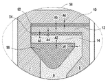
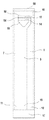
図1および図1Bは試験片90が第1の端部3および第2の端部4を有する例示的な実施形態を図示する。第1または遠位端部3は図1Bに示されるようにバイオセンシング部分を含む。第2または近位端部4は電気接触部分を含む。
1 and 1B illustrate an exemplary embodiment in which a
図1Bにおいて、バイオセンシングの部分がそれぞれ3つの電極10、12、および14とともに提供される。電極は一般に同一の導電性材料であり得る。電極10と12の間には、第1の電気的に隔離されたアイランド52が提供される。同様に第2の電気的に隔離されたアイランド54が電極12と14の間に提供される。同様に第3の電気的に隔離されたアイランド56が第3の電極14に対し遠位位置に、また近位部分4により近い位置で提供される。導電性のあるアイランド52、54および56はそれぞれ一般に1つまたは複数の電極と同一の導電性材料から製造し得る。さらに、各「アイランド」は、試験片90の電極10、12および14から電気的に隔離することが意図している。
In FIG. 1B, the biosensing portion is provided with three
図1Cに示されているように試験片90は基板上に複数の個別の構成要素を層にして製造し得る。特に、これらの層は導電層50、試薬層22、スペーサー層60および親水性の接着剤塗膜を施した上部層またはカバー80を含んでもよい。試験片90は導電層50および試薬層22が、例として米国特許出願公開番号US20050096409A1号および国際公開番号第WO2004040948A1号、同第WO2004040290A1、同第WO2004040287A1、同第WO2004040285A2、同第WO2004040005A1号、同第WO2004039897A2号、および同第WO2004039600A2号に説明されたスクリーン印刷プロセスを使用して基板5に順番に被着される一連の工程で製造される。別の実施形態では、インクジェット処理を使用して基板5に試薬層22が被着される。インクジェット処理は米国特許第6,179,979号に説明される。しかし、導電層50に試薬22を被着する別の処理には、ドロップオンデマンド処理が含まれる。スペーサー層60および上部層80はロールストックから取り出し、基板5にラミネート処理を施してもよい。別の実施形態において、スパッタリング処理を導電層50に適用し、パターンが導電層50に形成される。レーザー剥離、レーザーエッチング、スクライブなどの機械的手段によって導電層50の10%未満、または一般には6%未満まで表面が除去される。試験片90は図1Cおよび1Dに示されるように遠端部3および近端部4を含む。
As shown in FIG. 1C, the
完全に組み立てられた試験片90は、図1Dに示されるようにインレット82を含み、このインレットから血液サンプルがサンプル受け入れチャンバー84に引き入れられる。インレット82は試験片90の遠位部分3を切削して形成される。血液サンプルをインレット82に適用して、サンプル受け入れチャンバー84を満たし、グルコースを測定することができる。試薬層22に隣接するスペーサー層60のU形開口部の側端はそれぞれサンプル受け入れチャンバー84の壁を定義する。サンプル受け入れチャンバー84の底部分または「フロア」は基板5と導電層50の一部を含む。サンプル受け入れチャンバー84の上部または「ルーフ」は遠位上部層80を含む。
The fully assembled
試験片90は、図1A、1B、1Cおよび1Dに示されるように導電層50に基準電極10、第1の作用電極12、第2の作用電極14、基準接着パッド11、第1の接着パッド13、第2の接着パッド15および試験片検出接着パッド17が含まれる。基準接着パッド11、第1の接着パッド13、第2の接着パッド15および試験片検出接着パッド17は試験測定器への電気的な接続を提供しデータおよび測定収集が行える。
As shown in FIGS. 1A, 1B, 1C, and 1D, the
導電層50は第1の隔離部分52、第2の隔離部分54および任意の第3の隔離部分56を含む。第1の隔離部分52および第2の隔離部分54は基板5の疎水性である露出表面積を最小にすることによって均一な試薬の塗布を促進する。第3の隔離部分56はいかなる形状(例えば三角形)であってもよく、毛管力を提供することにより試験片90の充填を促進し、サンプル受け入れチャンバー84に液体を引き入れる。基準電極10および第1の隔離部分52間の距離は約2ミクロンから約50ミクロンであり、約20ミクロンが一般的である。図1Bでは、A1とA2の隙間は電極14と隔離部分56の周辺縁部の間に形成される。A3とA4の隙間は隔離部分54と電極12および14それぞれの端の間に形成される。“A5”と“A6”の隙間は隔離部分52の周辺縁部の間に形成され電極12の周辺縁部は約2ミクロンから約50ミクロンであり、約20ミクロンが一般的である。各隙間A1、A2、A3、A4、A5、A6、他は約2ミクロンから約50ミクロンであり一般には20ミクロンである。隙間は均一の距離値を持つことが好ましいが、他の実施形態では隙間が約2ミクロンから約50ミクロン内であれば不均一な隙間距離を使用し得る。
The
第1の隔離部分52と第2の隔離部分54の幅は一般に約120ミクロンから約200ミクロンである。導電性材料の約20ミクロンの幅ラインがレーザー剥離によって除去され、電極と隔離部分パターンが導電層50に形成される際、導電層50の表面10%未満が基板5から除去される。導電性材料を可能な限り少量除去することによって試験片電極に短絡回路を生じさせることなく基板5と導電層50間の表面エネルギーの差異を低減させる。こうすることによって試薬22が導電層50によく接着する結果となり、試薬の塗布パターンと乾燥した試薬22の耐久性が制御され、それが利点である。
The width of the
導電層50はさらに試験片90の遠端部3に耐静電気バー58を含む。試験片90に血液を充填中試験片90が患者に接触すると耐静電気バー58は導電層50へ静電荷を放散させる。耐静電気バー58は露出した疎水性の基板5の表面積を最小化することによって均一な試薬の塗布を促進し、毛管力を提供することにより試験片90の充填を促進し、サンプル受け入れチャンバー84に液体を引き入れる。
The
図1Cを再度参照すると、基準電極10、第1の作用電極12および第2の作用電極14は「トレース」と呼ばれる電極の拡張によって基準接着パッド11、第1の接着パッド13および第2の接着パッド15にそれぞれ接続される第1の作用電極トレース8は、第1の作用電極12から第1の接着パッド13まで電気的に導通がある経路を提供する。同様に、第2の作用電極トレース9は、第2の作用電極14から第2の接着パッド15まで電気的に導通がある経路を提供し、基準電極トレース7は、基準電極10から基準接着パッド11まで電気的に導通がある経路を提供する。
Referring again to FIG. 1C, the
導電層に使用され得る任意の導電材料には、例えばAu、Pd、Ir、Pt、Rh、ステンレス鋼、添加酸化スズ、カーボンなどがある。一実施形態では、導電層の材料として米国特許第5,653,918号で説明されるようにカーボンインクが使用される。別の実施形態では導電層の材料として厚さ約15ナノメートルから約35ナノメートルの金またはパラジウムなどのスパッタ金属が使用される。導電層に金を使用する実施形態では、スパッタ導電層は米国特許第6,716,577号に提示、説明されるように、一般に親水性の材料で塗布され、試薬の塗布を促進する。例示的な親水性材料には、濃度約0.05%から約0.2%の2−メルカプトエタンスルホン酸ナトリウムが含まれる。均一な塗布を促進するために界面活性剤も親水性材料を含む金塗布溶液に追加される。例示的な界面活性剤には濃度約0.01%から約0.05%のプルロニック(Pluronic)F87および濃度約0.01%から約0.05%のプルロニック(Pluronic)P103が含まれる。 Optional conductive materials that can be used for the conductive layer include, for example, Au, Pd, Ir, Pt, Rh, stainless steel, added tin oxide, carbon, and the like. In one embodiment, carbon ink is used as the material for the conductive layer as described in US Pat. No. 5,653,918. In another embodiment, a sputter metal such as gold or palladium with a thickness of about 15 nanometers to about 35 nanometers is used as the material for the conductive layer. In embodiments that use gold for the conductive layer, the sputtered conductive layer is generally applied with a hydrophilic material to facilitate the application of the reagents, as presented and described in US Pat. No. 6,716,577. Exemplary hydrophilic materials include sodium 2-mercaptoethanesulfonate at a concentration of about 0.05% to about 0.2%. A surfactant is also added to the gold coating solution containing the hydrophilic material to promote uniform coating. Exemplary surfactants include Pluronic F87 at a concentration of about 0.01% to about 0.05% and Pluronic P103 at a concentration of about 0.01% to about 0.05%.
試薬層22は図1Cに示されるように基板5の表面の導電層50の一部に設けられる。本発明の一実施形態では、試薬層22には選択的にグルコースに反応する酵素、媒介物質および希望するpHを維持するための緩衝剤などの化学物質が含まれる。本発明において使用に適した酵素の例として、グルコース・オキシダーゼまたはグルコース・デヒドロゲナーゼの何れかを含む。具体的には、グルコース・デヒドロゲナーゼはピロロキノリン・キノン補助因子(PQQとして省略され、一般にはメトキサチンと呼ばれる)を有する。他のグルコース脱水素酵素補助因子はニコチンアミド・アデニン・ジヌクレオチド(NADとして省略)またはフラビン・アデニン・ジヌクレオチド(FADとして省略)がある。使用に適切な媒介物質の例には、フェリシアニド(媒介物質フェリシアニド)または三塩化ルテニウムヘキサミン([RuIII(NH3)6]Cl3、ルテニウムヘキサミンと省略される場合がある)。様々な実施形態での使用に適切な緩衝剤の例として、りん酸またはシトラコン酸を含む。様々な実施形態での使用に適切な試薬配合物またはインクの例が米国特許第5,708,247号および同第6,046,051号、国際公開番号WO01/67099および同第WO01/73124号に見出される。
The
一実施形態では、配合物には、pHが約7のりん酸緩衝剤200mMおよび濃度範囲5%以上、好ましくは10%以上、さらに好ましくは、15%〜20%のルテニウムヘキサミン媒介物質が含まれる(媒介物質の重量÷緩衝剤容量に基づいたパーセント。)媒介物質としてルテニウムヘキサミンを使用するとき、グルコース・オキシダーゼはpH約7で十分高度な活性が得られることからpHを約7に選択した。ルテニウムヘキサミンの上限は溶解性に基づいた。ルテニウムヘキサミン濃度20%を超える酵素インクが配合される場合、ルテニウムヘキサミン固体粒子が試薬層22に存在し、試験中に溶解しなかった。未溶解のルテニウムヘキサミンが存在すると、試験片間の精度が低減する原因となった。酵素インクは、ルテニウムヘキサミン濃度を15%未満にして配合すると、試験電流値は低下した。ルテニウムヘキサミン濃度に少しでも変動があると試験電流値にばらつきが生じ、試験片間のばらつき度が高くなることから、一般に、試験電流値がルテニウムヘキサミン濃度に依存するのは好ましくない。
In one embodiment, the formulation includes 200 mM phosphate buffer at a pH of about 7 and a concentration range of 5% or more, preferably 10% or more, more preferably 15% to 20% of a ruthenium hexamine mediator. (Percentage based on mediator weight divided by buffer volume.) When using ruthenium hexamine as a mediator, glucose oxidase was chosen to have a pH of about 7 because sufficiently high activity was obtained at about pH7. The upper limit for ruthenium hexamine was based on solubility. When an enzyme ink with a ruthenium hexamine concentration exceeding 20% was blended, ruthenium hexamine solid particles were present in the
一実施形態では、配合物に酵素の活性が約1500ユニット/mLから約50000ユニット/mLの範囲になり、一般には、18000ユニット/mLである。酵素の活性範囲は、酵素の活性量が上記範囲内に入りグルコース電流が配合物の酵素の活性量に依存しないように選択される。生じたグルコース電流が酵素活性の小さなばらつきに左右されないことを確実にするため酵素の活性は十分に高くすべきである。例えば、酵素の活性が1500ユニット/mL未満の場合、グルコース電流は酵素の活性量に依存するであろう。一方、酵素の活性量が50000ユニット/mLを超える場合、溶解性の問題が生じ、グルコース・オキシダーゼは、配合物中で十分に溶解されない。さらに、配合物に酵素が多すぎると、試験片の価格が高くなってしまう。グルコース・オキシダーゼは、ビオザイム ラボラトリー インターナショナル リミテッド(Biozyme Laboratories International Limited)(米国カリフォルニア州サンディエゴ市所在)が販売している。グルコース・オキシダーゼは、酵素の活性が約250ユニット/mgであり、この酵素の活性ユニットは、pH7および25℃のo−ジアニシジン アッセイに基づく。
In one embodiment, the formulation has an enzyme activity ranging from about 1500 units / mL to about 50000 units / mL, generally 18000 units / mL. The enzyme activity range is selected such that the enzyme activity falls within the above range and the glucose current does not depend on the enzyme activity of the formulation. The enzyme activity should be sufficiently high to ensure that the resulting glucose current is not affected by small variations in enzyme activity. For example, if the activity of the enzyme is less than 1500 units / mL, the glucose current will depend on the amount of activity of the enzyme. On the other hand, if the enzyme activity exceeds 50000 units / mL, solubility problems arise and glucose oxidase is not sufficiently dissolved in the formulation. Furthermore, if there are too many enzymes in the formulation, the price of the specimen will be high. Glucose oxidase is sold by Biozyme Laboratories International Limited (San Diego, Calif.). Glucose oxidase has an enzyme activity of about 250 units / mg, which is based on the o-dianisidine assay at
任意的に、試薬層22は液体サンプルの存在下で試薬層22を導電層50の表面に保持するのに役立つマトリックス材料を含み、疎水性および親水性の両領域を有する。有益なマトリックス材料は、親水性粘土、カオリン、タルク、シリケート、けい藻土またはCab−o−Sil(登録商標) TS−610あるいはCab−o−Sil(登録商標) TS−530(米国ボストン所在のキャボット社(Cabot Corporation))などのシリカを含む。特定の理論に固執することを望まないが、サンプルの存在下でシリカがゲルネットワークを形成し、電極の表面で塗布を有効に維持すると考えられている。他の有益なマトリックス材料には、アルギン酸ソーダ、ポリエチレングリコール、ポリエチレンオキサイド、ポリビニルアルコール、ポリ酢酸ビニール、ポリマーラテックス材、ポリエーテルスルホン、アクリルおよびメタクリル酸ポリマー;澱粉、セルロースおよび他の天然多糖類(ポリアミド類またはコラーゲン)などのポリマー材が含まれる。有益な塗布製粉の一例は、米国特許第5,708,247号の実施例1で開示される。試薬層22は任意的にアルブミン、蔗糖、トレハロース、マンニトールまたはラクトースなど少なくとも1つの安定剤、粘性を調節するヒドロキシエチルセルロースなどの調節剤、DC1500などの消泡剤およびポリビニルピロリドンまたはポリ酢酸ビニルなど少なくとも1つの湿潤剤も含まれる。
Optionally,
例示的な実施形態では、試薬層22は電極の露出表面に対し層としても適用される。液体サンプルに接触する前の試薬層22の厚さは50ミクロンを超えず、通常的には20ミクロンを超えるべきではない。電極の表面に有効に塗布するには、層の厚さは約5ミクロン未満にすべきではなく、通常的には、約7ミクロン未満にしない。
In the exemplary embodiment,
図1Cにおいて、スペーサー層60は一般にポリエステルから形成され、熱シール接着剤または感圧接着剤で導電層50に接着される。
In FIG. 1C, the
上部層80は試験片90の遠端部3に位置し、サンプル受け入れチャンバー84の遠位部分(すなわち第2の作用電極14からの下流側部分)は、大気に露出し、試験片90に通気孔を形成する。一実施形態では、上部層80は例えば、アドヒーシブリサーチ社(Adhesives Research Inc.)のARflow 90128などのような親水性接着剤でスペーサー層60に接着されるポリエステル材料である。上部層80は、透明なポリエステルから形成され、サンプル受け入れチャンバー84が十分に満たされたかどうか使用者が視覚的に確認することができる。
The
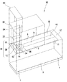
図2Aを参照すると、試験片100の別の例示的な実施形態が分解透視図で図示されている。試験片100は、基板105に設けられた複数の層を含む。これらの層は導電層150、試薬層122、スペーサー層160および親水性接着塗布が施された上部層180を含む。試験片100は導電層150および試薬層122が、例として米国特許出願公開番号US20050096409A1号および国際公開番号第WO2004040948A1号、同第WO2004040290A1、同第WO2004040287A1、同第WO2004040285A2、同第WO2004040005A1号、同第WO2004039897A2号、および同第WO2004039600A2号に説明されたスクリーン印刷プロセスを使用して基板105に順番に被着される一連の工程で製造される。別の実施形態では、インクジェット処理を使用して基板105に試薬層122が被着される。インクジェット処理は米国特許第6,179,979号に説明される。しかし、導電層150に試薬122を被着する別の処理には、ドロップオンデマンド処理が含まれる。スペーサー層160および上部層180はロールストックから取り出し、基板105にラミネート処理を施す。別の実施形態において、スパッタリング処理を導電層150に適用し、パターンが導電層150に形成される。レーザー剥離、レーザーエッチング、スクライブなどの機械的手段によって導電層150の10%未満、または一般には6%未満まで表面が剥がされる。試験片100は図1Aおよび1Bに示されるように遠端部103および近端部104を含む。
With reference to FIG. 2A, another exemplary embodiment of a
完全に組み立てられた試験片100は、図2Bに示されるようにインレット182を含み、このインレットから血液サンプルがサンプル受け入れチャンバー184に引き入れられる。インレット182は試験片100の遠位部分103を切削して形成される。血液サンプルをインレット182に適用して、サンプル受け入れチャンバー184を満たし、グルコースを測定することができる。試薬層122に隣接するスペーサー層160のU形開口部の側端はそれぞれサンプル受け入れチャンバー184の壁を定義する。サンプル受け入れチャンバー184の底部分または「フロア」は基板105と導電層150の一部を含む。サンプル受け入れチャンバー184の上部または「ルーフ」は遠位上部層180を含む。
The fully assembled
試験片90または100は、一般に均一な導電性材料の層が、好ましくはスパッタ被着で基板の全表面に被着される基板5を提供することによって製造される。次いで、レーザー剥離が導電パターン150を形成するために活用された。一技法では、レーザービームの移動を制御して「A1」、「A2」、「A3」、「A4」、「A4」、「A5」、「A6」などの剥離された隙間を含む電極パターンが、これらの隙間の距離を好ましくは50ミクロン以下、最も好ましくは約20ミクロンにして導電層に形成された。別の実施形態では、電極パターンを定義する開口部のあるマスクが剥離レーザーと基板と導電層の間に挿置され、十分な電力と強度で、例えば100ナノ秒未満にするなど適切な持続時間で導電層を剥離した。レーザー剥離のための様々な技法は、例としてErol C. Harveyらによる“Fabrication Techniques and Their Applications to Produce Novel Micromachined Structures and Devices Using Excimer Laser Projection”、Exitech Ltd., Hanborough Park, Long Hanborough, Oxford, UK, SPIE Vol. 3223, 1997で説明され、使用されるが、参照によって本明細書に組み込まれる。いずれの技法を使用しても、導電層150は、基準電極110、第1の作用電極112、第2の作用電極114、基準接着パッド111、第1の接着パッド113、第2の接着パッド115および試験片検出接着パッド117を含み、図A、2A、2Bに示されるように、導電層または金層に形成される。基準接着パッド111、第1の接着パッド113、第2の接着パッド115および試験片検出接着パッド117は試験測定器への電気的な接続を提供しデータおよび測定収集が行える。
The
導電層150は第1の隔離部分152、第2の隔離部分154および任意の第3の隔離部分156を含む。第1の隔離部分152および第2の隔離部分154は基板105の疎水性である露出表面積を最小にすることによって均一な試薬の塗布を促進する。第3の隔離部分156はいかなる形状(例えば三角形)であってもよく、毛管力を提供することにより試験片100の充填を促進し、サンプル受け入れチャンバー184に液体を引き入れる。第3の隔離部分156は、開口部159をも含み、これを介して導電層150と基板105に通じる。開口部159は、レーザーまたは機械的手段により穿孔して形成し得る。開口部159は試験片のすべてのコンポーネントをラミネートした後に作成され、こうすることで、組立てコストおよびエラーを低減できる。開口部159は約40マイクロメートルから約400マイクロメートルの好ましくは丸型の開口にする。
The
基準電極110と第1の隔離部分152の間の距離は、約2ミクロンから約50ミクロンであり、一般には約20ミクロンである。第1の隔離部分152と第1の作用電極112間の距離は約2ミクロンから約50ミクロンであり、一般には約20ミクロンである。同様に、第1の作用電極112と第2の隔離部分154間の距離、および第2の隔離部分154と第2の作用電極114間の距離は約2ミクロンから約50ミクロンであり、一般には20ミクロンである。また、第2の作用電極114と第3の隔離部分156の間の距離は、約2ミクロンから約50ミクロンであり、一般には約20ミクロンである。第1の隔離部分152と第2の隔離部分154の幅は一般に約120ミクロンから約200ミクロンである。導電性材料の約20ミクロンの幅ラインがレーザー剥離によって除去され、電極と隔離部分パターンが導電層150に形成される際、導電層150の10%未満が基板105から除去される。導電性材料を可能な限り少量除去することによって試験片電極に短絡回路を生じさせることなく基板105と導電層150間の表面エネルギーの差異を低減させる。このようにすることによって乾燥試薬22が導電層150によく接着する結果となり、試薬の塗布パターンと乾燥した試薬パッドの耐久性が制御され、それが利点である。
The distance between the
導電層50または150はさらに試験片100の遠端部103に耐静電気バー158を含む。試験片100に血液を充填中試験片100が患者に接触すると耐静電気バー158は導電層150へ静電荷を放散させる。耐静電気バー158は露出した疎水性の基板105の表面積を最小化することによって均一な試薬の塗布を促進し、毛管力を提供することにより試験片100の充填を促進し、サンプル受け入れチャンバー184に液体を引き入れる。
The
図2Aを再度参照すると、基準電極110、第1の作用電極112および第2の作用電極114は「トレース」と呼ばれる電極の拡張によって基準接着パッド111、第1の接着パッド113および第2の接着パッド115にそれぞれ接続される第1の作用電極トレース108は、第1の作用電極112から第1の接着パッド113まで電気的に導通がある経路を提供する。同様に、第2の作用電極トレース109は、第2の作用電極114から第2の接着パッド115まで電気的に導通がある経路を提供し、基準電極トレース107は、基準電極110から基準接着パッド111まで電気的に導通がある経路を提供する。
Referring again to FIG. 2A, the
導電層に使用され得る適切な材料は、Au、Pd、Ir、Pt、Rh、ステンレス鋼、添加酸化スズ、カーボンなどがある。一実施形態では、導電層の材料として米国特許第5,653,918号で説明されるようにカーボンインクが使用される。別の実施形態では導電層の材料として厚さ約15ナノメートルから約35ナノメートルの金またはパラジウムなどのスパッタ金属が使用される。導電層として金を使用する実施形態では、一般にスパッタ金を親水性材料とともに塗布し、試薬の塗布が促進される。例示的な親水性は、濃度約0.05%から約0.2%の2−メルカプトエタンスルホン酸ナトリウムを含む。均一な塗布を促進するために界面活性剤も親水性材料を含む金塗布溶液に追加される。例示的な界面活性剤には濃度約0.01%から約0.05%のプルロニック(Pluronic)F87および濃度約0.01%から約0.05%のプルロニック(Pluronic)P103が含まれる。 Suitable materials that can be used for the conductive layer include Au, Pd, Ir, Pt, Rh, stainless steel, added tin oxide, carbon, and the like. In one embodiment, carbon ink is used as the material for the conductive layer as described in US Pat. No. 5,653,918. In another embodiment, a sputter metal such as gold or palladium with a thickness of about 15 nanometers to about 35 nanometers is used as the material for the conductive layer. In embodiments where gold is used as the conductive layer, generally sputtered gold is applied with a hydrophilic material to facilitate application of the reagent. Exemplary hydrophilicity includes sodium 2-mercaptoethanesulfonate at a concentration of about 0.05% to about 0.2%. A surfactant is also added to the gold coating solution containing the hydrophilic material to promote uniform coating. Exemplary surfactants include Pluronic F87 at a concentration of about 0.01% to about 0.05% and Pluronic P103 at a concentration of about 0.01% to about 0.05%.
試薬層122は図2Aに示されるように基板105の導電層150の一部に設けられる。本発明の一実施形態では、試薬層122には選択的にグルコースに反応する酵素および希望するpHを維持するための緩衝剤などの化学物質が含まれる。本発明において使用に適した酵素の例として、グルコース・オキシダーゼまたはグルコース・デヒドロゲナーゼの何れかを含む。具体的には、グルコース・デヒドロゲナーゼはピロロキノリン・キノン補助因子(PQQとして省略され、一般にはメトキサチンと呼ばれる)を有する。他のグルコース脱水素酵素補助因子はニコチンアミド・アデニン・ジヌクレオチド(NADとして省略)またはフラビン・アデニン・ジヌクレオチド(FADとして省略)がある。使用に適切な媒介物質の例には、フェリシアニド(媒介物質フェリシアニド)または三塩化ルテニウムヘキサミン([RuIII(NH3)6]Cl3、ルテニウムヘキサミンと省略される場合がある)。様々な実施形態での使用に適切な緩衝剤の例として、りん酸またはシトラコン酸を含む。様々な実施形態での使用に適切な試薬配合物またはインクの例が米国特許第5,708,247号および同第6,046,051号、国際公開番号WO01/67099および同第WO01/73124号に見出される。
The
一実施形態では、配合物には、pHが約7のりん酸緩衝剤200mMおよび濃度範囲5%以上、好ましくは10%以上、さらに好ましくは、15%〜20%のルテニウムヘキサミン媒介物質が含まれる(媒介物質の重量÷緩衝剤容量に基づいたパーセント。)媒介物質としてルテニウムヘキサミンを使用するとき、グルコース・オキシダーゼはpH約7で十分高度な活性が得られることからpHを約7に選択した。ルテニウムヘキサミンの上限は溶解性に基づいた。ルテニウムヘキサミン濃度20%を超える酵素インクが配合される場合、ルテニウムヘキサミン固体粒子が試薬層22に存在し、試験中に溶解しなかった。未溶解のルテニウムヘキサミンが存在すると、試験片から試験片の精密性が低減する原因になると考えられている。酵素インクは、ルテニウムヘキサミン濃度を15%未満にして配合すると、試験電流値は低下した。ルテニウムヘキサミン濃度に少しでも変動があると試験電流値にばらつきが生じ、試験片間のばらつき度が高くなることから、一般に、試験電流値がルテニウムヘキサミン濃度に依存するのは好ましくない。
In one embodiment, the formulation includes 200 mM phosphate buffer at a pH of about 7 and a concentration range of 5% or more, preferably 10% or more, more preferably 15% to 20% of a ruthenium hexamine mediator. (Percentage based on mediator weight divided by buffer volume.) When using ruthenium hexamine as a mediator, glucose oxidase was chosen to have a pH of about 7 because sufficiently high activity was obtained at about pH7. The upper limit for ruthenium hexamine was based on solubility. When an enzyme ink with a ruthenium hexamine concentration exceeding 20% was blended, ruthenium hexamine solid particles were present in the
一実施形態では、配合物に酵素の活性が約1500ユニット/mLから約50000ユニット/mLの範囲になり、一般には、18000ユニット/mLである。酵素の活性範囲は、酵素の活性量が上記範囲内に入りグルコース電流が配合物の酵素の活性量に依存しないように選択される。生じたグルコース電流が酵素活性の小さなばらつきに左右されないことを確実にするため酵素の活性は十分に高くすべきである。例えば、酵素の活性が1500ユニット/mL未満の場合、グルコース電流は酵素の活性量に依存するであろう。一方、酵素の活性量が50000ユニット/mLを超える場合、溶解性の問題が生じ、グルコース・オキシダーゼは、配合物中で十分に溶解されない。さらに、配合物に酵素が多すぎると、試験片の価格が高くなってしまう。グルコース・オキシダーゼは、ビオザイム ラボラトリー インターナショナル リミテッド(Biozyme Laboratories International Limited)(米国カリフォルニア州サンディエゴ市所在)が販売している。グルコース・オキシダーゼは、酵素の活性が約250ユニット/mgであり、この酵素の活性ユニットは、pH7および25℃のo−ジアニシジン アッセイに基づく。
In one embodiment, the formulation has an enzyme activity ranging from about 1500 units / mL to about 50000 units / mL, generally 18000 units / mL. The enzyme activity range is selected such that the enzyme activity falls within the above range and the glucose current does not depend on the enzyme activity of the formulation. The enzyme activity should be sufficiently high to ensure that the resulting glucose current is not affected by small variations in enzyme activity. For example, if the activity of the enzyme is less than 1500 units / mL, the glucose current will depend on the amount of activity of the enzyme. On the other hand, if the enzyme activity exceeds 50000 units / mL, solubility problems arise and glucose oxidase is not sufficiently dissolved in the formulation. Furthermore, if there are too many enzymes in the formulation, the price of the specimen will be high. Glucose oxidase is sold by Biozyme Laboratories International Limited (San Diego, Calif.). Glucose oxidase has an enzyme activity of about 250 units / mg, which is based on the o-dianisidine assay at
任意的に、試薬層122は液体サンプルの存在下で試薬層122を導電層150の表面に保持するのに役立つマトリックス材料を含み、疎水性および親水性の両領域を有する。有益なマトリックス材料は、親水性粘土、カオリン、タルク、シリケート、けい藻土またはCab−o−Sil(登録商標) TS−610あるいはCab−o−Sil(登録商標) TS−530(米国ボストン所在のキャボット社(Cabot Corporation))などのシリカを含む。特定の理論に固執することを望まないが、サンプルの存在下でシリカがゲルネットワークを形成し、電極の表面で塗布を有効に維持すると考えられている。他の有益なマトリックス材料には、アルギン酸ソーダ、ポリエチレングリコール、ポリエチレンオキサイド、ポリビニルアルコール、ポリ酢酸ビニール、ポリマーラテックス材、ポリエーテルスルホン、アクリルおよびメタクリル酸ポリマー;澱粉、セルロースおよび他の天然多糖類(ポリアミド類またはコラーゲン)などのポリマー材が含まれる。有益な塗布製粉の一例は、米国特許第5,708,247号の実施例1で開示される。試薬層122は任意的にアルブミン、蔗糖、トレハロース、マンニトールまたはラクトースなど少なくとも1つの安定剤、粘性を調節するヒドロキシエチルセルロースなどの調節剤、DC1500などの消泡剤およびポリビニルピロリドンまたはポリビニルアルコールなど少なくとも1つの湿潤剤も含まれる。
Optionally,
例示的な実施形態では、試薬層122は電極の露出表面に対し層としても適用される。液体サンプルに接触する前の試薬層122の厚さは50ミクロンを超えず、通常的には20ミクロンを超えるべきではない。電極の表面に有効に塗布するには、層の厚さは約5ミクロン未満にすべきではなく、通常的には、約7ミクロン未満にしない。
In the exemplary embodiment,
図2Aにおいて、スペーサー層160は一般にポリエステルから形成され、熱シール接着剤または感圧接着剤で導電層150に接着される。
In FIG. 2A, the
上部層またはカバー180はスペーサー層160を完全に覆う。一実施形態では、上部層180は例えば、アドヒーシブリサーチ社(Adhesives Research Inc.)のARflow 90128などのような親水性接着剤でスペーサー層160に接着されるポリエステル材料である。上部層は、透明なポリエステルから形成され、サンプル受け入れチャンバー84が十分に満たされたかどうか使用者が視覚的に確認することができる。
The top layer or cover 180 completely covers the
本出願人は図1Aの同様なデザインに基づいたプロトタイプ(図3A)の試薬分布について別のデザイン(図3B)と比較した場合、より均一になる傾向があり、これによって試薬22への基板5の露出がより大きくなることを発見した。両プロトタイプは本明細書の図3Aおよび3Bに示される。図3Aおよび3Bの両プロトタイプは、同一の基板と導電材を使用して作成された。特に厚さ約0.18ミリメートル(約7ミル)の金スパッタのポリエステルフィルムロールがCPフィルムより、得られる。導電層(この場合、金)の厚さは約15ナノメートルであった。フィルムは縦横、約195mm X 27.5 mm のカード状に切断された。導電層はレーザースクライブまたは好ましくは、広域レーザー剥離、すなわちレーザーと基板の間に挿置されたマスク様の部材を使用しレーザー剥離の何れかを使用してパターン化され電極パターン層50が形成された。それぞれのプロトタイプの両表面は試薬の被着前にエアブラシ技法を使用してMESAおよび界面活性剤で処理された。特に両タイプの試験片に対し、導電層50は未処理であったか、0.1%の2−メルカプトエタンスルホン酸ナトリウム溶液(溶剤容量に対する化学物質の重量に基づいた%の濃度)と0.025%プルロニック(Pluronic)F87(またはMESA/F87)で1、2または4層が塗布され表面が親水性になったかの何れかであった。約1%のヒドロキシエチルセルロース、約10%の三塩化ルテニウムヘキサミン、約7.2%のグルコース・オキシダーゼ、約0.033%のプルロニック(Pluronic)P103、約0.017%のプルロニック(Pluronic)F87、およびpH6.9、約0.2Mの燐酸緩衝剤を含む試薬混合液が、例えばBioDotなどの適切な非接触ドロップオンデマンドシステムを使用して電極層に被着された。次いで、赤外線ヒーターを使用して約60℃で約3分間、カードの乾燥処理を行った。乾燥後、カードはスペーサーと親水性上面テープとともにラミネートされ、グルコース・センサーの配列を形成した。
Applicants tend to be more uniform when compared to another design (FIG. 3B) for the reagent distribution of a prototype (FIG. 3A) based on the similar design of FIG. I found that the exposure of became larger. Both prototypes are shown in FIGS. 3A and 3B herein. Both prototypes in FIGS. 3A and 3B were made using the same substrate and conductive material. In particular, a gold sputtered polyester film roll having a thickness of about 0.18 millimeters (about 7 mils) is obtained from the CP film. The thickness of the conductive layer (in this case gold) was about 15 nanometers. The film was cut into a card shape of about 195 mm × 27.5 mm in length and width. The conductive layer is patterned using either laser scribing or, preferably, wide area laser stripping, ie laser stripping using a mask-like member inserted between the laser and the substrate to form the
図3Aの第1のプロトタイプでは、電極10、12または14の何れかの端と近位の電気的に隔離されたアイランド52、54または56の端の間の隙間「A」は、約20ミクロンである。これとは対照的に、別のプロトタイプ(図3B)の隙間「B」は約200ミクロンであり、基板表面5はさらに露出することができる。隙間のスペースがA(〜20ミクロン)とB(〜200ミクロン)でこのように違うと、試薬が両方のプロトタイプの電極パターンに被着されたとき驚くべき結果が生じる。図3Aと3Bの両方を比較すると、この驚くべき結果が観察される。図3Bの試薬22と比較して、図3Aでは、試薬22がより均一になっていることが観察される。本出願人は、図3Aのプロトタイプでは除去する導電性材料の量を少なくすると、図3Bと比較した場合、下の基板の露出がより小さくなり表面がより均一になると考える。試薬の被着が均一になると分析物液体の分布の均一性が増すことも発見された。その結果、図3Aのプロトタイプに試薬が均一に分布されると分析物の測定プロセスの精度がより高くなると考えられる。
In the first prototype of FIG. 3A, the gap “A” between the end of either
実施例−精度の研究 Example-accuracy study
この前提を検証するため、図1A〜図1Cに示される電気的に隔離されたアイランド(“CI”)52および54のある試験片(または“CI試験片”)のプロトタイプを電気的に隔離されたアイランド52および54を含まない試験片(または非−CI試験片)のプロトタイプと比較して精度の研究を実施した。CI試験片の導電性のあるアイランド52および54の幅は140ミクロンであり、基準電極または作用電極10または12と導電性のあるアイランドの間の距離は30ミクロンだった。非−CI試験片では、電極間の距離は200ミクロンだった。
To verify this assumption, the prototype of the specimen with electrically isolated islands ("CI") 52 and 54 (or "CI specimen") shown in FIGS. 1A-1C is electrically isolated. A precision study was performed compared to a prototype of a specimen (or non-CI specimen) that did not contain the
試験片のバックグラウンド電流のみをテストするため、CI試験片と非−CI試験片の両方が試薬層22を除きすべての層とともに組み立てた。テストの方法は、オープン回路を2秒間、その後3秒間、400mVの電位を試験片に適用することを含む。2秒後に151mMのカリウム・フェリシアニド溶液(媒介物質フェリシアニド)/19mMのフェロシアン化カリウムを各試験片に適用し、5秒後に平均値が測定された。精度の結果(あるいは電流CV%)を表1に示す。
Both CI and non-CI specimens were assembled with all layers except
表1: 精度の結果

表1のデータは、非CI試験片と比較してCI試験片の電流のCV%が著しく改善されることを示す。 The data in Table 1 shows that the CV% of the current of the CI specimen is significantly improved compared to the non-CI specimen.
一般に図4を参照し、図1A〜図1C(または図2A〜図2B)に示される試験片90(または試験片100)は一般に測定器200または電気コネクタ202によって他の電気装置に連結され、接着パッド11、13、15、および17で試験片90の端部に接着パッドで接触して連結するように構成する。測定器200は一般に試験片90の電極用ポテンショスタットまたは他のコンポーネントを含み、電位および/または電流を提供する。測定器は、また試験片のシグナルから分析物の濃度を決定するためのプロセッサ(例:マイクロプロセッサまたはハードウェア)を含む。測定器は、また試験片のシグナルから決定した結果、例えば分析濃度、分析濃度の変動率、および/または分析濃度の閾値逸脱など(例としてhypoまたはhyperglycemia(低血糖症)を含む)表示する試験片ディスプレイ204を含む。
Referring generally to FIG. 4, the test strip 90 (or test strip 100) shown in FIGS. 1A-1C (or FIGS. 2A-2B) is generally connected to other electrical devices by a
本発明は、特定の実施形態および例示の図面に関して記載されてきたが、当業者は、本発明が記載された実施形態または図面に限定されないことを認識する。さらに、上記に記載される方法および工程は、特定の事象が特定の順序で生じることを示しているが、当業者は、特定の工程の順序が改変され得、そしてそのような改変は、本発明の実施形態に従って行われることを理解する。さらに、特定の工程は、可能である場合、並行したプロセスで同時に行われ得、そして上記のように連続して行われ得る。従って、特許請求の範囲に見いだされる本発明の開示または等価物の趣旨の中にある本発明の実施形態が存在する程度において、本発明がまた、これらの実施形態を網羅することが本発明者が意図するところである。最後に本明細書において引用されるすべての刊行物および特許文献は、本明細書において、その全体があたかも各個々の刊行物または特許出願が本明細書に具体的におよび個々に示されるかのごとく参考として援用される。 Although the present invention has been described with respect to particular embodiments and illustrative figures, those skilled in the art will recognize that the invention is not limited to the described embodiments or drawings. Furthermore, although the methods and steps described above indicate that certain events occur in a particular order, those skilled in the art can alter the order of particular steps, and such modifications are It will be understood that this is done according to embodiments of the invention. Further, certain steps can be performed simultaneously in parallel processes, if possible, and can be performed sequentially as described above. Therefore, to the extent that embodiments of the present invention exist within the spirit of the disclosure or equivalents of the present invention found in the claims, the present inventors also cover these embodiments. Is intended. Finally, all publications and patent documents cited herein are hereby incorporated by reference in their entirety as if each individual publication or patent application was specifically and individually indicated herein. It is used as a reference.
Claims (25)
第1の端部から第2の端部まで延在する略平坦な表面を有する基板と、
前記略平坦な表面に配設され、相互に離間した複数の電極を画定する導電性材料と、
前記複数の電極が電気的に導通しないように少なくとも2つの電極間に配設された導電性材料の隔離部分(isolated portion)と、を含む前記試験片。 A test specimen for analysis,
A substrate having a substantially flat surface extending from the first end to the second end;
A conductive material disposed on the substantially planar surface and defining a plurality of spaced apart electrodes;
An isolated portion of a conductive material disposed between at least two electrodes such that the plurality of electrodes are not electrically conductive.
前記測定器は、基準電極と作用電極の間に試験電圧を印加するための電気回路と、シグナルプロセッサとを有し、
前記試験片は、液体サンプルで前記試験片を満たす間、毛管現象が支援されるように導電性材料の隔離部分によって分離される基準電極と作用電極を有する基板を有する、測定システム。 An analyte measurement system for measuring an analyte concentration in a liquid sample comprising a measuring instrument and a test piece,
The measuring device has an electric circuit for applying a test voltage between a reference electrode and a working electrode, and a signal processor,
The test strip comprises a substrate having a reference electrode and a working electrode separated by an isolated portion of conductive material so that capillary action is supported while filling the test strip with a liquid sample.
基板と、
前記基板に配設した基準電極と、
前記基準電極に隣接して、前記基板に配設した第1の作用電極と、
前記第1の作用電極に隣接して、前記基板に配設した第2の作用電極と、
前記第1の作用電極と前記第2の作用電極の何れかの近位で、前記基準電極の遠位に配設した導電性材料の隔離部分と、を含む試験片。 A test strip for measuring an analyte concentration in a liquid sample,
A substrate,
A reference electrode disposed on the substrate;
A first working electrode disposed on the substrate adjacent to the reference electrode;
A second working electrode disposed on the substrate adjacent to the first working electrode;
A test strip comprising an isolated portion of a conductive material disposed distally of the reference electrode proximal to either the first working electrode or the second working electrode.
導電性材料の層を基板に被着するステップと、
導電性材料の層から選択した部分を除去して、導電性材料の少なくとも一つの電気的に隔離(electrically isolated)したアイランドを有する複数の電極を画定するステップと、を含み、
前記アイランドは、前記複数の電極の何れからも約50ミクロン以下の距離離間して、前記電極から前記アイランドを電気的に隔離する、方法。 A method of producing a test specimen for analysis,
Depositing a layer of conductive material on a substrate;
Removing selected portions from the layer of conductive material to define a plurality of electrodes having at least one electrically isolated island of conductive material; and
The island is separated from any of the plurality of electrodes by a distance of about 50 microns or less to electrically isolate the island from the electrode.
Applications Claiming Priority (1)
| Application Number | Priority Date | Filing Date | Title |
|---|---|---|---|
| US11/849,949 US7943022B2 (en) | 2007-09-04 | 2007-09-04 | Analyte test strip with improved reagent deposition |
Publications (1)
| Publication Number | Publication Date |
|---|---|
| JP2009063577A true JP2009063577A (en) | 2009-03-26 |
Family
ID=40010986
Family Applications (1)
| Application Number | Title | Priority Date | Filing Date |
|---|---|---|---|
| JP2008225762A Pending JP2009063577A (en) | 2007-09-04 | 2008-09-03 | Analytical test strip with improved reagent deposition |
Country Status (9)
| Country | Link |
|---|---|
| US (1) | US7943022B2 (en) |
| EP (1) | EP2034301B1 (en) |
| JP (1) | JP2009063577A (en) |
| CN (1) | CN101551355A (en) |
| AT (1) | ATE513203T1 (en) |
| AU (1) | AU2008207543B2 (en) |
| CA (1) | CA2639302C (en) |
| ES (1) | ES2365572T3 (en) |
| HK (1) | HK1129457A1 (en) |
Cited By (2)
| Publication number | Priority date | Publication date | Assignee | Title |
|---|---|---|---|---|
| JP2015535077A (en) * | 2012-10-17 | 2015-12-07 | ユニバーシティ オブ メリーランド, オフィス オブ テクノロジー コマーシャライゼーション | Device and method of using the device for detection of aminoacidopathy |
| JP2018036091A (en) * | 2016-08-30 | 2018-03-08 | アークレイ株式会社 | Biosensor and method of manufacturing the same |
Families Citing this family (64)
| Publication number | Priority date | Publication date | Assignee | Title |
|---|---|---|---|---|
| US6391005B1 (en) | 1998-03-30 | 2002-05-21 | Agilent Technologies, Inc. | Apparatus and method for penetration with shaft having a sensor for sensing penetration depth |
| US8641644B2 (en) | 2000-11-21 | 2014-02-04 | Sanofi-Aventis Deutschland Gmbh | Blood testing apparatus having a rotatable cartridge with multiple lancing elements and testing means |
| WO2002100254A2 (en) | 2001-06-12 | 2002-12-19 | Pelikan Technologies, Inc. | Method and apparatus for lancet launching device integrated onto a blood-sampling cartridge |
| US7981056B2 (en) | 2002-04-19 | 2011-07-19 | Pelikan Technologies, Inc. | Methods and apparatus for lancet actuation |
| US8337419B2 (en) | 2002-04-19 | 2012-12-25 | Sanofi-Aventis Deutschland Gmbh | Tissue penetration device |
| US9795747B2 (en) | 2010-06-02 | 2017-10-24 | Sanofi-Aventis Deutschland Gmbh | Methods and apparatus for lancet actuation |
| US9226699B2 (en) | 2002-04-19 | 2016-01-05 | Sanofi-Aventis Deutschland Gmbh | Body fluid sampling module with a continuous compression tissue interface surface |
| DE60238119D1 (en) | 2001-06-12 | 2010-12-09 | Pelikan Technologies Inc | ELECTRIC ACTUATOR ELEMENT FOR A LANZETTE |
| US9427532B2 (en) | 2001-06-12 | 2016-08-30 | Sanofi-Aventis Deutschland Gmbh | Tissue penetration device |
| ES2336081T3 (en) | 2001-06-12 | 2010-04-08 | Pelikan Technologies Inc. | SELF-OPTIMIZATION PUNCTURE DEVICE WITH MEANS OF ADAPTATION TO TEMPORARY VARIATIONS IN CUTANEOUS PROPERTIES. |
| US7025774B2 (en) | 2001-06-12 | 2006-04-11 | Pelikan Technologies, Inc. | Tissue penetration device |
| US9248267B2 (en) | 2002-04-19 | 2016-02-02 | Sanofi-Aventis Deustchland Gmbh | Tissue penetration device |
| US8784335B2 (en) | 2002-04-19 | 2014-07-22 | Sanofi-Aventis Deutschland Gmbh | Body fluid sampling device with a capacitive sensor |
| US9795334B2 (en) | 2002-04-19 | 2017-10-24 | Sanofi-Aventis Deutschland Gmbh | Method and apparatus for penetrating tissue |
| US7297122B2 (en) | 2002-04-19 | 2007-11-20 | Pelikan Technologies, Inc. | Method and apparatus for penetrating tissue |
| US8267870B2 (en) | 2002-04-19 | 2012-09-18 | Sanofi-Aventis Deutschland Gmbh | Method and apparatus for body fluid sampling with hybrid actuation |
| US8360992B2 (en) | 2002-04-19 | 2013-01-29 | Sanofi-Aventis Deutschland Gmbh | Method and apparatus for penetrating tissue |
| US7708701B2 (en) | 2002-04-19 | 2010-05-04 | Pelikan Technologies, Inc. | Method and apparatus for a multi-use body fluid sampling device |
| US7892183B2 (en) | 2002-04-19 | 2011-02-22 | Pelikan Technologies, Inc. | Method and apparatus for body fluid sampling and analyte sensing |
| US8372016B2 (en) | 2002-04-19 | 2013-02-12 | Sanofi-Aventis Deutschland Gmbh | Method and apparatus for body fluid sampling and analyte sensing |
| US7674232B2 (en) | 2002-04-19 | 2010-03-09 | Pelikan Technologies, Inc. | Method and apparatus for penetrating tissue |
| US7976476B2 (en) | 2002-04-19 | 2011-07-12 | Pelikan Technologies, Inc. | Device and method for variable speed lancet |
| US7175642B2 (en) | 2002-04-19 | 2007-02-13 | Pelikan Technologies, Inc. | Methods and apparatus for lancet actuation |
| US8221334B2 (en) | 2002-04-19 | 2012-07-17 | Sanofi-Aventis Deutschland Gmbh | Method and apparatus for penetrating tissue |
| US7901362B2 (en) | 2002-04-19 | 2011-03-08 | Pelikan Technologies, Inc. | Method and apparatus for penetrating tissue |
| US7491178B2 (en) | 2002-04-19 | 2009-02-17 | Pelikan Technologies, Inc. | Method and apparatus for penetrating tissue |
| US7547287B2 (en) | 2002-04-19 | 2009-06-16 | Pelikan Technologies, Inc. | Method and apparatus for penetrating tissue |
| US8579831B2 (en) | 2002-04-19 | 2013-11-12 | Sanofi-Aventis Deutschland Gmbh | Method and apparatus for penetrating tissue |
| US7229458B2 (en) | 2002-04-19 | 2007-06-12 | Pelikan Technologies, Inc. | Method and apparatus for penetrating tissue |
| US8702624B2 (en) | 2006-09-29 | 2014-04-22 | Sanofi-Aventis Deutschland Gmbh | Analyte measurement device with a single shot actuator |
| US7909778B2 (en) | 2002-04-19 | 2011-03-22 | Pelikan Technologies, Inc. | Method and apparatus for penetrating tissue |
| US9314194B2 (en) | 2002-04-19 | 2016-04-19 | Sanofi-Aventis Deutschland Gmbh | Tissue penetration device |
| US7232451B2 (en) * | 2002-04-19 | 2007-06-19 | Pelikan Technologies, Inc. | Method and apparatus for penetrating tissue |
| US7331931B2 (en) | 2002-04-19 | 2008-02-19 | Pelikan Technologies, Inc. | Method and apparatus for penetrating tissue |
| US8574895B2 (en) | 2002-12-30 | 2013-11-05 | Sanofi-Aventis Deutschland Gmbh | Method and apparatus using optical techniques to measure analyte levels |
| ATE476137T1 (en) | 2003-05-30 | 2010-08-15 | Pelikan Technologies Inc | METHOD AND DEVICE FOR INJECTING LIQUID |
| DK1633235T3 (en) | 2003-06-06 | 2014-08-18 | Sanofi Aventis Deutschland | Apparatus for sampling body fluid and detecting analyte |
| WO2006001797A1 (en) | 2004-06-14 | 2006-01-05 | Pelikan Technologies, Inc. | Low pain penetrating |
| EP1671096A4 (en) | 2003-09-29 | 2009-09-16 | Pelikan Technologies Inc | Method and apparatus for an improved sample capture device |
| EP1680014A4 (en) | 2003-10-14 | 2009-01-21 | Pelikan Technologies Inc | Method and apparatus for a variable user interface |
| US7822454B1 (en) | 2005-01-03 | 2010-10-26 | Pelikan Technologies, Inc. | Fluid sampling device with improved analyte detecting member configuration |
| EP1706026B1 (en) | 2003-12-31 | 2017-03-01 | Sanofi-Aventis Deutschland GmbH | Method and apparatus for improving fluidic flow and sample capture |
| US8828203B2 (en) | 2004-05-20 | 2014-09-09 | Sanofi-Aventis Deutschland Gmbh | Printable hydrogels for biosensors |
| WO2005120365A1 (en) | 2004-06-03 | 2005-12-22 | Pelikan Technologies, Inc. | Method and apparatus for a fluid sampling device |
| US9775553B2 (en) | 2004-06-03 | 2017-10-03 | Sanofi-Aventis Deutschland Gmbh | Method and apparatus for a fluid sampling device |
| US8652831B2 (en) | 2004-12-30 | 2014-02-18 | Sanofi-Aventis Deutschland Gmbh | Method and apparatus for analyte measurement test time |
| US9046480B2 (en) | 2006-10-05 | 2015-06-02 | Lifescan Scotland Limited | Method for determining hematocrit corrected analyte concentrations |
| WO2008040997A1 (en) * | 2006-10-05 | 2008-04-10 | Lifescan Scotland Limited | A test strip comprising patterned electrodes |
| WO2009126900A1 (en) | 2008-04-11 | 2009-10-15 | Pelikan Technologies, Inc. | Method and apparatus for analyte detecting device |
| US9375169B2 (en) | 2009-01-30 | 2016-06-28 | Sanofi-Aventis Deutschland Gmbh | Cam drive for managing disposable penetrating member actions with a single motor and motor and control system |
| US8965476B2 (en) | 2010-04-16 | 2015-02-24 | Sanofi-Aventis Deutschland Gmbh | Tissue penetration device |
| US20120122197A1 (en) * | 2010-11-12 | 2012-05-17 | Abner David Jospeh | Inkjet reagent deposition for biosensor manufacturing |
| CN102507688B (en) * | 2011-10-13 | 2014-03-12 | 中国科学院化学研究所 | Electrochemical biological sensor and preparation method and application thereof |
| US9535027B2 (en) * | 2012-07-25 | 2017-01-03 | Abbott Diabetes Care Inc. | Analyte sensors and methods of using same |
| US9121050B2 (en) | 2013-03-15 | 2015-09-01 | American Sterilizer Company | Non-enzyme based detection method for electronic monitoring of biological indicator |
| US8858884B2 (en) | 2013-03-15 | 2014-10-14 | American Sterilizer Company | Coupled enzyme-based method for electronic monitoring of biological indicator |
| US20160017399A1 (en) * | 2014-07-17 | 2016-01-21 | Lifescan Scotland Limited | Electrochemical-based analytical test strip with enzymatic reagent layer containing a naphthoquinone-based mediator and fad-gdh |
| CN204142671U (en) * | 2014-09-22 | 2015-02-04 | 英科新创(厦门)科技有限公司 | Electric pole type blood sugar examination bar |
| US10197522B2 (en) | 2015-03-18 | 2019-02-05 | Materion Corporation | Multilayer constructs for metabolite strips providing inert surface and mechanical advantage |
| US10378098B2 (en) | 2015-03-18 | 2019-08-13 | Materion Corporation | Methods for optimized production of multilayer metal/transparent conducting oxide (TCO) constructs |
| US20160290951A1 (en) * | 2015-03-31 | 2016-10-06 | Roche Diabetes Care, Inc. | Analyte meter with contoured strip port to improve electrochemical test strip reliability |
| GB201507506D0 (en) * | 2015-04-30 | 2015-06-17 | Inside Biometrics Ltd | Electrochemical test device |
| US10154809B2 (en) | 2015-06-24 | 2018-12-18 | University Of Virginia Patent Foundation | Test strip device and related methods thereof |
| CN108213719A (en) * | 2018-01-06 | 2018-06-29 | 武汉吉事达科技股份有限公司 | A kind of laser production method of multi-electrode blood sugar test paper |
Citations (6)
| Publication number | Priority date | Publication date | Assignee | Title |
|---|---|---|---|---|
| JPH11344462A (en) * | 1998-01-27 | 1999-12-14 | Matsushita Electric Ind Co Ltd | Method for determining substrate |
| JP2001305095A (en) * | 2000-04-25 | 2001-10-31 | Matsushita Electric Ind Co Ltd | Biosensor |
| WO2002086483A1 (en) * | 2001-04-16 | 2002-10-31 | Matsushita Electric Industrial Co., Ltd. | Biosensor |
| JP2003524162A (en) * | 2000-02-02 | 2003-08-12 | ライフスキャン・インコーポレイテッド | Electrochemical test strip for analyte measurement |
| JP2003254933A (en) * | 2002-03-01 | 2003-09-10 | Matsushita Electric Ind Co Ltd | Biosensor |
| JP2007524819A (en) * | 2003-06-20 | 2007-08-30 | エフ ホフマン−ラ ロッシュ アクチェン ゲゼルシャフト | System and method for code information on a biosensor test strip |
Family Cites Families (21)
| Publication number | Priority date | Publication date | Assignee | Title |
|---|---|---|---|---|
| JPS55117726A (en) | 1979-03-05 | 1980-09-10 | Hitachi Ltd | Manufacture of magnetic head |
| EP0699375B1 (en) | 1994-02-22 | 1997-07-09 | Koninklijke Philips Electronics N.V. | Laser etching method |
| AUPN661995A0 (en) | 1995-11-16 | 1995-12-07 | Memtec America Corporation | Electrochemical cell 2 |
| US5653918A (en) | 1996-01-11 | 1997-08-05 | E. I. Du Pont De Nemours And Company | Flexible thick film conductor composition |
| US5708247A (en) | 1996-02-14 | 1998-01-13 | Selfcare, Inc. | Disposable glucose test strips, and methods and compositions for making same |
| US6046051A (en) | 1997-06-27 | 2000-04-04 | Hemosense, Inc. | Method and device for measuring blood coagulation or lysis by viscosity changes |
| US6309526B1 (en) | 1997-07-10 | 2001-10-30 | Matsushita Electric Industrial Co., Ltd. | Biosensor |
| US5997817A (en) | 1997-12-05 | 1999-12-07 | Roche Diagnostics Corporation | Electrochemical biosensor test strip |
| US6338790B1 (en) * | 1998-10-08 | 2002-01-15 | Therasense, Inc. | Small volume in vitro analyte sensor with diffusible or non-leachable redox mediator |
| US7073246B2 (en) | 1999-10-04 | 2006-07-11 | Roche Diagnostics Operations, Inc. | Method of making a biosensor |
| CN100363739C (en) * | 1999-11-15 | 2008-01-23 | 松下电器产业株式会社 | Biosensor, method of forming thin-film electrode, and method and apparatus for quantitative determination |
| GB0005564D0 (en) | 2000-03-08 | 2000-05-03 | Inverness Medical Ltd | Measurjement of substances in liquid |
| DE60112733T2 (en) | 2000-03-28 | 2006-06-01 | Diabetes Diagnostics, Inc., Waltham | Fast-acting glucose sensor |
| EP1426757B9 (en) | 2001-09-14 | 2012-01-25 | ARKRAY, Inc. | Method, tool and device for measuring concentration |
| WO2003029804A1 (en) * | 2001-09-28 | 2003-04-10 | Arkray, Inc. | Measurement instrument and concentration measurement apparatus |
| PT1578612E (en) | 2002-10-30 | 2007-03-30 | Lifescan Scotland Ltd | Continuous web process for the manufacture of electrochemical sensors |
| ES2290507T3 (en) | 2002-10-30 | 2008-02-16 | Lifescan Scotland Ltd | REFRIGERATION STATIONS FOR USE IN A COIL PRINTING PROCESS FOR THE MANUFACTURE OF ELECTROMECHANICAL SENSORS. |
| JP4352152B2 (en) | 2002-12-02 | 2009-10-28 | アークレイ株式会社 | Analysis tool |
| US20060231396A1 (en) | 2002-12-20 | 2006-10-19 | Hideaki Yamaoka | Thin analyzing device |
| EP1642125B1 (en) * | 2003-06-20 | 2017-09-27 | Roche Diabetes Care GmbH | Biosensor with multiple electrical functionalities |
| US8066866B2 (en) | 2005-10-17 | 2011-11-29 | Lifescan, Inc. | Methods for measuring physiological fluids |
-
2007
- 2007-09-04 US US11/849,949 patent/US7943022B2/en active Active
-
2008
- 2008-08-27 AU AU2008207543A patent/AU2008207543B2/en not_active Ceased
- 2008-09-03 CA CA2639302A patent/CA2639302C/en not_active Expired - Fee Related
- 2008-09-03 JP JP2008225762A patent/JP2009063577A/en active Pending
- 2008-09-04 AT AT08252946T patent/ATE513203T1/en not_active IP Right Cessation
- 2008-09-04 EP EP08252946A patent/EP2034301B1/en not_active Not-in-force
- 2008-09-04 ES ES08252946T patent/ES2365572T3/en active Active
- 2008-09-04 CN CNA2008102127425A patent/CN101551355A/en active Pending
-
2009
- 2009-08-12 HK HK09107434.0A patent/HK1129457A1/en not_active IP Right Cessation
Patent Citations (6)
| Publication number | Priority date | Publication date | Assignee | Title |
|---|---|---|---|---|
| JPH11344462A (en) * | 1998-01-27 | 1999-12-14 | Matsushita Electric Ind Co Ltd | Method for determining substrate |
| JP2003524162A (en) * | 2000-02-02 | 2003-08-12 | ライフスキャン・インコーポレイテッド | Electrochemical test strip for analyte measurement |
| JP2001305095A (en) * | 2000-04-25 | 2001-10-31 | Matsushita Electric Ind Co Ltd | Biosensor |
| WO2002086483A1 (en) * | 2001-04-16 | 2002-10-31 | Matsushita Electric Industrial Co., Ltd. | Biosensor |
| JP2003254933A (en) * | 2002-03-01 | 2003-09-10 | Matsushita Electric Ind Co Ltd | Biosensor |
| JP2007524819A (en) * | 2003-06-20 | 2007-08-30 | エフ ホフマン−ラ ロッシュ アクチェン ゲゼルシャフト | System and method for code information on a biosensor test strip |
Cited By (3)
| Publication number | Priority date | Publication date | Assignee | Title |
|---|---|---|---|---|
| JP2015535077A (en) * | 2012-10-17 | 2015-12-07 | ユニバーシティ オブ メリーランド, オフィス オブ テクノロジー コマーシャライゼーション | Device and method of using the device for detection of aminoacidopathy |
| JP2018036091A (en) * | 2016-08-30 | 2018-03-08 | アークレイ株式会社 | Biosensor and method of manufacturing the same |
| US10619178B2 (en) | 2016-08-30 | 2020-04-14 | Arkray, Inc. | Biosensor and production method for same |
Also Published As
| Publication number | Publication date |
|---|---|
| HK1129457A1 (en) | 2009-11-27 |
| ES2365572T3 (en) | 2011-10-07 |
| AU2008207543B2 (en) | 2014-01-16 |
| CA2639302C (en) | 2017-09-19 |
| US20090057146A1 (en) | 2009-03-05 |
| US7943022B2 (en) | 2011-05-17 |
| EP2034301B1 (en) | 2011-06-15 |
| CN101551355A (en) | 2009-10-07 |
| EP2034301A3 (en) | 2010-01-13 |
| CA2639302A1 (en) | 2009-03-04 |
| ATE513203T1 (en) | 2011-07-15 |
| AU2008207543A1 (en) | 2009-03-19 |
| EP2034301A2 (en) | 2009-03-11 |
Similar Documents
| Publication | Publication Date | Title |
|---|---|---|
| JP2009063577A (en) | Analytical test strip with improved reagent deposition | |
| JP5044655B2 (en) | Reagent formulations using ruthenium hexamine as a transmitter for electrochemical test strips | |
| US7875461B2 (en) | Test strip and connector | |
| JP4879459B2 (en) | Electrochemical biosensor strip for analysis of liquid samples | |
| US10859525B2 (en) | Analyte sensors and methods of using same | |
| JP5185044B2 (en) | System and method for discriminating a control solution from a physiological sample | |
| JP2003521708A (en) | Electrochemical method and apparatus used for measurement of analyte concentration with corrected hematocrit value | |
| JP6081414B2 (en) | Low total salt reagent compositions and systems for biosensors | |
| US20150362501A1 (en) | Biosensor and process for producing same | |
| JP2011099849A (en) | Dual-chamber multi-analyte test strip including counter electrode | |
| TW200815752A (en) | Methods for fabricating a biosensor with a surface texture | |
| KR20140137410A (en) | Test strip with stacked unidirectional contact | |
| JP2014224828A5 (en) | ||
| KR20190091569A (en) | Test element for electrochemically detecting at least one analyte | |
| KR20150111981A (en) | Electrochemical-based analytical test strip with soluble acidic material coating | |
| TW201522962A (en) | Electrochemical-based analytical test strip with ultra-thin discontinuous metal layer | |
| WO2015178912A1 (en) | Analyte sensors and methods of using same |
Legal Events
| Date | Code | Title | Description |
|---|---|---|---|
| A621 | Written request for application examination |
Free format text: JAPANESE INTERMEDIATE CODE: A621 Effective date: 20110715 |
|
| A131 | Notification of reasons for refusal |
Free format text: JAPANESE INTERMEDIATE CODE: A131 Effective date: 20120828 |
|
| A977 | Report on retrieval |
Free format text: JAPANESE INTERMEDIATE CODE: A971007 Effective date: 20120830 |
|
| A521 | Request for written amendment filed |
Free format text: JAPANESE INTERMEDIATE CODE: A523 Effective date: 20121127 |
|
| A02 | Decision of refusal |
Free format text: JAPANESE INTERMEDIATE CODE: A02 Effective date: 20130521 |