JP2009044599A - Method of manufacturing case, piezoelectric vibrator, oscillator, electronic device, and radio clock - Google Patents
Method of manufacturing case, piezoelectric vibrator, oscillator, electronic device, and radio clock Download PDFInfo
- Publication number
- JP2009044599A JP2009044599A JP2007209102A JP2007209102A JP2009044599A JP 2009044599 A JP2009044599 A JP 2009044599A JP 2007209102 A JP2007209102 A JP 2007209102A JP 2007209102 A JP2007209102 A JP 2007209102A JP 2009044599 A JP2009044599 A JP 2009044599A
- Authority
- JP
- Japan
- Prior art keywords
- case
- piezoelectric vibrator
- manufacturing
- ring
- lead
- Prior art date
- Legal status (The legal status is an assumption and is not a legal conclusion. Google has not performed a legal analysis and makes no representation as to the accuracy of the status listed.)
- Granted
Links
Images


Classifications
-
- H—ELECTRICITY
- H03—ELECTRONIC CIRCUITRY
- H03H—IMPEDANCE NETWORKS, e.g. RESONANT CIRCUITS; RESONATORS
- H03H9/00—Networks comprising electromechanical or electro-acoustic devices; Electromechanical resonators
- H03H9/02—Details
- H03H9/05—Holders; Supports
- H03H9/10—Mounting in enclosures
- H03H9/1007—Mounting in enclosures for bulk acoustic wave [BAW] devices
- H03H9/1014—Mounting in enclosures for bulk acoustic wave [BAW] devices the enclosure being defined by a frame built on a substrate and a cap, the frame having no mechanical contact with the BAW device
- H03H9/1021—Mounting in enclosures for bulk acoustic wave [BAW] devices the enclosure being defined by a frame built on a substrate and a cap, the frame having no mechanical contact with the BAW device the BAW device being of the cantilever type
-
- H—ELECTRICITY
- H01—ELECTRIC ELEMENTS
- H01L—SEMICONDUCTOR DEVICES NOT COVERED BY CLASS H10
- H01L2224/00—Indexing scheme for arrangements for connecting or disconnecting semiconductor or solid-state bodies and methods related thereto as covered by H01L24/00
- H01L2224/01—Means for bonding being attached to, or being formed on, the surface to be connected, e.g. chip-to-package, die-attach, "first-level" interconnects; Manufacturing methods related thereto
- H01L2224/42—Wire connectors; Manufacturing methods related thereto
- H01L2224/44—Structure, shape, material or disposition of the wire connectors prior to the connecting process
- H01L2224/45—Structure, shape, material or disposition of the wire connectors prior to the connecting process of an individual wire connector
- H01L2224/45001—Core members of the connector
- H01L2224/45099—Material
- H01L2224/451—Material with a principal constituent of the material being a metal or a metalloid, e.g. boron (B), silicon (Si), germanium (Ge), arsenic (As), antimony (Sb), tellurium (Te) and polonium (Po), and alloys thereof
- H01L2224/45138—Material with a principal constituent of the material being a metal or a metalloid, e.g. boron (B), silicon (Si), germanium (Ge), arsenic (As), antimony (Sb), tellurium (Te) and polonium (Po), and alloys thereof the principal constituent melting at a temperature of greater than or equal to 950°C and less than 1550°C
- H01L2224/45144—Gold (Au) as principal constituent
-
- H—ELECTRICITY
- H01—ELECTRIC ELEMENTS
- H01L—SEMICONDUCTOR DEVICES NOT COVERED BY CLASS H10
- H01L2224/00—Indexing scheme for arrangements for connecting or disconnecting semiconductor or solid-state bodies and methods related thereto as covered by H01L24/00
- H01L2224/01—Means for bonding being attached to, or being formed on, the surface to be connected, e.g. chip-to-package, die-attach, "first-level" interconnects; Manufacturing methods related thereto
- H01L2224/42—Wire connectors; Manufacturing methods related thereto
- H01L2224/47—Structure, shape, material or disposition of the wire connectors after the connecting process
- H01L2224/48—Structure, shape, material or disposition of the wire connectors after the connecting process of an individual wire connector
- H01L2224/4805—Shape
- H01L2224/4809—Loop shape
- H01L2224/48091—Arched
-
- Y—GENERAL TAGGING OF NEW TECHNOLOGICAL DEVELOPMENTS; GENERAL TAGGING OF CROSS-SECTIONAL TECHNOLOGIES SPANNING OVER SEVERAL SECTIONS OF THE IPC; TECHNICAL SUBJECTS COVERED BY FORMER USPC CROSS-REFERENCE ART COLLECTIONS [XRACs] AND DIGESTS
- Y10—TECHNICAL SUBJECTS COVERED BY FORMER USPC
- Y10T—TECHNICAL SUBJECTS COVERED BY FORMER US CLASSIFICATION
- Y10T29/00—Metal working
- Y10T29/42—Piezoelectric device making
Landscapes
- Physics & Mathematics (AREA)
- Acoustics & Sound (AREA)
- Piezo-Electric Or Mechanical Vibrators, Or Delay Or Filter Circuits (AREA)
- Shaping Metal By Deep-Drawing, Or The Like (AREA)
- Oscillators With Electromechanical Resonators (AREA)
Abstract
Description
本発明は、圧電振動片を備えてなる圧電振動子において前記圧電振動片を収容するケースの製造方法、及びこの方法によって得られたケースを備える圧電振動子と、この圧電振動子を備えた発振器、電子機器、及び電波時計に関する。 The present invention relates to a method for manufacturing a case for accommodating the piezoelectric vibrating piece in a piezoelectric vibrator including the piezoelectric vibrating piece, a piezoelectric vibrator including a case obtained by the method, and an oscillator including the piezoelectric vibrator. The present invention relates to electronic devices and radio clocks.
近年、携帯電話や携帯情報端末器には、時刻源や制御信号のタイミング源、リファレンス信号源などとして、水晶などを利用した圧電振動子が用いられている。この種の圧電振動子は、様々なものが提供されているが、その1つとして、略円筒状に形成されたシリンダーパッケージタイプの圧電振動子が知られている。 In recent years, a piezoelectric vibrator using a crystal or the like is used as a time source, a timing source of a control signal, a reference signal source, or the like in a mobile phone or a portable information terminal. Various types of piezoelectric vibrators of this type are provided, and as one of them, a cylinder package type piezoelectric vibrator formed in a substantially cylindrical shape is known.
このようなシリンダーパッケージタイプの圧電振動子は、圧電振動片を気密に封止するケースの開口部側から2本のリードを突出させることで、圧電振動片の両面に設けられた励振電極のそれぞれと外部との接続を可能としている。
ところで、この種の圧電振動子は各種の電子機器等に搭載されるが、これら電子機器等は年々小型化が進んでいるため、圧電振動子においても、さらなる小型化が求められている。圧電振動子の小型化を図るためには、リングの外径を小さくすることが有効である。そのためには、2本のリードの径を細くする必要がある。ところが、リードを現状よりもさらに細くした場合には、剛性が低下してしまうので、製造途中で変形してしまうおそれがあった。特に、インナーリード部よりも長さのあるアウターリード部が変形し易いものであった。アウターリード部が変形してしまうと、互いの平行度が保てなくなってしまうため、品質が低下し、製品として使用できなくなってしまう。その結果、歩留まりの低下を招く可能性があった。
In such a cylinder package type piezoelectric vibrator, each of the excitation electrodes provided on both surfaces of the piezoelectric vibrating piece is formed by projecting two leads from the opening side of the case that hermetically seals the piezoelectric vibrating piece. And connection to the outside.
By the way, this type of piezoelectric vibrator is mounted on various electronic devices and the like. However, since these electronic devices and the like have been downsized year by year, further downsizing of piezoelectric vibrators is also required. In order to reduce the size of the piezoelectric vibrator, it is effective to reduce the outer diameter of the ring. For this purpose, it is necessary to reduce the diameter of the two leads. However, when the lead is made thinner than the current state, the rigidity is lowered, and there is a possibility that the lead may be deformed during the manufacturing. In particular, the outer lead portion that is longer than the inner lead portion is easily deformed. If the outer lead portion is deformed, the parallelism between the outer leads cannot be maintained, so that the quality is lowered and the product cannot be used. As a result, there is a possibility that the yield is reduced.
また、製造途中で、アウターリード部が他の気密端子のアウターリード部と絡み合ってしまい、生産ラインを一時的に停止させるおそれもあり、この点においても、歩留まりの低下を招く可能性があった。特に、小型化を目指すほど、前述した問題が顕著に発生するおそれがあった。そのため、現状の製造方法では、歩留まり良く、高品質でさらなる小型化を図った圧電振動子を製造することが困難である。 In addition, during manufacture, the outer lead part may be entangled with the outer lead part of another hermetic terminal, which may temporarily stop the production line. In this respect as well, the yield may be reduced. . In particular, as the size is reduced, the above-described problem may occur more remarkably. Therefore, with the current manufacturing method, it is difficult to manufacture a piezoelectric vibrator with high yield and high quality and further miniaturization.
そこで、2本のリードではなく、1本のリードからなる圧電振動子が提供されている(特許文献1参照)。すなわち、この圧電振動子では、リードとケース(金属キャップ)とを一対の端子とすることで、従来では2本のリードをケースの開口部から突出させていたのに対し、1本のリードのみを突出させるようにしている。
ところで、特許文献1の圧電振動子では、例えばケース(金属キャップ)に金属端子を取り付けることで外部との電気的接続を容易にしているが、このようにケースに金属端子を接続する場合、通常ははんだによって接続を行う。しかしながら、ケースを導電性にするべく、これを金属製にしているため、このケースは熱容量が大きくなっている。したがって、ケースに金属端子をはんだ付けする際にケース全体をある程度加熱する必要があり、そのため、このはんだ付けの処理が難しくなっており、圧電振動子自体の製造の容易化を妨げる一因になっている。
By the way, in the piezoelectric vibrator of
本発明は前記事情に鑑みてなされたもので、特に端子部を有するケースを容易に製造できるようにしたケースの製造方法と、この方法によって得られたケースを備える圧電振動子、さらにこの圧電振動子を備えた発振器、電子機器、及び電波時計を提供することを目的としている。 The present invention has been made in view of the above circumstances, and in particular, a method for manufacturing a case that can easily manufacture a case having a terminal portion, a piezoelectric vibrator including the case obtained by this method, and the piezoelectric vibration An object is to provide an oscillator, an electronic device, and a radio timepiece having a child.
上記課題を解決するために、この発明は以下の手段を提案している。
本発明のケースの製造方法は、圧電振動片を備えてなる圧電振動子において前記圧電振動片を収容するケースの製造方法であって、導電材料からなる板材に深絞り加工を行い、前記板材を略有底円筒状に加工する深絞り工程と、前記深絞り工程で略有底円筒状に加工された板材の底部の外面を、該底部の外径より小さい内径の凹部あるいは孔を有するダイの、前記凹部あるいは孔の開口部を含む面に当接させつつ、該板材の底部の内面をパンチで押圧して段絞り加工を行うことにより、該底部の外面に突起部を形成する段絞り工程と、前記段絞り工程で突起部を形成した略有底円筒状の板材を、その開口部側の所定の位置で切断することにより、突起部を有する略有底円筒状のケースを得る切断工程と、を備えたことを特徴としている。
In order to solve the above problems, the present invention proposes the following means.
The case manufacturing method of the present invention is a method for manufacturing a case that accommodates the piezoelectric vibrating piece in a piezoelectric vibrator including the piezoelectric vibrating piece, and performs deep drawing on a plate made of a conductive material. A deep drawing step of processing into a substantially bottomed cylindrical shape, and a die having a recess or a hole having an inner diameter smaller than the outer diameter of the bottom portion of the outer surface of the bottom of the plate material processed into a substantially bottomed cylindrical shape in the deep drawing step. A step drawing process for forming a protrusion on the outer surface of the bottom by pressing the inner surface of the bottom of the plate with a punch while making contact with a surface including the opening of the recess or hole. And a cutting step of obtaining a substantially bottomed cylindrical case having a protruding portion by cutting the substantially bottomed cylindrical plate material having the protruding portion formed in the step-drawing step at a predetermined position on the opening side. It is characterized by having.
このケースの製造方法によれば、深絞り工程と段絞り工程とを経ることにより、略有底円筒状に加工した板材の底部外面に突起部を形成することができる。そして、切断工程を経ることにより、突起部を有する略有底円筒状のケースを得ることができる。したがって、この突起部を端子部として機能させることにより、従来のようなはんだ付けを行う工程が不要になる。 According to this case manufacturing method, the projecting portion can be formed on the outer surface of the bottom portion of the plate material processed into a substantially bottomed cylindrical shape through the deep drawing step and the step drawing step. And a substantially bottomed cylindrical case having a protrusion can be obtained through the cutting step. Therefore, by making this protrusion function as a terminal portion, a conventional soldering process becomes unnecessary.
また、前記ケースの製造方法においては、前記段絞り工程で前記突起部の長さを所望の長さより長くなるように形成し、前記段絞り工程の後に、前記突起部の長さを所望の長さに調整する調整工程を有しているのが好ましい。
このようにすれば、ケースを量産した際、突起部の長さがばらつくことなく、所望の長さに均一に揃うようになる。
Further, in the case manufacturing method, the length of the protrusion is formed to be longer than a desired length in the step drawing process, and the length of the protrusion is set to a desired length after the step drawing process. It is preferable to have an adjusting step for adjusting the thickness.
If it does in this way, when a case is mass-produced, the length of a projection part will come to match uniformly in desired length, without varying.
また、前記ケースの製造方法においては、前記調整工程では、前記所望の長さに対応する所望の深さで所定の内径を有する穴部を有したダイを用い、前記の所望の長さより長い突起部を前記穴部に挿入し、その状態で前記板材の底部の内面をパンチで押圧することにより、前記突起部を所望の長さに圧縮するのが好ましい。
このようにすれば、突起部を圧縮することでその長さを所望の長さにすることができるとともに、その太さをダイの内径に揃えることができ、したがって得られる突起部の長さと外径を予め設定した寸法に容易に調整することができる。
In the case manufacturing method, the adjustment step uses a die having a hole having a predetermined inner diameter at a desired depth corresponding to the desired length, and a protrusion longer than the desired length. It is preferable that the protrusion is compressed to a desired length by inserting a portion into the hole and pressing the inner surface of the bottom of the plate with a punch in that state.
In this way, the length of the protrusion can be reduced to the desired length by compressing the protrusion, and the thickness can be matched to the inner diameter of the die. The diameter can be easily adjusted to a preset size.
また、前記ケースの製造方法においては、前記板材が複数個のケースを形成するための連続した帯状のものであるのが好ましい。
このようにすれば、帯状の保持材をその長さ方向に移動させつつ、各工程で順次処理を行うことにより、ケースの製造を高効率(高速)で自動化することができる。
Moreover, in the manufacturing method of the case, it is preferable that the plate material has a continuous band shape for forming a plurality of cases.
If it does in this way, manufacture of a case can be automated with high efficiency (high speed) by performing processing sequentially in each process, moving a beltlike holding material in the length direction.
また、前記ケースの製造方法においては、前記板材はメッキ処理後のものであるのが好ましい。
このようにすれば、前記の深絞り工程や段絞り工程を経ることによってメッキ処理済みのケースが得られ、したがって得られたケースを個々にメッキ処理する場合に比べ、メッキ処理の効率化、容易化を図ることができる。
また、前記ケースの製造方法においては、前記板材は厚さが0.12mmのものであるのが好ましい。
Moreover, in the manufacturing method of the case, it is preferable that the plate material is after plating.
In this way, a case having been plated is obtained through the deep drawing step and the step drawing step, and therefore, the plating case is made more efficient and easier than when the obtained cases are individually plated. Can be achieved.
In the case manufacturing method, the plate member preferably has a thickness of 0.12 mm.
本発明の圧電振動子は、圧電振動片と、開口部を有し、前記圧電振動片を内部に収納するケースと、環状のリングと、該リングを貫通した状態で配置され、リングを間に挟んで一端側が前記圧電振動片に電気的に接続されるインナーリード部とされ、他端側が外部に電気的に接続されるアウターリード部とされた1本のリードと、該リードと前記リングとを固定させる充填材とを有し、前記ケース内を密閉させる気密端子と、を備えた圧電振動子であって、前記ケースが、前記の製造方法で得られたものであることを特徴としている。
この圧電振動子によれば、突起部を有する略有底円筒状のケースが、はんだ付けを行うことなく製造されており、したがってその製造が容易になっているので、この圧電振動子自体もその製造の容易化が図られたものとなる。
また、導電材料からなるケースに突起部を設けたので、このケースの突起部と1本のリードとを一対の端子にすることができる。よって、リードを1本にしたことで、リングの外径を小さくしても2本の場合に比べてリードの径を細くする必要がなく、さらに、製造途中で他のものと絡み合うおそれも少ないため、圧電振動子自体の小型化が可能になる。
A piezoelectric vibrator according to the present invention includes a piezoelectric vibrating piece, an opening, a case that accommodates the piezoelectric vibrating piece therein, an annular ring, and a state that penetrates the ring. One lead with one end side electrically connected to the piezoelectric vibrating piece and the other end side being an outer lead portion electrically connected to the outside, the lead and the ring And a hermetic terminal for sealing the inside of the case, wherein the case is obtained by the manufacturing method. .
According to this piezoelectric vibrator, the substantially bottomed cylindrical case having the protrusions is manufactured without soldering, and thus the manufacture thereof is facilitated. This facilitates manufacturing.
In addition, since the projecting portion is provided in the case made of the conductive material, the projecting portion of the case and one lead can be used as a pair of terminals. Therefore, by using one lead, even if the outer diameter of the ring is reduced, there is no need to make the lead diameter smaller than in the case of two rings, and there is less risk of entanglement with other parts during the manufacturing process. Therefore, the piezoelectric vibrator itself can be reduced in size.
また、本発明の発振器は、前記の圧電振動子が発振子として集積回路に接続されていることを特徴としている。
また、本発明の電子機器は、前記の圧電振動子を備えることを特徴としている。
また、本発明の電波時計は、前記の圧電振動子が、フィルタ部に電気的に接続されていることを特徴としている。
The oscillator according to the present invention is characterized in that the piezoelectric vibrator is connected to an integrated circuit as an oscillator.
In addition, an electronic apparatus according to the present invention includes the above-described piezoelectric vibrator.
The radio timepiece of the present invention is characterized in that the piezoelectric vibrator is electrically connected to a filter portion.
この発明に係る発振器、電子機器、電波時計によれば、製造の容易化が図られ、さらに小型化が可能な圧電振動子を備えているので、これら発振器、電子機器、電波時計自体もその製造の容易化が図られたものとなり、また小型化が可能なものとなる。 According to the oscillator, the electronic device, and the radio timepiece according to the present invention, since the manufacture of the oscillator is facilitated and the piezoelectric vibrator that can be further downsized is provided, the oscillator, the electronic device, and the radio timepiece itself are also manufactured. Thus, it is possible to facilitate the reduction of the size.
本発明のケースの製造方法によれば、はんだ付けを行うことなく、ケースに突起部を一体に形成するようにしたので、特に突起部についての製造工程を容易にすることができる。
本発明の圧電振動子によれば、製造が容易なケースを用いているので、この圧電振動子自体もその製造の容易化が図られたものとなり、さらに、リードを1本にしているので、圧電振動子自体の小型化が可能なものとなる。
本発明の発振器、電子機器、及び、電波時計によれば、製造の容易化が図られ、さらに小型化が可能な圧電振動子を備えているので、これら発振器、電子機器、電波時計自体もその製造の容易化が図られたものとなり、また小型化が可能なものとなる。
According to the manufacturing method of the case of the present invention, since the protrusion is integrally formed on the case without performing soldering, the manufacturing process for the protrusion can be facilitated.
According to the piezoelectric vibrator of the present invention, since a case that is easy to manufacture is used, the piezoelectric vibrator itself is also easy to manufacture, and furthermore, since there is one lead, The piezoelectric vibrator itself can be downsized.
According to the oscillator, the electronic device, and the radio timepiece of the present invention, the piezoelectric vibrator is provided that can be manufactured easily and can be further downsized. Manufacturing is facilitated and downsizing is possible.
(第1の実施形態)
図1から図3は、本発明に係る圧電振動子の第1の実施形態を示す図であり、図1は本実施形態の圧電振動子の全体を示す側断面図、図2は図1のA−A線矢視断面図、図3は図1のB−B線矢視断面図である。
(First embodiment)
1 to 3 are views showing a first embodiment of a piezoelectric vibrator according to the present invention, FIG. 1 is a side sectional view showing the whole of the piezoelectric vibrator of the present embodiment, and FIG. AA arrow sectional drawing, FIG. 3 is BB arrow sectional drawing of FIG.
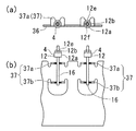
図1から図3に示すように本実施形態の圧電振動子1は、シリンダーパッケージタイプの圧電振動子であって、圧電振動片2と、この圧電振動片2を内部に配してその外周を覆う有底略円筒状のケース3と、ケース3の開口部3aを気密に封止する気密端子4と、を備えて構成されたものである。圧電振動片2は、本実施形態では音叉型の振動片であり、隣接した状態で互いに平行に配設された一対の振動腕部5、6と、振動腕部5、6の基端側を一体的に固定する基部7とを備えた略板状の水晶片2aで形成されている。また、水晶片2aの両面には、それぞれ、クロム(Cr)、ニッケル(Ni)、アルミニウム(Al)やチタン(Ti)などの導電性膜が所定のパターンに形成されて、第一の励振電極8、及び第二の励振電極9が設けられている。第一の励振電極8と第二の励振電極9とは、互いに電気的に切り離されてパターニングされている。
As shown in FIGS. 1 to 3, the
そして、第一の励振電極8及び第二の励振電極9のそれぞれに電圧を印加することにより、振動腕部5、6を互いに接近させあるいは離間させる方向に、所定の共振周波数で振動させることが可能になっている。なお、振動腕部5、6の先端側において、第一の励振電極8および第二の励振電極9の少なくとも一方には、クロム(Cr)膜などで形成された微調部10及び粗調部11が設けられている。これら微調部10及び粗調部11は、レーザー光などが照射されて削り込まれていることにより、振動腕部5、6は所定の共振周波数に設定されたものとなっている。
Then, by applying a voltage to each of the
気密端子4は、ケース3の開口部3aに圧入された略円筒状のリング12と、リング12に挿通された1本のリード13と、リング12の内部においてリング12とリード13との間に充填されて気密に封止する充填材14と、を備えて構成されたものである。充填材14は、絶縁性を有する材料で形成されたもので、本実施形態では、貫通孔14aを有するホウ珪酸ガラス製のガラスリングからなっている。すなわち、この充填材14は、リング12の内部に挿入され、さらに貫通孔14aにリード13を挿通した状態で焼成されたことにより、リング12とリード13とを絶縁するとともに、ケース3の内部を気密に封止しているものである。
The
リード13は、ケース3の中心軸L3及びリング12の中心軸L12と同軸上となるように配設されたもので、リング12からケース3の内部側に突出するインナーリード部15と、リング12からケース3の外部側に突出する第一のアウターリード部16とを有してなるものであり、後述するように棒状材によって形成されたものである。インナーリード部15の先端側には、略平面を有する段差部からなるバンプ接続部15aが形成されている。このバンプ接続部15aは、後述する潰し工程において、リード13の一部(一方の側)が中心軸L3近傍まで押し潰され、略平面とされることで段差部に形成されたものである。そして、このバンプ接続部(段差部)15aには、圧電振動片2の第一の励振電極8が基部7においてバンプ接続されており、これにより、第一の励振電極8とリード13とは電気的に接続された状態となり、かつ、圧電振動片2はリード13のインナーリード部15によって片持ち状に支持された状態となっている。
The
リング12は、略円筒状の圧入部12aと、圧入部12aからケース3の内部に延出された縮径部12bとを有してなるものである。圧入部12aは、外径がケース3の内径と略等しく形成されており、ケース3に圧入されている。また、縮径部12bは、圧入部12aよりも縮径して形成されており、ケース3の内周面との間に隙間12dを有して配設されている。縮径部12bの外周面12cの一部には、略平面に形成された二つのステップ部12e、12fが形成されている。ステップ部12e、12fは、リング12の中心軸L12に対して略対称に、また、圧電振動片2の第一の励振電極8及び第二の励振電極9が形成された両面と略平行に形成されている。
The
また、リング12は導電性の材料で形成されている。この導電性の材料としては、充填材14を形成するガラスと同程度の熱膨張率を有する材料であることが好ましく、例えば、鉄ニッケルコバルト合金や鉄ニッケル合金などが好適に用いられる。そして、リング12のステップ部12e、12fのうちの、前記バンプ接続部(段差部)15a側のステップ部12eと、圧電振動片2の第二の励振電極9とは、ワイヤ17でワイヤボンディングされ、電気的に接続されている。なお、本実施形態においては、ワイヤ17は2本設けられている。
The
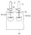
ケース3は、導電性の材料で形成されたもので、一端側に開口部3aを有し、他端側に底部3bを有した有底略円筒状のものである。このケース3の開口部3aには、気密端子4のリング12が圧入されており、これによってケース3は、その内部が真空状態で気密に封止されたものとなっている。
また、ケース3の底部3bには、外部へ突出する突起状の第二のアウターリード部(突起部)18が形成されている。このような構成のもとに本実施形態の圧電振動子1は、第一のアウターリード部16により、ケース3の外部からリード13を介して圧電振動片2の第一の励振電極8に導通可能であるとともに、第二のアウターリード部18により、ケース3の外部からケース3、リング12及びワイヤ17を介して圧電振動片2の第二の励振電極9に導通可能となっている。すなわち、ケース3に形成された第二のアウターリード部(突起部)18と前記した1本のリード13とを、一対の端子にしている。
The
Further, a projecting second outer lead portion (projection portion) 18 that protrudes to the outside is formed on the
なお、気密端子4のリング12においてステップ部12eのワイヤ17が接合する部分、及びインナーリード部15のバンプ接続部15aには、それぞれ部分的に金メッキ(図示せず)が施されており、これによって導通が良好になっている。このような金メッキとしては、ステップ部12e及びバンプ接続部15aにおいて、膜厚数千Å程度で成膜されている。
The portion of the
次に、この圧電振動子1の製造方法について説明する。
図4は本実施形態の圧電振動子1の製造工程のフロー図であり、図5から図26は、各製造工程の説明図である。本実施形態の圧電振動子1の製造工程は、圧電振動片を製造する圧電振動片製造工程S10と、気密端子4を製造する気密端子製造工程S20と、ケース3を製造するケース製造工程S30と、圧電振動片2、気密端子4、及びケース3を組立てる組立工程S40とに大きく分けられる。以下に、各工程を詳細に説明する。
Next, a method for manufacturing the
FIG. 4 is a flowchart of the manufacturing process of the
圧電振動片製造工程S10は、まず、水晶のランパード原石をスライスして所定の厚みのウエハを作製し、さらに、このウエハを一定の厚みになるまで研磨を行う。そして、このウエハに、フォトリソグラフィー技術によって水晶片2aの外形をパターニングしてエッチングすることで、ウエハから複数の水晶片2aを作製することができる。次に、作製された各水晶片2aについて、第一の励振電極8、第二の励振電極9、微調部10、粗調部11などとなる金属膜を成膜する。そして、各水晶片2aについて、粗調部11にレーザー光を照射して粗調部11を形成する金属膜の一部を蒸発させることで、重量を変化させ、これにより水晶片2aの共振周波数の粗調を行い、圧電振動片2が完成する。なお、水晶片2aの共振周波数をより高精度に調整する微調については、気密端子4に組み付けられた後に行う。そして、このようにして作製された複数の圧電振動片2は、図5に示すように、専用パレット30上に配列されて、後述する組立工程S40に搬送される。
In the piezoelectric vibrating reed manufacturing step S10, first, a quartz lampard ore is sliced to produce a wafer having a predetermined thickness, and the wafer is further polished to a certain thickness. A plurality of
次に、気密端子製造工程S20について説明する。気密端子製造工程S20は、まず、リング形成工程S21としてリング12の作製を行う。すなわち、図6(a)に示すように、リング12を形成する鉄ニッケルコバルト合金や鉄ニッケル合金などの導電性を有する板部材31にランス加工を施した後に、複数回深絞り加工を実施することで、リング12の圧入部12aの外径と略等しい有底の筒部材32が形成される。なお、筒部材32が形成される加工位置は、板部材31に予め形成された図示しないパイロット穴によって正確に位置決めされており、これによって複数の筒部材32を配列して形成することができる。
Next, the airtight terminal manufacturing process S20 will be described. In the airtight terminal manufacturing step S20, first, the
次に、図6(b)に示すようにサイジングを行い、縮径部12b及びステップ部12e、12fを形成する。すなわち、筒部材32の内、縮径部12bとなる部分についてさらに圧縮し、外径を縮径させるとともに、ステップ部12e、12fとなる部分については平面となるように型加工する。ここで、ステップ部12e、12fを中心軸L12に対して略対称に形成することで、縮径部12bを、全体に変形してしまうことなく均一な略円筒状に形成することができる。次に、図6(c)に示すように各筒部材32の底部32aを打ち抜き、天井穴32bを形成する。最後に、図6(d)に示すように、外形抜きを行うことで板部材31から筒部材32を離脱させ、リング12を完成させる。
Next, sizing is performed as shown in FIG. 6B to form the reduced
次に、リング12と、リード13と、充填部材14との組立を行う。すなわち、まずリング振込み工程S22として、図7に示すように、複数の凹部34を有するリング用カーボン冶具33に複数のリング12を装填していく。より詳しくは、リング用カーボン冶具33は、後述する充填部材焼成工程S25において充填部材14を焼成する際に使用可能にカーボンで形成されている。また、凹部34は、リング12を下向きに挿入可能に、底側にリング12の縮径部12bと対応する縮径部34a、及び、リング12のステップ部12e、12fと対応する平坦部34bが形成されている。複数の凹部34の各平坦部34bの向きは、相互に略等しくなるように形成されている。また、凹部34の底面からは、凹部34と同軸でリード13を挿入可能な挿入穴33aが形成されている。挿入穴33aの深さは、リード13のインナーリード部15の長さと対応しており、底版33bで閉塞されている。
Next, the
そして、このリング用カーボン冶具33の上面に複数のリング12を載置して、リング用カーボン冶具33に振動を与えることで、複数のリング12は、それぞれ、凹部34に向きを略等しくして装填されていくことになる。この際、リング12は、二つのステップ部12e、12fを中心軸L12に対して略対称として形成し、全体として略対称な部材として形成されていることで、振動により円滑に装填させていくことができる。
Then, by placing a plurality of
次に、充填部材振込み工程S23として、図8に示すように、リング用カーボン冶具33の凹部34に装填された各リング12の内部に、充填部材14を挿入していく。充填部材14は、後述する充填部材焼成工程S25によって焼成される前の形状につき、リング12の内部に挿入可能な外径を有するとともに、リード13を挿入可能な貫通孔14aを有した形状を呈している。そして、複数の充填部材14をリング用カーボン冶具33の上面に載置してリング用カーボン冶具33に振動を与えることで、各充填部材14は、リング12の内部に挿入されていくこととなる。
Next, as a filling member transfer step S23, as shown in FIG. 8, the filling
次に、リード振込み工程S24として、図9に示すように、各リング12の内部に挿入された充填部材14の貫通孔14aに、リード13を挿通させていく。まず、リング12及び充填部材14が装填されたリング用カーボン冶具33の上面に、リード用カーボン冶具35を載置する。リード用カーボン冶具35には、リード13を挿通可能な貫通孔35aが複数形成されている。また、リング用カーボン冶具33と、リード用カーボン冶具35とには、対応する図示しない位置決めピンと位置決め穴とが設けられていて、これにより互いに組み付けた状態で、凹部34と貫通孔35aとは同軸上に配置される。そして、複数のリード13をリード用カーボン冶具35の上面に載置してリング用カーボン冶具33及びリード用カーボン冶具35に振動を与えることで、各リード13は、リング12に挿入された充填部材14の貫通孔14aに挿通され、リング12の下方にインナーリード部15が、リング12の上方に第一のアウターリード部16が突出した状態で、リング12及び充填部材14と組み付けられる。
Next, as lead transfer process S24, as shown in FIG. 9, the
次に、充填部材焼成工程S25として、リング12及びリード13と組み付けられた状態で充填部材14の焼成を行う。すなわち、図11に示すように、リング12、リード13及び充填部材14が内部に装填された状態で、リング用カーボン冶具33及びリード用カーボン冶具35を加熱炉の内部に配置して所定の温度で加熱する。これにより、充填部材14は焼成されてリング12及びリード13のそれぞれとの間を気密に封止し、また、リング12、リード13及び充填部材14は一体となり、図11に示すように、気密端子4が形成される。なお、リード13のインナーリード部15のバンプ接続部15aは、後述するバンプ接続部形成工程S27で形成される。
Next, as the filling member firing step S25, the filling
次に、気密端子挿入工程S26として、気密端子4をリング用カーボン冶具33及びリード用カーボン冶具35から取り外し、ユニットフレーム36に配列させる。図12は気密端子4配列前のユニットフレーム36を、図13は気密端子4配列後のユニットフレーム36を示している。図12において省略しているが、ユニットフレーム36は帯状に連続する部材であり、長手方向に気密端子配置部37が等間隔に複数設けられている。気密端子配置部37は、各気密端子4においてリード13の第一のアウターリード部16を嵌合可能な一対の嵌合部37a、37bで構成されている。そして、図13に示すように、ユニットフレーム36の各気密端子配置部37に、上記工程で形成された各気密端子4を、リング12のステップ部12e、12fのいずれかが上方に向くようにして、第一のアウターリード部16を一対の嵌合部37a、37bに嵌合させて配置していく。ここで、気密端子4において、リング12のステップ部12e、12fは、中心軸L12に対して互いに略対称に形成されている。このため、ステップ部12e、12fのいずれを選択して上方に向くように配置したとしても、後述する第二のマウント工程S32で同じ条件でワイヤボンディングすることができる。すなわち、ステップ部を複数有していることで、上記の気密端子4の配置に際しては、後にワイヤボンディングする位置となるいずれかのステップ部を容易に上向きに調整することができる。
Next, in the airtight terminal insertion step S <b> 26, the
次に、バンプ接続部形成工程S27として、各気密端子4のインナーリード部15にバンプ接続部15aを形成する。すなわち、図14に示すように、ユニットフレーム36を移動させながら、順次ユニットフレーム36から突出する各気密端子4のインナーリード部15の先端部分を上方から押し潰していく。ここで、本実施形態のようにバンプ接続部形成工程S27を充填部材焼成工程S25後にすることで、上記のリード振込み工程S24及び充填部材焼成工程S25時にリング12のステップ部12e、12fとリード13のバンプ接続部15aとの相対的な向きを調整する必要が無い。また、バンプ接続部形成工程S27でバンプ接続部15aを形成する際には、リード13がリング12と一体化しているので、リング12のステップ部12e、12fとの相対的な向きを容易にかつ精度良く調整して、バンプ接続部15aを形成することができる。
Next, as a bump connection portion forming step S <b> 27,
次に、フレーム切断工程S28として、図15に示すように、帯状のユニットフレーム36を所定の長さ毎に裁断する。以下、裁断後のユニットフレームをパレット38と称す。
次に、メッキ工程S29として、図16に示すように、パレット38毎に、各気密端子4におけるリング12の圧入部12aの外周面及びステップ部12eの一部、並びに、リード13のバンプ接続部15aに金メッキを施す。
メッキは、下地メッキと仕上げメッキが施される。下地メッキには、例えば銅メッキが施される。リング12の圧入部12aの外周面の仕上げメッキには、ケース3との圧入嵌合で気密を保持するための例えば錫銅合金メッキが数μmから十μm程度の膜厚に施される。ステップ部12e及びバンプ接続部15aの仕上げメッキには金メッキが施される。
ステップ部12eにおける金メッキは、後述するワイヤボンディングを行うためのものであり、リード13のバンプ接続部15aにおける金メッキは、後述する圧電振動片2の第一の励振電極8とのバンプ接続のためのものである。ステップ部12e及びバンプ接続部15aの金メッキとしては、例えば数千Å程度の膜厚で形成される。
尚、ステップ部12e及びバンプ接続部15aは、錫銅合金メッキが施され、更にその上に金メッキが施されても良い。また、リング12の圧入部12aの錫銅合金メッキの表面にさらに金メッキが施されてもよい。
これにより、気密端子製造工程S20の全ての工程が完了する。
Next, as a frame cutting step S28, as shown in FIG. 15, the band-shaped
Next, as shown in FIG. 16, as the plating step S29, for each
For plating, base plating and finish plating are performed. For example, copper plating is applied to the base plating. In the finish plating of the outer peripheral surface of the press-fitting
The gold plating in the
Note that the
Thereby, all the steps of the hermetic terminal manufacturing step S20 are completed.
次に、ケース製造工程S30について説明する。このケース製造工程S30は、本発明におけるケースの製造方法の一実施形態となるものである。まず、板材準備工程S31として、ケース3の材料となる導電材料からなる板材を用意する。この板材としては、特にニッケルメッキ処理を施した洋白(洋銀)(C7521−R−O)が好適とされ、したがって本実施形態では、このようなニッケルメッキ処理を施した洋白を用いている。この板材については、まず幅が15mmの帯状の洋白(C7521−R−O)板を用意し、続いてその両面にニッケルメッキ処理を施して両面にそれぞれ1.2μm〜1.4μm程度の厚さのメッキ膜を形成する。そして、このようにして両面にメッキ膜を形成することにより、厚さ0.12mmの板材(フープ材)とする。また、このようにしてメッキ処理を施したら、これを巻回しさらにその長さ方向に沿って切断することにより、幅を6mmに調整する。これにより、以下の加工に供する板材を得る。
Next, the case manufacturing process S30 will be described. This case manufacturing process S30 is an embodiment of the method for manufacturing a case in the present invention. First, as a plate material preparation step S31, a plate material made of a conductive material as a material of the
このような帯状の板材を準備したら、ブランキング工程S32として、図17に示すようにこの板材70に対し、その円形の加工領域71の外側に、図示しないダイとパンチを用いて該加工領域71の周方向に沿って円弧状の貫通孔72を複数箇所(本例では4箇所)開ける。このように貫通孔72を形成し、板材70の非加工領域に対して加工領域71を部分的に分離しておくことで、後の深絞り工程を円滑に進めることが可能になる。
When such a strip-shaped plate material is prepared, as a blanking step S32, as shown in FIG. 17, the
次に、深絞り工程S33として、前記板材70の加工領域71に深絞り加工を行い、前記板材70を有底円筒状に加工する。本実施形態では、図18(a)〜(d)に示すように4次の深絞り加工を行い、板材70を段階的に深絞り加工することで有底円筒状に加工する。なお、この4次の深絞り加工では、各処理毎に寸法が異なる工具を用いることで、深絞りの度合いを段階的に高めている。また、図18(a)〜(d)では、左側(左図)に深絞り加工を行っている状態を示し、右側(右図)にこの深絞り加工で形成された板材70の形状を示している。
Next, as a deep drawing step S33, a deep drawing process is performed on the
図18(a)〜(d)の左図に示すように、この深絞り工程S33では、工具として凹部あるいは孔部を有するダイ73と、丸棒状のパンチ74とを用いている。これらダイ73とパンチ74とはモジュール化されており、図18(a)〜(d)で示す各処理、すなわち(a)の1次深絞り処理、(b)の2次深絞り処理、(c)の3次深絞り処理、(d)の4次深絞り処理において、それぞれ異なる寸法のダイ73とパンチ74とを用いる。
As shown in the left diagrams of FIGS. 18A to 18D, in the deep drawing step S33, a die 73 having a recess or a hole and a
ダイ73としては、本実施形態では開口形状が円形の凹部75を有したものが用いられ、これらダイ73は、(a)から(d)に進むにつれて凹部75の内径が段階的に小さくなっている。また、特に(c)の3次深絞り処理で用いられるダイ73では、凹部75の底面が凹面となるように形成されており、(d)の4次深絞り処理で用いられるダイ73では、凹部75の底面の中央部が(c)の場合よりも深い凹面となるように形成されている。
一方、パンチ74は円柱状のもので、その外径が、対応するダイ73の凹部75の内径より前記板材70の厚みにほぼ相当する分小さくなっている。なお、これらパンチ74は、その下端面の周縁部が丸め加工されてRが付与されており、これによってその周縁部で板材70を損傷しないようになっている。また、特に(c)の3次深絞り処理で用いられるパンチ74、および(d)の4次深絞り処理で用いられるパンチ74では、その下端面が対応するダイ73の凹部75の底面形状に対応して、凸面に形成されている。
In this embodiment, the dies 73 having
On the other hand, the
このようなダイ73とパンチ74とを用いて深絞り加工を行うには、まず、前記ブランキング工程S32後の帯状の板材70をダイ73上に載せ、その加工領域71をダイ73の凹部75に位置合わせする。続いて、図18(a)の左図に示すように板材70の上からパンチ74を降下させ、前記凹部75内に圧入する。これにより、板材70はその加工領域71が1次深絞り処理され、図18(a)中の右図に示すように外径が比較的大きく、かつ深さが比較的浅い有底円筒状となる。次いで、パンチ74を上昇させることで板材70を共に引き上げる。その後、板材70をパンチ74から脱離させ、これを移送することで次の工具に移動する。
In order to perform deep drawing using such a
すなわち、加工領域71を次のダイ73上に載せ、以下、前記した1次深絞り処理と同様にして、図18(b)に示すように2次深絞り処理を行い、さらに図18(c)に示す3次深絞り処理、図18(d)に示す4次深絞り処理を順次行う。なお、板材70は帯状に長く連続しているので、図18(b)に示す2次深絞り処理を行っている加工領域71に隣合う加工領域71は、図18(a)に示した1次深絞り処理が施されることになる。また、加工領域71が3次深絞り処理、4次深絞り処理と進むに連れ、後続する加工領域71も順次処理が進むようになる。ここで、各加工領域71は、板材70に予め形成された図示しないパイロット穴によって正確に位置決めされており、これによって複数の加工領域71が順次移送され、連続的に絞り処理されるようになっている。
That is, the
また、特に図18(c)に示す3次深絞り処理を行った後には、図18(c)中の右図に示すように板材70は、その底部が外側に略球面状に膨出した形状となり、さらに図18(d)に示す4次深絞り処理を行った後には、図18(d)中の右図に示すように板材70は、その底部の中心部が外周部に対して突出した形状となる。また、これら3次深絞り処理、4次深絞り処理では、有底円筒状に加工された加工領域71は、ダイ73の凹部75内に全てが入り込まず、開口部側がダイ73の上方に浮いた状態で加工されるようになっている。
In particular, after the third deep drawing process shown in FIG. 18 (c), the bottom of the
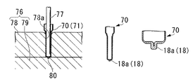
このようにして1次から4次の絞り処理による深絞り工程S33を行い、図18(d)中の右図に示すように板材70を有底円筒状に加工したら、この板材70を、続いて段絞り工程S34に進ませる。
この段絞り工程S34は、基本的には前記の深絞り工程S33と同様に、ダイ76とこれに対応するパンチ77とからなる工具を用いて絞り加工を段階的に高めていくものである。すなわち、この段絞り工程S34は、本実施形態では、図19(a)〜(d)に示すように4次の段絞り加工を行い、板材70を段階的に段絞り加工することで、先に有底円筒状に加工された板材の底部の外面に、前記した第2のアウターロード部18となる突起部を形成する。
When the deep drawing step S33 by the first to fourth drawing processes is performed in this way and the
In this step drawing step S34, the drawing process is basically enhanced stepwise using a tool comprising a
この4次の段絞り加工でも、各処理毎に寸法が異なる工具を用いることで、段絞りの度合いを段階的に高めている。なお、図19(a)〜(d)、および後述する図20では、左側(左図)に段絞り加工を行っている状態を示し、中央部(中央図)この段絞り加工で形成された板材70の形状を示し、右側(右図)に段絞り加工で形成された板材70の底部の形状を拡大して示している。
図19(a)〜(d)の左図に示すように、この段絞り工程S34では、工具として凹部あるいは孔部を有するダイ76と、棒状のパンチ77とを用いている。これらダイ73とパンチ74とはモジュール化されており、図19(a)〜(d)で示す各処理、すなわち(a)の1次段絞り処理、(b)の2次段絞り処理、(c)の3次段絞り処理、(d)の4次段絞り処理において、それぞれ異なる寸法のダイ76とパンチ77とを用いる。
Even in this fourth-order step drawing, the degree of step drawing is increased stepwise by using tools having different dimensions for each process. In FIGS. 19A to 19D and FIG. 20 described later, the left side (left figure) shows a state in which step drawing is performed, and the center part (center figure) is formed by this step drawing. The shape of the
19A to 19D, in the step drawing step S34, a die 76 having a recess or a hole and a rod-shaped
ダイ76としては、本実施形態では開口形状が円形の貫通孔78aを有した上ダイ78と、同じく開口形状が円形の孔部79aを有した下ダイ79とからなるものが用いられる。これら上ダイ78と下ダイ79とは、それぞれの貫通孔78aと孔部79aとが連通させられ、かつ、これら貫通孔78aと孔部79aとの中心軸が一致させられた状態で接合され、用いられる。ここで、下ダイ79の孔部79aは、特に下ダイ79の上面側とその下方とが異なる径に形成されているが、本実施形態において段絞り加工に直接用いられる部分は、下ダイ79の上面側のみであるので、孔部79aと記したときには下ダイ79の上面側の孔部を指すものとする。このような構成からなる下ダイ79は、(a)から(d)に進むにつれて、孔部79a(下ダイ79上面側の孔)の内径が段階的に小さくなっている。一方、上ダイ78については、その貫通孔78aは(a)から(d)において同一になっている。
In this embodiment, the
また、(a)〜(d)の各段絞り処理で用いられる下ダイ79では、その孔部79aにおける下ダイ79上面側の開口部が、開口側から下側に行くに連れて縮径されており、その後、一定の内径に形成されている。ここで、この一定の内径に形成されている部分を、本発明では、「深絞り工程で略有底円筒状に加工された板材の底部の外径より小さい内径の凹部あるいは孔」としている。
In addition, in the
一方、これらダイ73に対応するパンチ77は、深絞り加工でのものと同様に円柱状のもので、その外径が、対応する上ダイ78の貫通孔78aの内径より前記板材70の厚みにほぼ相当する分小さくなっている。なお、これらパンチ77にあっても、その下端面の周縁部が丸め加工されてRが付与されており、これによってその周縁部で板材70を損傷しないようになっている。そして、これらパンチ78は、その下端面に、対応する下ダイ79の開口部の形状に対応して、その中央部に突出部が形成されている。これらパンチ78の突出部は、(a)〜(d)に進むに連れてその外径や高さが小さくなっている。
On the other hand, the
このようなダイ76とパンチ77とを用いて段絞り加工を行うには、まず、前記深絞り加工後の有底円筒状の板材70を、図19(a)中の左図に示したダイ76の上ダイ78上に載せ、その有底円筒部分の底部側を上ダイ78の貫通孔78aに位置合わせする。続いて、図19(a)中の左図に示すように板材70の上からパンチ77を降下させ、前記貫通孔78a内に圧入する。これにより、有底円筒状の板材70はその円筒部分が貫通孔78a内に入り込み、さらにその底部が下ダイ79の孔部79a内に入り込む。このようにしてパンチ77を圧入すると、有底円筒状の板材70はその底部が、下ダイ79の孔部79aの開口部内、すなわち該孔部79における一定の内径に形成された部分の開口部を含む面に当接させられ、板材70の底部は、図19(a)中の右図に示すようにこの面に対応した形状に1次段絞りされる。
In order to perform step drawing using such a
次いで、パンチ77を上昇させることで板材70を共に引き上げる。その後、板材70をパンチ77から脱離させ、これを移送することで次の工具に移動する。
すなわち、有底円筒状の板材70を次のダイ76上に載せ、以下、前記した1次段絞り処理と同様にして、図19(b)に示すように2次段絞り処理を行い、さらに図19(c)に示す3次段絞り処理、図19(d)に示す4次段絞り処理を順次行う。なお、板材70は帯状に長く連続しているので、有底円筒状の被加工部分が各工具に順次移送され、連続的に段絞り処理されるのは、前記の深絞り工程の場合と同様である。
Next, the
That is, the bottomed
このようにして1次から4次の段絞り処理による段絞り工程S34を行うことにより、図19(d)中の右図に示すように、有底円筒状の板材70の底部に突起部18aを形成する。ただし、本実施形態では、この突起部18aは図1に示した第2のアウターリード部18より長く形成され、かつその外径が小さく(細く)形成されている。そこで、このように所望の長さより長い突起部18aを形成したら、この有底円筒状の板材70を、続いて調整工程S35に進ませる。
In this way, by performing the step drawing step S34 by the first to fourth step drawing processing, as shown in the right diagram in FIG. 19D, the
この調整工程S35は、前記の段絞り工程S34と同様に、ダイ76とこれに対応するパンチ77とからなる工具を用いてサイジング加工を行うものである。すなわち、この調整工程S35は、本実施形態では、図20に示すように開口形状が円形の貫通孔78aを有した上ダイ78と、同じく開口形状が円形の穴部80を有した下ダイ79とからなるものを用い、前記突起部18aを圧縮することにより、該突起部18aを所望の長さに調整する。ここで、前記穴部80は、図1に示した第2のアウターリード部18の長さ、つまり所望の長さに対応する所望の深さを有し、かつ、第2のアウターリード部18の太さ、つまり所望の外径に対応する所定の内径を有するものである。
In the adjustment step S35, as in the step drawing step S34, sizing is performed using a tool including a
このようなサイジング加工を行うには、まず、前記段絞り加工後の有底円筒状の板材70をダイ76の上ダイ78上に載せ、その有底円筒部分の底部側を上ダイ78の貫通孔78aに位置合わせする。続いて、図20中の左図に示すように板材70の上からパンチ77を降下させ、前記貫通孔78a内に圧入する。これにより、有底円筒状の板材70はその円筒部分が貫通孔78a内に入り込み、さらにその底部の突起部18aが下ダイ79の穴部80内に入り込む。このようにしてパンチ77を所定時間圧入すると、前記突起部18aは前記の穴部80に圧入され、これにより突起部18aを形成している底部は貫通孔78a内において下ダイ79の上面に当接した状態で押圧される。したがって、前記突起部18aはその先端側が下ダイ79の穴部80の底面に相対的に押圧され、板材70の底部側がパンチ77で押圧されることにより、その長さが穴部80の深さと対応する長さに圧縮され、かつ、肉寄せされることでその太さ(外径)が穴部80の内径と対応する太さ(外径)に調整される。これにより、前記の突起部18aはその長さと太さ(外径)が、図1に示した第2のアウターリード部18と同じに調整される。
In order to perform such sizing processing, first, the bottomed
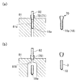
このようにして突起部18aの調整を行ったら、この突起部を形成した略有底円筒状の板材70を、その開口部側の所定の位置で切断する切断工程S36に進ませる。
この切断工程S36は、前記の深絞り工程S33と同様に、ダイ81とこれに対応するパンチ82とからなる工具を用いて行うもので、本実施形態では、プレカット加工とトリミング加工とをこの順に行うものである。
After adjusting the
This cutting step S36 is performed using a tool including a
プレカット加工では、図21(a)中の左図に示すように開口形状が円形の貫通孔81aを有したダイ81を用い、この貫通孔81a内に前記板材70の突起部18a側を入れる。そして、その状態でパンチ82を有底円筒状の板材70内に圧入し、切断部分を薄肉化する。
次いで、トリミング工程では、図21(b)中の左図に示すように開口形状が円形の貫通孔81bを有したダイ81を用い、この貫通孔81b内に、プレカット加工後の板材70の突起部18a側を入れる。そして、その状態でパンチ82を有底円筒状の板材70内に圧入する。ここで、このトリミング工程で用いるパンチ82としては、その周縁部が切刃になっているものを用いる。したがって、このパンチ82を板材70内に圧入することにより、予め設定された切断位置で切断することができる。これにより、図21(b)中の右図に示すように、所定の寸法の突起部(第2のアウターリード部18)を一体に形成してなるケース3が得られる。このようにして得られたケース3は、その筒状部における厚さ(板厚)が、約0.05mmとなっていた。また、その表面に施されたメッキは、剥離することなくそのままメッキ膜の状態で残っていた。
In the pre-cut processing, as shown in the left diagram in FIG. 21A, a die 81 having a through
Next, in the trimming process, as shown in the left diagram of FIG. 21B, a die 81 having a through
なお、このようなケース製造工程S30では、特に板材準備工程S31において帯状に長く連続した板材70を用意しているので、その後のブランキング工程S32、深絞り工程S33、段絞り工程S34、調整工程S35、切断工程S36では、板材70の加工領域71を各処理に対応する各工具に順次移送することにより、これら処理を連続的に行うことができる。したがって、処理の自動化、高効率化(高速化)が可能になっている。
In this case manufacturing process S30, the
次に、組立工程S40として、前記の各工程で得られた圧電振動片2、ケース3、及び、気密端子4の組立を行う。まず、第一のマウント工程S31として、図22に示すように、パレット38において、各気密端子4のインナーリード部15に圧電振動片2を搭載する。すなわち、圧電振動片製造工程S10で作製された圧電振動片2を専用パレット30上から取り出す。そして、各気密端子4のインナーリード部15において金メッキが施されたバンプ接続部15aに、取り出した圧電振動片2の第一の励振電極8を基部7でバンプ接続させる。バンプ接続の条件としては、例えば、実装温度130℃、ボンド荷重0.5N、荷重時間が15×10−3秒程度である。これにより、圧電振動片2の第一の励振電極とリード13とは電気的に接続された状態となるとともに、圧電振動片2は、リード13のインナーリード部15に片持ち状に支持された状態となる。ここで、リード13のインナーリード部15において圧電振動片2をバンプ接続する部分が、バンプ接続部15aとして略平面に形成されていることで、より確実に、第一の励振電極8とリード13との導通を図ることができるとともに、リード13によって圧電振動片2を支持することができる。また、バンプ接続部15aがリード13の中心軸と略等しい位置まで押し潰して形成されていることで、圧電振動片2をリード13の中心軸に略等しい位置でリード13と接合することができる。
Next, as an assembly step S40, the piezoelectric vibrating
次に、第二のマウント工程S32として、図23に示すように、各気密端子4のリング12のステップ部12e、12fから選択されたステップ部12eと、各気密端子4に搭載された圧電振動片2の第二の励振電極9とをワイヤボンディングする。本実施形態においては、ステップ部12eと第二の励振電極9との間に2本のワイヤ17をボンディングしている。使用されるワイヤ17としては、例えば金(Au)線が選択され、このワイヤ17の一端を、圧電振動片2の基部7において第二の励振電極9にボンディングした後に、他端を、リング12のステップ部12eにボンディングする。ワイヤボンディングの各条件としては、例えば、実装温度130℃、ワイヤ径25μm、ボール径80〜85μm、ボール厚13μm、せん断強度0.45〜0.53Nであり、第二の励振電極9にボンディングする際のボンド荷重が0.55N、荷重時間が7×10⁻³秒、ステップ部12eにボンディングする際のボンド荷重が0.4N、荷重時間が5×10⁻³秒程度である。これにより、圧電振動片2の第二の励振電極9とリング12とは電気的に接続された状態となる。ここで、縮径部12bの外周面の内、略平面に形成されたステップ部12eにボンディングすることで、確実に導通を図ることができる。特に、複数のワイヤ17によって接続することで、より確実に導通を図ることができる。なお、第一の励振電極8と接続されたリード13と、第二の励振電極9と接続されたリング12とは、その間に絶縁性の充填部材14が介装されていることで絶縁された状態であり、これにより圧電振動片2の第一の励振電極8と第二の励振電極9とを絶縁した状態とし、短絡を防ぐことができる。
Next, as a second mounting step S32, as shown in FIG. 23, the
次に、微調工程S33として、圧電振動片2の微調を行う。すなわち、図24に示すように、真空雰囲気中において、リング12の圧入部12aの外周面及びパレット38に設定したコンタクト39に電極を接触させて電圧を印加することで、圧電振動片2の振動腕部5、6を振動させる。そして、微調部10にレーザー光を照射して微調部10を形成する金属膜を蒸発させながら振動腕部5、6の周波数を測定することで、圧電振動片2の振動腕部5、6の振動が所定の共振周波数となるように微調整を行う。
Next, as a fine adjustment step S33, fine adjustment of the piezoelectric vibrating
次に、圧入工程S44として、図25に示すように真空雰囲気中において、前記のケース製造工程S30で所定形状に形成したケース3に、その開口部3a側から各圧電振動片2を挿入し、さらにこのケース3に気密端子4のリング12を圧入する。これにより、圧電振動片2は、ケース3の内部に気密に封止された状態となる。最後に切り離し工程S45として、図26に示すように、リード13の第一のアウターリード部16の内、パレット38の気密端子配置部37に嵌合されている部分を切り離すことで、圧電振動子1が完成する。
Next, as the press-fitting step S44, in a vacuum atmosphere as shown in FIG. 25, each piezoelectric vibrating
以上のように、本実施形態の圧電振動子1では、ケース3の内部に配設された圧電振動片2の第一の励振電極8及び第二の励振電極9について、第一の励振電極8はリード13の第一のアウターリード部16によって、また、第二の励振電極9はケース3の第二のアウターリード部18によってリング12及びケース3を介して、それぞれ互いに短絡してしまうことなく外部から導通を図ることができる。ここで、第二の励振電極9と縮径部12bに形成されたステップ部12eとは、ケース3の内周面とリング12のステップ部12eとの間に形成される隙間12dを利用してワイヤ17を配設して接続することができ、ケース3及びリング12の外径が大きくなってしまうことが無い。また、リング12は、圧入部12aと、縮径部12bと、ステップ部12e、12fとを有する単純な構造であるので、外径を小さくしてもプレス加工によって容易に形成することができる。このため、本実施形態の圧電振動子1では、短絡を防止しつつ小型化を図るとともに、容易に歩留まり良く製造することが可能である。また、圧電振動片2は、略平面に形成されたバンプ接続部15aによってリード13の中心軸と略等しい位置に配置されることで、リード13とともにケース3の中心軸L3に略等しい位置に配置することができる。このため、ケース3の内周面と圧電振動片2との離隔を圧電振動片2が変位する範囲に応じて最小限の大きさに設定することができ、それ故にケース3及びリング12の小型化をさらに図ることができる。
As described above, in the
また、ケース3が、深絞り工程や段絞り工程を経ることで第二のアウターリード部18(突起部)を一体に形成しているので、従来のようなはんだ付けを行う工程が不要になっている。したがって、このケース3の製造が容易になっていることから、このケース3を備えてなる圧電振動子1自体も、その製造の容易化が図られたものとなっている。
なお、前記実施形態では、特にケース製造工程S30において、段絞り工程S34の後に調整工程S35を経ることにより、形成する突起部18a(第二のアウターリード部18)の長さを調整したが、段絞り工程S34で得られる突起部18aの長さや太さ(外径)を所望の寸法に形成できれば、調整工程S35を省略することもできる。
In addition, since the
In the embodiment, the length of the
(第2の実施形態)
図27及び図28は、この発明に係る第2の実施形態を示している。この実施形態において、前述した実施形態で用いた部材と共通の部材には同一の符号を付して、その説明を省略する。
(Second Embodiment)
27 and 28 show a second embodiment according to the present invention. In this embodiment, members that are the same as those used in the above-described embodiment are assigned the same reference numerals, and descriptions thereof are omitted.
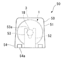
図27及び図28に示すように、この実施形態の圧電振動子50は、第1の実施形態の圧電振動子1を樹脂モールドした表面実装型の圧電振動子である。より詳しくは、圧電振動子50は、ケース3と、ケース3の開口部3aを気密に封止する気密端子4と、ケース3の内部に配設された図示しない圧電振動片2と、樹脂で形成され、ケース3、第一のアウターリード部16及び第二のアウターリード部18を覆う樹脂体51とを備える。第一のアウターリード部16及び第二のアウターリード部18には、それぞれ外部端子52が接続されている。外部端子52は、第一のアウターリード部16または第二のアウターリード部18に嵌合されるV字状の溝53aを有する嵌合部53と、嵌合部53の下端に設けられて、一面54aが樹脂体51の外側に露出する外部接続部54とを有する。
As shown in FIGS. 27 and 28, the
このような圧電振動子50においても、圧電振動子の両面に設けられた図示しない励振電極同士が短絡してしまうこと無く、小型化を図ることができるとともに、容易に製造することができ、例えば樹脂体51の外形形状として、断面が一辺1.1mm以下で、長さが4.3mm以下の圧電振動子を実現することができる。このため、より小さいスペースで基板上に搭載することができ、基板上の省スペース化を図ることができる。
Such a
(第3の実施形態)
図29は、この発明に係る第3の実施形態を示している。この実施形態において、前述した実施形態で用いた部材と共通の部材には同一の符号を付して、その説明を省略する。
図29は、本発明に係る音叉型水晶発振器の構成を示す概略図であり、上述した圧電振動子を利用した表面実装型圧電発振器の平面図を示している。図29に示すように、この実施形態の発振器100は、シリンダーパッケージ型の圧電振動子1を、集積回路101に電気的に接続された発振子として構成したものである。なお、圧電振動子1については、第1の実施形態のものと同様であるので、その説明を省略する。この発振器100は、コンデンサ等の電子部品102が実装された基板103を備えている。基板103には、発振器用の集積回路101が実装されていて、この集積回路101の近傍に、圧電振動子1が実装されている。これら電子部品102、集積回路101及び圧電振動子1は、図示しない配線パターンによってそれぞれ電気的に接続されている。なお、各構成部品は、図示しない樹脂によりモールドされている。
(Third embodiment)
FIG. 29 shows a third embodiment according to the present invention. In this embodiment, members that are the same as those used in the above-described embodiment are assigned the same reference numerals, and descriptions thereof are omitted.
FIG. 29 is a schematic diagram showing a configuration of a tuning fork type crystal oscillator according to the present invention, and shows a plan view of a surface mount type piezoelectric oscillator using the above-described piezoelectric vibrator. As shown in FIG. 29, the
このように構成された発振器100において、圧電振動子1に電圧を印加すると、圧電振動子1内の圧電振動片2が振動し、この振動が水晶の圧電特性により電気信号に変換されて、集積回路101に電気信号として入力される。入力された電気信号は、集積回路101によって各種処理がなされ、周波数信号として出力される。これにより、圧電振動子1が発振子として機能する。また、集積回路101の構成を、例えば、RTC(リアルタイムクロック)モジュール等を要求に応じて選択的に設定することで、時計用単機能発振器等の他、当該機器や外部機器の動作日や時刻を制御したり、時刻やカレンダー等を提供したりする機能を付加することができる。
In the
以上のように、本実施形態の発振器100によれば、上記のような小型で、かつ、短絡のおそれが無い圧電振動子1を備えることで、小型で、信頼性の高い発振器を提供することができる。
なお、上記の発振器100は、シリンダーパッケージタイプの圧電振動子1を備えるものとして説明したが、これに限るものでは無く、例えば、第2の実施形態で示した表面実装型パッケージタイプの圧電振動子50としても良い。
As described above, according to the
The
(第4の実施形態)
図30は、この発明に係る第4の実施形態を示している。この実施形態において、前述した実施形態で用いた部材と共通の部材には同一の符号を付して、その説明を省略する。
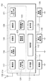
この実施形態においては、電子機器として、上述した圧電振動子1を有する携帯情報機器を例にして説明する。図30は、この電子機器の構成を示すブロック図である。図30に示すように、この実施形態の携帯情報機器110は、圧電振動子1と、電力を供給するための電源部111とを備えている。電源部111は、例えば、リチウム二次電池で構成されている。この電源部111には、各種制御を行う制御部112と、時刻等のカウントを行う計時部113と、外部との通信を行う通信部114と、各種情報を表示する表示部115と、それぞれの機能部の電圧を検出する電圧検出部116とが並列に接続されている。そして、電源部111によって、各機能部に電力が供給されるようになっている。
(Fourth embodiment)
FIG. 30 shows a fourth embodiment according to the present invention. In this embodiment, members that are the same as those used in the above-described embodiment are assigned the same reference numerals, and descriptions thereof are omitted.
In this embodiment, a portable information device having the above-described
制御部112は、各機能部を制御して音声データの送信及び受信、現在時刻の計測や表示等、システム全体の動作制御を行う。また、制御部112は、予めプログラムが書き込まれたROMと、ROMに書き込まれたプログラムを読み出して実行するCPUと、CPUのワークエリアとして使用されるRAM等とを備えている。
The
計時部113は、発振回路、レジスタ回路、カウンタ回路及びインターフェース回路等を内蔵する集積回路と、圧電振動子1とを備えている。圧電振動子1に電圧を印加すると圧電振動片2が振動し、この振動が水晶の有する圧電特性により電気信号に変換されて、発振回路に電気信号として入力される。発振回路の出力は二値化され、レジスタ回路とカウンタ回路とにより計数される。そして、インターフェース回路を介して、制御部112と信号の送受信が行われ、表示部115に、現在時刻や現在日付或いはカレンダー情報等が表示される。
The
通信部114は、従来の携帯電話と同様の機能を有し、無線部117、音声処理部118、切替部119、増幅部120、音声入出力部121、電話番号入力部122、着信音発生部123及び呼制御メモリ部124を備えている。無線部117は、音声データ等の各種データを、アンテナ125を介して基地局と送受信のやりとりを行う。音声処理部118は、無線部117又は増幅部120から入力された音声信号を符号化及び複号化する。増幅部120は、音声処理部118又は音声入出力部121から入力された信号を、所定のレベルまで増幅する。音声入出力部121は、スピーカやマイクロフォン等から構成され、着信音や受話音声を拡声したり、音声を集音したりする。
The
また、着信音発生部123は、基地局からの呼び出しに応じて着信音を生成する。切替部119は、着信時に限って、音声処理部118に接続されている増幅部120を着信音発生部123に切り替えることによって、着信音発生部123において生成された着信音が増幅部120を介して音声入出力部121に出力される。なお、呼制御メモリ部124は、通信の発着呼制御に係るプログラムを格納する。また、電話番号入力部122は、例えば、0から9の番号キー及びその他のキーを備えていて、これら番号キー等を押下することにより、通話先の電話番号等が入力される。
In addition, the
電圧検出部116は、電源部111によって制御部112等の各機能部に対して加えられている電圧が、所定の値を下回った場合に、その電圧降下を検出して制御部112に通知する。このときの所定の電圧値は、通信部114を安定して動作させるために必要な最低限の電圧として予め設定されている値であり、例えば、3V程度となる。電圧検出部116から電圧降下の通知を受けた制御部112は、無線部117、音声処理部118、切替部119及び着信音発生部123の動作を禁止する。特に、消費電力の大きな無線部117の動作停止は、必須となる。更に、表示部115に、通信部114が電池残量の不足により使用不能になった旨が表示される。
When the voltage applied to each functional unit such as the
すなわち、電圧検出部116と制御部112とによって、通信部114の動作を禁止し、その旨を表示部115に表示することができる。この表示は、文字メッセージであっても良いが、より直感的な表示として、表示部115の表示面の上部に表示された電話アイコンに、×(バツ)印を付けるようにしても良い。なお、携帯情報機器110は、通信部114の機能に係る部分の電源を、選択的に遮断することができる電源遮断部126を備えており、この電源遮断部126によって、通信部114の機能が確実に停止される。
That is, the operation of the
この実施形態の携帯情報機器110によれば、上記のような小型で、かつ、短絡のおそれが無い圧電振動子1を備えることで、小型で、信頼性の高い携帯情報機器を提供することができる。
なお、上記の携帯情報機器110は、シリンダーパッケージタイプの圧電振動子1を備えるものとして説明したが、これに限るものでは無く、例えば第2の実施形態に示す表面実装型パッケージタイプの圧電振動子50としても良い。圧電振動子50を実装するものとすれば、他の電子部品と同時にプリント基板上にリフロー半田にて接続できるためより好適である。
According to the portable information device 110 of this embodiment, it is possible to provide a portable information device that is small and highly reliable by including the
The portable information device 110 has been described as including the cylinder package type
(第5の実施形態)
図30は、この発明に係る第5の実施形態を示している。この実施形態において、前述した実施形態で用いた部材と共通の部材には同一の符号を付して、その説明を省略する。
この実施形態においては、電波時計の一実施形態として、上述した圧電振動子1を有する電波時計について説明する。図30は、この電波時計の構成を示すブロック図である。図30に示すように、この実施形態の電波時計130は、フィルタ部131に電気的に接続された圧電振動子1を備えたものであり、時計情報を含む標準の電波を受信して、正確な時刻に自動修正して表示する機能を備えた時計である。日本国内には、福島県(40kHz)と佐賀県(60kHz)とに、標準の電波を送信する送信所(送信局)があり、それぞれ標準電波を送信している。40kHz若しくは60kHzのような長波は、地表を伝播する性質と、電離層と地表とを反射しながら伝播する性質とを併せもつため、伝播範囲が広く、上述した2つの送信所で日本国内を全て網羅している。
(Fifth embodiment)
FIG. 30 shows a fifth embodiment according to the present invention. In this embodiment, members that are the same as those used in the above-described embodiment are assigned the same reference numerals, and descriptions thereof are omitted.
In this embodiment, a radio timepiece having the above-described
アンテナ132は、40kHz若しくは60kHzの長波の標準電波を受信する。長波の標準電波は、タイムコードと呼ばれる時刻情報を、40kHz若しくは60kHzの搬送波にAM変調をかけたものである。受信された長波の標準電波は、アンプ133によって増幅され、複数の圧電振動子1を有するフィルタ部131によって濾波、同調される。
なお、圧電振動子1として、上記搬送周波数と同一の40kHz及び60kHzの共振周波数を有する圧電振動子部134、135をそれぞれ備えている。
The
The
さらに、濾波された所定周波数の信号は、検波、整流回路136により検波復調される。そして、波形整形回路137を介してタイムコードが取り出され、CPU138でカウントされる。CPU138では、現在の年、積算日、曜日、時刻等の情報を読み取る。読み取られた情報は、RTC139に反映され、正確な時刻情報が表示される。搬送波は40kHz若しくは60kHzであるから、圧電振動子部134、135は、上述した音叉型の構造を持つ圧電振動子が好適である。60kHzを例にとれば、音叉型振動子片の寸法例として、全長が約2.8mm、基部の幅寸法が約0.5mmの寸法で構成することが可能である。
Further, the filtered signal having a predetermined frequency is detected and demodulated by the detection and
この実施形態の電波時計130によれば、上記のような小型で、かつ、短絡のおそれが無い圧電振動子1を備えることで、小型で、信頼性の高い電波時計を提供することができる。
なお、上記の電波時計130は、シリンダーパッケージタイプの圧電振動子1を備えるものとして説明したが、これに限るものでは無く、例えば第2の実施形態に示す表面実装型パッケージタイプの圧電振動子50としても良い。
According to the radio-controlled
Although the above-described
以上、本発明の実施形態について図面を参照して詳述したが、振動のモードは、音叉型である屈曲振動に限定されず、厚み滑り振動モード等の他の振動モードの振動片であっても良い。また、圧電体材料は、水晶に限定されず、ニオブ酸リチウム、タンタル酸リチウム、ランガサイト等の圧電材料であっても良い。また、具体的な構成はこの実施形態に限られるものではなく、本発明の要旨を逸脱しない範囲の設計変更等も含まれる。 As described above, the embodiment of the present invention has been described in detail with reference to the drawings. However, the vibration mode is not limited to the bending vibration that is a tuning fork type, and is a vibration piece of another vibration mode such as a thickness-shear vibration mode. Also good. Further, the piezoelectric material is not limited to quartz, and may be a piezoelectric material such as lithium niobate, lithium tantalate, or langasite. Further, the specific configuration is not limited to this embodiment, and includes design changes and the like within a range not departing from the gist of the present invention.
1、50 圧電振動子 2 圧電振動片 3 ケース 3a 開口部 8 第一の励振電極(励振電極) 9 第二の励振電極(励振電極) 12 リング 12a 圧入部 12b 縮径部 12c 外周面 12d 隙間 12e、12f ステップ部 13 リード 14 充填部材 14a 貫通孔 15 インナーリード部 15a ボンド接続部 16 第一のアウターリード部(アウターリード部) 17 ワイヤ 18 第二一のアウターリード部(突起部) 18a 突起部 51 パッケージ 70 板材 71 加工領域 76 ダイ 77 パンチ 79 下ダイ 79a 孔部(孔) 80 穴部 100 発振器 110 携帯情報機器(電子機器) 130 電波時計 L3 中心軸 S30 ケース製造工程 S33 深絞り工程 S34 段絞り工程 S35 調整工程 S36 切断工程
DESCRIPTION OF
Claims (10)
導電材料からなる板材に深絞り加工を行い、前記板材を略有底円筒状に加工する深絞り工程と、
前記深絞り工程で略有底円筒状に加工された板材の底部の外面を、該底部の外径より小さい内径の凹部あるいは孔を有するダイの、前記凹部あるいは孔の開口部を含む面に当接させつつ、該板材の底部の内面をパンチで押圧して段絞り加工を行うことにより、該底部の外面に突起部を形成する段絞り工程と、
前記段絞り工程で突起部を形成した略有底円筒状の板材を、その開口部側の所定の位置で切断することにより、突起部を有する略有底円筒状のケースを得る切断工程と、を備えたことを特徴とするケースの製造方法。 A method of manufacturing a case for housing the piezoelectric vibrating piece in a piezoelectric vibrator comprising the piezoelectric vibrating piece,
Deep drawing process is performed on a plate material made of a conductive material, and the plate material is processed into a substantially bottomed cylindrical shape,
The outer surface of the bottom of the plate material processed into a substantially bottomed cylindrical shape in the deep drawing step is contacted with the surface including the recess or hole opening of the die having an inner diameter smaller than the outer diameter of the bottom. A step drawing step of forming a projection on the outer surface of the bottom by pressing the inner surface of the bottom of the plate with a punch while making contact,
A cutting step of obtaining a substantially bottomed cylindrical case having a protruding portion by cutting the substantially bottomed cylindrical plate material having the protruding portion formed in the step-drawing step at a predetermined position on the opening side thereof; A method for manufacturing a case, comprising:
前記段絞り工程では、前記突起部の長さを所望の長さより長くなるように形成し、
前記段絞り工程の後に、前記突起部の長さを所望の長さに調整する調整工程を有していることを特徴とするケースの製造方法。 In the manufacturing method of the case according to claim 1,
In the step-drawing step, the length of the protrusion is formed to be longer than a desired length,
A method for manufacturing a case, comprising: an adjusting step of adjusting a length of the protruding portion to a desired length after the step drawing step.
前記調整工程では、前記所望の長さに対応する所望の深さで所定の内径を有する穴部を有したダイを用い、前記の所望の長さより長い突起部を前記穴部に挿入し、その状態で前記板材の底部の内面をパンチで押圧することにより、前記突起部を所望の長さに圧縮することを特徴とするケースの製造方法。 In the manufacturing method of the case according to claim 2,
In the adjusting step, using a die having a hole having a predetermined inner diameter at a desired depth corresponding to the desired length, a protrusion longer than the desired length is inserted into the hole, A method of manufacturing a case, wherein the protrusion is compressed to a desired length by pressing the inner surface of the bottom of the plate with a punch in a state.
前記板材は複数個のケースを形成するための連続した帯状のものであることを特徴とするケースの製造方法。 In the manufacturing method of the case as described in any one of Claim 1 to 3,
The method of manufacturing a case, wherein the plate material is a continuous belt-shaped member for forming a plurality of cases.
前記板材はメッキ処理後のものであることを特徴とするケースの製造方法。 In the manufacturing method of the case according to any one of claims 1 to 4,
The method of manufacturing a case, wherein the plate material is after plating.
前記板材は厚さが0.12mmのものであることを特徴とするケースの製造方法。 In the manufacturing method of the case as described in any one of Claim 1 to 5,
The case is characterized in that the plate material has a thickness of 0.12 mm.
開口部を有し、前記圧電振動片を内部に収納するケースと、
環状のリングと、該リングを貫通した状態で配置され、リングを間に挟んで一端側が前記圧電振動片に電気的に接続されるインナーリード部とされ、他端側が外部に電気的に接続されるアウターリード部とされた1本のリードと、該リードと前記リングとを固定させる充填材とを有し、前記ケース内を密閉させる気密端子と、を備えた圧電振動子であって、
前記ケースが、請求項1から6のいずれか一項に記載した製造方法で得られたものであることを特徴とする圧電振動子。 A piezoelectric vibrating piece;
A case having an opening and storing the piezoelectric vibrating piece therein;
An annular ring is disposed in a state penetrating the ring, and one end side is electrically connected to the piezoelectric vibrating piece with the ring interposed therebetween, and the other end side is electrically connected to the outside. A piezoelectric vibrator comprising: one lead that is an outer lead portion; and a filler that fixes the lead and the ring, and an airtight terminal that seals the inside of the case,
A piezoelectric vibrator, wherein the case is obtained by the manufacturing method according to any one of claims 1 to 6.
Priority Applications (4)
| Application Number | Priority Date | Filing Date | Title |
|---|---|---|---|
| JP2007209102A JP4990717B2 (en) | 2007-08-10 | 2007-08-10 | Case manufacturing method, piezoelectric vibrator, oscillator, electronic device, and radio timepiece |
| US12/188,726 US7868521B2 (en) | 2007-08-10 | 2008-08-08 | Piezoelectric oscillator and case having an integral electrical terminal |
| CN2008101714380A CN101388537B (en) | 2007-08-10 | 2008-08-08 | Method of fabricating case, piezoelectric oscillator, oscillator, electronic appliance, and radio clock |
| TW097130435A TWI477070B (en) | 2007-08-10 | 2008-08-08 | Method of fabricating case, piezoelectric oscillator, oscillator, electronic appliance, and radio clock |
Applications Claiming Priority (1)
| Application Number | Priority Date | Filing Date | Title |
|---|---|---|---|
| JP2007209102A JP4990717B2 (en) | 2007-08-10 | 2007-08-10 | Case manufacturing method, piezoelectric vibrator, oscillator, electronic device, and radio timepiece |
Publications (2)
| Publication Number | Publication Date |
|---|---|
| JP2009044599A true JP2009044599A (en) | 2009-02-26 |
| JP4990717B2 JP4990717B2 (en) | 2012-08-01 |
Family
ID=40345804
Family Applications (1)
| Application Number | Title | Priority Date | Filing Date |
|---|---|---|---|
| JP2007209102A Expired - Fee Related JP4990717B2 (en) | 2007-08-10 | 2007-08-10 | Case manufacturing method, piezoelectric vibrator, oscillator, electronic device, and radio timepiece |
Country Status (4)
| Country | Link |
|---|---|
| US (1) | US7868521B2 (en) |
| JP (1) | JP4990717B2 (en) |
| CN (1) | CN101388537B (en) |
| TW (1) | TWI477070B (en) |
Cited By (2)
| Publication number | Priority date | Publication date | Assignee | Title |
|---|---|---|---|---|
| WO2014207947A1 (en) * | 2013-06-28 | 2014-12-31 | 日新製鋼株式会社 | Mold for ironing and method for manufacturing molded material |
| WO2015093145A1 (en) * | 2013-12-17 | 2015-06-25 | 日新製鋼株式会社 | Method for manufacturing molded material, and surface-treated metal plate used therein |
Families Citing this family (3)
| Publication number | Priority date | Publication date | Assignee | Title |
|---|---|---|---|---|
| JP5111018B2 (en) * | 2007-08-27 | 2012-12-26 | セイコーインスツル株式会社 | Airtight terminal manufacturing method and piezoelectric vibrator manufacturing method |
| SE531527C2 (en) * | 2007-10-01 | 2009-05-12 | Bioresonator Ab | Method and apparatus for unaffected material examination |
| DE102012202727B4 (en) * | 2012-02-22 | 2015-07-02 | Vectron International Gmbh | Method for connecting a first electronic component to a second component |
Citations (9)
| Publication number | Priority date | Publication date | Assignee | Title |
|---|---|---|---|---|
| JPS51134092A (en) * | 1975-05-15 | 1976-11-20 | Daiwa Shinku Kogyosho:Kk | Crystal oscillator |
| JPS52123889A (en) * | 1976-04-12 | 1977-10-18 | Matsushima Kogyo Kk | Quartz oscillator |
| JPS52152193A (en) * | 1976-06-14 | 1977-12-17 | Seiko Instr & Electronics Ltd | Airtight package |
| JPS5482190A (en) * | 1977-12-14 | 1979-06-30 | Matsushita Electric Ind Co Ltd | Oscillator |
| JPS6372210A (en) * | 1986-09-13 | 1988-04-01 | Etou Denki Kk | Manufacture of vibrator component |
| JPH09174167A (en) * | 1995-12-25 | 1997-07-08 | Asahi Seiki Kogyo Kk | Production of piezoelectric vibrator case |
| JP2002043886A (en) * | 2000-07-25 | 2002-02-08 | Daishinku Corp | Piezoelectric vibrator and surface-mounted piezoelectric vibrator |
| JP2003164934A (en) * | 2001-11-29 | 2003-06-10 | Asahi-Seiki Mfg Co Ltd | Can processing method and can for crystal vibrator |
| JP2007116056A (en) * | 2005-10-24 | 2007-05-10 | Seiko Instruments Inc | Airtight terminal and its manufacturing method, piezoelectric vibrator and its manufacturing method, oscillator, electronic equipment, and radio wave clock |
Family Cites Families (15)
| Publication number | Priority date | Publication date | Assignee | Title |
|---|---|---|---|---|
| US2577576A (en) * | 1950-11-30 | 1951-12-04 | Mannes N Glickman | Hermetic crystal holder |
| JPS4930558B1 (en) * | 1969-10-03 | 1974-08-14 | ||
| DE2009379C3 (en) * | 1970-02-27 | 1975-01-30 | Gebrueder Junghans Gmbh, 7230 Schramberg | Piezoelectric oscillator in the form of a tuning fork as a time standard for time-keeping devices |
| CH615073GA3 (en) * | 1973-12-22 | 1980-01-15 | ||
| US4035673A (en) * | 1974-12-24 | 1977-07-12 | Citizen Watch Co. Limited | Hermetically sealed mount for a piezoelectric tuning fork |
| FR2467487A1 (en) * | 1979-10-15 | 1981-04-17 | Ebauches Sa | PIEZOELECTRIC RESONATOR |
| US5607236A (en) * | 1987-02-27 | 1997-03-04 | Seiko Epson Corporation | Quartz oscillator temperature sensor |
| JPH04216409A (en) * | 1990-12-18 | 1992-08-06 | Matsushita Electric Ind Co Ltd | Angular velocity sensor |
| DE4104358A1 (en) * | 1991-02-13 | 1992-08-20 | Implex Gmbh | IMPLANTABLE HOER DEVICE FOR EXCITING THE INNER EAR |
| WO1997009585A1 (en) * | 1995-09-08 | 1997-03-13 | Matsushita Electric Industrial Co., Ltd. | Angular velocity sensor |
| US5918354A (en) * | 1996-04-02 | 1999-07-06 | Seiko Epson Corporation | Method of making a piezoelectric element |
| US6894428B2 (en) * | 2001-01-15 | 2005-05-17 | Seiko Epson Corporation | Vibrating piece, vibrator, oscillator, and electronic device |
| JP2005184767A (en) * | 2003-11-27 | 2005-07-07 | Seiko Epson Corp | Method of manufacturing tuning-fork type piezoelectric vibrating piece and tuning-fork type piezoelectric vibrator |
| JP5111043B2 (en) * | 2006-11-30 | 2012-12-26 | セイコーインスツル株式会社 | Piezoelectric vibrator, method of manufacturing the piezoelectric vibrator, oscillator including the piezoelectric vibrator, electronic device, and radio timepiece |
| JP5111018B2 (en) * | 2007-08-27 | 2012-12-26 | セイコーインスツル株式会社 | Airtight terminal manufacturing method and piezoelectric vibrator manufacturing method |
-
2007
- 2007-08-10 JP JP2007209102A patent/JP4990717B2/en not_active Expired - Fee Related
-
2008
- 2008-08-08 TW TW097130435A patent/TWI477070B/en not_active IP Right Cessation
- 2008-08-08 CN CN2008101714380A patent/CN101388537B/en not_active Expired - Fee Related
- 2008-08-08 US US12/188,726 patent/US7868521B2/en not_active Expired - Fee Related
Patent Citations (9)
| Publication number | Priority date | Publication date | Assignee | Title |
|---|---|---|---|---|
| JPS51134092A (en) * | 1975-05-15 | 1976-11-20 | Daiwa Shinku Kogyosho:Kk | Crystal oscillator |
| JPS52123889A (en) * | 1976-04-12 | 1977-10-18 | Matsushima Kogyo Kk | Quartz oscillator |
| JPS52152193A (en) * | 1976-06-14 | 1977-12-17 | Seiko Instr & Electronics Ltd | Airtight package |
| JPS5482190A (en) * | 1977-12-14 | 1979-06-30 | Matsushita Electric Ind Co Ltd | Oscillator |
| JPS6372210A (en) * | 1986-09-13 | 1988-04-01 | Etou Denki Kk | Manufacture of vibrator component |
| JPH09174167A (en) * | 1995-12-25 | 1997-07-08 | Asahi Seiki Kogyo Kk | Production of piezoelectric vibrator case |
| JP2002043886A (en) * | 2000-07-25 | 2002-02-08 | Daishinku Corp | Piezoelectric vibrator and surface-mounted piezoelectric vibrator |
| JP2003164934A (en) * | 2001-11-29 | 2003-06-10 | Asahi-Seiki Mfg Co Ltd | Can processing method and can for crystal vibrator |
| JP2007116056A (en) * | 2005-10-24 | 2007-05-10 | Seiko Instruments Inc | Airtight terminal and its manufacturing method, piezoelectric vibrator and its manufacturing method, oscillator, electronic equipment, and radio wave clock |
Cited By (12)
| Publication number | Priority date | Publication date | Assignee | Title |
|---|---|---|---|---|
| WO2014207947A1 (en) * | 2013-06-28 | 2014-12-31 | 日新製鋼株式会社 | Mold for ironing and method for manufacturing molded material |
| CN104411424A (en) * | 2013-06-28 | 2015-03-11 | 日新制钢株式会社 | Mold for ironing and method for manufacturing molded material |
| AU2013396488B2 (en) * | 2013-06-28 | 2016-03-24 | Nisshin Steel Co., Ltd. | Ironing mold and formed material manufacturing method |
| CN104411424B (en) * | 2013-06-28 | 2016-04-06 | 日新制钢株式会社 | Thinning stretch process mould and moulding material manufacture method |
| US9527128B2 (en) | 2013-06-28 | 2016-12-27 | Nisshin Steel Co., Ltd. | Ironing mold and formed material manufacturing method |
| EA028442B1 (en) * | 2013-06-28 | 2017-11-30 | Ниссин Стил Ко., Лтд. | Mold for ironing and method for manufacturing molded article |
| WO2015093145A1 (en) * | 2013-12-17 | 2015-06-25 | 日新製鋼株式会社 | Method for manufacturing molded material, and surface-treated metal plate used therein |
| CN105828968A (en) * | 2013-12-17 | 2016-08-03 | 日新制钢株式会社 | Method for manufacturing molded material, and surface-treated metal plate used therein |
| TWI605886B (en) * | 2013-12-17 | 2017-11-21 | 日新製鋼股份有限公司 | Formed material manufacturing method |
| US10421113B2 (en) | 2013-12-17 | 2019-09-24 | Nippon Steel Nisshin Co., Ltd. | Formed material manufacturing method and surface treated metal plate used in same |
| US10799931B2 (en) | 2013-12-17 | 2020-10-13 | Nippon Steel Nisshin Co., Ltd. | Formed material manufacturing method and surface treated metal plate used in same |
| EA036642B1 (en) * | 2013-12-17 | 2020-12-03 | Ниссин Стил Ко., Лтд. | Formed material manufacturing method and surface treated metal plate used therein |
Also Published As
| Publication number | Publication date |
|---|---|
| US20090039737A1 (en) | 2009-02-12 |
| TW200926587A (en) | 2009-06-16 |
| JP4990717B2 (en) | 2012-08-01 |
| US7868521B2 (en) | 2011-01-11 |
| CN101388537B (en) | 2013-05-01 |
| TWI477070B (en) | 2015-03-11 |
| CN101388537A (en) | 2009-03-18 |
Similar Documents
| Publication | Publication Date | Title |
|---|---|---|
| JP5111043B2 (en) | Piezoelectric vibrator, method of manufacturing the piezoelectric vibrator, oscillator including the piezoelectric vibrator, electronic device, and radio timepiece | |
| JP5185650B2 (en) | Method for manufacturing piezoelectric vibrating piece and wafer | |
| JP5065494B2 (en) | Piezoelectric vibrator, oscillator, electronic device, radio timepiece, and method of manufacturing piezoelectric vibrator | |
| JP4676285B2 (en) | Surface-mount type piezoelectric vibrator and manufacturing method thereof, oscillator, electronic device, and radio-controlled timepiece | |
| JP4990717B2 (en) | Case manufacturing method, piezoelectric vibrator, oscillator, electronic device, and radio timepiece | |
| JP5111018B2 (en) | Airtight terminal manufacturing method and piezoelectric vibrator manufacturing method | |
| JP2009194629A (en) | Method of manufacturing piezoelectric vibration piece, piezoelectric vibration piece, wafer, piezoelectric vibrator, oscillator, electronic equipment, and radio clock | |
| JP4856025B2 (en) | Airtight terminal manufacturing method and airtight terminal, piezoelectric vibrator manufacturing method and piezoelectric vibrator, oscillator, electronic device, radio timepiece | |
| JP4990689B2 (en) | Method for manufacturing piezoelectric vibrator | |
| US8362846B2 (en) | Package manufacturing method and apparatus for piezoelectric oscillator | |
| CN102447450A (en) | Method of manufacturing packages, piezoelectric vibrators, oscillator, electronic apparatus, and radio clock | |
| JP5200257B2 (en) | Piezoelectric vibrating piece, piezoelectric vibrator, oscillator, electronic device and radio clock | |
| JP4937020B2 (en) | Piezoelectric vibrator manufacturing method, piezoelectric vibrator, oscillator, electronic device, and radio timepiece | |
| JP4865746B2 (en) | Airtight terminal and method for manufacturing piezoelectric vibrator, hermetic terminal, piezoelectric vibrator, oscillator, electronic device, and radio timepiece | |
| JP4863853B2 (en) | Piezoelectric vibrator, method of manufacturing the piezoelectric vibrator, oscillator including the piezoelectric vibrator, electronic device, and radio timepiece | |
| JP4959302B2 (en) | Method for manufacturing piezoelectric vibrator | |
| JP2008028909A (en) | Piezoelectric vibrator, manufacturing method thereof, oscillator, electronics, and radio controlled watch | |
| JP5263777B2 (en) | Manufacturing method of sealing can | |
| JP4909746B2 (en) | Airtight terminal manufacturing method, airtight terminal, piezoelectric vibrator, oscillator, electronic device, and radio timepiece | |
| JP2009206147A (en) | Method for manufacturing airtight terminal and piezoelectric resonator, airtight terminal, piezoelectric resonator, oscillator, electronic apparatus and radio wave timepiece | |
| JP2011109409A (en) | Package, piezoelectric vibrator, oscillator, electronic apparatus, and radio-controlled clock | |
| JP2008131163A (en) | Manufacturing method for piezoelectric vibrator, piezoelectric vibrator, oscillator, electronics, and radio wave clock |
Legal Events
| Date | Code | Title | Description |
|---|---|---|---|
| RD01 | Notification of change of attorney |
Free format text: JAPANESE INTERMEDIATE CODE: A7421 Effective date: 20091105 |
|
| RD01 | Notification of change of attorney |
Free format text: JAPANESE INTERMEDIATE CODE: A7421 Effective date: 20091113 |
|
| A621 | Written request for application examination |
Free format text: JAPANESE INTERMEDIATE CODE: A621 Effective date: 20100608 |
|
| TRDD | Decision of grant or rejection written | ||
| A01 | Written decision to grant a patent or to grant a registration (utility model) |
Free format text: JAPANESE INTERMEDIATE CODE: A01 Effective date: 20120417 |
|
| A01 | Written decision to grant a patent or to grant a registration (utility model) |
Free format text: JAPANESE INTERMEDIATE CODE: A01 |
|
| A61 | First payment of annual fees (during grant procedure) |
Free format text: JAPANESE INTERMEDIATE CODE: A61 Effective date: 20120502 |
|
| R150 | Certificate of patent or registration of utility model |
Free format text: JAPANESE INTERMEDIATE CODE: R150 |
|
| FPAY | Renewal fee payment (event date is renewal date of database) |
Free format text: PAYMENT UNTIL: 20150511 Year of fee payment: 3 |
|
| S111 | Request for change of ownership or part of ownership |
Free format text: JAPANESE INTERMEDIATE CODE: R313111 |
|
| R360 | Written notification for declining of transfer of rights |
Free format text: JAPANESE INTERMEDIATE CODE: R360 |
|
| R370 | Written measure of declining of transfer procedure |
Free format text: JAPANESE INTERMEDIATE CODE: R370 |
|
| S111 | Request for change of ownership or part of ownership |
Free format text: JAPANESE INTERMEDIATE CODE: R313111 |
|
| R350 | Written notification of registration of transfer |
Free format text: JAPANESE INTERMEDIATE CODE: R350 |
|
| R250 | Receipt of annual fees |
Free format text: JAPANESE INTERMEDIATE CODE: R250 |
|
| R250 | Receipt of annual fees |
Free format text: JAPANESE INTERMEDIATE CODE: R250 |
|
| R250 | Receipt of annual fees |
Free format text: JAPANESE INTERMEDIATE CODE: R250 |
|
| LAPS | Cancellation because of no payment of annual fees |