JP2009043502A - Method of repairing defective portion in organic electroluminescent panel - Google Patents
Method of repairing defective portion in organic electroluminescent panel Download PDFInfo
- Publication number
- JP2009043502A JP2009043502A JP2007206111A JP2007206111A JP2009043502A JP 2009043502 A JP2009043502 A JP 2009043502A JP 2007206111 A JP2007206111 A JP 2007206111A JP 2007206111 A JP2007206111 A JP 2007206111A JP 2009043502 A JP2009043502 A JP 2009043502A
- Authority
- JP
- Japan
- Prior art keywords
- organic
- panel
- repairing
- light
- laser
- Prior art date
- Legal status (The legal status is an assumption and is not a legal conclusion. Google has not performed a legal analysis and makes no representation as to the accuracy of the status listed.)
- Pending
Links
- 230000002950 deficient Effects 0.000 title claims abstract description 24
- 238000000034 method Methods 0.000 title claims description 29
- 230000007547 defect Effects 0.000 claims abstract description 36
- 239000012044 organic layer Substances 0.000 claims abstract description 25
- 230000001681 protective effect Effects 0.000 claims abstract description 15
- 239000000758 substrate Substances 0.000 claims abstract description 12
- 230000001678 irradiating effect Effects 0.000 claims description 7
- 230000008439 repair process Effects 0.000 abstract description 26
- 238000007789 sealing Methods 0.000 abstract description 13
- 239000002245 particle Substances 0.000 abstract description 10
- 239000011521 glass Substances 0.000 abstract description 9
- 239000011241 protective layer Substances 0.000 abstract description 5
- 238000000926 separation method Methods 0.000 abstract description 4
- 239000003086 colorant Substances 0.000 description 8
- 239000010410 layer Substances 0.000 description 8
- 238000005229 chemical vapour deposition Methods 0.000 description 4
- 230000000052 comparative effect Effects 0.000 description 4
- 238000004519 manufacturing process Methods 0.000 description 4
- 239000011159 matrix material Substances 0.000 description 4
- 230000003287 optical effect Effects 0.000 description 4
- 230000007847 structural defect Effects 0.000 description 4
- 208000005156 Dehydration Diseases 0.000 description 3
- 230000000903 blocking effect Effects 0.000 description 3
- 230000018044 dehydration Effects 0.000 description 3
- 238000006297 dehydration reaction Methods 0.000 description 3
- 238000000605 extraction Methods 0.000 description 3
- 238000010438 heat treatment Methods 0.000 description 3
- 238000007740 vapor deposition Methods 0.000 description 3
- 229910004205 SiNX Inorganic materials 0.000 description 2
- 238000011156 evaluation Methods 0.000 description 2
- 239000003230 hygroscopic agent Substances 0.000 description 2
- 238000002347 injection Methods 0.000 description 2
- 239000007924 injection Substances 0.000 description 2
- 239000004973 liquid crystal related substance Substances 0.000 description 2
- 238000001755 magnetron sputter deposition Methods 0.000 description 2
- 239000000463 material Substances 0.000 description 2
- 239000002184 metal Substances 0.000 description 2
- 239000004925 Acrylic resin Substances 0.000 description 1
- 229920000178 Acrylic resin Polymers 0.000 description 1
- 241000511976 Hoya Species 0.000 description 1
- 230000008859 change Effects 0.000 description 1
- 238000000151 deposition Methods 0.000 description 1
- 238000010586 diagram Methods 0.000 description 1
- 230000000694 effects Effects 0.000 description 1
- 230000005684 electric field Effects 0.000 description 1
- 238000005516 engineering process Methods 0.000 description 1
- 238000003384 imaging method Methods 0.000 description 1
- 230000031700 light absorption Effects 0.000 description 1
- 230000007246 mechanism Effects 0.000 description 1
- 150000002894 organic compounds Chemical class 0.000 description 1
- 239000011368 organic material Substances 0.000 description 1
- 230000035699 permeability Effects 0.000 description 1
- 238000000206 photolithography Methods 0.000 description 1
- 229920001721 polyimide Polymers 0.000 description 1
- 239000009719 polyimide resin Substances 0.000 description 1
- 230000008569 process Effects 0.000 description 1
- 230000004044 response Effects 0.000 description 1
- 238000001228 spectrum Methods 0.000 description 1
- 238000004528 spin coating Methods 0.000 description 1
- 238000004544 sputter deposition Methods 0.000 description 1
- 238000004381 surface treatment Methods 0.000 description 1
Images


Landscapes
- Electroluminescent Light Sources (AREA)
Abstract
Description
本発明は、有機ELパネルの製造工程において、有機ELパネルの歩留まりを向上させるための有機ELパネルの欠陥部修復方法に関するものである。 The present invention relates to a method for repairing a defective portion of an organic EL panel for improving the yield of the organic EL panel in the manufacturing process of the organic EL panel.
有機ELパネルは自発光型の表示デバイスであり、液晶ディスプレイの非自発光型に比べて、広視野角、応答速度の高速度化、薄型化が可能である。そのため、近年、CRTディスプレイや液晶ディスプレイに変わるものとして注目され、一部実用化されている。 The organic EL panel is a self-luminous display device, and can have a wider viewing angle, a higher response speed, and a thinner thickness than a non-self-luminous liquid crystal display. Therefore, in recent years, it has attracted attention as a change to a CRT display or a liquid crystal display and has been partially put into practical use.
一般的な有機EL素子の膜構成は、陽極と、有機化合物からなる積層有機層と、陰極との積層を基本とし、ガラス板などを用いた基板上に透明陽極を形成し、発光を基板側から取り出すことが行われている。また積層有機層の発光は所定のスペクトルを発するよう設計され、カラー化を実現している。 The film configuration of a general organic EL element is basically a laminate of an anode, a laminated organic layer made of an organic compound, and a cathode. A transparent anode is formed on a substrate using a glass plate or the like to emit light on the substrate side. It has been taken out of. The light emission of the laminated organic layer is designed to emit a predetermined spectrum, and colorization is realized.
ところで有機ELパネルの特性上の課題として、有機EL素子は水分に対して耐性がないことが知られている。すなわち有機ELに用いられる有機材料は水分に対して分解や変質がしやすく、ダークスポットや画素エッジ付近の輝度低下、高温保存時の輝度低下といった問題が発生する。 By the way, it is known that the organic EL element has no resistance to moisture as a problem in the characteristics of the organic EL panel. That is, the organic material used for the organic EL is easily decomposed or deteriorated with respect to moisture, and problems such as a decrease in luminance near dark spots or pixel edges, and a decrease in luminance when stored at high temperatures occur.
有機EL素子の水分遮断技術としては、ガラスや金属などにより封止空間を形成する技術や、透湿性の低い保護膜により封止する膜封止技術がある。前者技術は、ガラスまたは金属などにより形成する封止空間に吸湿剤を内包するために封止空間が厚くなり、パネルの薄型化が困難であるという課題がある。一方、後者の膜封止技術は、低透湿性の保護膜で封止するために吸湿剤が不要であり、パネルの薄型化の観点からも非常に有効な水分遮断技術である。 As a moisture blocking technique for the organic EL element, there are a technique for forming a sealing space with glass or metal, and a film sealing technique for sealing with a protective film having low moisture permeability. The former technique has a problem in that it is difficult to reduce the thickness of the panel because the hygroscopic agent is contained in the sealing space formed of glass or metal, so that the sealing space becomes thick. On the other hand, the latter film sealing technique does not require a hygroscopic agent for sealing with a low moisture-permeable protective film, and is a very effective moisture blocking technique from the viewpoint of thinning the panel.
さらに有機EL素子はパーティクルに起因する構造的欠陥に対して脆弱であることが知られている。有機EL素子の陽極と陰極を実質的に隔てる積層有機層は数100nm程度と薄いために、陽極と陰極間にパーティクル等の構造欠陥が存在すると電界集中によって短絡し、非点灯画素(欠陥部)が発生する。この構造欠陥を回避するためには、マイクロメーター以下のパーティクルを低減・管理することが必要である。しかしながら、このような極小の構造的欠陥の解消は現状技術では非常に困難であるため、有機ELパネルの歩留まり向上の観点からは欠陥部の修復方法が期待されている。 Furthermore, it is known that organic EL elements are vulnerable to structural defects caused by particles. The laminated organic layer that substantially separates the anode and the cathode of the organic EL element is as thin as about several hundreds of nanometers. Therefore, if there is a structural defect such as a particle between the anode and the cathode, the organic EL element is short-circuited due to electric field concentration. Will occur. In order to avoid this structural defect, it is necessary to reduce and manage particles below the micrometer. However, since it is extremely difficult to eliminate such a small structural defect with the current technology, a defect repair method is expected from the viewpoint of improving the yield of the organic EL panel.
欠陥部の修復方法としては、非点灯画素の陽極と陰極間の短絡部分にYAGレーザー等を照射することでパーティクルを含めて有機層や電極を焼失させて短絡部分を開放することにより、非点灯画素を点灯画素に修復する提案がなされている(特許文献1参照)。 As a method for repairing the defective part, non-lighting is performed by irradiating the short circuit part between the anode and the cathode of the non-lighting pixel by irradiating the organic layer and the electrode including the particles by irradiating the YAG laser etc. A proposal has been made to restore a pixel to a lit pixel (see Patent Document 1).
特許文献1に開示された技術は、封止空間形成技術においては有効な手段であり、封止空間にダメージを与えることなく欠陥部の修復が可能である。
The technique disclosed in
一方、膜封止技術では、特許文献1のように電極が焼失するほどの出力でYAGレーザー等を欠陥部に照射すると、水分防止のための保護膜に膜割れが生じ、結果として水分遮断機能が失われダークスポットが発生する。
On the other hand, in the film sealing technique, when a defective portion is irradiated with a YAG laser or the like with an output that causes the electrode to be burned out as in
本発明はこのような点に鑑みてなされたものであり、保護膜による膜封止構造の有機ELパネルの非点灯画素(欠陥部)を効率的に修復することのできる有機ELパネルの欠陥部修復方法を提供することを目的とする。 The present invention has been made in view of such points, and a defective portion of an organic EL panel capable of efficiently repairing a non-lighting pixel (defective portion) of an organic EL panel having a film sealing structure by a protective film. The object is to provide a repair method.
本発明の有機ELパネルの欠陥部修復方法は、複数の発光色画素を形成する有機層を有する有機ELパネルの欠陥部修復方法において、前記有機層の欠陥部に、前記複数の発光色画素の発光色毎に制御された強度の光を照射する工程を有することを特徴とする。 According to another aspect of the present invention, there is provided a method for repairing a defective portion of an organic EL panel, wherein the defect portion repairing method for an organic EL panel includes an organic layer that forms a plurality of light emitting color pixels. It has the process of irradiating the light of the intensity | strength controlled for every luminescent color.
保護膜による膜封止構造を有する有機ELパネルの非点灯画素(欠陥部)に対して、発光色毎に、修復用の光の強度を変えて照射することにより、保護膜にダメージを与えることなく非点灯画素を点灯画素に転じることが可能となる。 Damage to the protective film by irradiating non-lighting pixels (defects) of an organic EL panel having a film sealing structure with a protective film by changing the intensity of the repairing light for each emission color It is possible to turn a non-lighted pixel into a lighted pixel.
その結果、膜封止構造を有する有機ELパネルの生産歩留まりを大幅に向上させることができる。 As a result, the production yield of the organic EL panel having a film sealing structure can be greatly improved.
本発明の有機ELパネルの欠陥部修復方法は、複数の発光色画素の発光色毎に、画素を修復するための光の強度を変えることを特徴とする。すなわち、各発光色の非点灯画素欠陥部に、陰極と陽極間の短絡部を開放するための最適の強度で修復用の光を照射する。これによって、保護膜にダメージを与えることなく有機ELパネルの欠陥部の修復を行うことができる。 The defect repairing method of an organic EL panel according to the present invention is characterized in that the intensity of light for repairing a pixel is changed for each emission color of a plurality of emission color pixels. That is, the non-lighting pixel defect portion of each emission color is irradiated with repairing light with an optimum intensity for opening the short-circuit portion between the cathode and the anode. As a result, the defective portion of the organic EL panel can be repaired without damaging the protective film.
各発光色の欠陥部に対して光の強度が同じであれば、発光色によっては陰極と陽極間の短絡部を開放することができない場合がある。あるいは開放するだけでなく保護膜にもダメージを与える場合がある。つまり、膜封止構造を有する有機ELパネルの欠陥部修復のための光の強度には、発光色毎に緻密な制御が必要である。 If the intensity of light is the same for each emission color defect, the short circuit between the cathode and the anode may not be opened depending on the emission color. Alternatively, the protective film may be damaged as well as being opened. That is, the light intensity for repairing the defective portion of the organic EL panel having the film sealing structure needs to be finely controlled for each emission color.
さらに、それぞれの発光色画素に対応して光の強度を変える際に、各発光色画素の有機層の総膜厚t1、t2、t3・・・と各画素に照射する光の強度比P1、P2、P3・・・とが、以下の式(1)を満たす関係であることが好ましい。 Further, when changing the light intensity corresponding to each light emitting color pixel, the total film thickness t1, t2, t3... Of the organic layer of each light emitting color pixel and the light intensity ratio P1, It is preferable that P2, P3,... Satisfy the following formula (1).
t1:t2:t3・・・=P1:P2:P3・・・(1)
修復用の光には、可視領域以上の波長の光、例えば一般的に使用されるレーザー光を用いるとよい。好ましくはYAGレーザーである。
t1: t2: t3 ... = P1: P2: P3 (1)
As the repairing light, light having a wavelength in the visible region or more, for example, generally used laser light may be used. A YAG laser is preferable.
本発明を実施するための最良の形態を図面に基づいて説明する。 The best mode for carrying out the present invention will be described with reference to the drawings.
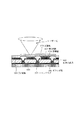
図1〜3は、実施例1に係る有機ELパネルの欠陥部修復方法を説明するもので、図1は、有機EL素子の構成を示す概略図である。図1に示すように、アクティブマトリックス基板であるガラス基板101上に有機EL素子を駆動するためのトランジスタ102を形成し、トランジスタ102の起伏を平坦化するための平坦化膜103としてアクリル樹脂をスピンコートにより被覆した。その直上には第1電極104としてCrを70nm、DCマグネトロンスパッタ法により成膜し、さらにその上には画素分離膜105としてポリイミド樹脂をスピンコートにより被覆した。これらの膜には通常のフォトリソグラフィー法によりコンタクトホール、第1電極104間の分離などを随時、各工程においてパターニングされる。この時、形成したパターンは画素数160×120ドット、画素ピッチ0.25×0.25mmである。
1 to 3 illustrate a method for repairing a defective portion of an organic EL panel according to Example 1, and FIG. 1 is a schematic diagram illustrating a configuration of an organic EL element. As shown in FIG. 1, a transistor 102 for driving an organic EL element is formed on a glass substrate 101 which is an active matrix substrate, and acrylic resin is spun as a
本実施例においては本発明の効果を明確にするため、第1電極104の表面上にパーティクルを想定して直径0.5μmの標準粒子を散布した。 In this example, in order to clarify the effect of the present invention, standard particles having a diameter of 0.5 μm were dispersed on the surface of the first electrode 104 assuming particles.
ガラス基板101は、画素数160×120(デルタ配列)、画素ピッチ0.25×0.25mmのアクティブマトリックス基板を使用した。 As the glass substrate 101, an active matrix substrate having 160 × 120 pixels (delta arrangement) and a pixel pitch of 0.25 × 0.25 mm was used.
以上の工程後に真空高温炉において脱水処理を施した。脱水処理条件は減圧下10Pa、炉内温度200℃にて処理時間0.5〜3hrの範囲で施した。次にドライエア雰囲気下において紫外光を10分程度照射した。 After the above steps, dehydration treatment was performed in a vacuum high-temperature furnace. The dehydration conditions were 10 Pa under reduced pressure and a furnace temperature of 200 ° C. for a treatment time of 0.5 to 3 hours. Next, ultraviolet light was irradiated for about 10 minutes in a dry air atmosphere.
さらに作成したアクティブマトリックス基板を真空層に移し、以下のように有機EL素子を作製する。 Furthermore, the created active matrix substrate is moved to a vacuum layer, and an organic EL element is produced as follows.
正孔注入層、発光層、電子輸送層、電子注入層からなる有機層106を抵抗加熱式蒸着法にて成膜した。この時の、赤色発光画素、緑色発光画素、青色発光画素の各有機層の膜厚を、図4の表1に示す。発光層のみ膜厚に変化を与えており、光の取り出し効率を考慮して表1のような構成となっている。続いて、第2電極107としてITOをDCマグネトロンスパッタ法によって70nm成膜した。次に、素子への水分防止のための保護層(保護膜)108として化学気相成長法(CVD)によりSiNxを3μm成膜した。このような工程により実施例1の有機ELパネルを作製した。 An organic layer 106 including a hole injection layer, a light emitting layer, an electron transport layer, and an electron injection layer was formed by a resistance heating vapor deposition method. Table 1 in FIG. 4 shows the film thicknesses of the organic layers of the red light emitting pixel, the green light emitting pixel, and the blue light emitting pixel at this time. Only the light emitting layer changes the film thickness, and the structure shown in Table 1 is adopted in consideration of the light extraction efficiency. Subsequently, ITO was deposited to a thickness of 70 nm as the second electrode 107 by DC magnetron sputtering. Next, 3 μm of SiNx was formed as a protective layer (protective film) 108 for preventing moisture on the element by chemical vapor deposition (CVD). The organic EL panel of Example 1 was produced through such steps.
実施例1の有機ELパネルは、光取り出し方向がガラス面とは反対のトップエミッション型の有機ELパネルである。 The organic EL panel of Example 1 is a top emission type organic EL panel whose light extraction direction is opposite to the glass surface.
このように作製した有機ELパネルを駆動し、点灯状態を確認し、非点灯画素を詳細に観察した。第1電極104の表面上に散布した直径0.5umの標準粒子が短絡部となり発生した非点灯画素は、1000画素程度であった。 The organic EL panel produced in this way was driven, the lighting state was confirmed, and non-lighting pixels were observed in detail. The number of non-lighted pixels generated by the standard particles having a diameter of 0.5 μm dispersed on the surface of the first electrode 104 serving as a short-circuit portion was about 1000 pixels.
次に有機ELパネルを図2に示す欠陥部修復装置に移し、レーザー光による欠陥部修復処理を行った。この欠陥部修復装置は、レーザー発振機202、レーザー光学系203、ステージ204、パネル駆動系205を備え、レーザー光学系付随のCCDカメラ206を介して画素の拡大像を別のモニター207により確認できる。レーザー発振機202はHOYA製、YAGレーザー波長1064nm及び532nm可変、最大出力20mJ、1パルス6nsecを使用した。出力はダイヤルによって200分割に制御される。またレーザーを減衰させるための不図示の1/2フィルターを挿入して過度のエネルギー入射を抑制するとともに、不図示のアパーチャ−によりレーザー光の照射面積を減少することが可能である。レーザー光学系は対物レンズ208、不図示の結像レンズを有し、CCDカメラ206を介して欠陥箇所の拡大像を視認するとともに、レーザー照射を可能にする機構となっている。
Next, the organic EL panel was moved to the defect repair apparatus shown in FIG. 2, and a defect repair process using a laser beam was performed. This defect repair apparatus includes a
処理手順は、有機ELパネルを表面が上になるようにステージ204に積載し、非点灯画素上に対物レンズ208が位置するようステージを粗動させる。モニター207により、有機ELパネルの短絡部と思われる欠陥部にレーザー光の照準が合うようさらにステージを微調整し照射する。この時、非点灯画素位置はパネル駆動系205により点灯させて、ステージ204を動かしながらモニターで確認することも可能である。また別の観察手段によって前もって非点灯画素座標を記録しておきステージ204を粗動させることも可能である。
In the processing procedure, the organic EL panel is mounted on the
欠陥部修復の確認はパネル駆動系205により常に駆動状態にしておき、レーザー照射により点灯に切り替わるのをモニター207で確認することが可能である。またレーザー照射時には非駆動状態でレーザー照射後駆動させ点灯に切り替わるのを確認することも可能である。
It is possible to confirm that the defective portion is repaired by constantly driving the
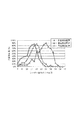
図3のグラフに示すようにレーザー出力を変化させて欠陥修復率を確認した。横軸のレーザー出力値は装置上のダイヤル値であり2ダイヤル値ずつ上昇した。縦軸の欠陥修復率は各レーザー出力ダイヤル値に対する欠陥修復率であり、各ダイヤル値に対する母数は50箇所である。また使用した波長は1064nmである。図3には赤色発光画素、緑色発光画素、青色発光画素のそれぞれの欠陥修復率を併記している。 As shown in the graph of FIG. 3, the defect repair rate was confirmed by changing the laser output. The laser output value on the horizontal axis is the dial value on the device, and increased by 2 dial values. The defect repair rate on the vertical axis is the defect repair rate for each laser output dial value, and the number of parameters for each dial value is 50. The wavelength used is 1064 nm. FIG. 3 also shows the defect repair rates of the red, green, and blue light emitting pixels.
図4の表1には得られた各発光色での最も欠陥修復率の高いレーザー出力ダイヤル値の強度比(最適レーザー強度比)を、赤色発光画素を基準にして示した。表1に示されるように各発光色の有機層の総膜厚の膜厚比とレーザー出力強度比の比率はほぼ一致し、式(1)と良く適合している。結果の考察として、各色の発光層材料のレーザー光吸収率は異なるものの支配的ではなく、有機層の総膜厚が持つ熱容量が支配的であると考える。 Table 1 in FIG. 4 shows the intensity ratio (optimum laser intensity ratio) of the laser output dial value with the highest defect repair rate in each emission color obtained, with the red light emitting pixel as a reference. As shown in Table 1, the ratio of the film thickness ratio of the total thickness of the organic layers of the respective emission colors and the ratio of the laser output intensity ratio are almost the same, and is well matched with the formula (1). As a consideration of the results, it is considered that the light absorption layer materials of the respective colors have different laser light absorptances but are not dominant, but the heat capacity of the total thickness of the organic layer is dominant.
各発光色の最適レーザー出力ダイヤル値を中心値にして±10%のダイヤル値範囲では各最大欠陥修復率から5%低下以内に入っていた。さらに膜厚比より算出する最適レーザー出力ダイヤル値はその範囲に入っていた。このように膜厚比よりレーザー強度を他色の発光画素に算出しても充分に耐えうる結果であり、各発光色の最適レーザー出力ダイヤル値を中心値にして±10%範囲内では欠陥部の修復に充分耐えうる。 Within the dial value range of ± 10% centered on the optimum laser output dial value of each luminescent color, it was within 5% of each maximum defect repair rate. Furthermore, the optimum laser output dial value calculated from the film thickness ratio was within that range. Thus, even if the laser intensity is calculated for the light emitting pixels of other colors based on the film thickness ratio, the results can be sufficiently tolerated, and the defect portion is within ± 10% range with the optimum laser output dial value of each light emitting color as the center value. Can withstand the repair of
上記のように実施例1で作成した有機ELパネルを高温炉にて大気圧・温度60℃・湿度90%の条件で10時間保持した。その後、駆動・発光させ、欠陥修復箇所を顕微鏡により観察したが、いずれの箇所もダークスポットの発生及び成長は見られず保護膜の損傷は見られなかった。また保護膜の損傷が発生し始めるレーザー出力のダイヤル値は100以上であり、上記の各色のレーザー出力強度は保護膜の損傷にはいたらず、充分に製品として耐えうることがわかる。
As described above, the organic EL panel prepared in Example 1 was held in a high-temperature furnace for 10 hours under conditions of atmospheric pressure,
以上のように各発光色でレーザー出力の強度比は各発光色の有機層の総膜厚比で表され、良く式(1)に適合する。また一色のレーザー出力条件をだすことにより、他色のレーザー出力条件を簡易的に算出することが可能である。このようなレーザー出力条件下で有機ELパネルの欠陥部の修復を行なうことにより、高歩留まりのトップエミッション型有機ELパネルの製造方法を実現できる。 As described above, the intensity ratio of the laser output for each emission color is represented by the total film thickness ratio of the organic layers of each emission color, and well fits equation (1). In addition, by determining the laser output conditions for one color, it is possible to easily calculate the laser output conditions for the other colors. By repairing the defective portion of the organic EL panel under such laser output conditions, a method for producing a high-emission top emission organic EL panel can be realized.
第1電極の材料としてITO120nmをDCスパッタリング法により成膜したこと以外は実施例1と同様にアクティブマトリックス基板を作成し、実施例1と同様に第1電極の表面上に標準粒子を散布した。さらに実施例1と同様に脱水処理及び紫外線による表面処理を行った。 An active matrix substrate was prepared in the same manner as in Example 1 except that ITO 120 nm was formed by DC sputtering as a material for the first electrode, and standard particles were dispersed on the surface of the first electrode in the same manner as in Example 1. Further, as in Example 1, dehydration treatment and surface treatment with ultraviolet rays were performed.
また、有機層についても実施例1と同様の積層順で抵抗加熱式蒸着法により成膜し、各発光色の各層の膜厚は図5に示す表2のように作成した。第2電極は実施例1と異なり、抵抗加熱式蒸着法によりAlを100nm成膜した。次に素子への水分防止のための保護層として化学気相成長法(CVD)によりSiNxを3μm成膜した。このような形態により実施例2の有機ELパネルを作製した。実施例2の有機ELパネルは光取り出し方向がガラス面より取り出すボトムエミッション型の有機ELパネルである。 Also, the organic layer was formed by resistance heating vapor deposition in the same stacking order as in Example 1, and the film thickness of each layer of each emission color was prepared as shown in Table 2 shown in FIG. Unlike Example 1, the second electrode was formed by depositing Al with a thickness of 100 nm by resistance heating vapor deposition. Next, 3 μm of SiNx was formed by chemical vapor deposition (CVD) as a protective layer for preventing moisture on the device. The organic EL panel of Example 2 was produced according to such a form. The organic EL panel of Example 2 is a bottom emission type organic EL panel whose light extraction direction is extracted from the glass surface.
次に実施例1と同様の評価方法でレーザー出力を可変させて各発光色での欠陥修復率を確認した。この時実施例1とは異なりレーザー光は基板面より入射した。最適のレーザー出力ダイヤル値と赤色発光画素を基準にした強度比を図5の表2に併せて示した。表2に示される強度比と各色の有機層の総膜厚の膜厚比との比率はほぼ一致し、式(1)と良く適合している。 Next, the laser output was varied by the same evaluation method as in Example 1, and the defect repair rate in each emission color was confirmed. At this time, unlike Example 1, the laser light was incident from the substrate surface. The optimum laser output dial value and the intensity ratio based on the red light emitting pixel are also shown in Table 2 of FIG. The ratios of the intensity ratios shown in Table 2 and the film thickness ratios of the total film thicknesses of the organic layers of the respective colors almost coincide with each other and are well matched with the formula (1).
各発光色の最適レーザー出力ダイヤル値を中心値にして±10%のダイヤル値範囲では各最大欠陥修復率から5%低下以内に入っていた。さらに膜厚比より算出する最適レーザー出力ダイヤル値はその範囲に入っていた。このように膜厚比よりレーザー強度を他色の発光画素に算出しても充分に耐えうる結果であり、各発光色の最適レーザー出力ダイヤル値を中心値にして±10%範囲内では欠陥部の修復に充分耐えうる。 Within the dial value range of ± 10% centered on the optimum laser output dial value of each luminescent color, it was within 5% of each maximum defect repair rate. Furthermore, the optimum laser output dial value calculated from the film thickness ratio was within that range. Thus, even if the laser intensity is calculated for the light emitting pixels of other colors based on the film thickness ratio, the results can be sufficiently tolerated, and the defect portion is within ± 10% range with the optimum laser output dial value of each light emitting color as the center value. Can withstand the repair of
また、実施例1と同様に欠陥修復処理を施して作成した実施例2の有機ELパネルを高温炉にて大気圧・60℃・湿度90%の条件で10時間保持した。その後、駆動・発光させて欠陥処理箇所を顕微鏡で確認したところ、いずれの箇所もダークスポットが発生しておらず保護膜の損傷は発生していない。 In addition, the organic EL panel of Example 2 prepared by performing defect repair processing in the same manner as in Example 1 was held in a high-temperature furnace for 10 hours under conditions of atmospheric pressure, 60 ° C., and humidity of 90%. After that, when the defect processing portion was confirmed with a microscope by driving and emitting light, no dark spot was generated in any portion, and the protective film was not damaged.
以上のように各発光色でレーザー出力の強度比は各発光色の有機層の総膜厚比で表され、良く式(1)と適合している。また一色のレーザー出力条件をだすことにより、他色のレーザー出力条件を簡易的に算出することが可能である。このようなレーザー出力条件下で有機ELパネルの欠陥部の修復を行うことにより、高歩留まりのボトムエミッション型有機ELパネルの製造方法を実現できる。 As described above, the intensity ratio of the laser output for each emission color is expressed by the total film thickness ratio of the organic layers of each emission color, and is well matched with the formula (1). In addition, by determining the laser output conditions for one color, it is possible to easily calculate the laser output conditions for the other colors. By repairing the defective portion of the organic EL panel under such laser output conditions, a method for manufacturing a high-emission bottom emission organic EL panel can be realized.
(比較例1)
実施例1と同じ条件で作製した有機ELパネルについて、一色の最適レーザー出力ダイヤル値で統一し、欠陥修復処理を行った場合の欠陥修復率を図6の表3に示した。いずれの出力でも高確率で欠陥修復が出来ないことがわかり、各色の有機層の総膜厚比によってレーザー出力を可変(制御)する本発明の方法が欠陥画素の修復に優れていることを示している。
(Comparative Example 1)
Table 3 in FIG. 6 shows the defect repair rate when the organic EL panel manufactured under the same conditions as in Example 1 is unified with the optimum laser output dial value of one color and the defect repair process is performed. It can be seen that defect output cannot be repaired with high probability at any output, and that the method of the present invention that varies (controls) the laser output according to the total film thickness ratio of each color organic layer is excellent in repairing defective pixels. ing.
(比較例2)
実施例2と同じ条件で作製した有機ELパネルについて、一色の最適レーザー出力ダイヤル値で統一し、欠陥修復処理を行った場合の欠陥修復率を図7の表4に示した。いずれの出力でも高確率で欠陥修復が出来ないことがわかり、各色の有機層の総膜厚比によってレーザー出力を可変(制御)する本発明の方法が欠陥画素の修復に優れていることを示している。
(Comparative Example 2)
Table 4 in FIG. 7 shows the defect repair rate when the organic EL panel manufactured under the same conditions as in Example 2 was unified with the optimum laser output dial value of one color and the defect repair process was performed. It can be seen that defect output cannot be repaired with high probability at any output, and that the method of the present invention that varies (controls) the laser output according to the total film thickness ratio of each color organic layer is excellent in repairing defective pixels. ing.
101 ガラス基板
102 トランジスタ
103 平坦化膜
104 第1電極
105 画素分離膜
106 有機層
107 第2電極
108 保護層
202 レーザー発振機
203 レーザー光学系
204 ステージ
205 パネル駆動系
206 CCDカメラ
207 モニター
DESCRIPTION OF SYMBOLS 101 Glass substrate 102
Claims (4)
前記有機層の欠陥部に、前記複数の発光色画素の発光色毎に制御された強度の光を照射する工程を有することを特徴とする有機ELパネルの欠陥部修復方法。 In the method for repairing a defective portion of an organic EL panel having an organic layer for forming a plurality of light emitting color pixels,
A method for repairing a defect portion of an organic EL panel, comprising: irradiating a defect portion of the organic layer with light having a controlled intensity for each emission color of the plurality of emission color pixels.
t1:t2:t3・・・=P1:P2:P3・・・ The total film thickness t1, t2, t3... Of the organic layer of each luminescent color pixel and the intensity ratio P1, P2, P3. 2. The defect repairing method for an organic EL panel according to claim 1, wherein the relationship is satisfied.
t1: t2: t3 ... = P1: P2: P3 ...
前記有機層の欠陥部に、前記複数の発光色画素の発光色毎に制御された強度の光を照射する工程と、を有することを特徴とする有機ELパネルの製造方法。 Forming an organic EL panel in which a first electrode, an organic layer for forming a plurality of light emitting color pixels, a second electrode and a protective film are laminated on a substrate;
Irradiating the defect portion of the organic layer with light having a controlled intensity for each emission color of the plurality of emission color pixels.
Priority Applications (1)
| Application Number | Priority Date | Filing Date | Title |
|---|---|---|---|
| JP2007206111A JP2009043502A (en) | 2007-08-08 | 2007-08-08 | Method of repairing defective portion in organic electroluminescent panel |
Applications Claiming Priority (1)
| Application Number | Priority Date | Filing Date | Title |
|---|---|---|---|
| JP2007206111A JP2009043502A (en) | 2007-08-08 | 2007-08-08 | Method of repairing defective portion in organic electroluminescent panel |
Publications (2)
| Publication Number | Publication Date |
|---|---|
| JP2009043502A true JP2009043502A (en) | 2009-02-26 |
| JP2009043502A5 JP2009043502A5 (en) | 2010-09-16 |
Family
ID=40444046
Family Applications (1)
| Application Number | Title | Priority Date | Filing Date |
|---|---|---|---|
| JP2007206111A Pending JP2009043502A (en) | 2007-08-08 | 2007-08-08 | Method of repairing defective portion in organic electroluminescent panel |
Country Status (1)
| Country | Link |
|---|---|
| JP (1) | JP2009043502A (en) |
Citations (8)
| Publication number | Priority date | Publication date | Assignee | Title |
|---|---|---|---|---|
| JPH05249657A (en) * | 1992-03-05 | 1993-09-28 | Nec Corp | Photomask correcting device and method |
| JPH0982803A (en) * | 1995-09-20 | 1997-03-28 | Nec Corp | Method and device for formation of via hole |
| JP2000208252A (en) * | 1999-01-14 | 2000-07-28 | Tdk Corp | Organic electroluminescent element |
| JP2002260857A (en) * | 2000-12-28 | 2002-09-13 | Semiconductor Energy Lab Co Ltd | Forming method of light-emitting device and thin film forming device |
| JP2003217852A (en) * | 2002-01-28 | 2003-07-31 | Toyota Industries Corp | Organic el color display |
| JP2004279639A (en) * | 2003-03-14 | 2004-10-07 | Hitachi Displays Ltd | Display device and its manufacturing method |
| JP2005019818A (en) * | 2003-06-27 | 2005-01-20 | Mitsubishi Heavy Ind Ltd | Thin film processing apparatus and processing method |
| JP2007047576A (en) * | 2005-08-11 | 2007-02-22 | Toshiba Matsushita Display Technology Co Ltd | Active matrix type display device and its pixel section |
-
2007
- 2007-08-08 JP JP2007206111A patent/JP2009043502A/en active Pending
Patent Citations (8)
| Publication number | Priority date | Publication date | Assignee | Title |
|---|---|---|---|---|
| JPH05249657A (en) * | 1992-03-05 | 1993-09-28 | Nec Corp | Photomask correcting device and method |
| JPH0982803A (en) * | 1995-09-20 | 1997-03-28 | Nec Corp | Method and device for formation of via hole |
| JP2000208252A (en) * | 1999-01-14 | 2000-07-28 | Tdk Corp | Organic electroluminescent element |
| JP2002260857A (en) * | 2000-12-28 | 2002-09-13 | Semiconductor Energy Lab Co Ltd | Forming method of light-emitting device and thin film forming device |
| JP2003217852A (en) * | 2002-01-28 | 2003-07-31 | Toyota Industries Corp | Organic el color display |
| JP2004279639A (en) * | 2003-03-14 | 2004-10-07 | Hitachi Displays Ltd | Display device and its manufacturing method |
| JP2005019818A (en) * | 2003-06-27 | 2005-01-20 | Mitsubishi Heavy Ind Ltd | Thin film processing apparatus and processing method |
| JP2007047576A (en) * | 2005-08-11 | 2007-02-22 | Toshiba Matsushita Display Technology Co Ltd | Active matrix type display device and its pixel section |
Similar Documents
| Publication | Publication Date | Title |
|---|---|---|
| US7141517B2 (en) | Method of repairing and apparatus for repairing multi-color organic light-emitting display device | |
| EP2378841B1 (en) | Organic el display and method for manufacturing same | |
| JP2008235178A (en) | Organic el display and manufacturing method therefor | |
| KR101775177B1 (en) | Method of manufacturing organic el device and method of setting laser focusing position | |
| JP2010093068A (en) | Organic el display device and method of manufacturing the same | |
| JP2000012220A (en) | Manufacture of organic el display panel | |
| JP2005166635A (en) | Organic electroluminescent display device and thermal transfer donor film used for production of the same | |
| US8062085B2 (en) | Method of producing organic light emitting device | |
| JP2008235177A (en) | Manufacturing method of organic el display, and organic el display | |
| JP2008108482A (en) | Organic el display device | |
| KR20040034417A (en) | Organic electroluminescent device, method for manufacturing the organic electroluminescent device, and organic electroluminescent display apparatus | |
| JP2002252087A (en) | Organic light emission display device | |
| JP2001176672A (en) | Organic electroluminescent element and its manufacturing method | |
| JP6086333B2 (en) | Method for manufacturing organic electroluminescence display device and organic electroluminescence display device | |
| US20110186819A1 (en) | Organic electroluminescence display apparatus and manufacturing method therefor | |
| US9112187B2 (en) | Organic el device and method of manufacturing organic EL device | |
| JPWO2016079957A1 (en) | Method for manufacturing organic electroluminescent element and organic electroluminescent element | |
| JP5095224B2 (en) | Color organic EL display and manufacturing method thereof | |
| JP2008268880A (en) | Method of producing organic light emitting device | |
| JP2003264073A (en) | Manufacturing method of organic el display | |
| JP2008108590A (en) | Organic el element and its manufacturing method | |
| JP2009043502A (en) | Method of repairing defective portion in organic electroluminescent panel | |
| JP4635488B2 (en) | ORGANIC LIGHT EMITTING ELEMENT, MANUFACTURING METHOD THEREOF, AND DISPLAY DEVICE | |
| JP2011183249A (en) | Cleaning device for vapor deposition mask | |
| JP2010244866A (en) | Organic el display device |
Legal Events
| Date | Code | Title | Description |
|---|---|---|---|
| RD03 | Notification of appointment of power of attorney |
Free format text: JAPANESE INTERMEDIATE CODE: A7423 Effective date: 20090527 |
|
| A521 | Request for written amendment filed |
Free format text: JAPANESE INTERMEDIATE CODE: A523 Effective date: 20100802 |
|
| A621 | Written request for application examination |
Free format text: JAPANESE INTERMEDIATE CODE: A621 Effective date: 20100802 |
|
| A977 | Report on retrieval |
Free format text: JAPANESE INTERMEDIATE CODE: A971007 Effective date: 20111216 |
|
| A131 | Notification of reasons for refusal |
Free format text: JAPANESE INTERMEDIATE CODE: A131 Effective date: 20111220 |
|
| RD03 | Notification of appointment of power of attorney |
Free format text: JAPANESE INTERMEDIATE CODE: A7423 Effective date: 20120203 |
|
| A521 | Request for written amendment filed |
Free format text: JAPANESE INTERMEDIATE CODE: A523 Effective date: 20120220 |
|
| A02 | Decision of refusal |
Free format text: JAPANESE INTERMEDIATE CODE: A02 Effective date: 20120626 |