JP4635488B2 - ORGANIC LIGHT EMITTING ELEMENT, MANUFACTURING METHOD THEREOF, AND DISPLAY DEVICE - Google Patents
ORGANIC LIGHT EMITTING ELEMENT, MANUFACTURING METHOD THEREOF, AND DISPLAY DEVICE Download PDFInfo
- Publication number
- JP4635488B2 JP4635488B2 JP2004193591A JP2004193591A JP4635488B2 JP 4635488 B2 JP4635488 B2 JP 4635488B2 JP 2004193591 A JP2004193591 A JP 2004193591A JP 2004193591 A JP2004193591 A JP 2004193591A JP 4635488 B2 JP4635488 B2 JP 4635488B2
- Authority
- JP
- Japan
- Prior art keywords
- electrode
- layer
- organic
- light emitting
- organic light
- Prior art date
- Legal status (The legal status is an assumption and is not a legal conclusion. Google has not performed a legal analysis and makes no representation as to the accuracy of the status listed.)
- Expired - Fee Related
Links
Images


Landscapes
- Electroluminescent Light Sources (AREA)
Description
本発明は、基板上に、第1電極、発光層を含む1層以上の有機層および第2電極を順に有し、発光層で発生した光を第2電極の側から取り出す、いわゆる上面発光の有機発光素子およびその製造方法並びにこれを用いた表示装置に関する。 The present invention includes a first electrode, one or more organic layers including a light emitting layer, and a second electrode in order on a substrate, and takes out light generated in the light emitting layer from the second electrode side, so-called top emission. The present invention relates to an organic light emitting device, a method for manufacturing the same, and a display device using the same.
近年、フラットパネルディスプレイの一つとして、有機発光素子を用いた有機発光ディスプレイが注目されている。有機発光ディスプレイは、自発光型であるので視野角が広く、消費電力が低いという特性を有し、また、高精細度の高速ビデオ信号に対しても十分な応答性を有するものと考えられており、実用化に向けて開発が進められている。 In recent years, an organic light emitting display using an organic light emitting element has attracted attention as one of flat panel displays. Organic light-emitting displays are self-luminous, have a wide viewing angle and low power consumption, and are considered to be sufficiently responsive to high-definition high-speed video signals. Development is underway for practical application.
このような有機発光ディスプレイに用いられる有機発光素子としては、例えば、基板上に、第1電極、発光層を含む1層以上の有機層および第2電極を順に積層した構成のものが知られている。また、アクティブマトリクス表示を行う有機発光ディスプレイでは、基板上にTFT(Thin Film Transistor;薄膜トランジスタ)およびこのTFTを覆う平坦化絶縁膜が形成されており、この平坦化絶縁膜の上に第1電極が形成されている。 As an organic light-emitting element used in such an organic light-emitting display, for example, one having a configuration in which a first electrode, one or more organic layers including a light-emitting layer, and a second electrode are sequentially stacked on a substrate is known. Yes. Further, in an organic light emitting display that performs active matrix display, a TFT (Thin Film Transistor) and a planarization insulating film that covers the TFT are formed on a substrate, and a first electrode is formed on the planarization insulating film. Is formed.
有機発光ディスプレイでは、発光しない画素があると表示品質が著しく低下するので、製造工程において発光しない欠陥素子の発生を抑えることが必要とされている。発光しない欠陥素子が生じる原因の一つとして、製造工程において第1電極上に異物が付着するということが考えられるが、有機層を形成する前に第1電極に異物が付着することを完全に防止することは困難である。そこで、例えば特許文献1では、基板を加熱処理することにより有機層を融解させて異物を被覆してしまうようにしている。また、例えば特許文献2では、正孔輸送層を形成したのちに基板を加熱することにより、正孔輸送層の膜質を改善して欠陥素子を減少させることが提案されている。
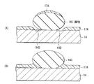
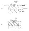
しかしながら、これらの特許文献1または特許文献2に記載されたように基板を加熱して有機層を流動させるという方法を上面発光型の有機発光素子に適用した場合、画素内の発光むらという問題が生じるおそれがある。アクティブマトリクス表示を行う上面発光型の有機発光ディスプレイでは、光を基板側から取り出す下面発光の場合とは異なり、第1電極の下にも自由にTFTを配置することができ、下面発光では実現が難しいTFT回路を構成することが可能である。しかし、この場合、例えば図23(A)に示したように、基板111上にTFT112および平坦化絶縁膜113を形成し、その上に第1電極114を形成することになるので、第1電極114にはTFT112の形状を反映した凹凸部114Aが存在することになる。このような凹凸部114Aのある第1電極114上に正孔注入層117Aを形成し、加熱すると、図23(B)に示したように、正孔注入層117Aが流動して第1電極114の凹凸部114Aに集中する傾向がある。その結果、正孔注入層117Aに著しい厚みむらが生じてしまう。よって、素子の完成後に第1電極と第2電極との間に電位差を与えたときに、正孔注入層の薄い部分では厚い部分よりも発光が強くなり、画素内の輝度むらの原因となる。更に、画素内の一部が優先的に発光するので、信頼性にも影響を与えるおそれがある。
However, when the method of heating the substrate and flowing the organic layer as described in Patent Document 1 or Patent Document 2 is applied to a top-emitting organic light-emitting element, there is a problem of uneven light emission in the pixel. May occur. Unlike the case of bottom emission in which light is extracted from the substrate side, the top emission type organic light emitting display that performs active matrix display can freely arrange TFTs under the first electrode. It is possible to configure a difficult TFT circuit. However, in this case, for example, as shown in FIG. 23A, the
また、有機層は通常10nmないし数十nmと極めて薄いのに対して異物は数μm以上とかなり大きいものが多く、特許文献1に記載されたように異物全体を被覆するためには、融解させる有機層の厚みを大きくする必要がある。そのため、上面発光素子の場合には上述した画素内の発光むらの問題が生じてしまう可能性がある。 In addition, the organic layer is usually very thin as 10 nm to several tens of nm, whereas the foreign matter is often quite large, such as several μm or more, and as described in Patent Document 1, it is melted to cover the entire foreign matter. It is necessary to increase the thickness of the organic layer. Therefore, in the case of the top surface light emitting element, there is a possibility that the above-described problem of uneven light emission in the pixel may occur.
本発明はかかる問題点に鑑みてなされたもので、その目的は、画素内の発光むらを抑制して表示品質を高めることができる有機発光素子およびその製造方法並びに表示装置を提供することにある。
The present invention has been made in view of the above problems, and its object is to provide an organic light emitting device and a manufacturing method thereof display device can improve display quality by suppressing the emission-free al in pixels is there.
本発明による有機発光素子は、基板上に、駆動素子および駆動素子を覆う平坦化絶縁膜、第1電極、発光層を含む1層以上の有機層並びに第2電極を順に備え、発光層で発生した光を第2電極の側から取り出すものであって、第1電極は、表面に駆動素子の形状を反映した凹凸部を有し、有機層のうちの一つの層は、その厚みが1nm以上30nm以下であり、かつ、基板側に第1電極の凹凸部を反映した第1凹凸面を有すると共に、第2電極側に第1電極の凹凸部を反映した第2凹凸面を有し、第2凹凸面の凹部および凸部のそれぞれが平坦化されているものである。 An organic light emitting device according to the present invention includes a driving element, a planarization insulating film covering the driving element, a first electrode, one or more organic layers including a light emitting layer, and a second electrode in order, and is generated in the light emitting layer. The first electrode has a concavo-convex portion reflecting the shape of the driving element on the surface, and one of the organic layers has a thickness of 1 nm or more. and at 30nm or less, and has a first uneven surface that reflects irregularities of the first electrode on the substrate side, have a second uneven surface that reflects irregularities of the first electrode to the second electrode side, the Each of the concave and convex portions on the two concavo-convex surfaces is flattened .
本発明による有機発光素子の製造方法は、基板上に、駆動素子および駆動素子を覆う平坦化絶縁膜、第1電極、発光層を含む1層以上の有機層並びに第2電極が順に積層され、発光層で発生した光を第2電極の側から取り出す有機発光素子を製造するものであって、表面に駆動素子の形状を反映した凹凸部を有すると共に凹凸部を含めた領域に微細凹凸を有する第1電極の上に、有機層のうちの一つの層を1nm以上30nm以下の厚みで形成したのち、基板を上記有機層のうちの一つの層のガラス転移点以上の温度で加熱するようにしたものである。 In the organic light emitting device manufacturing method according to the present invention, a driving element, a planarization insulating film covering the driving element, a first electrode, one or more organic layers including a light emitting layer, and a second electrode are sequentially stacked on the substrate, An organic light emitting device for producing light emitted from the light emitting layer from the second electrode side, which has a concavo-convex portion reflecting the shape of the driving element on the surface and a fine concavo-convex portion in a region including the concavo-convex portion. After forming one of the organic layers with a thickness of 1 nm to 30 nm on the first electrode , the substrate is heated at a temperature equal to or higher than the glass transition temperature of one of the organic layers. It is a thing.
本発明による表示装置は、基板上に、上記本発明による複数の有機発光素子を有するものである。 A display device according to the present invention has a plurality of organic light emitting elements according to the present invention on a substrate.
本発明の有機発光素子および本発明の表示装置によれば、有機層のうちの一つの層が、その厚みが1nm以上30nm以下であり、かつ、基板側に第1電極の凹凸部を反映した第1凹凸面を有すると共に、第2電極側に第1電極の凹凸部を反映した第2凹凸面を有し、第2凹凸面の凹部および凸部のそれぞれが平坦化されているようにしたので、第1電極の凹凸部に応じて上記有機層のうちの一つの層の厚みむらが大きくなってしまうことがなく、厚みむらが小さくなる。よって、画素内に発光むらが生じることを抑制し、表示品質を高めることができる。
According to the organic light emitting device of the present invention and the display device of the present invention, one of the organic layers has a thickness of 1 nm or more and 30 nm or less, and the uneven portion of the first electrode is reflected on the substrate side. It has a first uneven surface, a second uneven surface that reflects irregularities of the first electrode to the second electrode side possess, and so each of the recesses and protrusions of the second uneven surface is planarized Therefore, the thickness unevenness of one of the organic layers does not increase according to the uneven portion of the first electrode, and the thickness unevenness decreases. Therefore, it is possible to suppress the occurrence of uneven light emission in the pixel and improve the display quality.
本発明の有機発光素子の製造方法によれば、表面に駆動素子の形状を反映した凹凸部を有すると共に凹凸部を含めた領域に微細凹凸を有する第1電極の上に、有機層のうちの一つの層を1nm以上30nm以下という比較的小さな厚みで形成するようにしたので、加熱により流動した上記有機層のうちの一つの層が第1電極の凹凸部に流れ込んで厚みむらが大きくなってしまうことを抑制し、上記有機層のうちの一つの層の厚みむらを小さくすることができる。よって、画素内の発光むらが小さく、表示品質の高い有機発光素子を実現することができる。また、加熱により上記有機層のうちの一つの層を流動させることにより、第1電極に対する被覆性および密着性を高めることができる。更に、製造工程において第1電極に異物が付着したとしても、第1電極の全面を上記有機層のうちの一つの層で覆うことができ、第1電極と第2電極との短絡を防止し、表示品質を高めることができる。
According to the method for manufacturing an organic light emitting device of the present invention , the organic layer is formed on the first electrode having a concavo-convex portion reflecting the shape of the driving element on the surface and having a fine concavo-convex region in the region including the concavo-convex portion since the one layer so as to form a relatively small thickness of 1nm or 30nm or less, the thickness unevenness is large, one of the layers of the organic layer was fluidized by pressurized heat flows into the uneven portion of the first electrode The thickness unevenness of one of the organic layers can be reduced. Therefore, it is possible to realize an organic light-emitting element with small display unevenness in pixels and high display quality. Moreover, the coverage with respect to a 1st electrode and adhesiveness can be improved by making one layer of the said organic layers flow by heating. Furthermore, even if foreign matter adheres to the first electrode in the manufacturing process, the entire surface of the first electrode can be covered with one of the organic layers, and a short circuit between the first electrode and the second electrode can be prevented. , Can improve the display quality.
以下、本発明の実施の形態について図面を参照して詳細に説明する。 Hereinafter, embodiments of the present invention will be described in detail with reference to the drawings.
(第1の実施の形態)
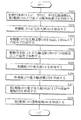
図1は、本発明の第1の実施の形態に係る有機発光素子の製造方法を表す流れ図であり、図2ないし図8および図10ないし図14は、この有機発光素子およびそれを用いた表示装置の製造方法を工程順に表す断面図である。まず、図2(A)に示したように、ガラスなどの絶縁材料よりなる駆動用基板11上に、各有機発光素子に対応する能動素子としてTFT12を形成する(ステップS101)。TFT12の構成は特に限定されず、例えばボトムゲート型でもトップゲート型でもよい。次いで、TFT12を酸化シリコンまたはPSG(Phospho-Silicate Glass)等よりなる層間絶縁膜(図示せず)で覆い、TFT12のソースおよびドレイン(いずれも図示せず)に、層間絶縁膜を介して、アルミニウム(Al)等よりなる配線(図示せず)を電気的に接続する。なお、TFT12のゲート電極(図示せず)は、図示しない走査回路に接続する。
(First embodiment)
FIG. 1 is a flowchart showing a method of manufacturing an organic light emitting device according to the first embodiment of the present invention. FIGS. 2 to 8 and FIGS. 10 to 14 show the organic light emitting device and a display using the same. It is sectional drawing showing the manufacturing method of an apparatus in order of a process. First, as shown in FIG. 2A, a
次いで、図2(B)に示したように、駆動用基板11の全面に、例えばスピンコート法により、例えばポリイミド等の有機材料よりなる平坦化絶縁膜13を形成し(ステップS101)、露光および現像により平坦化絶縁膜13を所定の形状にパターニングすると共に、配線12Bと後述する第1電極14(図3(A)参照。)とを電気的に接続するための接続孔(図示せず)を形成する。なお、平坦化絶縁膜13は、酸化シリコン(SiO2 )などにより構成するようにしてもよい。
Next, as shown in FIG. 2B, a
続いて、図3(A)に示したように、平坦化絶縁膜13の上に、例えば直流スパッタリング法により、例えばクロム(Cr)よりなる金属層を100nmの厚みで形成する。その際、スパッタガスとしては例えばアルゴン(Ar)を用い、圧力を例えば0.2Pa,出力を例えば300Wとする。そののち、この金属層を通常のリソグラフィ技術により所定の形状にパターニングし、第1電極14と、後述する第2電極18(図11参照。)の電圧降下を抑制するための補助電極15とを形成する(ステップS101)。
Subsequently, as shown in FIG. 3A, a metal layer made of, for example, chromium (Cr) is formed with a thickness of 100 nm on the
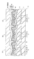
このとき、第1電極14は、表面にTFT12の形状を反映した凹凸部14Aを有している。凹凸部14Aの深さDaは例えば100nmないし1μm程度である。なお、凹凸部14Aは、平坦化絶縁膜13を設けることにより多少緩和することは可能であるが、第1電極14の下にTFT12を形成する限りは凹凸部14Aを完全に平坦化することは困難である。
At this time, the
更に、第1電極14は、図4に拡大して示したように、凹凸部14Aを含めた領域内に微細凹凸14Bが生じている。微細凹凸14Bは、第1電極14の構成材料に起因して生じる、いわば膜の凹凸であって、その深さDbは例えば10nm程度と極めて小さなものである。
Furthermore, as shown in the enlarged view of FIG. 4, the
第1電極14および補助電極15を形成したのち、図3(B)に示したように、駆動用基板11の全面にわたり、例えばCVD(Chemical Vapor Deposition ;化学的気相成長)法により、例えば酸化シリコンよりなる素子分離絶縁膜16を600nmの厚みで成膜する(ステップS101)。続いて、例えばリソグラフィ技術を用いて素子分離絶縁膜16のうち発光領域に対応する部分および補助電極15の上面を覆う部分を選択的に除去し、開口部16A,16Bを形成する。
After forming the
次に、第1電極14、素子分離絶縁膜16および補助電極15の上に、例えば蒸着法により、有機層17を形成する。その際、図5に示したように、各発光領域に対応して開口21Aを有する金属性のエリアマスク21を用い、素子分離絶縁膜16の開口部16A内の発光領域となる部分のみに有機層17を成膜する。なお、開口部16A内のみに有機層17を成膜することは難しいので、開口部16Aだけでなくその周囲にも有機層17を成膜するようにしてもよい。また、有機層17は、発光層を含む複数の層の積層構造であり、各層の材料をそれぞれ例えば0.2gずつ抵抗加熱用のボートに充填し、真空蒸着装置(図示せず)の所定の電極に取り付けたのち、真空蒸着装置内の真空槽(図示せず)内を例えば1.0×10⁻⁴Paまで減圧し、各ボートに電圧を印加し、順次加熱することにより蒸着を行う。
Next, the
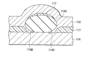
具体的には、有機層17は例えば以下のようにして形成することができる。まず、図6に示したように、第1電極14の直上に、真空蒸着法により、例えば4,4′,4″−トリス(3−メチルフェニルフェニルアミノ)トリフェニルアミン(m−MTDATA)よりなる正孔注入層17Aを1nm以上30nm以下、例えば20nmという比較的小さな厚みで形成する(ステップS102)。更に、正孔注入層17Aの厚みは、5nm以上20nm以下とすればより好ましい。より高い効果が得られるからである。このとき、正孔注入層17Aは、図7(A)に拡大して示したように、駆動用基板11側および表側のいずれも第1電極14の凹凸部14Aおよび微細凹凸14Bの両方を反映した第1凹凸面P1となっている。
Specifically, the
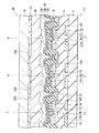
次いで、駆動用基板11を真空中または窒素(N2 )などの不活性気体雰囲気中に取り出し、例えばホットプレートまたは真空ベーク炉を用いて、駆動用基板11を正孔注入層17Aのガラス転移点以上の温度で例えば10分間加熱する(ステップS103)。加熱温度は、正孔注入層17Aのガラス転移点(m−MTDATAでは79℃)以上正孔注入層17Aの蒸発または分解温度(m−MTDATAでは205℃)より低い温度とすることが好ましく、具体的には、例えばガラス転移点より5℃程度高い温度とすることが好ましい。このとき、本実施の形態では、正孔注入層17Aを1nm以上30nm以下という比較的小さな厚みで形成するようにしたので、加熱により流動した正孔注入層17Aが第1電極14の凹凸部14Aに流れ込んで厚みむらが大きくなってしまうことを抑制することができる。その結果、加熱された後の正孔注入層17Aは、図7(B)に拡大して示したように、駆動用基板11側に第1電極14の凹凸部14Aおよび微細凹凸14Bを反映した第1凹凸面P1を有する一方、表側には第1電極14の凹凸部14Aを反映した第2凹凸面P2を有し、第2凹凸面P2の凹部P2Aおよび凸部P2Bのそれぞれは平坦化されている。よって、第1電極14の凹凸部14Aに応じて正孔注入層17Aの厚みむらが大きくなってしまうことがなく、厚みむらを小さくすることができる。よって、画素内の発光むらを小さくして、表示品質を向上させることができる。また、正孔注入層17Aの第1電極14に対する密着性を高めることができる。
Next, the driving
これに対して従来では、図23を参照して説明したように、正孔注入層117Aが厚いと、加熱により流動して第1電極114の凹凸部114Aに集中し、正孔注入層117Aに著しい厚みむらが生じてしまうおそれがあった。よって、素子の完成後に第1電極と第2電極との間に電位差を与えたときに、正孔輸送層の薄い部分では厚い部分よりも発光が強くなり、画素内の輝度むらの原因となっていた。
In contrast, conventionally, as described with reference to FIG. 23, when the
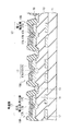
また、本実施の形態では、第1電極14上に異物14Cが付着した状態で正孔注入層117Aを形成した場合、図8(A)に拡大して示したように、異物14Cに近づくにしたがって正孔注入層17Aの厚みが薄くなっていき、異物14Cの周辺に正孔注入層17Aが形成されず第1電極14が剥き出しになった領域14Dが生じる。次いで、駆動用基板11を正孔注入層17Aのガラス転移点以上の温度で加熱することにより、図8(B)に示したように、正孔注入層17Aが流動し、毛細管現象により異物14Cの周辺に侵入し、第1電極14の全面が正孔注入層17Aで覆われる。よって、従来のように異物14C全体を正孔注入層17Aで包み込まなくても、第1電極14の全面を正孔注入層17Aで覆うことができ、第1電極14と第2電極18との短絡を防止し、表示品質を高めることができる。なお、異物14Cが金属性のものであった場合でも、異物14Cと第1電極14との接触面積は極めて小さく、また、加熱による毛細管現象により異物14Cと第1電極14との接触面積は更に小さくなるので、表示品質に与える影響はほとんどないと考えられる。
Further, in this embodiment, when the
これに対して、従来では、図9に示したように、異物114Cの周辺に有機層117が形成されないままになり、第1電極114が剥き出しになった領域114Dに第2電極118が形成されて第1電極114と第2電極118とが短絡し、欠陥素子となってしまっていた。
In contrast, conventionally, as shown in FIG. 9, the
駆動用基板11を正孔注入層17Aのガラス転移点以上の温度で加熱したのち、駆動用基板11を真空蒸着装置に戻し、図10に示したように、有機層17の他の層を形成する。すなわち、まず、正孔注入層17A上に、例えば、α−ナフチルフェニルジアミン(α−NPD)よりなる正孔輸送層17Bを30nmの厚みで形成する(ステップS104)。
After the driving
次いで、同じく図10に示したように、正孔輸送層17B上に、発光層17Cを形成する(ステップS105)。発光層17Cは、例えば、有機発光素子の発光色ごとに構成を異ならせ、各色別に形成する。赤色の光を発生する有機発光素子10Rの発光層17Cは、例えば、8−キノリノールアルミニウム錯体(Alq3 )に4−ジシアノメチレン−6−(p−ジメチルアミノスチリル)−2−メチル−4H−ピラン(DCM)を2体積%混合したものにより構成し、厚みを40nm程度とする。緑色の光を発生する有機発光素子10Gの発光層17Cは、例えば、Alq3 により構成し、厚みを50nm程度とする。青色の光を発生する有機発光素子10Bの発光層17Cは、例えば、バソクプロイン(BCP)により構成し、厚みを15nm程度とする。
Next, as shown in FIG. 10, the
続いて、同じく図10に示したように、有機発光素子の発光色により必要に応じて電子輸送層17Dを形成する(ステップS106)。例えば、有機発光素子10R,10Gでは電子輸送層17Dを形成しないが、有機発光素子10Bの発光層17C上には、例えば、Alq3 よりなる電子輸送層17Dを30nm程度の厚みで形成する。
Subsequently, as shown in FIG. 10 as well, an electron transport layer 17D is formed according to the emission color of the organic light emitting element as required (step S106). For example, the electron transport layer 17D is not formed in the organic
有機層17の他の層を形成したのち、図11に示したように、有機層17上に、例えば、電子注入層18A,発光層17Cで発生した光に対して半透過性を有する半透過性電極18B,およびこの半透過性電極18Bの電気抵抗を下げるための透明電極18Cを順に形成し、第2電極18を形成する。これにより、第2電極18と補助電極15とが電気的に接続される。
After the other layers of the
具体的には、まず、有機層17上に、例えば蒸着法により、例えばフッ化リチウム(LiF)よりなる電子注入層18Aを1nmの厚みで形成する(ステップS107)。
Specifically, first, an
次いで、例えば蒸着法により、例えばマグネシウム(Mg)−銀(Ag)合金よりなる半透過性電極18Bを10nmの厚みで形成する(ステップS107)。その際、例えば、半透過性電極18Bを構成する例えばマグネシウムおよび銀を、例えば別々の抵抗加熱用のボートにマグネシウムを1g、銀を0.2gそれぞれ充填して、真空蒸着装置(図示せず)の所定の電極に取り付ける。次いで、真空蒸着装置内の真空槽(図示せず)内の雰囲気を例えば1.0×10⁻⁴Paまで減圧したのち、各抵抗加熱用のボートに電圧を印加し、加熱して、マグネシウムと銀とを共蒸着させる。マグネシウムと銀との成長速度比は、例えば9:1とする。
Next, a
半透過性電極18Bを形成したのち、例えば直流スパッタリングにより、透明電極18Cを100nmの厚みで形成する(ステップS108)。透明電極18Cの構成材料としては、例えば、インジウム酸化物(InOx ),スズ酸化物(SnOx )および亜鉛酸化物(ZnOx )のうちの少なくとも1種を含むものを用いることが好ましい。具体的には、例えば、インジウムと亜鉛(Zn)と酸素とを含む化合物(IZO;Indium Zinc Oxide )が好ましい。室温で成膜しても良好な導電性および高い透過率を得ることができるからである。スパッタガスとしては例えばアルゴンと酸素との混合ガス(体積比Ar:O2 =1000:5)を用い、圧力は例えば0.3Pa、出力は例えば200Wとする。
After forming the
以上により、駆動用基板11上に本実施の形態に係る有機発光素子10R,10G,10Bを有する駆動パネル10が完成する。なお、必要に応じて、第2電極18の上に保護膜(図示せず)を設けてもよい。この保護膜は、例えば、酸化シリコンまたは窒化シリコン(SiN)などの透明誘電体により構成し、厚みを500nm以上10000nm以下とする。
As described above, the
また、図12(A)に示したように、例えば、有機発光素子10R,10G,10Bで発生した光に対して透明なガラスなどの材料よりなる封止用基板31の上に、赤色フィルタ32Rの材料として例えば顔料を混入した樹脂をスピンコートなどにより塗布し、フォトリソグラフィ技術によりパターニングして焼成することにより赤色フィルタ32Rを形成する。続いて、図12(B)に示したように、赤色フィルタ32Rと同様にして、青色フィルタ32Bおよび緑色フィルタ32Gを順次形成する。これにより、封止パネル30が形成される。
Further, as shown in FIG. 12A, for example, a
封止パネル30および駆動パネル10を形成したのち、図13に示したように、駆動用基板11の有機発光素子10R,10G,10Bを形成した側に、熱硬化型樹脂よりなる接着層40を塗布形成する。塗布は、例えば、スリットノズル型ディスペンサーから樹脂を吐出させて行うようにしてもよく、ロールコートあるいはスクリーン印刷などにより行うようにしてもよい。次いで、図14に示したように、駆動パネル10と封止パネル30とを接着層40を介して貼り合わせる。その際、封止パネル30のうちカラーフィルタ32を形成した側の面を、駆動パネル10と対向させて配置することが好ましい。また、接着層40に気泡などが混入しないようにすることが好ましい。そののち、封止パネル30のカラーフィルタ32と駆動パネル10の有機発光素子10R,10G,10Bとの相対位置を整合させてから所定温度で所定時間加熱処理を行い、接着層40の熱硬化性樹脂を硬化させる。以上により、本実施の形態に係る表示装置が完成する。
After forming the sealing
この表示装置では、例えば、第1電極14と第2電極18との間に所定の電圧が印加されると、有機層17の発光層17Cに電流が注入され、正孔と電子とが再結合することにより光が発生する。この光は第2電極18,接着層40および封止パネル30を透過して取り出される。ここでは、有機層17の正孔注入層17Aが、図7(B)に示したように、駆動用基板11側に第1電極14の凹凸部14Aおよび微細凹凸14Bを反映した第1凹凸面P1を有する一方、第2電極18側に第1電極14の凹凸部14Aを反映した第2凹凸面P2を有し、この第2凹凸面P2の凹部P2Aおよび凸部P2Bのそれぞれが平坦化されているようにしたので、第1電極14にTFT12の形状を反映した凹凸部14Aがある場合でも、その凹凸部14Aに応じて正孔注入層17Aの厚みむらが大きくなってしまうことがなく、厚みむらが小さくなっている。よって、画素内に発光むらが生じることが抑制され、表示品質が向上する。
In this display device, for example, when a predetermined voltage is applied between the
以上のように本実施の形態によれば、有機層17のうちの正孔注入層17Aを1nm以上30nm以下という比較的小さな厚みで形成するようにしたので、第1電極14にTFT12の形状を反映した凹凸部14Aがある場合でも、加熱により流動した正孔注入層17Aが第1電極14の凹凸部14Aに流れ込んで厚みむらが大きくなってしまうことを抑制することができる。よって、画素内の発光むらが小さく、表示品質の高い有機発光素子10R,10G,10Bを実現することができる。また、加熱により正孔注入層17Aを流動させることにより、第1電極14に対する被覆性を高めることができる。よって、製造工程において第1電極14に異物14Cが付着したとしても、第1電極14の全面を正孔注入層17Aで覆うことができ、第1電極14と第2電極18との短絡を防止し、表示品質を高めることができる。更に、正孔注入層17Aの第1電極14に対する密着性を高めることができる。
As described above, according to the present embodiment, the
(第2の実施の形態)
図15は、本発明の第2の実施の形態に係る有機発光素子の製造方法を表す流れ図である。この製造方法は、有機層17の正孔注入層17Aのガラス転移点を有機層17のうちで最も低くすると共に、有機層17のすべての層を一貫成膜したのちに、駆動用基板11を正孔注入層17Aのガラス転移点以上の温度で加熱することが、第1の実施の形態に係る有機発光素子の製造方法とは異なるものである。なお、第1の実施の形態と製造工程が重複する部分については、図2ないし図13を参照して説明する。
(Second Embodiment)
FIG. 15 is a flowchart showing a method for manufacturing an organic light emitting device according to the second embodiment of the present invention. In this manufacturing method, the glass transition point of the
まず、第1の実施の形態と同様に、図2(A)に示した工程により、駆動用基板11上に、TFT12を形成する(ステップS101)。
First, as in the first embodiment, the
次いで、第1の実施の形態と同様に、図2(B)に示した工程により、駆動用基板11の全面に、平坦化絶縁膜13を形成し(ステップS101)、露光および現像により平坦化絶縁膜13を所定の形状にパターニングすると共に接続孔(図示せず)を形成する。
Next, as in the first embodiment, the
続いて、第1の実施の形態と同様に、図3(A)に示した工程により、平坦化絶縁膜13の上に、第1電極14および補助電極15を形成する(ステップS101)。
Subsequently, similarly to the first embodiment, the
第1電極14および補助電極15を形成したのち、第1の実施の形態と同様に、図3(B)に示した工程により、駆動用基板11の全面にわたり、素子分離絶縁膜16を形成し(ステップS101)、開口部16A,16Bを形成する。
After the
素子分離絶縁膜16を形成したのち、、第1の実施の形態と同様に、図6(A)に示した工程により、第1電極14の直上に、例えばm−MTDATAよりなる正孔注入層17Aを1nm以上30nm以下、例えば20nmという比較的小さな厚みで形成する(ステップS102)。
After the element
正孔注入層17Aを形成したのち、第1の実施の形態と同様に、図10に示した工程により、正孔輸送層17Bを形成する(ステップS104)。続いて、第1の実施の形態と同様に、図10に示した工程により、正孔輸送層17B上に、有機発光素子10R,10G,10Bのそれぞれの発光層17Cを形成する(ステップS105)。そののち、第1の実施の形態と同様に、図10に示した工程により、有機発光素子10Bの発光層17C上に電子輸送層17Dを形成する(ステップS106)。
After forming the
次いで、駆動用基板11を真空中または窒素(N2 )などの不活性気体雰囲気中に取り出し、例えばホットプレートまたは真空ベーク炉を用いて、駆動用基板11を正孔注入層17Aのガラス転移点以上の温度で例えば10分間加熱する(ステップS103)。加熱温度は、正孔注入層17Aのガラス転移点(m−MTDATAでは79℃)以上有機層17の他の層(正孔輸送層17B,発光層17Cおよび電子輸送層17D)のガラス転移点より低い温度とすることが好ましく、具体的には、例えば正孔注入層17Aのガラス転移点より5℃程度高い温度とすることが好ましい。正孔注入層17Aだけを溶融・流動させることができるからである。このとき、本実施の形態では、有機層17を一貫成膜したのちに駆動用基板11を加熱するようにしたので、製造工程を簡素化し、タクトタイムを短縮することができる。また、このように一貫成膜後に加熱する場合にも、正孔注入層17Aを1nm以上30nm以下という比較的小さな厚みで形成するので、正孔注入層17Aが第1電極14の凹凸部14Aに流れ込んで厚みむらが大きくなってしまうことを抑制することができる。なお、加熱された正孔注入層17Aは、上に正孔輸送層17Bなどの他の層があっても溶融・流動し、加熱後の正孔注入層17Aの表側は、凹部P2Aおよび凸部P2Bのそれぞれが完全に平坦にはならないが微細凹凸14Bは緩和されていると考えられる。
Next, the driving
駆動用基板11を正孔注入層17Aのガラス転移点以上の温度で加熱したのち、第1の実施の形態と同様に、図11に示した工程により、有機層17上に、第2電極18の電子注入層18Aおよび半透過性電極18Bを順に形成する(ステップS107)。続いて、第1の実施の形態と同様に、同じく図11に示した工程により、透明電極18Cを形成する(ステップS108)。
After the driving
以上により、駆動用基板11上に本実施の形態に係る有機発光素子10R,10G,10Bを有する駆動パネル10が完成する。そののち、第1の実施の形態と同様に、図12ないし図14に示した工程により、この有機発光素子10R,10G,10Bを用いた表示装置を形成する。
As described above, the
このように本実施の形態では、有機層17の正孔注入層17A,正孔輸送層17B,発光層17Cおよび電子輸送層17Dを順に一貫成膜したのちに、駆動用基板11を正孔注入層17Aのガラス転移点以上の温度で加熱するようにしたので、製造工程を簡素化し、タクトタイムを短縮することができる。
As described above, in this embodiment, the
(第2の実施の形態の変形例)
なお、駆動用基板11を正孔注入層17Aのガラス転移点以上の温度で加熱する工程は、正孔注入層17Aを形成した後のいずれかの時点で行えばよい。したがって、例えば図16に示したように、有機層17の正孔注入層17A,正孔輸送層17B,発光層17Cおよび電子輸送層17Dを順に一貫成膜し(ステップS102,S104,S105,S106)、次いで、第2電極18の電子注入層18Aおよび半透過性電極18Bを形成したのちに(ステップS107)、駆動用基板11を正孔注入層17Aのガラス転移点以上の温度で加熱し(ステップS103)、そののち透明電極18Cを形成する(ステップS108)ようにしてもよい。これにより、蒸着法による有機層17から半透過性電極18Bまでの成膜を一貫して行うことができ、製造工程をより簡素化し、タクトタイムを更に短縮することができる。
(Modification of the second embodiment)
Note that the step of heating the driving
(第3の実施の形態)
図17は、本発明の第3の実施の形態に係る有機発光素子の製造方法を表す流れ図である。この製造方法は、有機層17の正孔輸送層17Bのガラス転移点を有機層17のうちで最も低くすると共に、有機層17の正孔注入層17Aおよび正孔輸送層17Bを形成したのちに、駆動用基板11を正孔輸送層17Bのガラス転移点以上の温度で加熱することが、第1の実施の形態に係る有機発光素子の製造方法とは異なるものである。なお、第1の実施の形態と製造工程が重複する部分については、図2ないし図14を参照して説明する。
(Third embodiment)
FIG. 17 is a flowchart showing a method for manufacturing an organic light emitting device according to the third embodiment of the invention. In this manufacturing method, the glass transition point of the
まず、第1の実施の形態と同様に、図2(A)ないし図3(B)に示した工程により、駆動用基板11上に、TFT12,平坦化絶縁膜13,第1電極14および補助電極15素子分離絶縁膜16を形成する(ステップS201)。
First, as in the first embodiment, the
素子分離絶縁膜16を形成したのち、第1電極14上に、例えば真空蒸着法により、例えば銅フタロシアニンよりなる正孔注入層17Aを20nmの厚みで形成する(ステップS202)。
After the element
正孔注入層17Aを形成したのち、例えばα−NPDよりなる正孔輸送層17Bを1nm以上30nm以下、例えば30nmの厚みで形成する(ステップS203)。
After forming the
次いで、駆動用基板11を真空中または窒素(N2 )などの不活性気体雰囲気中に取り出し、例えばホットプレートまたは真空ベーク炉を用いて、駆動用基板11を正孔輸送層17Bのガラス転移点以上の温度で例えば10分間加熱する(ステップS204)。加熱温度は、正孔輸送層17Bのガラス転移点(α−NPDでは96℃)以上有機層17の他の層(既に形成されている正孔注入層17A)のガラス転移点より低い温度とすることが好ましく、具体的には、例えば正孔輸送層17Bのガラス転移点より5℃程度高い温度とすることが好ましい。正孔輸送層17Bだけを溶融・流動させることができるからである。なお、正孔注入層17Aの銅フタロシアニンはガラス転移点を有さず、高温でも安定な物質であるため、上述した加熱温度では溶融・流動することはない。このとき、本実施の形態では、正孔輸送層17Bを1nm以上30nm以下という比較的小さな厚みで形成するようにしたので、加熱により流動した正孔輸送層17Bが第1電極14の凹凸部14Aに流れ込んで厚みむらが大きくなってしまうことを抑制することができる。よって、第1電極14の凹凸部14Aに応じて正孔輸送層17Bの厚みむらが大きくなってしまうことがなく、厚みむらを小さくすることができる。よって、画素内の発光むらを小さくして、表示品質を向上させることができる。また、正孔輸送層17Bの正孔注入層17Aまたは第1電極14に対する密着性を高めることができる。
Next, the
駆動用基板11を正孔輸送層17Bのガラス転移点以上の温度で加熱したのち、続いて、第1の実施の形態と同様に、図10に示した工程により、正孔輸送層17B上に、有機発光素子10R,10G,10Bのそれぞれの発光層17Cを形成する(ステップS205)。そののち、第1の実施の形態と同様に、有機発光素子10Bの発光層17C上に電子輸送層17Dを形成する(ステップS206)。
After the driving
有機層17を形成したのち、第1の実施の形態と同様に、図11に示した工程により、第2電極18の電子注入層18Aおよび半透過性電極18Bを順に形成する(ステップS207)。続いて、第1の実施の形態と同様に、同じく図11に示した工程により、透明電極18Cを形成する(ステップS208)。
After the
以上により、駆動用基板11上に本実施の形態に係る有機発光素子10R,10G,10Bを有する駆動パネル10が完成する。そののち、第1の実施の形態と同様に、図12ないし図14に示した工程により、この有機発光素子10R,10G,10Bを用いた表示装置を形成する。
As described above, the
このように本実施の形態では、正孔輸送層17Bを1nm以上30nm以下という比較的小さな厚みで形成するようにしたので、第1の実施の形態と同様の優れた効果を得ることができる。
Thus, in this embodiment, since the
(第4の実施の形態)
図18は、本発明の第4の実施の形態に係る有機発光素子の製造方法を表す流れ図である。この製造方法は、有機層17の正孔輸送層17Bのガラス転移点を有機層17のうちで最も低くすると共に、有機層17のすべての層を一貫成膜したのちに、駆動用基板11を正孔輸送層17Bのガラス転移点以上の温度で加熱することが、第1の実施の形態に係る有機発光素子の製造方法とは異なるものである。なお、第1の実施の形態と製造工程が重複する部分については、図2ないし図14を参照して説明する。
(Fourth embodiment)
FIG. 18 is a flowchart showing a method for manufacturing an organic light emitting device according to the fourth embodiment of the present invention. In this manufacturing method, the glass transition point of the
まず、第1の実施の形態と同様に、図2(A)ないし図3(B)に示した工程により、駆動用基板11上に、TFT12,平坦化絶縁膜13,第1電極14および補助電極15素子分離絶縁膜16を形成する(ステップS201)。
First, as in the first embodiment, the
素子分離絶縁膜16を形成したのち、第1電極14上に、例えば真空蒸着法により、例えば銅フタロシアニンよりなる正孔注入層17Aを20nmの厚みで形成する(ステップS202)。
After the element
正孔注入層17Aを形成したのち、例えばα−NPDよりなる正孔輸送層17Bを1nm以上30nm以下、例えば30nmの厚みで形成する(ステップS203)。
After forming the
正孔輸送層17Bを形成したのち、第1の実施の形態と同様に、図10に示した工程により、正孔輸送層17B上に、有機発光素子10R,10G,10Bのそれぞれの発光層17Cを形成する(ステップS205)。そののち、第1の実施の形態と同様に、有機発光素子10Bの発光層17C上に電子輸送層17Dを形成する(ステップS206)。
After forming the
次いで、駆動用基板11を真空中または窒素(N2 )などの不活性気体雰囲気中に取り出し、例えばホットプレートまたは真空ベーク炉を用いて、駆動用基板11を正孔注入層17Aのガラス転移点以上の温度で例えば10分間加熱する(ステップS204)。加熱温度は、正孔注入層17Aのガラス転移点(m−MTDATAでは79℃)以上有機層17の他の層(正孔輸送層17B,発光層17Cおよび電子輸送層17D)のガラス転移点より低い温度とすることが好ましく、具体的には、例えば正孔注入層17Aのガラス転移点より5℃程度高い温度とすることが好ましい。正孔注入層17Aだけを溶融・流動させることができるからである。このとき、本実施の形態では、有機層17を一貫成膜したのちに駆動用基板11を加熱するようにしたので、製造工程を簡素化し、タクトタイムを短縮することができる。
Next, the driving
駆動用基板11を正孔注入層17Aのガラス転移点以上の温度で加熱したのち、第1の実施の形態と同様に、図11に示した工程により、有機層17上に、第2電極18の電子注入層18Aおよび半透過性電極18Bを順に形成する(ステップS207)。続いて、第1の実施の形態と同様に、同じく図11に示した工程により、透明電極18Cを形成する(ステップS208)。
After the driving
以上により、駆動用基板11上に本実施の形態に係る有機発光素子10R,10G,10Bを有する駆動パネル10が完成する。そののち、第1の実施の形態と同様に、図12ないし図14に示した工程により、この有機発光素子10R,10G,10Bを用いた表示装置を形成する。
As described above, the
このように本実施の形態では、有機層17を一貫成膜したのちに、駆動用基板11を正孔輸送層17Bのガラス転移点以上の温度で加熱するようにしたので、製造工程を簡素化し、タクトタイムを短縮することができる。
As described above, in the present embodiment, after the
(第4の実施の形態の変形例)
なお、駆動用基板11を正孔輸送層17Bのガラス転移点以上の温度で加熱する工程は、正孔輸送層17Bの形成後から第2電極18の形成後までの間のいずれかの時点で行えばよい。したがって、例えば図19に示したように、有機層17の正孔注入層17A,正孔輸送層17B,発光層17Cおよび電子輸送層17Dを順に一貫成膜し(ステップS202,S203,S205,S206)、第2電極18の電子注入層18Aおよび半透過性電極18Bを形成したのちに(ステップS207)、駆動用基板11を正孔輸送層17Bのガラス転移点以上の温度で加熱し(ステップS204)、そののち透明電極18Cを形成する(ステップS208)ようにしてもよい。これにより、蒸着法による有機層17から半透過性電極18Bまでの成膜を一貫して行うことができ、製造工程をより簡素化し、タクトタイムを更に短縮することができる。
(Modification of the fourth embodiment)
Note that the step of heating the driving
更に、本発明の具体的な実施例について説明する。 Furthermore, specific examples of the present invention will be described.
(実施例1)
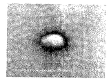
上記第1の実施の形態と同様にして駆動用基板11上に有機発光素子10Gを形成した。その際、第1電極14の直上に、m−MTDATAよりなる正孔注入層17Aを20nmの厚みで形成し、駆動用基板11を正孔注入層17Aのガラス転移点よりも5℃高い温度で10分間加熱した。加熱したのち、駆動用基板11を精査して第1電極14に付着した異物14Cを発見し、その周辺の正孔注入層17Aの状態を観察した。その結果を図20に示す。
Example 1
The organic
そののち、有機層17の残りの層および第2電極18を形成し、駆動用基板11上に有機発光素子10Gを有する駆動パネル10を完成した。なお、駆動パネル10は複数作製した。得られた各駆動パネル10について発光しない欠陥画素を計数し、それに基づいて平均欠陥発生率(総画素数に対する欠陥画素数の割合)を調べたところ、0.0218であった。
After that, the remaining layer of the
(比較例1)
正孔注入層17Aを形成したのちに、駆動用基板11を正孔注入層17Aのガラス転移点以上の温度で加熱する工程を行わずに有機層17の他の層を形成したことを除いては、上記実施例1と同様にして駆動パネルを作製した。得られた比較例の駆動パネルについても、上記実施例1と同様にして平均欠陥発生率を調べたところ、0.136であった。
(Comparative Example 1)
After the
このように実施例1によれば、比較例1に比べて平均欠陥発生率を約6分の1以下に抑えることができた。すなわち、第1電極14の直上に正孔注入層17Aを20nmと比較的薄い厚みで形成したのち、駆動用基板11を正孔注入層17Aのガラス転移点以上の温度で加熱するようにすれば、欠陥素子の発生を抑制し、表示品質を高めることができることが分かった。
Thus, according to Example 1, compared with Comparative Example 1, the average defect occurrence rate could be suppressed to about 1/6 or less. That is, after the
また、図20から分かるように、加熱した後は、異物14Cの輪郭のコントラストが高くなっており、正孔注入層17Aが毛細管現象により異物14Cの周囲に集まって、厚みが大きくなっている(図8(B)参照)ことが確認された。すなわち、第1電極14の直上に正孔注入層17Aを20nmと比較的薄い厚みで形成したのち、駆動用基板11を正孔注入層17Aのガラス転移点以上の温度で加熱するようにすれば、異物14Cの周辺の第1電極14が剥き出しになっていた領域14Dを正孔注入層17Aで覆うことができ、第1電極14と第2電極18との短絡を抑制することができることが分かった。
Further, as can be seen from FIG. 20, after heating, the contrast of the outline of the foreign matter 14C is high, and the
(実施例2)
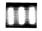
上記第1の実施の形態と同様にして駆動用基板11上に有機発光素子10Gを形成した。その際、第1電極14の直上に、m−MTDATAよりなる正孔注入層17Aを15nmの厚みで形成し、駆動用基板11を正孔注入層17Aのガラス転移点よりも5℃高い温度で10分間加熱した。そののち、有機層17の残りの層および第2電極18を形成し、駆動用基板11上に有機発光素子10Gを有する駆動パネル10を完成した。得られた駆動パネル10について、発光状態を調べた。その結果を図21に示す。
(Example 2)
The organic
(比較例2)
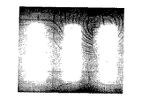
正孔注入層17Aを40nmの厚みで形成したことを除いては、実施例2と同様にして駆動パネル10を作製した。得られた駆動パネルについて、発光状態を調べた。その結果を図22に示す。
(Comparative Example 2)
The
図21および図22から分かるように、正孔注入層17Aを15nmの厚みで形成した実施例2では、画素全体がほぼ均一に光っていたのに対して、正孔注入層17Aを40nmの厚みで形成した比較例2では、画素内に発光むらが生じており、この発光むらはTFT12の形状および配置を反映したパターンを示していた。これは、比較例2では正孔注入層17Aの厚みが40nmと大きかったので、加熱により流動した正孔注入層17Aが第1電極14の凹凸部14Aに流れ込み、厚みむらが大きくなったためであると考えられる。すなわち、正孔注入層17Aを15nmという比較的小さい厚みで形成するようにすれば、画素内の発光むらを抑制して表示品質を高めることができることが分かった。
As can be seen from FIGS. 21 and 22, in Example 2 in which the
以上、実施の形態および実施例を挙げて本発明を説明したが、本発明は上記実施の形態および実施例に限定されるものではなく、種々変形が可能である。例えば、上記実施の形態および実施例において説明した各層の材料および厚み、または成膜方法および成膜条件などは限定されるものではなく、他の材料および厚みとしてもよく、または他の成膜方法および成膜条件としてもよい。例えば、有機層17は、真空蒸着法のほか、印刷法により形成するようにしてもよい。
The present invention has been described with reference to the embodiments and examples. However, the present invention is not limited to the above embodiments and examples, and various modifications can be made. For example, the material and thickness of each layer described in the above embodiments and examples, or the film formation method and film formation conditions are not limited, and other materials and thicknesses may be used, or other film formation methods. Alternatively, film forming conditions may be used. For example, the
また、例えば上記実施の形態および実施例では、第1電極14がクロムよりなる場合について説明したが、第1電極14は、クロムのほか、例えば白金(Pt),金(Au),銀(Ag)あるいはタングステン(W)などの金属元素の単体または合金により構成してもよい。また、第1電極14は単層構造でもよく複数の層の積層構造でもよい。
Further, for example, in the above-described embodiments and examples, the case where the
更に、例えば、上記実施の形態および実施例では、有機発光素子および表示装置の構成を具体的に挙げて説明したが、補助電極15などの全ての層を備える必要はなく、また、他の層を更に備えていてもよい。例えば、第2電極18において、透明電極18Cは必ずしも設ける必要はなく、電子注入層18Aおよび半透過性電極18Bのみとしてもよい。あるいは、第2電極18において、半透過性電極18Bを省略して電子注入層18Aおよび透明電極18Cのみとしてもよい。
Further, for example, in the above-described embodiments and examples, the configurations of the organic light emitting element and the display device have been specifically described, but it is not necessary to include all layers such as the
加えて、上記実施の形態および実施例においては、有機層17の構成を有機発光素子10R,10G,10Bの発光色により異ならせた場合について説明したが、有機層17を発光色にかかわらず同一構成の白色発光層とし、カラーフィルタなどにより色表示を行うようにしてもよい。
In addition, in the above-described embodiment and examples, the case where the configuration of the
更にまた、例えば、上記実施の形態および実施例では、第1電極14を陽極、第2電極18を陰極とする場合について説明したが、陽極および陰極を逆にして、第1電極14を陰極、第2電極18を陽極としてもよい。この場合、第2電極18の材料としては、金,銀,白金,銅などの単体または合金が好適である。
Furthermore, for example, in the above-described embodiments and examples, the case where the
加えてまた、上記実施の形態では、封止用基板31にカラーフィルタ32を設ける場合について説明したが、必要に応じて、ブラックマトリクスとしての反射光吸収膜を、赤色フィルタ32R,緑色フィルタ32Gおよび青色フィルタ32Bの境界に沿って設けるようにしてもよい。反射光吸収膜は、例えば黒色の着色剤を混入した光学濃度が1以上の黒色の樹脂膜、または薄膜の干渉を利用した薄膜フィルタにより構成することができる。このうち黒色の樹脂膜により構成するようにすれば、安価で容易に形成することができるので好ましい。薄膜フィルタは、例えば、金属,金属窒化物あるいは金属酸化物よりなる薄膜を1層以上積層し、薄膜の干渉を利用して光を減衰させるものである。薄膜フィルタとしては、具体的には、クロムと酸化クロム(III)(Cr2 O3 )とを交互に積層したものが挙げられる。
In addition, in the above-described embodiment, the case where the
10…駆動パネル、11…駆動用基板、12…TFT、13…平坦化絶縁膜、14…第1電極、14A…凹凸部、14B…微細凹凸、14C…異物、15…補助電極、16…素子分離絶縁膜、16A,16B…開口部、17…有機層、17A…正孔注入層、17B、正孔輸送層、17C…発光層、17D…電子輸送層、18…第2電極、18A…電子注入層、18B…半透過性電極、18C…透明電極、30…封止パネル、31…封止用基板、32…カラーフィルタ、40…接着層
DESCRIPTION OF
Claims (20)
前記第1電極は、表面に前記駆動素子の形状を反映した凹凸部を有し、
前記有機層のうちの一つの層は、その厚みが1nm以上30nm以下であり、かつ、前記基板側に前記第1電極の凹凸部を反映した第1凹凸面を有すると共に、前記第2電極側に前記第1電極の凹凸部を反映した第2凹凸面を有し、前記第2凹凸面の凹部および凸部のそれぞれが平坦化されている
有機発光素子。 A driving element, a planarization insulating film covering the driving element, a first electrode, one or more organic layers including a light emitting layer, and a second electrode are sequentially provided on a substrate, and light generated in the light emitting layer is provided in the second An organic light emitting device that is taken out from the electrode side,
The first electrode has a concavo-convex portion reflecting the shape of the driving element on the surface,
One of the organic layers has a thickness of 1 nm or more and 30 nm or less, and has a first uneven surface reflecting the uneven portion of the first electrode on the substrate side, and the second electrode side. the first have a second uneven surface that reflects irregularities of the electrode, the organic light emitting device, each being flattened in the recess and the convex portion of the second concave-convex surface.
前記有機層のうちの一つの層は、前記基板側に前記第1電極の凹凸部および微細凹凸を反映した第1凹凸面を有する
請求項1記載の有機発光素子。 The first electrode has fine irregularities in a region including the irregularities on the surface,
One layer, the organic light emitting device of claim 1 wherein the have a first uneven surface that reflects irregularities portion and the fine irregularities of the first electrode on the substrate side of the organic layer.
請求項1または請求項2記載の有機発光素子。 The organic light emitting element according to claim 1, wherein the uppermost layer of the organic layers has a third uneven surface reflecting the uneven portion of the first electrode on the second electrode side.
請求項1記載の有機発光素子。 The organic light emitting element according to claim 1, wherein one of the organic layers is formed immediately above the first electrode.
請求項1記載の有機発光素子。 The organic light emitting element according to claim 1, wherein one of the organic layers is a layer having the lowest glass transition point among the organic layers.
請求項1記載の有機発光素子。 The organic light emitting device according to claim 1, wherein one of the organic layers is a hole injection layer.
請求項1記載の有機発光素子。 The organic light emitting device according to claim 1, wherein one of the organic layers is a hole transport layer.
表面に前記駆動素子の形状を反映した凹凸部を有すると共に前記凹凸部を含めた領域に微細凹凸を有する前記第1電極の上に、前記有機層のうちの一つの層を1nm以上30nm以下の厚みで形成したのち、前記基板を前記有機層のうちの一つの層のガラス転移点以上の温度で加熱する
有機発光素子の製造方法。 A driving element, a planarization insulating film covering the driving element, a first electrode, one or more organic layers including a light emitting layer, and a second electrode are sequentially stacked on the substrate, and light generated in the light emitting layer is A method for producing an organic light-emitting element that is taken out from the two-electrode side,
On the surface of the first electrode having a concavo-convex portion reflecting the shape of the driving element and having a fine concavo-convex portion in the region including the concavo-convex portion, one layer of the organic layer is not less than 1 nm and not more than 30 nm. A method for manufacturing an organic light-emitting element, comprising forming the substrate with a thickness and then heating the substrate at a temperature equal to or higher than a glass transition point of one of the organic layers.
請求項8記載の有機発光素子の製造方法。 By heating the substrate at a temperature equal to or higher than the glass transition point of one of the organic layers, one of the organic layers has a concavo-convex portion and a fine concavo-convex portion of the first electrode on the substrate side. While having the 1st uneven surface which reflected the 2nd uneven surface which reflected the uneven part of the 1st electrode on the 2nd electrode side, each of the crevice and the convex part of the 2nd uneven surface is flattened The method for producing an organic light-emitting device according to claim 8.
請求項8記載の有機発光素子の製造方法。 The method for manufacturing an organic light-emitting element according to claim 8, wherein one of the organic layers is formed directly on the first electrode.
請求項10記載の有機発光素子の製造方法。 After forming one of the organic layers directly on the first electrode, the substrate is allowed to evaporate one of the organic layers above the glass transition point of the one of the organic layers, or The method for manufacturing an organic light-emitting element according to claim 10, wherein heating is performed at a temperature lower than a decomposition temperature, and then the other layer of the organic layer and the second electrode are formed.
請求項8記載の有機発光素子の製造方法。 The manufacturing method of the organic light emitting element of Claim 8. The glass transition point of one layer of the said organic layers is made the lowest among the said organic layers.
請求項8記載の有機発光素子の製造方法。 At any point after forming one of the organic layers, the substrate is lower than the glass transition point of one of the organic layers and lower than the glass transition point of the other layer of the organic layer. The method for producing an organic light-emitting device according to claim 8, wherein heating is performed at a temperature.
請求項8記載の有機発光素子の製造方法。 The method for manufacturing an organic light-emitting element according to claim 8, wherein the substrate is heated in vacuum or in an inert gas.
請求項8記載の有機発光素子の製造方法。 The method for manufacturing an organic light-emitting element according to claim 8, wherein the organic layer is formed by a vacuum deposition method.
請求項8記載の有機発光素子の製造方法。 The method for manufacturing an organic light-emitting element according to claim 8, wherein the organic layer is formed by a printing technique.
請求項8記載の有機発光素子の製造方法。 The method for manufacturing an organic light-emitting element according to claim 8, wherein a laminated structure of a plurality of layers including a transparent electrode is formed as the second electrode.
請求項17記載の有機発光素子の製造方法。 The method for manufacturing an organic light-emitting element according to claim 17, wherein the transparent electrode is formed by a sputtering method.
請求項17記載の有機発光素子の製造方法。 The second electrode has a laminated structure of a plurality of layers including a semi-transmissive electrode and a transparent electrode, and after the semi-transmissive electrode is formed, the glass transition point of one of the organic layers is used as the substrate. The method for manufacturing an organic light-emitting element according to claim 17, wherein heating is performed at a temperature lower than the glass transition point of the other layers of the organic layer, and then the transparent electrode is formed.
前記有機発光素子は、基板上に、駆動素子および前記駆動素子を覆う平坦化絶縁膜、第1電極、発光層を含む1層以上の有機層並びに第2電極を順に備え、前記発光層で発生した光を前記第2電極の側から取り出し、
前記第1電極は、表面に前記駆動素子の形状を反映した凹凸部を有し、
前記有機層のうちの一つの層は、その厚みが1nm以上30nm以下であり、かつ、前記基板側に前記第1電極の凹凸部を反映した第1凹凸面を有すると共に、前記第2電極側に前記第1電極の凹凸部を反映した第2凹凸面を有し、前記第2凹凸面の凹部および凸部のそれぞれが平坦化されている
表示装置。 A display device comprising a plurality of organic light emitting elements on a substrate,
The organic light emitting element includes a driving element, a planarization insulating film covering the driving element, a first electrode, one or more organic layers including a light emitting layer, and a second electrode in order, and is generated in the light emitting layer. The extracted light from the second electrode side,
The first electrode has a concavo-convex portion reflecting the shape of the driving element on the surface,
One of the organic layers has a thickness of 1 nm or more and 30 nm or less, and has a first uneven surface reflecting the uneven portion of the first electrode on the substrate side, and the second electrode side. the first have a second uneven surface that reflects irregularities of the electrode, the display respective recesses and protrusions of the second uneven surface is planarized device.
Priority Applications (1)
| Application Number | Priority Date | Filing Date | Title |
|---|---|---|---|
| JP2004193591A JP4635488B2 (en) | 2004-06-30 | 2004-06-30 | ORGANIC LIGHT EMITTING ELEMENT, MANUFACTURING METHOD THEREOF, AND DISPLAY DEVICE |
Applications Claiming Priority (1)
| Application Number | Priority Date | Filing Date | Title |
|---|---|---|---|
| JP2004193591A JP4635488B2 (en) | 2004-06-30 | 2004-06-30 | ORGANIC LIGHT EMITTING ELEMENT, MANUFACTURING METHOD THEREOF, AND DISPLAY DEVICE |
Publications (3)
| Publication Number | Publication Date |
|---|---|
| JP2006019375A JP2006019375A (en) | 2006-01-19 |
| JP2006019375A5 JP2006019375A5 (en) | 2007-06-14 |
| JP4635488B2 true JP4635488B2 (en) | 2011-02-23 |
Family
ID=35793380
Family Applications (1)
| Application Number | Title | Priority Date | Filing Date |
|---|---|---|---|
| JP2004193591A Expired - Fee Related JP4635488B2 (en) | 2004-06-30 | 2004-06-30 | ORGANIC LIGHT EMITTING ELEMENT, MANUFACTURING METHOD THEREOF, AND DISPLAY DEVICE |
Country Status (1)
| Country | Link |
|---|---|
| JP (1) | JP4635488B2 (en) |
Families Citing this family (6)
| Publication number | Priority date | Publication date | Assignee | Title |
|---|---|---|---|---|
| US8288180B2 (en) | 2005-07-04 | 2012-10-16 | Semiconductor Energy Laboratory Co., Ltd. | Method for manufacturing light emitting device |
| JP2010010333A (en) * | 2008-06-26 | 2010-01-14 | Kyocera Corp | Organic el device and method of manufacturing the same |
| JP5332396B2 (en) * | 2008-08-21 | 2013-11-06 | 株式会社デンソー | ORGANIC EL ELEMENT AND METHOD FOR PRODUCING ORGANIC EL ELEMENT |
| JP5892924B2 (en) * | 2012-12-28 | 2016-03-23 | エルジー ディスプレイ カンパニー リミテッド | Organic EL device, method for manufacturing organic EL device, and organic EL display |
| KR102067376B1 (en) * | 2013-05-21 | 2020-01-17 | 삼성디스플레이 주식회사 | Organic light emitting diode display and method for manufacturing the same |
| JP7027141B2 (en) * | 2017-12-05 | 2022-03-01 | キヤノン株式会社 | Manufacturing method of top emission type organic EL element, top emission type organic EL device, and top emission type organic EL element |
Family Cites Families (5)
| Publication number | Priority date | Publication date | Assignee | Title |
|---|---|---|---|---|
| JPH1140352A (en) * | 1997-07-11 | 1999-02-12 | Tdk Corp | Organic el element and manufacture thereof |
| JP2001068272A (en) * | 1999-08-24 | 2001-03-16 | Tdk Corp | Organic el element |
| JP2001148291A (en) * | 1999-11-19 | 2001-05-29 | Sony Corp | Display device and method of manufacturing the same |
| JP2001160486A (en) * | 1999-12-03 | 2001-06-12 | Sony Corp | Manufacturing method of organic EL display and organic EL display |
| KR100437765B1 (en) * | 2001-06-15 | 2004-06-26 | 엘지전자 주식회사 | production method of Thin Film Transistor using high-temperature substrate and, production method of display device using the Thin Film Transistor |
-
2004
- 2004-06-30 JP JP2004193591A patent/JP4635488B2/en not_active Expired - Fee Related
Also Published As
| Publication number | Publication date |
|---|---|
| JP2006019375A (en) | 2006-01-19 |
Similar Documents
| Publication | Publication Date | Title |
|---|---|---|
| KR102093628B1 (en) | Organic electro luminescent device and method of fabricating the same | |
| JP5035295B2 (en) | Organic electroluminescence display device | |
| JP5808624B2 (en) | Display device and electronic device | |
| CN100527470C (en) | Display unit and manufacturing method thereof | |
| JP2010108693A (en) | Organic el display and its manufacturing method | |
| TW201306349A (en) | Display unit and method of manufacturing same | |
| CN101789494A (en) | Organic electroluminescence device and display unit | |
| US10580988B2 (en) | Display unit and method of manufacturing display unit | |
| JP4333333B2 (en) | Display device and manufacturing method thereof | |
| CN102983281B (en) | Organic light emitting apparatus and manufacture method thereof | |
| JP4396864B2 (en) | Display device and manufacturing method thereof | |
| JP5478954B2 (en) | Organic electroluminescence display device | |
| JP2005056846A (en) | Organic electroluminescent device and manufacturing method thereof | |
| JP2010062067A (en) | Method of manufacturing display device, and display device | |
| JP2010225293A (en) | Functional element and display device | |
| JP4453385B2 (en) | Manufacturing method of display device | |
| JP4635488B2 (en) | ORGANIC LIGHT EMITTING ELEMENT, MANUFACTURING METHOD THEREOF, AND DISPLAY DEVICE | |
| JP2008311103A (en) | Display device manufacturing method and display device | |
| JP2006156267A (en) | Display device manufacturing method and display device | |
| JP2007273274A (en) | Organic EL device and manufacturing method thereof | |
| JP2011029322A (en) | Display device and method for manufacturing the same | |
| KR101605008B1 (en) | Fabrication method for organic light emitting diodes device | |
| JP2019091640A (en) | Organic el display panel, sticking sheet for window glass, and window glass | |
| JP2006338916A (en) | Organic EL element, display device, and method of manufacturing organic EL element | |
| CN105280680B (en) | Organic LED display device and its manufacturing method |
Legal Events
| Date | Code | Title | Description |
|---|---|---|---|
| A521 | Request for written amendment filed |
Free format text: JAPANESE INTERMEDIATE CODE: A523 Effective date: 20070419 |
|
| A621 | Written request for application examination |
Free format text: JAPANESE INTERMEDIATE CODE: A621 Effective date: 20070419 |
|
| A131 | Notification of reasons for refusal |
Free format text: JAPANESE INTERMEDIATE CODE: A131 Effective date: 20091125 |
|
| A521 | Request for written amendment filed |
Free format text: JAPANESE INTERMEDIATE CODE: A523 Effective date: 20100121 |
|
| A131 | Notification of reasons for refusal |
Free format text: JAPANESE INTERMEDIATE CODE: A131 Effective date: 20100216 |
|
| A521 | Request for written amendment filed |
Free format text: JAPANESE INTERMEDIATE CODE: A523 Effective date: 20100419 |
|
| A02 | Decision of refusal |
Free format text: JAPANESE INTERMEDIATE CODE: A02 Effective date: 20100630 |
|
| A521 | Request for written amendment filed |
Free format text: JAPANESE INTERMEDIATE CODE: A523 Effective date: 20100921 |
|
| A911 | Transfer to examiner for re-examination before appeal (zenchi) |
Free format text: JAPANESE INTERMEDIATE CODE: A911 Effective date: 20101007 |
|
| TRDD | Decision of grant or rejection written | ||
| A01 | Written decision to grant a patent or to grant a registration (utility model) |
Free format text: JAPANESE INTERMEDIATE CODE: A01 Effective date: 20101026 |
|
| A01 | Written decision to grant a patent or to grant a registration (utility model) |
Free format text: JAPANESE INTERMEDIATE CODE: A01 |
|
| A61 | First payment of annual fees (during grant procedure) |
Free format text: JAPANESE INTERMEDIATE CODE: A61 Effective date: 20101108 |
|
| FPAY | Renewal fee payment (event date is renewal date of database) |
Free format text: PAYMENT UNTIL: 20131203 Year of fee payment: 3 |
|
| FPAY | Renewal fee payment (event date is renewal date of database) |
Free format text: PAYMENT UNTIL: 20131203 Year of fee payment: 3 |
|
| R250 | Receipt of annual fees |
Free format text: JAPANESE INTERMEDIATE CODE: R250 |
|
| R250 | Receipt of annual fees |
Free format text: JAPANESE INTERMEDIATE CODE: R250 |
|
| LAPS | Cancellation because of no payment of annual fees |