CN101789494A - Organic electroluminescence device and display unit - Google Patents
Organic electroluminescence device and display unit Download PDFInfo
- Publication number
- CN101789494A CN101789494A CN201010001064A CN201010001064A CN101789494A CN 101789494 A CN101789494 A CN 101789494A CN 201010001064 A CN201010001064 A CN 201010001064A CN 201010001064 A CN201010001064 A CN 201010001064A CN 101789494 A CN101789494 A CN 101789494A
- Authority
- CN
- China
- Prior art keywords
- layer
- anode
- electroluminescence device
- organic electroluminescence
- alloy
- Prior art date
- Legal status (The legal status is an assumption and is not a legal conclusion. Google has not performed a legal analysis and makes no representation as to the accuracy of the status listed.)
- Pending
Links
- 238000005401 electroluminescence Methods 0.000 title claims abstract description 96
- 239000010410 layer Substances 0.000 claims abstract description 231
- 239000012044 organic layer Substances 0.000 claims abstract description 48
- 229910052782 aluminium Inorganic materials 0.000 claims abstract description 37
- XAGFODPZIPBFFR-UHFFFAOYSA-N aluminium Chemical compound [Al] XAGFODPZIPBFFR-UHFFFAOYSA-N 0.000 claims abstract description 34
- 229910045601 alloy Inorganic materials 0.000 claims abstract description 29
- 239000000956 alloy Substances 0.000 claims abstract description 29
- 239000004411 aluminium Substances 0.000 claims description 29
- 239000000463 material Substances 0.000 claims description 24
- 125000004432 carbon atom Chemical group C* 0.000 claims description 23
- 229910000838 Al alloy Inorganic materials 0.000 claims description 21
- PXHVJJICTQNCMI-UHFFFAOYSA-N Nickel Chemical compound [Ni] PXHVJJICTQNCMI-UHFFFAOYSA-N 0.000 claims description 20
- 239000011241 protective layer Substances 0.000 claims description 20
- 238000010276 construction Methods 0.000 claims description 17
- 239000010936 titanium Substances 0.000 claims description 14
- RTAQQCXQSZGOHL-UHFFFAOYSA-N Titanium Chemical compound [Ti] RTAQQCXQSZGOHL-UHFFFAOYSA-N 0.000 claims description 10
- 229910052719 titanium Inorganic materials 0.000 claims description 10
- 229910052779 Neodymium Inorganic materials 0.000 claims description 8
- 229910052759 nickel Inorganic materials 0.000 claims description 8
- 230000005540 biological transmission Effects 0.000 claims description 7
- QEFYFXOXNSNQGX-UHFFFAOYSA-N neodymium atom Chemical compound [Nd] QEFYFXOXNSNQGX-UHFFFAOYSA-N 0.000 claims description 7
- ZOKXTWBITQBERF-UHFFFAOYSA-N Molybdenum Chemical compound [Mo] ZOKXTWBITQBERF-UHFFFAOYSA-N 0.000 claims description 6
- 125000002915 carbonyl group Chemical group [*:2]C([*:1])=O 0.000 claims description 6
- 229910052750 molybdenum Inorganic materials 0.000 claims description 6
- 239000011733 molybdenum Substances 0.000 claims description 6
- 125000002924 primary amino group Chemical group [H]N([H])* 0.000 claims description 6
- 239000010703 silicon Substances 0.000 claims description 5
- 229910052710 silicon Inorganic materials 0.000 claims description 5
- 239000011651 chromium Substances 0.000 claims description 4
- 150000001875 compounds Chemical class 0.000 claims description 4
- 229910052715 tantalum Inorganic materials 0.000 claims description 4
- GUVRBAGPIYLISA-UHFFFAOYSA-N tantalum atom Chemical compound [Ta] GUVRBAGPIYLISA-UHFFFAOYSA-N 0.000 claims description 4
- WFKWXMTUELFFGS-UHFFFAOYSA-N tungsten Chemical compound [W] WFKWXMTUELFFGS-UHFFFAOYSA-N 0.000 claims description 4
- 229910052721 tungsten Inorganic materials 0.000 claims description 4
- 239000010937 tungsten Substances 0.000 claims description 4
- VYZAMTAEIAYCRO-UHFFFAOYSA-N Chromium Chemical compound [Cr] VYZAMTAEIAYCRO-UHFFFAOYSA-N 0.000 claims description 3
- 125000003342 alkenyl group Chemical group 0.000 claims description 3
- 125000003545 alkoxy group Chemical group 0.000 claims description 3
- 125000000217 alkyl group Chemical group 0.000 claims description 3
- 125000003118 aryl group Chemical group 0.000 claims description 3
- 229910052799 carbon Inorganic materials 0.000 claims description 3
- 229910052804 chromium Inorganic materials 0.000 claims description 3
- 125000004093 cyano group Chemical group *C#N 0.000 claims description 3
- 125000004185 ester group Chemical group 0.000 claims description 3
- 229910052736 halogen Inorganic materials 0.000 claims description 3
- 150000002367 halogens Chemical class 0.000 claims description 3
- 125000000623 heterocyclic group Chemical group 0.000 claims description 3
- 229910052739 hydrogen Inorganic materials 0.000 claims description 3
- 239000001257 hydrogen Substances 0.000 claims description 3
- 125000002887 hydroxy group Chemical group [H]O* 0.000 claims description 3
- 125000002462 isocyano group Chemical group *[N+]#[C-] 0.000 claims description 3
- 125000000449 nitro group Chemical group [O-][N+](*)=O 0.000 claims description 3
- 125000004433 nitrogen atom Chemical group N* 0.000 claims description 3
- 125000004435 hydrogen atom Chemical group [H]* 0.000 claims 2
- 238000009826 distribution Methods 0.000 description 29
- 239000000758 substrate Substances 0.000 description 23
- 238000000034 method Methods 0.000 description 21
- 239000010408 film Substances 0.000 description 16
- 238000002347 injection Methods 0.000 description 15
- 239000007924 injection Substances 0.000 description 15
- 230000000052 comparative effect Effects 0.000 description 13
- 230000005525 hole transport Effects 0.000 description 12
- 239000011159 matrix material Substances 0.000 description 9
- 230000000694 effects Effects 0.000 description 8
- VYPSYNLAJGMNEJ-UHFFFAOYSA-N Silicium dioxide Chemical compound O=[Si]=O VYPSYNLAJGMNEJ-UHFFFAOYSA-N 0.000 description 6
- 238000009434 installation Methods 0.000 description 6
- 238000002310 reflectometry Methods 0.000 description 6
- 239000000126 substance Substances 0.000 description 6
- -1 Cs 2O Inorganic materials 0.000 description 5
- 239000011521 glass Substances 0.000 description 5
- 238000012545 processing Methods 0.000 description 5
- 238000007740 vapor deposition Methods 0.000 description 5
- 239000002585 base Substances 0.000 description 4
- 238000011156 evaluation Methods 0.000 description 4
- 230000008020 evaporation Effects 0.000 description 4
- 238000001704 evaporation Methods 0.000 description 4
- KDLHZDBZIXYQEI-UHFFFAOYSA-N Palladium Chemical compound [Pd] KDLHZDBZIXYQEI-UHFFFAOYSA-N 0.000 description 3
- XUIMIQQOPSSXEZ-UHFFFAOYSA-N Silicon Chemical compound [Si] XUIMIQQOPSSXEZ-UHFFFAOYSA-N 0.000 description 3
- 239000012790 adhesive layer Substances 0.000 description 3
- 230000015572 biosynthetic process Effects 0.000 description 3
- 230000005684 electric field Effects 0.000 description 3
- 238000005755 formation reaction Methods 0.000 description 3
- 239000011810 insulating material Substances 0.000 description 3
- 238000009413 insulation Methods 0.000 description 3
- 229910052747 lanthanoid Inorganic materials 0.000 description 3
- 150000002602 lanthanoids Chemical class 0.000 description 3
- 238000005259 measurement Methods 0.000 description 3
- 239000011368 organic material Substances 0.000 description 3
- BASFCYQUMIYNBI-UHFFFAOYSA-N platinum Chemical compound [Pt] BASFCYQUMIYNBI-UHFFFAOYSA-N 0.000 description 3
- 229920001721 polyimide Polymers 0.000 description 3
- 239000003870 refractory metal Substances 0.000 description 3
- 229910004261 CaF 2 Inorganic materials 0.000 description 2
- KRHYYFGTRYWZRS-UHFFFAOYSA-M Fluoride anion Chemical compound [F-] KRHYYFGTRYWZRS-UHFFFAOYSA-M 0.000 description 2
- 229910001515 alkali metal fluoride Inorganic materials 0.000 description 2
- 229910000272 alkali metal oxide Inorganic materials 0.000 description 2
- 229910000287 alkaline earth metal oxide Inorganic materials 0.000 description 2
- 230000008901 benefit Effects 0.000 description 2
- 238000005266 casting Methods 0.000 description 2
- 238000005229 chemical vapour deposition Methods 0.000 description 2
- 239000010949 copper Substances 0.000 description 2
- 239000007772 electrode material Substances 0.000 description 2
- 238000005516 engineering process Methods 0.000 description 2
- 239000010931 gold Substances 0.000 description 2
- 239000011229 interlayer Substances 0.000 description 2
- 239000003446 ligand Substances 0.000 description 2
- 238000004519 manufacturing process Methods 0.000 description 2
- 229910052751 metal Inorganic materials 0.000 description 2
- 239000002184 metal Substances 0.000 description 2
- 239000005360 phosphosilicate glass Substances 0.000 description 2
- 230000008569 process Effects 0.000 description 2
- 229910052761 rare earth metal Inorganic materials 0.000 description 2
- 239000011347 resin Substances 0.000 description 2
- 229920005989 resin Polymers 0.000 description 2
- 238000007789 sealing Methods 0.000 description 2
- 238000004528 spin coating Methods 0.000 description 2
- 238000004544 sputter deposition Methods 0.000 description 2
- 230000008646 thermal stress Effects 0.000 description 2
- 239000010409 thin film Substances 0.000 description 2
- 239000012808 vapor phase Substances 0.000 description 2
- UWRZIZXBOLBCON-VOTSOKGWSA-N (e)-2-phenylethenamine Chemical class N\C=C\C1=CC=CC=C1 UWRZIZXBOLBCON-VOTSOKGWSA-N 0.000 description 1
- XSUNFLLNZQIJJG-UHFFFAOYSA-N 2-n-naphthalen-2-yl-1-n,1-n,2-n-triphenylbenzene-1,2-diamine Chemical compound C1=CC=CC=C1N(C=1C(=CC=CC=1)N(C=1C=CC=CC=1)C=1C=C2C=CC=CC2=CC=1)C1=CC=CC=C1 XSUNFLLNZQIJJG-UHFFFAOYSA-N 0.000 description 1
- DIVZFUBWFAOMCW-UHFFFAOYSA-N 4-n-(3-methylphenyl)-1-n,1-n-bis[4-(n-(3-methylphenyl)anilino)phenyl]-4-n-phenylbenzene-1,4-diamine Chemical compound CC1=CC=CC(N(C=2C=CC=CC=2)C=2C=CC(=CC=2)N(C=2C=CC(=CC=2)N(C=2C=CC=CC=2)C=2C=C(C)C=CC=2)C=2C=CC(=CC=2)N(C=2C=CC=CC=2)C=2C=C(C)C=CC=2)=C1 DIVZFUBWFAOMCW-UHFFFAOYSA-N 0.000 description 1
- CFNMUZCFSDMZPQ-GHXNOFRVSA-N 7-[(z)-3-methyl-4-(4-methyl-5-oxo-2h-furan-2-yl)but-2-enoxy]chromen-2-one Chemical compound C=1C=C2C=CC(=O)OC2=CC=1OC/C=C(/C)CC1OC(=O)C(C)=C1 CFNMUZCFSDMZPQ-GHXNOFRVSA-N 0.000 description 1
- 229920000178 Acrylic resin Polymers 0.000 description 1
- 239000004925 Acrylic resin Substances 0.000 description 1
- 229910001316 Ag alloy Inorganic materials 0.000 description 1
- 229910001151 AlNi Inorganic materials 0.000 description 1
- 229910017141 AlTa Inorganic materials 0.000 description 1
- 229910000789 Aluminium-silicon alloy Inorganic materials 0.000 description 1
- RYGMFSIKBFXOCR-UHFFFAOYSA-N Copper Chemical compound [Cu] RYGMFSIKBFXOCR-UHFFFAOYSA-N 0.000 description 1
- UFHFLCQGNIYNRP-UHFFFAOYSA-N Hydrogen Chemical compound [H][H] UFHFLCQGNIYNRP-UHFFFAOYSA-N 0.000 description 1
- 229910019015 Mg-Ag Inorganic materials 0.000 description 1
- HDDYZBALTSRZPD-UHFFFAOYSA-N NCC=1C=C(C=CC1)N(C1=CC=CC=C1)C1=C(C=CC=C1)N(C1=CC=CC=C1)C1=CC=CC=C1 Chemical class NCC=1C=C(C=CC1)N(C1=CC=CC=C1)C1=C(C=CC=C1)N(C1=CC=CC=C1)C1=CC=CC=C1 HDDYZBALTSRZPD-UHFFFAOYSA-N 0.000 description 1
- 239000004642 Polyimide Substances 0.000 description 1
- 229910052581 Si3N4 Inorganic materials 0.000 description 1
- BQCADISMDOOEFD-UHFFFAOYSA-N Silver Chemical compound [Ag] BQCADISMDOOEFD-UHFFFAOYSA-N 0.000 description 1
- 150000004982 aromatic amines Chemical class 0.000 description 1
- 239000003990 capacitor Substances 0.000 description 1
- 150000001721 carbon Chemical group 0.000 description 1
- 239000000969 carrier Substances 0.000 description 1
- 230000015556 catabolic process Effects 0.000 description 1
- 230000008859 change Effects 0.000 description 1
- 239000003086 colorant Substances 0.000 description 1
- 230000000295 complement effect Effects 0.000 description 1
- 229910052802 copper Inorganic materials 0.000 description 1
- 238000006731 degradation reaction Methods 0.000 description 1
- 238000000151 deposition Methods 0.000 description 1
- 230000008021 deposition Effects 0.000 description 1
- 230000006866 deterioration Effects 0.000 description 1
- 238000010586 diagram Methods 0.000 description 1
- 239000000975 dye Substances 0.000 description 1
- PCHJSUWPFVWCPO-UHFFFAOYSA-N gold Chemical compound [Au] PCHJSUWPFVWCPO-UHFFFAOYSA-N 0.000 description 1
- 229910052737 gold Inorganic materials 0.000 description 1
- 230000003760 hair shine Effects 0.000 description 1
- 230000006872 improvement Effects 0.000 description 1
- 229910010272 inorganic material Inorganic materials 0.000 description 1
- 239000011147 inorganic material Substances 0.000 description 1
- 238000004020 luminiscence type Methods 0.000 description 1
- 238000012423 maintenance Methods 0.000 description 1
- 239000012528 membrane Substances 0.000 description 1
- 238000012986 modification Methods 0.000 description 1
- 230000004048 modification Effects 0.000 description 1
- IBHBKWKFFTZAHE-UHFFFAOYSA-N n-[4-[4-(n-naphthalen-1-ylanilino)phenyl]phenyl]-n-phenylnaphthalen-1-amine Chemical compound C1=CC=CC=C1N(C=1C2=CC=CC=C2C=CC=1)C1=CC=C(C=2C=CC(=CC=2)N(C=2C=CC=CC=2)C=2C3=CC=CC=C3C=CC=2)C=C1 IBHBKWKFFTZAHE-UHFFFAOYSA-N 0.000 description 1
- GIFAOSNIDJTPNL-UHFFFAOYSA-N n-phenyl-n-(2-phenylphenyl)naphthalen-1-amine Chemical group C1=CC=CC=C1N(C=1C2=CC=CC=C2C=CC=1)C1=CC=CC=C1C1=CC=CC=C1 GIFAOSNIDJTPNL-UHFFFAOYSA-N 0.000 description 1
- 229910052763 palladium Inorganic materials 0.000 description 1
- 230000002093 peripheral effect Effects 0.000 description 1
- 125000002080 perylenyl group Chemical group C1(=CC=C2C=CC=C3C4=CC=CC5=CC=CC(C1=C23)=C45)* 0.000 description 1
- 229920001568 phenolic resin Polymers 0.000 description 1
- 239000005011 phenolic resin Substances 0.000 description 1
- 238000005268 plasma chemical vapour deposition Methods 0.000 description 1
- 229910052697 platinum Inorganic materials 0.000 description 1
- 239000009719 polyimide resin Substances 0.000 description 1
- 150000003214 pyranose derivatives Chemical class 0.000 description 1
- MCJGNVYPOGVAJF-UHFFFAOYSA-N quinolin-8-ol Chemical compound C1=CN=C2C(O)=CC=CC2=C1 MCJGNVYPOGVAJF-UHFFFAOYSA-N 0.000 description 1
- 238000005215 recombination Methods 0.000 description 1
- 239000005368 silicate glass Substances 0.000 description 1
- 239000000377 silicon dioxide Substances 0.000 description 1
- HQVNEWCFYHHQES-UHFFFAOYSA-N silicon nitride Chemical compound N12[Si]34N5[Si]62N3[Si]51N64 HQVNEWCFYHHQES-UHFFFAOYSA-N 0.000 description 1
- 229910052709 silver Inorganic materials 0.000 description 1
- 239000004332 silver Substances 0.000 description 1
- 239000002356 single layer Substances 0.000 description 1
- 239000000243 solution Substances 0.000 description 1
- 239000012780 transparent material Substances 0.000 description 1
- TVIVIEFSHFOWTE-UHFFFAOYSA-K tri(quinolin-8-yloxy)alumane Chemical compound [Al+3].C1=CN=C2C([O-])=CC=CC2=C1.C1=CN=C2C([O-])=CC=CC2=C1.C1=CN=C2C([O-])=CC=CC2=C1 TVIVIEFSHFOWTE-UHFFFAOYSA-K 0.000 description 1
- 150000001651 triphenylamine derivatives Chemical class 0.000 description 1
Images


Classifications
-
- H—ELECTRICITY
- H10—SEMICONDUCTOR DEVICES; ELECTRIC SOLID-STATE DEVICES NOT OTHERWISE PROVIDED FOR
- H10K—ORGANIC ELECTRIC SOLID-STATE DEVICES
- H10K59/00—Integrated devices, or assemblies of multiple devices, comprising at least one organic light-emitting element covered by group H10K50/00
- H10K59/10—OLED displays
- H10K59/12—Active-matrix OLED [AMOLED] displays
- H10K59/131—Interconnections, e.g. wiring lines or terminals
-
- H—ELECTRICITY
- H10—SEMICONDUCTOR DEVICES; ELECTRIC SOLID-STATE DEVICES NOT OTHERWISE PROVIDED FOR
- H10K—ORGANIC ELECTRIC SOLID-STATE DEVICES
- H10K50/00—Organic light-emitting devices
- H10K50/80—Constructional details
- H10K50/805—Electrodes
- H10K50/81—Anodes
- H10K50/818—Reflective anodes, e.g. ITO combined with thick metallic layers
-
- H—ELECTRICITY
- H10—SEMICONDUCTOR DEVICES; ELECTRIC SOLID-STATE DEVICES NOT OTHERWISE PROVIDED FOR
- H10K—ORGANIC ELECTRIC SOLID-STATE DEVICES
- H10K50/00—Organic light-emitting devices
- H10K50/80—Constructional details
- H10K50/805—Electrodes
- H10K50/82—Cathodes
- H10K50/824—Cathodes combined with auxiliary electrodes
-
- H—ELECTRICITY
- H10—SEMICONDUCTOR DEVICES; ELECTRIC SOLID-STATE DEVICES NOT OTHERWISE PROVIDED FOR
- H10K—ORGANIC ELECTRIC SOLID-STATE DEVICES
- H10K59/00—Integrated devices, or assemblies of multiple devices, comprising at least one organic light-emitting element covered by group H10K50/00
- H10K59/80—Constructional details
- H10K59/805—Electrodes
- H10K59/8051—Anodes
- H10K59/80518—Reflective anodes, e.g. ITO combined with thick metallic layers
-
- H—ELECTRICITY
- H10—SEMICONDUCTOR DEVICES; ELECTRIC SOLID-STATE DEVICES NOT OTHERWISE PROVIDED FOR
- H10K—ORGANIC ELECTRIC SOLID-STATE DEVICES
- H10K59/00—Integrated devices, or assemblies of multiple devices, comprising at least one organic light-emitting element covered by group H10K50/00
- H10K59/80—Constructional details
- H10K59/805—Electrodes
- H10K59/8052—Cathodes
- H10K59/80522—Cathodes combined with auxiliary electrodes
Abstract
An organic electroluminescence device capable of realizing both high light emitting efficiency and high reliability with an inexpensive structure is provided. The organic electroluminescence device includes an organic layer including a light emitting layer between an anode and a cathode. The anode has a laminated structure including a first layer composed of aluminum (Al) or an alloy containing aluminum as a main component and a second layer that is provided between the first layer and the organic layer and is composed of an alloy containing aluminum as a main component, and a resistance of the first layer is lower than a resistance of the second layer. In the invention, because the anode has the laminated structure including the first layer and the second layer, the light from the light emitting layer can be reflected with high reflection ratio. Furthermore, even the anode and the auxiliary wiring are formed in one layer, the bumpy anode surface can be reduced. Thus, both high light emitting efficiency and high reliability with an inexpensive structure can be realized.
Description
The cross reference of related application
The application comprises Japan that Japan of submitting to Japan Patent office with on January 22nd, 2009 formerly submits to Japan Patent office in patent application JP2009-012180 and on February 25th, 2009 relevant theme of patent application JP2009-042084 formerly, incorporates this paper by reference at this full content with these two Japanese patent applications.
Technical field
The present invention relates to the display unit that between anode and negative electrode, is provided with the organic electroluminescence device of the organic layer that comprises luminescent layer and comprises this organic electroluminescence device.
Background technology
Utilized the organic electroluminescence device (so-called organic EL device) of electroluminescence (EL) phenomenon of organic material to have stepped construction, in this stepped construction, organic layer is located between anode and the negative electrode, and the organic hole transport layer in this organic layer, organic luminous layer etc. stack up with each other.As carrying out the luminous luminescent device of high strength by the low-voltage DC driven, organic electroluminescence device has caused people's attention.
Figure 16 shows the cross section structure example of the top outgoing type organic electroluminescence device in the above-mentioned organic electroluminescence device.The structure of organic electroluminescence device 101 is: driving substrate 102 upper stratas of thin-film transistor drive circuits such as (TFT) gather into folds for example having by this order for light reflective anode 103, organic layer 104 and light transmission negative electrode 105.For example, the structure of organic layer 104 is: hole transport layer 104A, luminescent layer 104B and electron transport layer 104C stack gradually from anode 103 sides.
Therefore, make that the light sent can be from opposite side (the negative electrode 105 sides) outgoing of the driving substrate 102 that comprises drive circuit.Therefore, this structure helps improving the aperture opening ratio of illuminating part.Because the raising of aperture opening ratio, even thereby when the current density that is applied to organic electroluminescence device keeps hanging down, still can obtain enough luminosity.Therefore, can improve life characteristic.
So in organic electroluminescence device 101, the anode 103 that is arranged on driving substrate 102 sides is used as reflecting electrode, negative electrode 105 is used as transparent or semitransparent electrode.The light that sends in order to allow is from the outgoing effectively of negative electrode 105 sides, and anode 103 should be made by the material with high reflectance.
As the material that constitutes this anode 103, for example described in Japanese Patent Application Publication communique No.2003-77681 and the Japanese Patent Application Publication communique No.2003-234193 like that, proposed to use silver (Ag) or comprised the alloy of silver.In addition, for example described in the Japanese Patent Application Publication communique No.2003-234193 like that, also proposed to use to comprise copper (Cu), palladium (Pd), gold (Au), nickel (Ni) or platinum (Pt) aluminium (Al) alloy as assistant metal.In addition, for example described in the Japanese Patent Application Publication communique No.2006-79836 like that, also proposed to use with the aluminium alloy of the work function element littler (for example neodymium (Nd)) as assistant metal than the work function of aluminium.
Using under the situation of aluminium (Al) alloy as anode,, can adopt for example material of rare earth element (Nd) or refractory metal etc. that comprises beyond the aluminium in order to remedy thermal endurance and protruding resistance (hillock resistance).The example of above-mentioned refractory metal comprises tantalum (Ta), titanium (Ti), nickel (Ni), tungsten (W) or silicon (Si).What particularly be more suitable for adopting is AlNd base alloy, AlTa base alloy, AlNi base alloy (for example, AlCNi alloy) or the AlSi base alloy that comprises Al and Nd.
When driving includes the display unit of organic electroluminescence devices, exist the shortcoming that the brightness of the center of display part reduces.Therefore, as the solution that is used to overcome this shortcoming, be formed with auxiliary distribution in some cases.In view of the foregoing, it is low electrical resistant material that this auxiliary distribution requires, so the aluminum ratio aluminium alloy more caters to the need.Yet,, require when forming anode, to allow auxiliary distribution and anode in one deck (in same processing step) form in order to realize simplifying processing step and reduce cost.
The resistance height of the resistance ratio aluminium of aluminium alloy.Thereby, must increase the thickness of auxiliary distribution, so that reduce the resistance of the auxiliary distribution that forms by aluminium alloy with identical distribution width.In addition, under the situation of the thickness that increases auxiliary distribution, the thickness of the anode that forms in same processing step also increases accordingly; Yet, under the situation that the thickness of anode increases, the roughness deterioration of anode surface.As a result, reflectivity (luminous efficiency), reliability etc. all can reduce.
That is to say, compare, when aluminium alloy is used as anode, have the following advantages with the situation of using aluminium simple substance:, obtained good thermal endurance and protruding resistance, in addition, can obtain the high reflectance that the situation when using aluminium simple substance equates.Simultaneously, compare, also exist the high shortcoming of resistance with the situation of using aluminium simple substance.Therefore, when in order to realize simplifying processing step and to reduce cost and when in same processing step, forming anode and auxiliary distribution, be difficult to realize high-luminous-efficiency and high reliability.
Summary of the invention
The present invention's expectation provides a kind of organic electroluminescence device that can realize high-luminous-efficiency and high reliability with the structure of cheapness, and the display unit that comprises this organic electroluminescence device.
According to embodiment of the present invention, a kind of organic electroluminescence device is provided, described organic electroluminescence device is included between anode and the negative electrode and has the organic layer of luminescent layer.In addition, described anode has the stepped construction that comprises the ground floor and the second layer, described ground floor is by aluminium (Al) or comprise the alloy formation of aluminium as main component, and the described second layer is arranged between described ground floor and the described organic layer and by comprising the alloy of aluminium as main component and constitutes.The resistance of described ground floor is lower than the resistance of the described second layer.
According to embodiment of the present invention, provide a kind of display unit that comprises aforementioned organic electroluminescence device.
For the embodiment of organic electroluminescence device of the present invention and display unit, in having the anode of stepped construction, be arranged on the organic layer side that comprises luminescent layer by comprising the second layer that the alloy of aluminium as main component constitute.Therefore, the light that sends from luminescent layer reflects with high reflectance.In addition, by aluminium (Al) or comprise aluminium that constitute and the low ground floor of the resistance resistance ratio second layer is arranged on this side relative with organic layer of the above-mentioned second layer as the alloy of main component.Therefore, for example, even when anode and auxiliary ligand line are formed on one deck, still the thickness of whole anode can be remained less, thereby reduced the uneven of anode surface.
According to the embodiment of organic electroluminescence device of the present invention and display unit,, thereby can reflect with high reflectance from the light that luminescent layer sends because anode has the stepped construction that comprises the aforementioned ground floor and the aforementioned second layer.In addition, for example,, also can reduce the uneven of anode surface even when anode and auxiliary ligand line are formed on one deck.Therefore, can realize high-luminous-efficiency and high reliability with inexpensive construction.
Of the present invention other reaches more purposes, feature and advantage will more clearly be described hereinafter.
Description of drawings
Fig. 1 shows the sectional view of structure of the organic electroluminescence device of embodiment of the present invention.
Fig. 2 shows the sectional view that above-mentioned embodiment is improved the structure of routine organic electroluminescence device.
Fig. 3 shows the sectional view of the topology example of the display unit that comprises organic electroluminescence device shown in Figure 1.
Fig. 4 A and Fig. 4 B are the schematic cross-sections that is used to illustrate to the galvano-cautery of protective layer.
Fig. 5 shows the table of the performance data in the organic electroluminescence device of the embodiment of the invention and Comparative Examples.
Fig. 6 shows the performance plot that concerns between driving time in the organic electroluminescence device of the embodiment of the invention and Comparative Examples and the relative brightness.
Fig. 7 shows the performance plot that is exaggerated part of Fig. 6.
Fig. 8 shows the plane graph of schematic construction of the module of the display unit that comprises above-mentioned embodiment.
Fig. 9 shows the plane graph of the driving circuit structure of the display unit in the module shown in Figure 8.
Figure 10 shows the equivalent circuit diagram of the example of pixel-driving circuit shown in Figure 9.
Figure 11 shows the stereogram of outward appearance of first application examples of the display unit of above-mentioned embodiment.
Figure 12 A and Figure 12 B show the stereogram of outward appearance of second application examples of the display unit of above-mentioned embodiment.
Figure 13 shows the stereogram of outward appearance of the 3rd application examples of the display unit of above-mentioned embodiment.
Figure 14 shows the stereogram of outward appearance of the 4th application examples of the display unit of above-mentioned embodiment.
Figure 15 A to Figure 15 G is the stereogram of outward appearance of the 5th application examples of the display unit of above-mentioned embodiment.
Figure 16 is the sectional view that is used to illustrate the structure of existing organic electroluminescence device.
Embodiment
Describe embodiment of the present invention with reference to the accompanying drawings in the following order in detail:
1. first embodiment (anode of organic electroluminescence device has the example of three-decker) is improved example (anode of organic electroluminescence device has the example of double-layer structure)
Embodiment
2. the application examples of module and electronic installation
1. first embodiment
The topology example of organic electroluminescence device (example of top outgoing type)
Fig. 1 shows the cross section structure of the organic electroluminescence device (organic electroluminescence device 4) of embodiment of the present invention.Organic electroluminescence device (organic EL device) 4 for example is used for such as display units such as color monitors.Organic electroluminescence device 4 for example is included in the anode 41 that stacks gradually on the substrate 40, the organic layer 50 that comprises luminescent layer 53 and negative electrode 61.The following describes the light (hereinafter referred to as the light that is sent) that sends from luminescent layer 53 situation from the top outgoing type organic electroluminescence device of negative electrode 61 side outgoing.
Improve example
For example, in the anode 41-1 of as shown in Figure 2 organic electroluminescence device 5, the unnecessary protective layer 41B that is provided with.That is to say that anode 41-1 has the double-layer structure that first anode layer 41A and second plate layer 41C stack gradually from substrate 40 sides.
The hole that hole injection layer 51 is used for producing in the anode 41 is injected in the hole transport layer 52 effectively.Hole injection layer 51 for example by 4,4 ', 4 " three (3-aminomethyl phenyl-phenyl amino) triphenylamines (m-MTDATA) or 4,4 ', 4 " ((2-TNATA) constitutes three (2-naphthyl phenyl amino) triphenylamine.Particularly, hole injection layer 51 can comprise the compound shown in the following formula 1.

In above-mentioned formula 1, R1~R6 represents independently of one another: hydrogen; Halogen; Hydroxyl; Amino; Virtue is amino; Replacement or unsubstituted carbonyl with 20 following carbon atoms; Replacement or unsubstituted carbonyl ester group with 20 following carbon atoms; Replacement or unsubstituted alkyl with 20 following carbon atoms; Replacement or unsubstituted alkenyl with 20 following carbon atoms; Replacement or unsubstituted alkoxyl with 20 following carbon atoms; Replacement or unsubstituted aryl with 30 following carbon atoms; Replacement or unsubstituted heterocyclic with 30 following carbon atoms; Perhaps be selected from the substituting group of one of cyano group, nitro, isocyano group, silicyl.Adjacent Rm (m is 1~6) can mutually combine by circulus.X1~X6 represents carbon atom or nitrogen-atoms independently of one another.
By applying electric field, electronics-hole-recombination takes place between the portions of electronics that injects from part hole that anode 41 sides are injected with from negative electrode 61 sides, make luminescent layer 53 luminous thus.Luminescent layer 53 contains such as organic materials such as styrylamine derivative, aryl amine derivatives, perylene derivative, coumarin derivative, pyranose dyestuff or triphenylamine derivatives.
Also can between the electron transport layer 54 in negative electrode 61 and the organic layer 50, be provided with the electron injecting layer (not shown) that is used to improve electron injection efficiency.The examples of materials of this electron injecting layer comprises alkali metal oxide, alkali metal fluoride, alkaline earth oxide and alkaline earth fluoride, for example Li
2O, Cs
2O, LiF, CaF
2Deng.
The material that the first cathode layer 61A is good by light transmission, work function is less and can effectively electronics be injected into electron transport layer 54 is made.The example of this material comprises alkali metal oxide, alkali metal fluoride, alkaline earth oxide and alkaline earth fluoride, for example Li
2O, Cs
2O, LiF, CaF
2Deng.
In addition, the second cathode layer 61B is made by the material that has light transmission and excellent electrical conductivity such as film MgAg electrode material or Ca electrode material etc.In addition, especially, have at organic electroluminescence device 4 and to allow the light that is sent under the situation of the cavity configuration of the outgoing then of resonating between anode 41 and the negative electrode 61, the second cathode layer 61B can be making such as Mg-Ag semitransparent reflector materials such as (9: 1) of 10nm by thickness.
As required, negative electrode 61 can have the structure that is layered in as the 3rd cathode layer (not shown) of enclosed electrode on the second cathode layer 61B, and the sealing electrode is used to prevent electrode degradation.
The example of the formation method of each layer of negative electrode 61 (the first cathode layer 61A, the second cathode layer 61B and the 3rd cathode layer that is provided with when needed) comprises vacuum vapor deposition method, sputtering method and plasma CVD (chemical vapour deposition (CVD)) method.
The example of the manufacture method of organic electroluminescence device
Aforesaid organic electroluminescence device 4 for example can be produced as follows.
At first, will be formed on by the anode 41 that previous materials is made on the substrate 40 by methods such as evaporation or sputtering methods; Subsequently, on anode 41, form organic layer 50.At this moment, at first by the hole injection layer of being made by previous materials 51 being formed on the anode 41 such as wet process such as spin-coating methods; Subsequently, be layered in this order on the hole injection layer 51 by hole transport layer 52, luminescent layer 53 and the electron transport layer of each free previous materials being made such as vapor phase methods such as vacuum vapor deposition methods 54.Thus, formed organic layer 50.At last, the first cathode layer 61A and the second cathode layer 61B are layered on the electron transport layer 54 in this order, thereby form negative electrode 61 by evaporation etc.Thus, made organic electroluminescence device shown in Figure 14.
In this example, be to form hole transport layer 52, luminescent layer 53 and electron transport layer 54 in the organic layer 50 by vapor phase methods such as for example vacuum vapor deposition methods.Yet, also can form these layers by wet process.
The topology example of display unit
Subsequently, with reference to Fig. 3, Fig. 4 A and Fig. 4 B, the example of the display unit (organic EL display unit) that comprises aforementioned organic electroluminescence device 4 is described.Fig. 3 shows the cross section structure of this display unit 1.
TFT11 is the driving element that drives organic EL device 10R, 10G, 10B by the active matrix method, can be bottom gate type or top gate type.The grid of TFT 11 is connected to scan line drive circuit.The source electrode of TFT 11 and drain electrode (not shown) are connected to wiring layer 11B, and for example (Phospho-Silicate Glass, PSG) the interlayer dielectric 11A of Gou Chenging is between between the two by silica or phosphosilicate glass.Wiring layer 11B for example makes by the monofilm, titanium (Ti)/aluminium stacked film or the titanium/aluminium/titanium trilamellar membrane that are made of aluminium (Al) simple substance or aluminium alloy.Planarization layer 12 is formed on TFT11, interlayer dielectric 11A and above the wiring layer 11B.
In organic EL device 10R, 10G and 10B, for example, first electrode 13 (anode 41) and auxiliary distribution 14 are arranged on the planarization layer 12; Then, dielectric film 15, the organic layer 16 (organic layer 50) that comprises aforementioned light emission layer 53 and second electrode (negative electrode 61) are layered on first electrode 13 (anode 41) and the auxiliary distribution 14 in this order between pixel.As previously mentioned, the organic layer 16 and second electrode 18 are arranged on all pixels as the total layer of each pixel.
First electrode 13 corresponding to each pixel is arranged on the planarization layer 12.
Auxiliary distribution 14 can suppress the voltage drop in second electrode 18.Auxiliary distribution 14 and first electrode, 13 electric insulations, but auxiliary distribution 14 is electrically connected with second electrode 18.For example, auxiliary distribution 14 is disposed in the zone that is close to first electrode 13 on the planarization layer 12.Simultaneously, be arranged on to be provided with in the dielectric film 15 and organic layer 16 between pixel on the auxiliary distribution 14 and penetrate between pixel dielectric film 15 and organic layer 16 downwards until the contact hole 16A that reaches auxiliary distribution 14.By contact hole 16A, auxiliary distribution 14 is electrically connected with second electrode 18.This auxiliary distribution 14 is disposed in the inter-pixel areas between the pixel, and is disposed in the outer peripheral areas of all pixel regions (that is viewing area) of arranging with the matrix form.
In the present embodiment, auxiliary distribution 14 is by making with first electrode 13 (anode 41) identical materials.Therefore, because auxiliary distribution 14 and first electrode 13 (anode 41) are made by identical materials, so the auxiliary distribution 14 and first electrode 13 can form in same step graphically, this makes number of steps reduce.Thereby, can realize simple technology and lower cost and obtain simple structure.
In addition, in this case, for example, shown in Fig. 4 A, the side of the protective layer 41B in the auxiliary distribution 14 is more preferably covered by dielectric film between pixel 15.Therefore, particularly, under with the situation of molybdenum, can avoid the galvano-cautery of anode 41 and auxiliary distribution 14, thereby can prevent that the reflectivity of second plate layer 41C from reducing as protective layer 41B.That is to say, under opposite situation, shown in Fig. 4 B, under the situation that comes out in the side of the protective layer 41B in auxiliary distribution 14, in anode 41 and auxiliary distribution 14, can produce galvano-cautery, thereby the reflectivity of second plate layer 41C can reduce.
Organic layer 16 forms to such an extent that cover the side of dielectric film 15 between pixel and end face and covers the end face of first electrode 13 that comes out by hole 15A.Yet organic layer 16 is kept apart near the part directly over the 15B of the hole of dielectric film between pixel 15, and constitutes the part of contact hole 16A.
Diaphragm 30 is made by transparent dielectric body.Diaphragm 30 is for example by silica (SiO
2) or silicon nitride formations such as (SiN).Adhesive layer 31 is for example made by heat reactive resin or ultraviolet curable resin etc.
The effect of organic electroluminescence device and effect
The effect and the effect of the organic electroluminescence device 4 of the present embodiment are described subsequently.
In organic electroluminescence device 4, when voltage is applied between anode 41 and the negative electrode 61 and electric field when being applied on the organic layer 50, be injected into hole transport layer 52 effectively from hole injection layer 51 from the hole of anode 41; The hole that hole transport layer 52 is come injection is transported to luminescent layer effectively.Simultaneously, the electronics from negative electrode 61 is transported to luminescent layer 53 effectively by electron transport layer 54.The electronics of coming from hole that anode 41 side shiftings are come with from negative electrode 61 side shiftings is compound luminescent layer 53, therefore sends light.The light that luminescent layer 53 is sent and by the light that this sent of the surface reflection of anode 41 by negative electrode 61 transmissions and outgoing.
In this case, in the anode 41 that is made of stepped construction, the second plate layer 41C that makes as the alloy of main component in order to aluminium is set at organic layer 50 sides that comprise luminescent layer 53, so the light that luminescent layer 53 is sent is reflected with high reflectance.In addition, on that constitute by aluminium or the side relative that comprise that aluminium is arranged on second plate layer 41C as main component and first anode layer 41A that have the resistance lower than the resistance of second plate layer 41C with organic layer 53.Thereby, for example,, also can make whole anode 41 keep little thickness, and uneven (roughness) on anode 41 surfaces reduced even anode 41 is forming with one deck with auxiliary distribution 14.
As mentioned above, in the present embodiment, anode 41 has the stepped construction that comprises aforementioned first anode layer 41A and aforementioned second plate layer 41C, thereby can be reflected with high reflectance from the light that luminescent layer 53 sends.In addition, for example, even anode 41 and auxiliary distribution 14 also can reduce the uneven of anode 41 surfaces forming with one deck.Therefore, can realize high-luminous-efficiency and high reliability with the structure of cheapness.
In addition,, blocked the thermal stress in film forming procedure, can prevent to form projection (hillock), and can improve thermal endurance between first anode layer 41A and second plate layer 41C, being provided with under the situation of protective layer 41B.
Embodiment
Describe embodiments of the invention below in detail.
Organic electroluminescence device 4 shown in Figure 1 (or organic electroluminescence device 5 shown in Figure 2) creates by following operation.In each embodiment and Comparative Examples described later,, material shown in Figure 5 and stepped construction have been used as anode 41 (or anode 41-1).
At first, anode 41 or anode 41-1 are formed on the substrate 40 that is of a size of 25mm * 25mm and makes by glass.
In embodiment 1, formed anode 41-1 with double-layer structure, this double-layer structure comprises the aluminium alloy layer that contains lanthanide series neodymium (Nd).Particularly, as shown in Figure 5, anode 41-1 is by as the Al layer of first anode layer 41A (lower floor) (thickness: 150nm) with as the Al-Nd layer (thickness: 100nm) constitute of second plate layer 41C (upper strata).
In addition, in embodiment 2 and 3, formed the anode 41 with three-decker, this three-decker comprises the aluminium alloy layer that contains lanthanide series neodymium (Nd).Particularly, as shown in Figure 5, be inserted into Al layer as first anode layer 41A (lower floor) (thickness: 150nm) with as the Al-Nd layer (thickness: 100nm) of second plate layer 41C (upper strata) as the molybdenum (Mo) in protective layer 41B (intermediate layer).The thickness of protective layer 41B is 50nm in embodiment 2, is 25nm in embodiment 3.
In addition, in embodiment 4, formed the anode 41 with three-decker, this three-decker comprises the aluminium alloy layer that contains lanthanide series neodymium (Nd).Particularly, as shown in Figure 5, be inserted into Al layer as first anode layer 41A (lower floor) (thickness: 150nm) with as the Al-Nd layer (thickness: 80nm) of second plate layer 41C (upper strata) as the molybdenum (Mo) in protective layer 41B (intermediate layer).The thickness of protective layer 41B is 50nm.
Then, use has the anode 41 or the anode 41-1 of the foregoing description 1~4 structure that forms, made the unit of organic electroluminescence device, in this unit, other parts except the light-emitting zone that is of a size of 2mm * 2mm are being covered by the formed dielectric film (not shown) of polyimide film.
Afterwards, on the anode 41 of each embodiment and anode 41-1, form hole injection layer 51.At this moment, as shown in Figure 5, the material (evaporation rate: 0.2 to 0.4nm/sec) shown in evaporation and the deposition following formula 2 forms the hole injection layer 51 with 8nm thickness.
Formula 2

Then, on hole injection layer 51, form stacked and organic layer 50 that obtain by hole transport layer 52, luminescent layer 53 and electron transport layer 54; Afterwards, on organic layer 50, form negative electrode 61 with double-layer structure.Particularly, as the first cathode layer 61A, form LiF by vacuum vapor deposition method with about 0.3nm thickness; Then, as the second cathode layer 61B, form MgAg by vacuum vapor deposition method with 9nm thickness.Thus, finished the making of organic electroluminescence device illustrated in figures 1 and 24 and organic electroluminescence device 5.
Comparative Examples 1 and Comparative Examples 2
In Comparative Examples 1 and 2, according to being similar to the method that embodiment 1~4 is manufactured with organic electroluminescence devices 4 and 5, producing organic electroluminescence device with the aluminium alloy individual layer anode that is used to replace anode 41 or 41-1.
For the embodiment 1~4 that makes according to above-mentioned operation and the organic electroluminescence device of Comparative Examples 1 and 2, their luminous efficiencies are separately measured.Measurement result is listed among Fig. 5.Each luminous efficiency (cd/A) among Fig. 5 is to be 10mA/cm in current density
2Situation under the value that records.
Confirmablely from aforesaid result be; the situation and the anode that have the double-layer structure that is made of Al and Al alloy at anode shown in embodiment 1~4 have under the situation of the three-decker that Mo is clipped in the middle as intermediate layer (protective layer), can both obtain the luminous efficiency that equates with the luminous efficiency of the single layer structure that is made of the Al alloy in Comparative Examples 1 and 2.
Confirmablely in addition be that because this anode is a high reflectance value more than 85% to the reflection of light rate of 450nm or 650nm wavelength, so the light that is sent in the luminescent layer 53 shines the outside effectively.
Evaluation result 2
For the organic electroluminescence device of embodiment 1~4 and Comparative Examples 1 and 2, measure they separately driving time and the relation between the relative brightness.Measurement result is also listed in Fig. 5's " reliability " one row, and illustrates in Fig. 6 and Fig. 7 (enlarged drawing of the part of being represented by symbol P3 among Fig. 6).It is 90mA/cm that the reliability of organic electroluminescence device is illustrated in current density
2State under through the relative brightness after 600 hours.
Confirmablely from aforementioned result be; have the double-layer structure and the anode that constitute by Al and Al alloy at anode shown in embodiment 1~4 and have under two kinds of situations of the three-decker that Mo is clipped in the middle as intermediate layer (protective layer), can both obtain to be better than the Al alloy (thickness: reliability 500nm) in the Comparative Examples 2.
In addition, as shown in Figure 6 and Figure 7, confirmable is to compare with 4 with embodiment 1,3, and the reliability of embodiment 2 is high especially.
Evaluation result 3
Anode square resistance separately in embodiment 1~4 and Comparative Examples 1 and 2 is measured by four-terminal method.This measurement result " square resistance " these row in Fig. 5 illustrate.In all stepped constructions of embodiment 1~4, square resistance is 0.2 Ω/below the.Therefore, confirmablely be, have the situation of stepped construction, even thickness, still can obtain the low resistance that equates with Al alloy (Comparative Examples 2) less than the 500nm of Al alloy (Comparative Examples 2) at anode.
According to evaluation result 1~3, have by low-resistance fine aluminium and have good thermal stability and protruding resistance and have under the situation of the stepped construction that the aluminium alloy of high reflectance constitutes at anode, can reduce thickness but also can obtain low resistance and high-luminous-efficiency.In addition, because thickness reduces, so the uneven of anode surface reduce, and improved reliability.Thereby, use simple structure just can realize high-luminous-efficiency and high reliability.
2. the application examples of module and electronic installation
Below explanation is included in the module of display unit 1 of the organic electroluminescence device of describing in previous embodiments and the previous embodiment 4 and the application examples of electronic installation.
Module
In driving side substrate 10, for example, as shown in Figure 9, be formed with signal-line driving circuit 120 and scan line drive circuit 130 that viewing area 110 and conduct are used for the driver of display video.In viewing area 110, be formed with pixel-driving circuit 140.In viewing area 110, organic EL device 10R, 10G and 10B are arranging with the matrix form on the whole.
As shown in figure 10, in being lower than the layer of first electrode 13, be formed with pixel-driving circuit 140.Pixel-driving circuit 140 comprises driving transistors Tr1, write transistor Tr2 and the capacitor between driving transistors Tr1 and write transistor Tr2 (maintenance electric capacity) Cs.In addition, pixel-driving circuit 140 has at first power line (Vcc) and the second power line (GND; The organic EL device 10R that is together in series with driving transistors Tr1 ground) (or 10G, 10B).That is to say that this pixel-driving circuit 140 is active driving circuits.Driving transistors Tr1 and write transistor Tr2 are made of common thin-film transistor (TFT).They the two structure is not limited especially, for example can be contrary shifted structure (so-called bottom gate type) or shifted structure (top gate type).
In pixel-driving circuit 140, there is many signal line 120A on column direction, arranging, and has multi-strip scanning line 130A on line direction, arranging.Each cross part between every signal line 120A and every the scan line 130A is corresponding to one of organic EL device 10R, 10G and 10B (sub-pix).Every signal line 120A is connected with signal-line driving circuit 120.Picture signal offers the source electrode of write transistor Tr2 from signal-line driving circuit 120 by holding wire 120A.Every scan line 130A is connected to scan line drive circuit 130.Sweep signal offers the grid of write transistor Tr2 successively from scan line drive circuit 130 by scan line 130A.
First application examples
Figure 11 shows the outward appearance of the television set of the display unit 1 of having used previous embodiments etc.This television set for example has the image display panel portion 300 that comprises front panel 310 and filter glass 320.
Second application examples
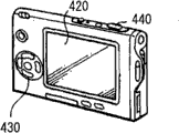
Figure 12 A and 12B show the outward appearance of the digital camera of the display unit 1 of having used previous embodiments etc.This digital camera for example has illuminating part 410, display part 420, menu switch 430 and the shutter release button 440 that is used to glisten.
The 3rd application examples
Figure 13 shows the outward appearance of the notebook computer of the display unit 1 of having used previous embodiments etc.This notebook computer for example has main body 510, be used to carry out character etc. input operation keyboard 520 and be used for the display part 530 of display image.
The 4th application examples
Figure 14 shows the outward appearance of the video camera of the display unit 1 of having used previous embodiments etc.This video camera for example has main body 610, be arranged on the leading flank of main body 610 and be used to take subject camera lens 620, take beginning/shutdown switch 630 and display part 640.
The 5th application examples
Figure 15 A to 15G shows the outward appearance of the mobile phone of the display unit 1 of having used previous embodiments etc.In this mobile phone, for example, upper body 710 and lower case 720 are bonded with each other by junction surface (hinge) 730.This mobile phone is provided with display 740, slave display 750, picture lamp 760 and camera 770.
Although with reference to aforesaid embodiment, embodiment and application examples the present invention has been described, has the invention is not restricted to aforesaid embodiment etc., and can carry out various improvement.
For example, in previous embodiments etc., the situation that first anode layer 41A is made of aluminium simple substance has been described.Yet,, comprise aluminium and can be used as first anode layer 41A as the alloy of main component if first anode layer 41A has the lower resistance than second plate layer 41C.
In addition, in aforesaid embodiment etc., the situation that the hole injection layer 51, hole transport layer 52, luminescent layer 53 and the electron transport layer 54 that constitute organic layer 50 formed by individual layer respectively mainly has been described, yet each layer can be formed also by multilayer.
In addition, the material of each layer, thickness, film build method, membrance casting condition etc. are not limited to those of in previous embodiments etc. explanation, also can adopt other material, thickness, film build method and membrance casting condition.
In addition, in aforesaid embodiment etc., top outgoing type organic electroluminescence device has been described, yet the present invention also can be applicable to bottom outgoing type organic electroluminescence device.In this case, substrate is made by transparent material, and anode, organic layer and negative electrode stack gradually on this transparency carrier according to the mode identical with previous embodiments.Yet, in this case, have as described above the illustrated such stepped construction of anode in the embodiment as the negative electrode of reflecting electrode, and anode is a transparency electrode.Particularly, in the negative electrode in this case, for example, second cathode layer (layer corresponding with second plate layer 41C) and first cathode layer (layer corresponding with first anode layer 41A) stack gradually from the organic layer side.Replacedly, first cathode layer (layer corresponding with first anode layer 41A) and second cathode layer (layer corresponding with second plate layer 41C) stack gradually from the organic layer side.In addition, as required, can between first cathode layer and second cathode layer, be formed with protective layer (intermediate layer).In having the bottom outgoing type organic electroluminescence device of said structure, the effect of resulting effect and previous embodiments is similar.
In addition, in aforesaid embodiment etc., the situation that three layers (red light luminescent layer, green luminescence layer and blue light-emittings) are used as the luminescent layer 53 of organic layer 50 that includes has been described; But the structure that is used to launch the luminescent layer of white light is not limited thereto.That is to say, can adopt the structure of two luminescent layers of two kinds of complementary colors, the combination of for example orange light luminescent layer and blue light-emitting, the combination of blue green light luminescent layer and red light luminescent layer, or the like.In addition, in aforesaid embodiment, the situation that three layers are gathered into folds on the thickness direction upper strata has been described.But each colour light emitting layer can be by forming with R, G and each pixel of each pixel of B spin coating accordingly independently.
In addition, in aforesaid embodiment etc., active matrix display device has been described.Yet the present invention can be applicable to the passive display unit.
One skilled in the art will appreciate that according to designing requirement and other factors, can in the scope of the appended claim of the present invention or its equivalent, carry out various modifications, combination, inferior combination and change.
Claims (16)
1. organic electroluminescence device, it comprises organic layer, and described organic layer is between anode and negative electrode, and described organic layer comprises luminescent layer,
Wherein, described anode has the stepped construction that comprises the ground floor and the second layer, described ground floor is by aluminium or comprise aluminium and constitute as the alloy of main component, and the described second layer is arranged between described ground floor and the described organic layer and by comprising the alloy of aluminium as main component and constitutes, and
The resistance of described ground floor is lower than the resistance of the described second layer.
2. organic electroluminescence device as claimed in claim 1, wherein said anode have the protective layer between the described ground floor and the described second layer.
3. organic electroluminescence device as claimed in claim 2, wherein said protective layer is made of molybdenum, titanium, chromium or nickel, perhaps constitutes by comprising the alloy of above-mentioned these elements as main component.
4. organic electroluminescence device as claimed in claim 1, the wherein said second layer have than higher thermal stability of the thermal stability of described ground floor and the protruding resistance higher than the protruding resistance of described ground floor.
5. organic electroluminescence device as claimed in claim 1, the auxiliary element of the alloy of the wherein said second layer comprise at least a element with work function littler than the work function of the main component of this alloy.
6. organic electroluminescence device as claimed in claim 5, the auxiliary element of the alloy of the wherein said second layer comprise at least a element in neodymium, tantalum, titanium, nickel, tungsten, the silicon.
7. organic electroluminescence device as claimed in claim 1, wherein said anode, described organic layer and described negative electrode upwards stack gradually, and
Described negative electrode is made by the material that has the light transmission of the light that sends from described luminescent layer.
8. organic electroluminescence device as claimed in claim 1, wherein, in the described organic layer with
The layer of described anode contact contains the compound shown in the following formula 1:
Formula 1

Here, R1~R6 represents hydrogen independently of one another, halogen, hydroxyl, amino, virtue is amino, replacement or unsubstituted carbonyl with 20 following carbon atoms, replacement or unsubstituted carbonyl ester group with 20 following carbon atoms, replacement or unsubstituted alkyl with 20 following carbon atoms, replacement or unsubstituted alkenyl with 20 following carbon atoms, replacement or unsubstituted alkoxyl with 20 following carbon atoms, replacement or unsubstituted aryl with 30 following carbon atoms, replacement or unsubstituted heterocyclic with 30 following carbon atoms, perhaps representative is selected from cyano group, nitro, isocyano group, the substituting group of one of silicyl; M is that 1~6 adjacent R m can mutually combine by circulus; And X1~X6 represents carbon atom or nitrogen-atoms independently of one another.
9. display unit, it includes organic electroluminescence devices, and described organic electroluminescence device comprises organic layer, and described organic layer is between anode and negative electrode, and described organic layer comprises luminescent layer,
Wherein, described anode has the stepped construction that comprises the ground floor and the second layer, described ground floor is by aluminium or comprise aluminium and constitute as the alloy of main component, and the described second layer is arranged between described ground floor and the described organic layer and by comprising the alloy of aluminium as main component and constitutes, and
The resistance of described ground floor is lower than the resistance of the described second layer.
10. display unit as claimed in claim 9, wherein said anode have the protective layer between the described ground floor and the described second layer.
11. display unit as claimed in claim 9, wherein said protective layer is made of molybdenum, titanium, chromium or nickel, perhaps constitutes by comprising the alloy of above-mentioned these elements as main component.
12. display unit as claimed in claim 9, the wherein said second layer have than higher thermal stability of the thermal stability of described ground floor and the protruding resistance higher than the protruding resistance of described ground floor.
13. display unit as claimed in claim 9, the auxiliary element of the alloy of the wherein said second layer comprise at least a element with work function littler than the work function of the main component of this alloy.
14. display unit as claimed in claim 9, the auxiliary element of the alloy of the wherein said second layer comprise at least a element in neodymium, tantalum, titanium, nickel, tungsten, the silicon.
15. display unit as claimed in claim 9, wherein said anode, described organic layer and described negative electrode upwards stack gradually, and
Described negative electrode is made by the material that has the light transmission of the light that sends from described luminescent layer.
16. display unit as claimed in claim 9, wherein, the layer that contacts with described anode in the described organic layer comprises the compound shown in the following formula 1:
Formula 1

Here, R1~R6 represents hydrogen independently of one another, halogen, hydroxyl, amino, virtue is amino, replacement or unsubstituted carbonyl with 20 following carbon atoms, replacement or unsubstituted carbonyl ester group with 20 following carbon atoms, replacement or unsubstituted alkyl with 20 following carbon atoms, replacement or unsubstituted alkenyl with 20 following carbon atoms, replacement or unsubstituted alkoxyl with 20 following carbon atoms, replacement or unsubstituted aryl with 30 following carbon atoms, replacement or unsubstituted heterocyclic with 30 following carbon atoms, perhaps representative is selected from cyano group, nitro, isocyano group, the substituting group of one of silicyl; M is that 1~6 adjacent R m can mutually combine by circulus; And X1~X6 represents carbon atom or nitrogen-atoms independently of one another.
Applications Claiming Priority (4)
| Application Number | Priority Date | Filing Date | Title |
|---|---|---|---|
| JP2009012180 | 2009-01-22 | ||
| JP2009-012180 | 2009-01-22 | ||
| JP2009-042084 | 2009-02-25 | ||
| JP2009042084A JP2010192413A (en) | 2009-01-22 | 2009-02-25 | Organic electroluminescence device, and display unit |
Publications (1)
| Publication Number | Publication Date |
|---|---|
| CN101789494A true CN101789494A (en) | 2010-07-28 |
Family
ID=42336386
Family Applications (1)
| Application Number | Title | Priority Date | Filing Date |
|---|---|---|---|
| CN201010001064A Pending CN101789494A (en) | 2009-01-22 | 2010-01-21 | Organic electroluminescence device and display unit |
Country Status (3)
| Country | Link |
|---|---|
| US (1) | US8524379B2 (en) |
| JP (1) | JP2010192413A (en) |
| CN (1) | CN101789494A (en) |
Cited By (6)
| Publication number | Priority date | Publication date | Assignee | Title |
|---|---|---|---|---|
| CN102738194A (en) * | 2011-04-01 | 2012-10-17 | 乐金显示有限公司 | Organic electroluminescent display device |
| CN107768545A (en) * | 2017-09-28 | 2018-03-06 | 上海天马微电子有限公司 | A kind of organic EL display panel and display device |
| CN107871825A (en) * | 2017-10-30 | 2018-04-03 | 周燕红 | A kind of organic luminescent device and preparation method |
| CN110611041A (en) * | 2019-08-21 | 2019-12-24 | 武汉华星光电半导体显示技术有限公司 | Display panel and display device thereof |
| CN113416190A (en) * | 2021-08-04 | 2021-09-21 | 华南理工大学 | Organic electroluminescent material based on pyrazolo [2,3-F ] [1,10] phenanthroline-2, 3-dinitrile and application thereof |
| CN114183724A (en) * | 2020-09-15 | 2022-03-15 | 株式会社小糸制作所 | Lamp unit and vehicle lamp |
Families Citing this family (15)
| Publication number | Priority date | Publication date | Assignee | Title |
|---|---|---|---|---|
| US20080139790A1 (en) * | 2006-12-08 | 2008-06-12 | Jennings Philip A | Chimeric antibodies |
| JP5969216B2 (en) | 2011-02-11 | 2016-08-17 | 株式会社半導体エネルギー研究所 | Light emitting element, display device, lighting device, and manufacturing method thereof |
| JP2012243742A (en) * | 2011-05-24 | 2012-12-10 | Kobe Steel Ltd | Wiring structure including organic el display reflective anode electrode |
| JP2012243740A (en) * | 2011-05-24 | 2012-12-10 | Kobe Steel Ltd | Wiring structure including organic el display reflective anode electrode |
| JP6023404B2 (en) * | 2011-05-24 | 2016-11-09 | 株式会社神戸製鋼所 | Manufacturing method of wiring structure including reflective anode electrode for organic EL display |
| KR20130143671A (en) * | 2011-05-24 | 2013-12-31 | 가부시키가이샤 고베 세이코쇼 | Wiring structure comprising reflective anode electrode for organic el displays |
| KR101284736B1 (en) * | 2012-01-25 | 2013-07-17 | 한국전자통신연구원 | Light source apparatus |
| JP6111455B2 (en) * | 2012-03-12 | 2017-04-12 | 株式会社Joled | Display panel, display device and electronic device |
| JP5906159B2 (en) * | 2012-09-13 | 2016-04-20 | 株式会社神戸製鋼所 | Al alloy film for anode electrode of organic EL element, organic EL element, and Al alloy sputtering target |
| RU2015145444A (en) | 2013-05-03 | 2017-06-07 | Магна Интернэшнэл Инк. | ALUMINUM SPOT WELDING METHOD |
| JP6211873B2 (en) * | 2013-09-30 | 2017-10-11 | 株式会社ジャパンディスプレイ | Organic EL display device and method of manufacturing organic EL display device |
| KR102136789B1 (en) * | 2014-06-17 | 2020-07-23 | 삼성디스플레이 주식회사 | Organic light emitting diode |
| JP2018032601A (en) * | 2016-08-26 | 2018-03-01 | 株式会社神戸製鋼所 | REFLECTION ELECTRODE AND Al ALLOY SPUTTERING TARGET |
| US11309512B2 (en) | 2017-03-30 | 2022-04-19 | Sharp Kabushiki Kaisha | Organic EL display device and method for manufacturing organic EL display device |
| CN110931650A (en) * | 2019-11-22 | 2020-03-27 | 深圳市华星光电半导体显示技术有限公司 | Organic light-emitting diode device, display panel and preparation method of display panel |
Citations (4)
| Publication number | Priority date | Publication date | Assignee | Title |
|---|---|---|---|---|
| CN1607876A (en) * | 2003-09-19 | 2005-04-20 | 索尼株式会社 | Organic light emitting device, manufacturing method thereof, and display unit |
| CN1747615A (en) * | 2004-09-07 | 2006-03-15 | 索尼株式会社 | Organic electroluminescent device and display device |
| CN1934727A (en) * | 2004-03-19 | 2007-03-21 | 伊斯曼柯达公司 | Organic light-emitting device having improved stability |
| JP2008226494A (en) * | 2007-03-08 | 2008-09-25 | Mt Picture Display Co Ltd | Electrode and display device |
Family Cites Families (9)
| Publication number | Priority date | Publication date | Assignee | Title |
|---|---|---|---|---|
| US6501217B2 (en) * | 1998-02-02 | 2002-12-31 | International Business Machines Corporation | Anode modification for organic light emitting diodes |
| US7560175B2 (en) * | 1999-12-31 | 2009-07-14 | Lg Chem, Ltd. | Electroluminescent devices with low work function anode |
| JP3804858B2 (en) | 2001-08-31 | 2006-08-02 | ソニー株式会社 | Organic electroluminescent device and manufacturing method thereof |
| JP2003234193A (en) | 2002-02-07 | 2003-08-22 | Canon Inc | Organic light emitting element and its manufacturing method, and base material having positive electrode of organic light emitting element |
| US6917158B2 (en) * | 2002-03-08 | 2005-07-12 | City University Of Hong Kong | High-qualty aluminum-doped zinc oxide layer as transparent conductive electrode for organic light-emitting devices |
| KR100527193B1 (en) * | 2003-06-03 | 2005-11-08 | 삼성에스디아이 주식회사 | organic electroluminescence device employing multi-layered pixel electrode and method of fabricating the same |
| KR100546662B1 (en) * | 2003-08-05 | 2006-01-26 | 엘지전자 주식회사 | Organic electroluminescence device |
| US6963081B2 (en) * | 2003-09-30 | 2005-11-08 | Osram Otpo Semiconductors Gmbh | Interfacial trap layer to improve carrier injection |
| JP4823685B2 (en) * | 2005-12-28 | 2011-11-24 | 京セラ株式会社 | EL device and manufacturing method thereof |
-
2009
- 2009-02-25 JP JP2009042084A patent/JP2010192413A/en active Pending
-
2010
- 2010-01-15 US US12/688,052 patent/US8524379B2/en not_active Expired - Fee Related
- 2010-01-21 CN CN201010001064A patent/CN101789494A/en active Pending
Patent Citations (4)
| Publication number | Priority date | Publication date | Assignee | Title |
|---|---|---|---|---|
| CN1607876A (en) * | 2003-09-19 | 2005-04-20 | 索尼株式会社 | Organic light emitting device, manufacturing method thereof, and display unit |
| CN1934727A (en) * | 2004-03-19 | 2007-03-21 | 伊斯曼柯达公司 | Organic light-emitting device having improved stability |
| CN1747615A (en) * | 2004-09-07 | 2006-03-15 | 索尼株式会社 | Organic electroluminescent device and display device |
| JP2008226494A (en) * | 2007-03-08 | 2008-09-25 | Mt Picture Display Co Ltd | Electrode and display device |
Cited By (8)
| Publication number | Priority date | Publication date | Assignee | Title |
|---|---|---|---|---|
| CN102738194A (en) * | 2011-04-01 | 2012-10-17 | 乐金显示有限公司 | Organic electroluminescent display device |
| CN102738194B (en) * | 2011-04-01 | 2015-07-08 | 乐金显示有限公司 | Organic electroluminescent display device |
| CN107768545A (en) * | 2017-09-28 | 2018-03-06 | 上海天马微电子有限公司 | A kind of organic EL display panel and display device |
| CN107768545B (en) * | 2017-09-28 | 2020-09-11 | 上海天马微电子有限公司 | Organic electroluminescent display panel and display device |
| CN107871825A (en) * | 2017-10-30 | 2018-04-03 | 周燕红 | A kind of organic luminescent device and preparation method |
| CN110611041A (en) * | 2019-08-21 | 2019-12-24 | 武汉华星光电半导体显示技术有限公司 | Display panel and display device thereof |
| CN114183724A (en) * | 2020-09-15 | 2022-03-15 | 株式会社小糸制作所 | Lamp unit and vehicle lamp |
| CN113416190A (en) * | 2021-08-04 | 2021-09-21 | 华南理工大学 | Organic electroluminescent material based on pyrazolo [2,3-F ] [1,10] phenanthroline-2, 3-dinitrile and application thereof |
Also Published As
| Publication number | Publication date |
|---|---|
| US20100181904A1 (en) | 2010-07-22 |
| JP2010192413A (en) | 2010-09-02 |
| US8524379B2 (en) | 2013-09-03 |
Similar Documents
| Publication | Publication Date | Title |
|---|---|---|
| CN101789494A (en) | Organic electroluminescence device and display unit | |
| US7053545B2 (en) | Light-emitting device and method of manufacturing the same | |
| CN101997086B (en) | Light emitting device | |
| CN101013745B (en) | Display device and display unit | |
| CN101308865B (en) | Organic electroluminescence display device | |
| CN101931057B (en) | Organic electroluminescence device, method of manufacturing an organic electroluminescence device and display unit including the same | |
| CN101388438B (en) | Organic electroluminescent device, fabrication process of organic electroluminescent device, display device, and fabrication process of display device | |
| US8829497B2 (en) | Display element, display device, and electronic apparatus | |
| US20100051990A1 (en) | Electroluminescence Device | |
| CN102738406A (en) | Organic light emitting device and display unit including the same | |
| WO2012090786A1 (en) | Light-emitting device, display device, and illumination device | |
| US7911128B2 (en) | Organic electroluminescence display device having anode and drain sealing structure and a method for fabricating thereof | |
| EP2487671A1 (en) | Light emitting panel device wherein a plurality of panels respectively having light emitting sections are connected , and image display device and illuminating device provided with the light emitting panel device | |
| CN101859794B (en) | Display and method of manufacturing the same | |
| CN100524890C (en) | Organic electroluminescent element, panel display and portable electronic device | |
| CN103000655A (en) | Display and electronic unit | |
| CN103367650A (en) | Light emitting element and display apparatus | |
| JP2012238544A (en) | Display element, display device, and electronic apparatus | |
| JP2009259509A (en) | Organic electroluminescence apparatus | |
| KR102317062B1 (en) | Very high resolution stacked oled display | |
| CN110233163A (en) | Display device, its manufacturing method and the method for manufacturing electronic equipment | |
| KR20150040249A (en) | Light emitting device, display unit including the same, and electronic apparatus | |
| CN101257035A (en) | Organic electroluminescence display device with top luminous | |
| CN101147274B (en) | Light-emitting element, light-emitting device, and electrical appliance using light-emitting element | |
| US10840472B2 (en) | Display device and light emitting device |
Legal Events
| Date | Code | Title | Description |
|---|---|---|---|
| C06 | Publication | ||
| PB01 | Publication | ||
| C10 | Entry into substantive examination | ||
| SE01 | Entry into force of request for substantive examination | ||
| C12 | Rejection of a patent application after its publication | ||
| RJ01 | Rejection of invention patent application after publication |
Application publication date: 20100728 |