JP2009016841A - Housing with electrical module - Google Patents
Housing with electrical module Download PDFInfo
- Publication number
- JP2009016841A JP2009016841A JP2008174456A JP2008174456A JP2009016841A JP 2009016841 A JP2009016841 A JP 2009016841A JP 2008174456 A JP2008174456 A JP 2008174456A JP 2008174456 A JP2008174456 A JP 2008174456A JP 2009016841 A JP2009016841 A JP 2009016841A
- Authority
- JP
- Japan
- Prior art keywords
- contact means
- module
- housing
- electrical
- outer housing
- Prior art date
- Legal status (The legal status is an assumption and is not a legal conclusion. Google has not performed a legal analysis and makes no representation as to the accuracy of the status listed.)
- Pending
Links
- 238000005219 brazing Methods 0.000 claims description 4
- 239000000853 adhesive Substances 0.000 claims description 3
- 230000001070 adhesive effect Effects 0.000 claims description 3
- 238000000465 moulding Methods 0.000 claims description 3
- 238000003466 welding Methods 0.000 claims description 3
- 150000001875 compounds Chemical class 0.000 claims description 2
- 238000003825 pressing Methods 0.000 claims description 2
- 238000007789 sealing Methods 0.000 claims description 2
- 239000002184 metal Substances 0.000 description 9
- 239000000758 substrate Substances 0.000 description 7
- 238000011156 evaluation Methods 0.000 description 6
- 230000002093 peripheral effect Effects 0.000 description 4
- 230000001133 acceleration Effects 0.000 description 2
- 238000005266 casting Methods 0.000 description 2
- 239000000470 constituent Substances 0.000 description 2
- 238000005516 engineering process Methods 0.000 description 2
- 238000000034 method Methods 0.000 description 2
- 239000003990 capacitor Substances 0.000 description 1
- 239000000919 ceramic Substances 0.000 description 1
- 239000003985 ceramic capacitor Substances 0.000 description 1
- 239000004020 conductor Substances 0.000 description 1
- 230000005672 electromagnetic field Effects 0.000 description 1
- 230000007613 environmental effect Effects 0.000 description 1
- 239000000463 material Substances 0.000 description 1
Images

Classifications
-
- H—ELECTRICITY
- H05—ELECTRIC TECHNIQUES NOT OTHERWISE PROVIDED FOR
- H05K—PRINTED CIRCUITS; CASINGS OR CONSTRUCTIONAL DETAILS OF ELECTRIC APPARATUS; MANUFACTURE OF ASSEMBLAGES OF ELECTRICAL COMPONENTS
- H05K5/00—Casings, cabinets or drawers for electric apparatus
- H05K5/0026—Casings, cabinets or drawers for electric apparatus provided with connectors and printed circuit boards [PCB], e.g. automotive electronic control units
- H05K5/0078—Casings, cabinets or drawers for electric apparatus provided with connectors and printed circuit boards [PCB], e.g. automotive electronic control units specially adapted for acceleration sensors, e.g. crash sensors, airbag sensors
-
- H—ELECTRICITY
- H01—ELECTRIC ELEMENTS
- H01L—SEMICONDUCTOR DEVICES NOT COVERED BY CLASS H10
- H01L2924/00—Indexing scheme for arrangements or methods for connecting or disconnecting semiconductor or solid-state bodies as covered by H01L24/00
- H01L2924/15—Details of package parts other than the semiconductor or other solid state devices to be connected
- H01L2924/181—Encapsulation
Abstract
Description
本発明は、電機部品を備えたモジュールであって、電機部品を取り囲んでいる内部ハウジングが設けられていて、該内部ハウジングが、少なくとも1つの外側に第1の電気コンタクト手段を有しており、内部ハウジングが内部に配置されている外側ハウジングが設けられており、外側ハウジングが第2の電気コンタクト手段を有しており、第2の電気コンタクト手段が外側ハウジングの内部から少なくとも1つの外側にまで延びている形式のものに関する。 The present invention is a module including an electrical component, wherein an internal housing surrounding the electrical component is provided, and the internal housing has first electrical contact means on at least one outer side, An outer housing is provided with an inner housing disposed therein, the outer housing having second electrical contact means, the second electrical contact means extending from the inside of the outer housing to at least one outside. It relates to the extended form.
従来技術では、マイクロメカニカルセンサが、プラスチック製のチップハウジング内に金属製又は有機の基板(リードフレーム、積層板)と共にセンサエレメントとしてパッケージされている。周辺センサとして使用するため、特に自動車における周辺加速度センサのためには、センサエレメントは、外側ハウジング内において中間坦体としてのプリント基板に取り付けられる。 In the prior art, a micromechanical sensor is packaged as a sensor element together with a metal or organic substrate (lead frame, laminate) in a plastic chip housing. For use as a peripheral sensor, in particular for peripheral acceleration sensors in motor vehicles, the sensor element is mounted on a printed circuit board as an intermediate carrier in the outer housing.
本発明の課題は、冒頭に述べた形式の、電機部品を備えたモジュールを改良して、簡単に、小型にかつ安価に製造することができるモジュールを提供することである。 An object of the present invention is to provide a module that can be manufactured easily, in a small size, and at low cost by improving a module having an electrical component of the type described at the beginning.
この課題を解決するために本発明の構成では、電機部品を備えたモジュールであって、
電機部品を取り囲んでいる内部ハウジングが設けられていて、該内部ハウジングが、少なくとも1つの外側に第1の電気コンタクト手段を有しており、内部ハウジングが内部に配置されている外側ハウジングが設けられており、外側ハウジングが第2の電気コンタクト手段を有しており、この第2の電気コンタクト手段が外側ハウジングの内部から少なくとも1つの外側にまで延びている形式のものにおいて、第1のコンタクト手段と第2のコンタクト手段とが互いに接続されており、つまり両コンタクト手段の間にプリント基板が配置されていない。
In order to solve this problem, in the configuration of the present invention, a module including electrical parts,
An inner housing is provided surrounding the electrical component, the inner housing having at least one outer first electrical contact means, and an outer housing having the inner housing disposed therein. Wherein the outer housing has second electrical contact means, the second electrical contact means extending from the inside of the outer housing to at least one outside. And the second contact means are connected to each other, that is, no printed circuit board is disposed between the contact means.
このように構成されていることによって、本発明によるモジュールは、簡単に、小型にかつ安価に製造することができる。 With this configuration, the module according to the present invention can be easily manufactured in a small size and at a low cost.
本発明の有利な構成では、第1のコンタクト手段と第2のコンタクト手段とが少なくとも1つの領域において互いに向かい合って位置するように配置されていて、電機部品がこの領域において第1のコンタクト手段と第2のコンタクト手段との間に配置されている。このように構成されていると、電機部品のための電磁遮蔽体が有利に得られる。本発明の別の有利な構成では、第1のコンタクト手段と第2のコンタクト手段とが、溶接結合、ろう接結合、プレス結合又はワイヤボンディング結合によって互いに接続されている。また、内側ハウジングが外側ハウジング内に、接着結合又は封止用コンパウンドを用いて又は包埋成形に基づいて固定されていると、有利である。本発明の特に有利な構成では、モジュールがセンサモジュールであって、電機部品がセンサ、特にマイクロメカニカルセンサである。さらにまた、センサモジュール内に、電機部品の他に、従来技術においてプリント基板に配置されている別の構成エレメントが組み込まれているような構成も有利である。 In an advantageous configuration of the invention, the first contact means and the second contact means are arranged to face each other in at least one region, and the electrical component is arranged in this region with the first contact means. It arrange | positions between 2nd contact means. If comprised in this way, the electromagnetic shielding body for electrical components will be obtained advantageously. In another advantageous configuration of the invention, the first contact means and the second contact means are connected to each other by welding, brazing, pressing or wire bonding. It is also advantageous if the inner housing is fixed in the outer housing using an adhesive bond or sealing compound or based on embedding molding. In a particularly advantageous configuration of the invention, the module is a sensor module and the electrical component is a sensor, in particular a micromechanical sensor. Furthermore, a configuration in which another constituent element arranged on the printed circuit board in the prior art is incorporated in addition to the electrical component in the sensor module is also advantageous.
有利には、マイクロメカニカルセンサエレメントを備えたセンサにおいて、センサモジュールハウジングが付加的なプリント基板なしに直接外側ハウジングに取り付けられている。構成エレメントの適宜な配置によって、センサエレメント及び電子評価回路を、障害電磁場及び環境からの影響に対して良好に保護することができる。付加的に、付加的に必要なパッシブ型の電機部品、例えばセラミック製のチップコンデンサがモジュールハウジングに組み込まれる。本発明による構造は一連の利点をもたらす。センサはプリント基板(Leiterplatte)又はその他の坦体(Unterlage)もしくはその他の基板(Substrat)なしに特に安価に製造することができる。センサの構造寸法は小さくすることができる。プリント基板にセンサモジュールを固定及び接触接続のための、例えばSMD装着、ろう接のような組立てステップ及びプロセスは不要になる。また、外側ハウジングにおけるプリント基板の、例えばプレス嵌めのような固定及び接触接続の組立てステップも省くことができる。これによってコスト節減と品質改善が可能になる。外側ハウジングを閉鎖するために、本発明によるモジュールでは、汎用のプリント基板技術とは両立し得ない技術を使用することができ、又は内部ハウジングと外部ハウジングとの注型又はダイレクト包埋成形において見られるような、品質の劣化が生ぜしめられることもない。 Advantageously, in sensors with micromechanical sensor elements, the sensor module housing is directly attached to the outer housing without an additional printed circuit board. With appropriate arrangement of the constituent elements, the sensor element and the electronic evaluation circuit can be well protected against disturbance electromagnetic fields and environmental influences. In addition, additionally required passive type electric parts, for example, a ceramic chip capacitor, are incorporated in the module housing. The structure according to the invention provides a series of advantages. The sensor can be produced particularly inexpensively without a printed circuit board (Leiterplatte) or other carrier (Unterlage) or other substrate (Substrat). The structural dimensions of the sensor can be reduced. For example, assembly steps and processes such as SMD mounting and brazing are not required for fixing the sensor module to the printed circuit board and for contact connection. In addition, the assembly step of fixing and contact connection, such as a press fit, of the printed circuit board in the outer housing can be omitted. This allows cost savings and quality improvements. To close the outer housing, the module according to the invention can use techniques that are incompatible with general-purpose printed circuit board technology, or see in casting or direct embedding of the inner and outer housings. As a result, the quality is not degraded.
次に図面を参照しながら本発明の有利な実施形態を説明する。 An advantageous embodiment of the invention will now be described with reference to the drawings.
図1には、従来技術の電気部品を備えたモジュールが示されている。従来技術は、金属製基板又は有機基板(リードフレーム、積層板)を備えたプラスチック製の、センサエレメントとしてのチップハウジング1内におけるマイクロメカニカルセンサ3のパッケージである。周辺センサとしての使用のために、例えば自動車における周辺加速度センサのために、センサエレメントは、外側ハウジング5内において中間坦体としてのプリント基板4に取り付けられる。付加的に、プリント基板4には別の受動型電機部品が、多くの場合セラミック製のコンデンサが設けられている。EMV保護としてモジュールはしばしば次のように、すなわちセンサチップ3又は評価回路3が、チップハウジング1に内蔵された坦体ストリップ(リードフレーム)2と金属面例えばアース面との間においてプリント基板4上に位置するように、プリント基板4に配置されている。これによって金属製の遮蔽体が得られる。プリント基板4は外側ハウジング5内において、コンタクトピン6に取り付けられており、これらのコンタクトピン6は外側ハウジング5の内部から外側に達し、外方への電気的な接触接続の可能性を示している。
FIG. 1 shows a module with prior art electrical components. The prior art is a package of a
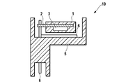
図2には、電機部品を備えた本発明によるモジュールが示されている。評価回路を備えたマイクロメカニカルセンサチップ3とリードフレーム2とから成るセンサエレメント1は、外側ハウジング5内に組み込まれている。金属製のリードフレームの代わりに、モジュールは、金属製の導体路を備えた坦体基板として積層板を有することもできる(LGA)。センサモジュールの接触接続のために、金属製のコンタクトピン6が外側ハウジング5に設けられている。これらのコンタクトピン6は、そのうちの1つのコンタクトピン6の一部が、面状にセンサエレメント1の下に配置されているように、構成されており、その結果センサチップ及び評価回路3は、モジュールハウジング1の金属製のリードフレーム2とコンタクトピン6の面状に形成された部分との間に位置する。これによってセンサチップ及び評価回路3の良好な金属遮蔽が得られる。
FIG. 2 shows a module according to the invention with electrical components. A sensor element 1 including a
センサエレメント1は、適宜な材料を用いた包埋成形、注型又は接着によって、外側ハウジング5内に固定されている。センサモジュールの電気接続部は、コンタクトピンと導電接続されており、この場合導電接続としては例えば、溶接、ろう接又はワイヤボンディング、冷間の接触接続技術(例えばプレス成形)又は、異方性又は等方性の導電接着剤が挙げられる。 The sensor element 1 is fixed in the outer housing 5 by embedding using an appropriate material, casting or adhesion. The electrical connection part of the sensor module is conductively connected to the contact pin. In this case, examples of the conductive connection include welding, brazing or wire bonding, cold contact connection technology (for example, press molding), anisotropic or the like. An anisotropic conductive adhesive is mentioned.
センサエレメント1の運転のために必要な付加的なアクティブ又はパッシブな構成エレメントは、センサエレメント1に、又はセンサエレメント1に内蔵された評価回路3に組み込まれることができる。従来技術におけるような付加的な基板4(プリント基板)は不要である。
Additional active or passive components required for the operation of the sensor element 1 can be incorporated in the sensor element 1 or in an
本発明はセンサモジュールに制限されるものではない。図2に示された一般化された実施例では、電機部品3を備えたモジュール10が示されており、このモジュール10の内側ハウジング1は、電機部品3を少なくとも部分的に取り囲んでいて、少なくとも外側に第1の電気コンタクト手段2を有しており、この第1の電気コンタクト手段2は、電機部品3を電気的に接触接続可能にする。モジュール10はさらに外側ハウジング5を有しており、この外側ハウジング5の内部には内側ハウジング1が配置されている。この場合外側ハウジング5は第2の電気コンタクト手段6を有しており、この第2の電気コンタクト手段6は、外側ハウジング5の内部から外側ハウジング5の少なくとも1つの外側にまで延びている。本発明によれば第1のコンタクト手段2と第2のコンタクト手段6とは互いに接続されている。この接続は直接行われており、つまり両コンタクト手段2,6の間には、図1に示されているようなプリント基板4は設けられておらず、またその他の基板も配置されていない。第1のコンタクト手段2と第2のコンタクト手段6とは、図示されているように少なくとも一部の領域において、互いに向かい合って位置するように配置されており、電機部品3はこの領域において第1のコンタクト手段2と第2のコンタクト手段6との間に配置されていて、これにより第1のコンタクト手段2と第2のコンタクト手段6とは電機部品3のための電磁遮蔽体を形成している。
The present invention is not limited to the sensor module. In the generalized embodiment shown in FIG. 2, a
1 チップハウジング(内側ハウジング)、 2 坦体ストリップ(リードフレーム)、 3 センサチップ(電機部品)、 4 プリント基板、 5 外側ハウジング、 6 コンタクトピン、 10 モジュール 1 chip housing (inner housing), 2 carrier strip (lead frame), 3 sensor chip (electrical parts), 4 printed circuit board, 5 outer housing, 6 contact pin, 10 module
Claims (5)
電機部品(3)を取り囲んでいる内部ハウジング(1)が設けられていて、該内部ハウジング(1)が、少なくとも1つの外側に第1の電気コンタクト手段(2)を有しており、
内部ハウジング(1)が内部に配置されている外側ハウジング(5)が設けられており、
外側ハウジング(5)が第2の電気コンタクト手段(6)を有しており、
第2の電気コンタクト手段(6)が外側ハウジング(5)の内部から少なくとも1つの外側にまで延びている形式のものにおいて、
第1のコンタクト手段(2)と第2のコンタクト手段(6)とが互いに接続されていることを特徴とする、電機部品(3)を備えたモジュール(10)。 A module (10) comprising an electrical component (3),
An inner housing (1) surrounding the electrical component (3) is provided, the inner housing (1) having at least one outer first electrical contact means (2);
An outer housing (5) is provided in which an inner housing (1) is arranged;
The outer housing (5) has second electrical contact means (6);
In the form in which the second electrical contact means (6) extends from the inside of the outer housing (5) to at least one outside,
A module (10) comprising an electrical component (3), characterized in that the first contact means (2) and the second contact means (6) are connected to each other.
Applications Claiming Priority (1)
| Application Number | Priority Date | Filing Date | Title |
|---|---|---|---|
| DE102007031562.9A DE102007031562B4 (en) | 2007-07-06 | 2007-07-06 | Housing with an electrical module |
Publications (2)
| Publication Number | Publication Date |
|---|---|
| JP2009016841A true JP2009016841A (en) | 2009-01-22 |
| JP2009016841A5 JP2009016841A5 (en) | 2011-08-04 |
Family
ID=40092510
Family Applications (1)
| Application Number | Title | Priority Date | Filing Date |
|---|---|---|---|
| JP2008174456A Pending JP2009016841A (en) | 2007-07-06 | 2008-07-03 | Housing with electrical module |
Country Status (5)
| Country | Link |
|---|---|
| US (1) | US7791891B2 (en) |
| JP (1) | JP2009016841A (en) |
| DE (1) | DE102007031562B4 (en) |
| FR (1) | FR2918503B1 (en) |
| IT (1) | IT1390818B1 (en) |
Families Citing this family (4)
| Publication number | Priority date | Publication date | Assignee | Title |
|---|---|---|---|---|
| DE102010039063B4 (en) | 2010-08-09 | 2024-01-18 | Robert Bosch Gmbh | Sensor module with an electromagnetically shielded electrical component and method for producing such a sensor module |
| DE102011081016A1 (en) * | 2011-08-16 | 2013-02-21 | Robert Bosch Gmbh | Sensor module and method for producing a sensor module |
| DE102013226236A1 (en) * | 2013-12-17 | 2015-06-18 | Robert Bosch Gmbh | Electrical assembly |
| US10804913B1 (en) | 2018-09-10 | 2020-10-13 | Inphi Corporation | Clock and data recovery devices with fractional-N PLL |
Citations (2)
| Publication number | Priority date | Publication date | Assignee | Title |
|---|---|---|---|---|
| JPH0278298A (en) * | 1988-09-14 | 1990-03-19 | Hitachi Ltd | Electronic device |
| JPH07288332A (en) * | 1994-02-25 | 1995-10-31 | Fujitsu Ltd | Light element assembly and manufacture thereof |
Family Cites Families (8)
| Publication number | Priority date | Publication date | Assignee | Title |
|---|---|---|---|---|
| JP3540471B2 (en) | 1995-11-30 | 2004-07-07 | 三菱電機株式会社 | Semiconductor module |
| US5948991A (en) | 1996-12-09 | 1999-09-07 | Denso Corporation | Semiconductor physical quantity sensor device having semiconductor sensor chip integrated with semiconductor circuit chip |
| JP3452835B2 (en) * | 1999-05-28 | 2003-10-06 | 三菱電機株式会社 | Pressure sensor device |
| DE10052406A1 (en) * | 2000-10-20 | 2002-05-23 | Bosch Gmbh Robert | Pressure sensor module |
| DE10054013B4 (en) * | 2000-11-01 | 2007-06-21 | Robert Bosch Gmbh | Pressure sensor module |
| DE10065013B4 (en) * | 2000-12-23 | 2009-12-24 | Robert Bosch Gmbh | Method for producing a micromechanical component |
| JP4892781B2 (en) | 2001-01-18 | 2012-03-07 | 富士電機株式会社 | Semiconductor physical quantity sensor |
| DE10213648B4 (en) | 2002-03-27 | 2011-12-15 | Semikron Elektronik Gmbh & Co. Kg | The power semiconductor module |
-
2007
- 2007-07-06 DE DE102007031562.9A patent/DE102007031562B4/en active Active
-
2008
- 2008-07-01 IT ITMI2008A001215A patent/IT1390818B1/en active
- 2008-07-02 FR FR0854468A patent/FR2918503B1/en active Active
- 2008-07-02 US US12/217,301 patent/US7791891B2/en active Active
- 2008-07-03 JP JP2008174456A patent/JP2009016841A/en active Pending
Patent Citations (2)
| Publication number | Priority date | Publication date | Assignee | Title |
|---|---|---|---|---|
| JPH0278298A (en) * | 1988-09-14 | 1990-03-19 | Hitachi Ltd | Electronic device |
| JPH07288332A (en) * | 1994-02-25 | 1995-10-31 | Fujitsu Ltd | Light element assembly and manufacture thereof |
Also Published As
| Publication number | Publication date |
|---|---|
| DE102007031562A1 (en) | 2009-01-08 |
| FR2918503B1 (en) | 2013-04-05 |
| ITMI20081215A1 (en) | 2009-01-07 |
| US20090027861A1 (en) | 2009-01-29 |
| DE102007031562B4 (en) | 2024-01-18 |
| IT1390818B1 (en) | 2011-10-19 |
| US7791891B2 (en) | 2010-09-07 |
| FR2918503A1 (en) | 2009-01-09 |
Similar Documents
| Publication | Publication Date | Title |
|---|---|---|
| JP5453310B2 (en) | Pressure sensor module | |
| US20090072360A1 (en) | Molded semiconductor device including IC-chip covered with conductor member | |
| US8174097B2 (en) | Electric sub-assembly | |
| US10964623B2 (en) | Electronic module and method for encapsulation thereof | |
| JP2010509742A (en) | Standardized electronic casing with modular contact partner | |
| JP2009016841A (en) | Housing with electrical module | |
| US9645163B2 (en) | Sensor with a single electrical carrier means | |
| JP6277061B2 (en) | Electronic control unit | |
| US20130010442A1 (en) | Circuit arrangement and associated controller for a motor vehicle | |
| JP5939895B2 (en) | In-vehicle electronic control unit | |
| US8094465B2 (en) | Module and method for producing a module | |
| US8174834B2 (en) | Molded housing used in force fit method | |
| US20130069427A1 (en) | Circuit arrangement and associated controller for a motor vehicle | |
| JP2009016841A5 (en) | ||
| WO2014208080A1 (en) | Electronic apparatus | |
| JP4513758B2 (en) | Mold package and manufacturing method thereof | |
| KR20170140233A (en) | Electronic modules for transmission control devices | |
| JP2012129306A (en) | Electronic apparatus | |
| JP5392243B2 (en) | Electronic device and manufacturing method thereof | |
| US20170354036A1 (en) | Electronic Assembly and Method for the Production thereof | |
| JP2012129305A (en) | Electronic apparatus | |
| JP2005093905A (en) | Electronic substrate unit | |
| JP6149982B2 (en) | Electronic equipment | |
| JP5720450B2 (en) | Pressure sensor and pressure sensor mounting structure | |
| JP2009278026A (en) | Electronic component mounting structure and on-vehicle sensor |
Legal Events
| Date | Code | Title | Description |
|---|---|---|---|
| RD04 | Notification of resignation of power of attorney |
Free format text: JAPANESE INTERMEDIATE CODE: A7424 Effective date: 20101227 |
|
| A521 | Request for written amendment filed |
Free format text: JAPANESE INTERMEDIATE CODE: A523 Effective date: 20110616 |
|
| A621 | Written request for application examination |
Free format text: JAPANESE INTERMEDIATE CODE: A621 Effective date: 20110616 |
|
| A131 | Notification of reasons for refusal |
Free format text: JAPANESE INTERMEDIATE CODE: A131 Effective date: 20121005 |
|
| A601 | Written request for extension of time |
Free format text: JAPANESE INTERMEDIATE CODE: A601 Effective date: 20121227 |
|
| A02 | Decision of refusal |
Free format text: JAPANESE INTERMEDIATE CODE: A02 Effective date: 20130603 |