JP2008503034A - LED array system - Google Patents
LED array system Download PDFInfo
- Publication number
- JP2008503034A JP2008503034A JP2007515209A JP2007515209A JP2008503034A JP 2008503034 A JP2008503034 A JP 2008503034A JP 2007515209 A JP2007515209 A JP 2007515209A JP 2007515209 A JP2007515209 A JP 2007515209A JP 2008503034 A JP2008503034 A JP 2008503034A
- Authority
- JP
- Japan
- Prior art keywords
- light
- assembly
- led
- optical sheet
- sheet
- Prior art date
- Legal status (The legal status is an assumption and is not a legal conclusion. Google has not performed a legal analysis and makes no representation as to the accuracy of the status listed.)
- Pending
Links
Images


Classifications
-
- G—PHYSICS
- G02—OPTICS
- G02B—OPTICAL ELEMENTS, SYSTEMS OR APPARATUS
- G02B6/00—Light guides; Structural details of arrangements comprising light guides and other optical elements, e.g. couplings
- G02B6/0001—Light guides; Structural details of arrangements comprising light guides and other optical elements, e.g. couplings specially adapted for lighting devices or systems
- G02B6/0011—Light guides; Structural details of arrangements comprising light guides and other optical elements, e.g. couplings specially adapted for lighting devices or systems the light guides being planar or of plate-like form
- G02B6/0066—Light guides; Structural details of arrangements comprising light guides and other optical elements, e.g. couplings specially adapted for lighting devices or systems the light guides being planar or of plate-like form characterised by the light source being coupled to the light guide
- G02B6/0068—Arrangements of plural sources, e.g. multi-colour light sources
-
- G—PHYSICS
- G02—OPTICS
- G02B—OPTICAL ELEMENTS, SYSTEMS OR APPARATUS
- G02B3/00—Simple or compound lenses
- G02B3/0006—Arrays
- G02B3/0037—Arrays characterized by the distribution or form of lenses
- G02B3/0056—Arrays characterized by the distribution or form of lenses arranged along two different directions in a plane, e.g. honeycomb arrangement of lenses
-
- G—PHYSICS
- G02—OPTICS
- G02B—OPTICAL ELEMENTS, SYSTEMS OR APPARATUS
- G02B6/00—Light guides; Structural details of arrangements comprising light guides and other optical elements, e.g. couplings
- G02B6/0001—Light guides; Structural details of arrangements comprising light guides and other optical elements, e.g. couplings specially adapted for lighting devices or systems
- G02B6/0011—Light guides; Structural details of arrangements comprising light guides and other optical elements, e.g. couplings specially adapted for lighting devices or systems the light guides being planar or of plate-like form
- G02B6/0033—Means for improving the coupling-out of light from the light guide
- G02B6/005—Means for improving the coupling-out of light from the light guide provided by one optical element, or plurality thereof, placed on the light output side of the light guide
- G02B6/0055—Reflecting element, sheet or layer
-
- G—PHYSICS
- G02—OPTICS
- G02F—OPTICAL DEVICES OR ARRANGEMENTS FOR THE CONTROL OF LIGHT BY MODIFICATION OF THE OPTICAL PROPERTIES OF THE MEDIA OF THE ELEMENTS INVOLVED THEREIN; NON-LINEAR OPTICS; FREQUENCY-CHANGING OF LIGHT; OPTICAL LOGIC ELEMENTS; OPTICAL ANALOGUE/DIGITAL CONVERTERS
- G02F1/00—Devices or arrangements for the control of the intensity, colour, phase, polarisation or direction of light arriving from an independent light source, e.g. switching, gating or modulating; Non-linear optics
- G02F1/01—Devices or arrangements for the control of the intensity, colour, phase, polarisation or direction of light arriving from an independent light source, e.g. switching, gating or modulating; Non-linear optics for the control of the intensity, phase, polarisation or colour
- G02F1/13—Devices or arrangements for the control of the intensity, colour, phase, polarisation or direction of light arriving from an independent light source, e.g. switching, gating or modulating; Non-linear optics for the control of the intensity, phase, polarisation or colour based on liquid crystals, e.g. single liquid crystal display cells
- G02F1/133—Constructional arrangements; Operation of liquid crystal cells; Circuit arrangements
- G02F1/1333—Constructional arrangements; Manufacturing methods
- G02F1/1335—Structural association of cells with optical devices, e.g. polarisers or reflectors
- G02F1/1336—Illuminating devices
- G02F1/133602—Direct backlight
- G02F1/133603—Direct backlight with LEDs
-
- G—PHYSICS
- G09—EDUCATION; CRYPTOGRAPHY; DISPLAY; ADVERTISING; SEALS
- G09F—DISPLAYING; ADVERTISING; SIGNS; LABELS OR NAME-PLATES; SEALS
- G09F9/00—Indicating arrangements for variable information in which the information is built-up on a support by selection or combination of individual elements
- G09F9/30—Indicating arrangements for variable information in which the information is built-up on a support by selection or combination of individual elements in which the desired character or characters are formed by combining individual elements
- G09F9/302—Indicating arrangements for variable information in which the information is built-up on a support by selection or combination of individual elements in which the desired character or characters are formed by combining individual elements characterised by the form or geometrical disposition of the individual elements
- G09F9/3026—Video wall, i.e. stackable semiconductor matrix display modules
-
- G—PHYSICS
- G09—EDUCATION; CRYPTOGRAPHY; DISPLAY; ADVERTISING; SEALS
- G09F—DISPLAYING; ADVERTISING; SIGNS; LABELS OR NAME-PLATES; SEALS
- G09F9/00—Indicating arrangements for variable information in which the information is built-up on a support by selection or combination of individual elements
- G09F9/30—Indicating arrangements for variable information in which the information is built-up on a support by selection or combination of individual elements in which the desired character or characters are formed by combining individual elements
- G09F9/33—Indicating arrangements for variable information in which the information is built-up on a support by selection or combination of individual elements in which the desired character or characters are formed by combining individual elements being semiconductor devices, e.g. diodes
-
- G—PHYSICS
- G09—EDUCATION; CRYPTOGRAPHY; DISPLAY; ADVERTISING; SEALS
- G09F—DISPLAYING; ADVERTISING; SIGNS; LABELS OR NAME-PLATES; SEALS
- G09F9/00—Indicating arrangements for variable information in which the information is built-up on a support by selection or combination of individual elements
- G09F9/30—Indicating arrangements for variable information in which the information is built-up on a support by selection or combination of individual elements in which the desired character or characters are formed by combining individual elements
- G09F9/35—Indicating arrangements for variable information in which the information is built-up on a support by selection or combination of individual elements in which the desired character or characters are formed by combining individual elements being liquid crystals
-
- G—PHYSICS
- G02—OPTICS
- G02B—OPTICAL ELEMENTS, SYSTEMS OR APPARATUS
- G02B6/00—Light guides; Structural details of arrangements comprising light guides and other optical elements, e.g. couplings
- G02B6/0001—Light guides; Structural details of arrangements comprising light guides and other optical elements, e.g. couplings specially adapted for lighting devices or systems
- G02B6/0011—Light guides; Structural details of arrangements comprising light guides and other optical elements, e.g. couplings specially adapted for lighting devices or systems the light guides being planar or of plate-like form
- G02B6/0013—Means for improving the coupling-in of light from the light source into the light guide
- G02B6/0015—Means for improving the coupling-in of light from the light source into the light guide provided on the surface of the light guide or in the bulk of it
- G02B6/0018—Redirecting means on the surface of the light guide
-
- G—PHYSICS
- G02—OPTICS
- G02B—OPTICAL ELEMENTS, SYSTEMS OR APPARATUS
- G02B6/00—Light guides; Structural details of arrangements comprising light guides and other optical elements, e.g. couplings
- G02B6/0001—Light guides; Structural details of arrangements comprising light guides and other optical elements, e.g. couplings specially adapted for lighting devices or systems
- G02B6/0011—Light guides; Structural details of arrangements comprising light guides and other optical elements, e.g. couplings specially adapted for lighting devices or systems the light guides being planar or of plate-like form
- G02B6/0013—Means for improving the coupling-in of light from the light source into the light guide
- G02B6/0015—Means for improving the coupling-in of light from the light source into the light guide provided on the surface of the light guide or in the bulk of it
- G02B6/002—Means for improving the coupling-in of light from the light source into the light guide provided on the surface of the light guide or in the bulk of it by shaping at least a portion of the light guide, e.g. with collimating, focussing or diverging surfaces
- G02B6/0021—Means for improving the coupling-in of light from the light source into the light guide provided on the surface of the light guide or in the bulk of it by shaping at least a portion of the light guide, e.g. with collimating, focussing or diverging surfaces for housing at least a part of the light source, e.g. by forming holes or recesses
-
- G—PHYSICS
- G02—OPTICS
- G02B—OPTICAL ELEMENTS, SYSTEMS OR APPARATUS
- G02B6/00—Light guides; Structural details of arrangements comprising light guides and other optical elements, e.g. couplings
- G02B6/0001—Light guides; Structural details of arrangements comprising light guides and other optical elements, e.g. couplings specially adapted for lighting devices or systems
- G02B6/0011—Light guides; Structural details of arrangements comprising light guides and other optical elements, e.g. couplings specially adapted for lighting devices or systems the light guides being planar or of plate-like form
- G02B6/0033—Means for improving the coupling-out of light from the light guide
- G02B6/005—Means for improving the coupling-out of light from the light guide provided by one optical element, or plurality thereof, placed on the light output side of the light guide
- G02B6/0053—Prismatic sheet or layer; Brightness enhancement element, sheet or layer
Abstract
発光ダイオード(LED)アレイは、基体に取り付けられたLEDのアレイを含む。これらのLEDは、基体(308)に対して略垂直方向に光を発する。LED(320)上には光学シートが配置される。LEDから光学シートの一方の面に入る光の少なくとも一部は、基体に対して略平行方向で光学シート内に案内される。光抽出機構(324)は、光学シートからの光を略前方方向に向かわせる。このようなアレイは、空間照明、直接的な情報表示、および液晶ディスプレイのバックライトなどのいくつかの用途において有用である。光学シートの光拡散作用によって、LEDピクセル間の黒色空間量が減少する。 A light emitting diode (LED) array includes an array of LEDs attached to a substrate. These LEDs emit light in a direction substantially perpendicular to the substrate (308). An optical sheet is disposed on the LED (320). At least a portion of the light that enters the one surface of the optical sheet from the LED is guided into the optical sheet in a direction substantially parallel to the substrate. The light extraction mechanism (324) directs light from the optical sheet in a substantially forward direction. Such arrays are useful in several applications such as spatial lighting, direct information display, and liquid crystal display backlighting. The amount of black space between the LED pixels is reduced by the light diffusing action of the optical sheet.
Description
本発明は、照明または表示アセンブリに関し、より詳細には、発光ダイオード(LED)のアレイを使用する照明または表示アセンブリに関する。 The present invention relates to illumination or display assemblies, and more particularly to illumination or display assemblies that use an array of light emitting diodes (LEDs).
LEDアレイは、典型的には、LEDダイと関連の反射体カップとの上に形成されたポリマー封入剤を有するLEDを使用して形成される。LEDダイ自体は、準ランベルト(quasi−Lambertian)放射パターンを有し、LEDダイ内で発生する光の大部分は、ダイ表面における全反射のために捕捉されるか、縁端部から発せられるかである。ポリマー封入剤は、より多くの光を抽出し、抽出した光を好ましい放射プロファイルに集束させるように成形される。反射体カップは、縁端部で発せられた光を捕捉し、それを前方に曲げる。一般にタイルとして形成されるアレイは、側面反射体も有することができる。反射体および封入剤の総合的な作用によって、アレイ中のLEDピクセルの光学プロファイルが制御される。 LED arrays are typically formed using LEDs having a polymer encapsulant formed on the LED die and associated reflector cup. The LED die itself has a quasi-Lambertian radiation pattern, where most of the light generated within the LED die is captured due to total reflection at the die surface or emitted from the edge. It is. The polymer encapsulant is shaped to extract more light and focus the extracted light into a preferred radiation profile. The reflector cup captures the light emitted at the edge and bends it forward. An array, typically formed as a tile, can also have side reflectors. The overall action of the reflector and encapsulant controls the optical profile of the LED pixels in the array.
したがって従来、LEDアレイの製造は、封入されるパッケージ内にLEDダイを封入するステップと、続いて、封入したパッケージをアレイ内に配置し取り付けるステップとを含む。アレイの光学素子は、パッケージ、およびアレイタイル上に形成される追加の特徴から得られる。このように構成された表示または照明システムは、長い観察距離からは視覚的に互いに密着している複数の点光源からなる。しかし、これらの点光源は、より短い距離では視覚的に別々に見える。別々の実装ステップおよびアレイ取り付けステップのため、本来、製造は非効率的であり、拡大されたアレイ内での点源の性質のために光学的な問題が生じる。さらに、結果として得られるアレイタイルは、比較的厚く嵩高い。 Thus, conventionally, the manufacture of an LED array includes encapsulating the LED die in an encapsulated package, followed by placing and mounting the encapsulated package in the array. The optical elements of the array are derived from the package and the additional features formed on the array tile. The display or illumination system configured as described above includes a plurality of point light sources that are visually in close contact with each other from a long observation distance. However, these point sources appear visually separate at shorter distances. Due to the separate mounting and array mounting steps, manufacturing is inherently inefficient and optical problems arise due to the nature of the point sources within the expanded array. Furthermore, the resulting array tile is relatively thick and bulky.
本明細書に記載される本発明は、照明目的または情報表示に使用されるLEDアレイの製造および使用に特に有用である。 The invention described herein is particularly useful for the manufacture and use of LED arrays used for lighting purposes or information displays.
本発明の一実施形態によると、光を発するための光学アセンブリは、基体に取り付けられた発光ダイオード(LED)アレイを含む。これらのLEDは、基体に対して略垂直方向に光を発する。LEDの上には光学シートが配置される。LEDから光学シートの一方の側に入る光の少なくとも一部は、基体に対して略平行方向で光学シート内に案内される。 According to one embodiment of the present invention, an optical assembly for emitting light includes a light emitting diode (LED) array attached to a substrate. These LEDs emit light in a direction substantially perpendicular to the substrate. An optical sheet is disposed on the LED. At least part of the light that enters one side of the optical sheet from the LED is guided into the optical sheet in a direction substantially parallel to the substrate.
本発明の別の実施形態は、個別に照明する複数の発光素子を有する発光システムに関する。このシステムは、発光ダイオード(LED)アレイを含み、異なるLEDが発光システムのそれぞれの発光素子に対応している。LEDの上にはライトスプレッダーシート(light spreader sheet)が配置される。LEDからライトスプレッダーシートに入った光は、発光システムのそれぞれの発光素子に対応する領域上で、スプレッダーシート内で横方向に拡散する。ライトスプレッダーシートは、拡散した光をスプレッダーシートの外に配向させる光配向構造を含む。 Another embodiment of the present invention relates to a light emitting system having a plurality of light emitting elements that individually illuminate. The system includes a light emitting diode (LED) array, with a different LED corresponding to each light emitting element of the light emitting system. A light spreader sheet is disposed on the LED. The light that enters the light spreader sheet from the LED diffuses laterally within the spreader sheet on the area corresponding to each light emitting element of the light emitting system. The light spreader sheet includes a light alignment structure that directs diffused light out of the spreader sheet.
本発明の別の実施形態は、個別に照明する複数の発光素子を有する発光システムに関する。このシステムは、略1つの発光方向に光を発するLEDアレイと、LEDアレイを横断する方向で側方に光を拡散させるための光拡散手段と、光拡散手段からの光を所望の照明方向に配向させるための光配向手段とを含む。 Another embodiment of the invention relates to a light emitting system having a plurality of light emitting elements that illuminate individually. The system includes an LED array that emits light in approximately one light emitting direction, a light diffusing means for diffusing light laterally in a direction transverse to the LED array, and light from the light diffusing means in a desired illumination direction. Photo-alignment means for aligning.
本発明の別の実施形態は、光を発するためのアセンブリに関する。このアセンブリは、略1つの発光方向に光を発するために基体上に配列されたLEDアレイを含む。これらのLEDとともに反射体アレイが配置される。これらの反射体は、反射シートの個別の部分を画定している。反射体は、それぞれのアパーチャーを有し、LEDアレイのそれぞれのLEDはそれぞれのアパーチャーを通過して突出している。基体は、反射シートの第1の面に向けて配置され、LEDの発光面は、反射シートの反射性の第2の面に向けて配置される。反射シートの第2の面上にはスクリーン層が配置され、LEDからの光の少なくとも一部は、反射体を離れるように反射した後、スクリーン層によって配向される。 Another embodiment of the invention relates to an assembly for emitting light. The assembly includes an LED array arranged on a substrate to emit light in approximately one emission direction. A reflector array is arranged with these LEDs. These reflectors define individual portions of the reflective sheet. The reflector has a respective aperture, and each LED of the LED array protrudes through the respective aperture. The substrate is disposed toward the first surface of the reflection sheet, and the light emitting surface of the LED is disposed toward the reflective second surface of the reflection sheet. A screen layer is disposed on the second surface of the reflective sheet, and at least a portion of the light from the LED is reflected away from the reflector and is then oriented by the screen layer.
上記の本発明の概要は、説明されるすべての実施形態、および本発明のすべての実施を説明することを意図するものではない。以下の図面および詳細な説明は、これらの実施形態をより詳細に例示している。 The above summary of the present invention is not intended to describe each illustrated embodiment or every implementation of the present invention. The following drawings and detailed description illustrate these embodiments in more detail.
添付の図面と関連して、本発明の種々の実施形態の以下の詳細な説明を考慮することでより十分に本発明を理解できるであろう。 The present invention will be more fully understood in view of the following detailed description of various embodiments of the invention in conjunction with the accompanying drawings.
本発明は、種々の変更および代替形態が可能であり、それらの詳細を図面において例として示しており、以下に詳細に説明する。しかし、記載される特定の実施形態に本発明が限定されることは意図していないことを理解されたい。それどころか、添付の特許請求の範囲によって規定される本発明の意図および範囲の中にあるすべての変更、等価物、および代替物を含むことを意図している。 While the invention is susceptible to various modifications and alternative forms, specifics thereof have been shown by way of example in the drawings and will be described in detail below. However, it should be understood that the invention is not intended to be limited to the specific embodiments described. On the contrary, the intention is to cover all modifications, equivalents, and alternatives falling within the spirit and scope of the invention as defined by the appended claims.
本発明は、照明ユニットに適用可能であり、より詳細には、発光ダイオード(LED)を使用して照明を提供する照明ユニットに適用可能である。この照明ユニットは、特定の領域を照明する光を提供することができるし、あるいは情報表示装置のように、照明ユニットの異なる領域を選択的に照明することによって観察者に情報を提供することもできる。 The present invention is applicable to lighting units, and more particularly to lighting units that use a light emitting diode (LED) to provide illumination. The illumination unit can provide light to illuminate a specific area, or can provide information to the observer by selectively illuminating different areas of the illumination unit, such as an information display device. it can.
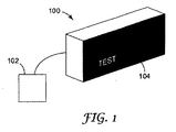
LEDを使用するアドレス指定可能な照明ユニット100の一例を、概略的に図1に示している。電源102は、表示パネル104に電力を供給する。表示パネル104は、個別にアドレス指定可能な発光素子のアレイを含む。表示パネル104上に所望のパターンを照明するように、電源102、またはパネル104内の制御回路は、個別の発光素子に選択的に電流を供給する。
An example of an
表示パネル104の一部を図2に示している。観察者が表示パネル104に近づくと、発光素子106の個別性がより明らかとなる。観察者がパネル104に十分近づくと、観察者は表示パネルの個別の発光素子をより容易に認識できるようになり、パネル上に表示されるメッセージの認識はより困難になる。たとえば、個別の要素106が「T」字型を形成しているが、この「T」は、さらに離れて「T」を観察するときほどには容易に識別できない。
A part of the
この問題の理由の一部は、ディスプレイ上の個別の発光素子106は、顕著な黒色の境界によって互いに分離されており、そのため近距離においては、観察者はこれらの発光素子を、パターンの一部としてよりも、分離した要素として見やすくなることにある。比較として、パネル200内の文字「T」の表示は、隣接する発光素子206を分離する暗い空隙が減少する場合に、情報が読みやすくなることを示している。
Part of the reason for this problem is that the individual light-emitting
別の実施形態においては、照明ユニット100は、できるだけ多量の光を提供できるように、すべての発光素子を単純に照明することができる。このような照明ユニットは、情報表示ではなく照明目的で使用することができる。
In another embodiment, the
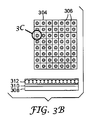
図3A〜3Bを参照しながら、照明ユニット300の構造の一実施形態をさらに説明する。照明ユニット300の表示パネル302は、多数のタイル304を含み、各タイル304は多数の発光素子306を含む。タイル306の層は、基体308と、ガイド層310と、場合によりコントラスト/投影フィルター312とを含む。
An embodiment of the structure of the
コントラスト/投影フィルター312は、i)反射周辺光の量を減少させるため、および/またはii)映写スクリーンとして機能できるように視野角を得るために使用される。周辺光の減少および視野角の選択は、照明ユニットの個別の用途、排除する必要がある多量の周辺光が存在するかどうか、または広い角度にわたって照明ユニットからの光を拡散させることが望ましいかどうかに依存する。たとえば、照明ユニットが屋外での情報表示用途に使用される場合、直射日光下でのコントラストを改善するために周辺光を減少させ、同時に、観察者が情報を見ることができる領域を増加させるために広い視野角も提供することが望ましいことがある。別の例において、照明ユニットが屋内で使用される場合、周辺光の排除は不要となることがある。
The contrast /
コントラスト/投影フィルター312が、周辺光の反射を減少させる場合、コントラスト/投影フィルターは、周辺光の反射量を減少させるために、反射防止特性を有することができ、たとえば反射防止層を含むことができる。フィルター312は、これに加えて、またはこれとは別に、周辺光の鏡面反射を軽減する防眩性を有することができ、たとえばつや消し面を有することができる。反射周辺光量を減少させる別の方法は、周辺光を吸収することである。フィルター312が視野角を提供する場合、このフィルターは、映写スクリーン、たとえばレンチキュラー映写スクリーン、またはビーズスクリーンとして機能する1つ以上の層を含むことができる。一部のレンチキュラースクリーンおよびビーズスクリーンでは、周辺光の減少と視野角との両方が提供される。図3Bおよび3Cに示されるこのようなスクリーンの一例は、ミネソタ州セントポールの3Mカンパニー(3M Company,St.Paul,Minnesota)より入手可能なビキュイティ(Vikuiti)(登録商標)XRVS型スクリーンである。このXRVSスクリーンでは、吸収材料層中に埋め込まれた透明な球体を介して光が屈折することによって視野角が得られ、この透明な球体は、スクリーンを通過する光に低損失経路を提供し、吸収材料は入射周辺光を吸収する。別の種類のフィルターは、コントラスト/投影フィルター中に、たとえば、所望の偏光状態で光を伝達する反射偏光子または吸収型偏光子などの偏光層を含むことができる。組み込むことができる他の種類のフィルターとしては、ビキュイティ(Vikuiti)(登録商標)サーキュラー・ポーラライザー(Circular Polarizer)(CP)層、またはビキュイティ(Vikuiti)(登録商標)ライト・コントロール・フィルム(Light Control Film)層が挙げられ、これらは、軸外観察からのプライバシーを提供する、および/またはディスプレイから反射される周辺光の量を減少させる。両方のビキュイティ(Vikuiti)(登録商標)層が3Mカンパニー(3M Company)より入手可能である。
If the contrast /
個別の発光素子306の高さにおいて、基体308上に1つ以上のLED320が配置される。発光素子306から単一色のみが発せられる必要がある場合、1つのみのLEDを使用することができるし、発光素子306によって発生される光学出力を増加させるために同じ種類の2つ以上のLEDを使用することもできる。発光素子から発せられる光の色を選択可能である場合は、異なるLEDを使用して異なる色を発生させることができる。異なるLEDを個別に制御することによって、発せられる光の色を制御することが可能となる。さらに、発光素子306が白色光を発することが望ましい場合、異なる色の光を発する多数のLEDを発光素子306に提供することができ、それらの複合作用によって、発せられた光を観察者が白色と認識する。白色光を発生させる別の方法は、比較的短波長の光を発する1つ以上のLED320を使用し、発せられた光を、燐光体波長変換器の使用により白色光に変換することである。白色光とは、人間の肉眼の赤、緑、および青の感覚器官を刺激して、通常の観察鎖が「白色」であると見なす外観が得られる光である。このような白色光は、赤色側(一般に温白色光と呼ばれる)または青色側に偏っている場合もある(一般に冷白色光と呼ばれる)。この光は、最大100の演色評価数を有することができる。
One or
LEDという用語は、たとえば、1種類以上のIII族元素と1種類以上のV族元素との組み合わせ(III−V半導体)から形成される種々の形態の無機半導体発光ダイオードを意味するために使用される。LEDにおいて使用できるIII−V半導体材料の例としては、窒化ガリウムまたは窒化インジウムガリウムなどの窒化物、ならびにリン化インジウムガリウムなどのリン化物が挙げられる。他の種類のIII−V材料を使用することもできるし、周期表の他の族の無機材料を使用することもできる。 The term LED is used to mean various forms of inorganic semiconductor light emitting diodes formed from, for example, a combination of one or more Group III elements and one or more Group V elements (III-V semiconductor). The Examples of III-V semiconductor materials that can be used in LEDs include nitrides such as gallium nitride or indium gallium nitride, and phosphides such as indium gallium phosphide. Other types of III-V materials can be used, and inorganic materials from other groups of the periodic table can also be used.
LEDは、パッケージ型LEDであってもよいし、または非パッケージ型LED、たとえば、LEDダイ、表面実装LED、チップオンボードLED、およびその他の構成のLEDであってもよい。LEDという用語は、燐光体とともに実装されたLEDまたは燐光体と関連するLEDも含み、この燐光体は、LEDから発せられた光を異なる波長の光に変換するために使用される。チップオンボード(COB)は、従来ワイヤボンディングなどを使用して基体に相互接続されたフェイスアップ接合(face−up−bonded)チップデバイスを使用する複合技術である。接続は、ワイヤボンディング、テープ自動ボンディング(tape automated bonding)(TAB)、またはフリップチップボンディングによって行うことができる。本明細書において示される大部分の例ではLEDダイが示されているが、これは限定を意図するものではなく、この段落に記載した他の種類のパッケージ型LEDを使用することもできる。 The LEDs may be packaged LEDs or non-packaged LEDs such as LED dies, surface mount LEDs, chip on board LEDs, and other configurations of LEDs. The term LED also includes an LED mounted with or associated with a phosphor, which is used to convert light emitted from the LED into light of a different wavelength. Chip-on-board (COB) is a complex technology that uses face-up-bonded chip devices that are interconnected to a substrate using conventional wire bonding or the like. The connection can be made by wire bonding, tape automated bonding (TAB), or flip chip bonding. Although most examples shown herein show an LED die, this is not intended to be limiting, and other types of packaged LEDs as described in this paragraph can also be used.
LED320から発せられた光を観察者の方向に向けるために、基体308上に反射層322を提供することができる。また、フィルムからの光を抽出し、場合によるスクリーン層312を通して観察者に光を向けるためにガイド層310は多数の光抽出機構324を含むことができる。光抽出機構324は、LED320またはその付近に集中する放射パターンをガイド層310上に配列させることができる。LED320から発せられた光がたどる光路は、観察者に向かう前に、ガイド層310内での反射を伴う場合がある。製造プロセスが、十分に大きな基体、レンズフィルム、およびスクリーン層を製造できるのであれば、タイル構造を省くことができる。
A
照明ユニット400の部分分解図を、図4Aに概略的に示している。照明ユニット400は、多数のLED420が上に配列された基体408を含む。基体408は、あらゆる好適な種類の材料から形成することができる。たとえば、基体408は、金属、セラミック、またはポリマーから形成することができる。ポリマー基体の特定の例の1つは、デラウェア州ウィルミントンのデュポン(Du Pont,Wilmington,Delaware)製造のカプトン(Kapton)ブランドのポリイミドなどのポリイミドである。基体408は可撓性の場合もあるし、剛性の場合もある。基体408は、たとえば、マサチューセッツ州ピッツフィールドのGEプラスチックス(GE Plastics,Pittsfield,MA)製造のポリカーボネートなどの透明材料から形成することもできる。
A partially exploded view of the lighting unit 400 is schematically illustrated in FIG. 4A. The lighting unit 400 includes a base 408 on which a number of
基体408とガイド層410との間に中間層422を導入することができる。ガイド層410は典型的には、LED420によって発せられる光に対して透明であり、たとえば、ポリカーボネート、ポリエステル、ウレタン、アクリレートなどの透明ポリマーから形成することができる。このポリマー材料の一覧は、好適なポリマー材料の網羅的な一覧を意図したものではない。
An
ガイド層410は、各LED420と関連する光抽出要素424のアレイを含むことができる。中間層422は、基体408上に配置されたLED420に対して位置合わせされるアパーチャー423を含み、これらはビアとも呼ばれる。中間層422は、波長LED420によって発せられる波長の光に対して反射性であってもよい。中間層422は、たとえば、ミネソタ州セントポールの3Mカンパニー(3M Company,St.Paul,Minnesota)より入手可能なビキュイティ(Vikuiti)(登録商標)ESRフィルムなどの多層ポリマー反射フィルムを含むことができる。中間層422は、拡散反射粒子、たとえば二酸化チタン粒子を含有するマトリックスなどの白色拡散反射体であってもよい。中間層422は、金属化層または多層誘電体コーティングなどの一部の他の種類の反射体を含むこともできることを理解されたい。中間層422は、たとえば感圧接着剤を使用して、基体408に接合することができる。アパーチャーは、たとえばレーザーフライス加工を使用して、中間層422中に形成することができる。
The
別の実施形態においては、中間層422が非反射であってもよい。このことは、強い周辺光を伴う用途に照明ユニットが使用される場合に特に有用である。非反射性中間層422は、ポリマーマトリックス中に分散した炭素粒子などの吸収性化学種を含むポリマー層から形成することができる。非反射性中間層は、照明ユニットによって反射する周辺光量を減少させることによって、LED420から発せられる光の視認性を増加させるのに役立つ。
In another embodiment, the
LED420の上にガイド層410を形成するためには、いくつかの異なる方法を使用することができる。一例は、LED420および/または中間層422の上に、あらかじめ提供された光抽出要素を有するシートとしてガイド層410を積層することである。別の例においては、LED420および/または中間層422の上にポリマー層をコーティングし、その場で光抽出要素を形成することによって、ガイド層410を形成することができる。これら2つの例の提示は、LED420の上にガイド層410を形成する方法の網羅的な一覧を提示することを意図したものではない。
Several different methods can be used to form the
LED420に入る電流およびLED420から出る電流を運ぶために、種々の層の上に導体を提供することができる。LED420に入る電流およびLED420から出る電流を運ぶために、たとえば、基体408、中間層422、および/またはガイド層410のいずれかの上に導体を提供することができる。導体は、たとえば銅から形成された金属トレースの形態をとることができる。図4Aに示される例においては、LED420に入る電流および/またはLED420から出る電流を運ぶために、基体408上に導体421が配置される。ワイヤボンド426を介して、基体408上の導体425にLED420がワイヤボンディングされる。LED420は、その下面上に形成される両方の電極を有するフリップチップの種類であってもよい。はんだリフロー、またはノースカロライナ州ケアリーのロード・コーポレーション(Lord Corp.,Cary,North Carolina)より入手可能なメテック・タイプ6144(Metech type 6144)などの導電性エポキシを使用した接続などのあらゆる好適な技術を使用して、導電体に対して電気接続を行うことができる。
Conductors can be provided on the various layers to carry current into and out of
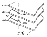
図4B〜4Eに関してこれより説明するように、LED420は、他の層の上に提供された導体と電気接続することができる。図4Bは、導体421が基体408上に提供され、別の導体431が中間層422の下面上に配置されている例を概略的に示している。図4Cは、導体421が基体408上に提供され、別の導体441が中間層422の上面上に配置されている例を概略的に示している。図4Dは、導体421が基体408上に提供され、別の導体451がガイド層410の下面上に配置されている例を概略的に示している。
As will now be described with respect to FIGS. 4B-4E, the
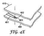
図4Eに概略的に示されている別の方法においては、層460に導体461および462の両方を提供することができ、これらは、層460の異なる面上に提供することもできるし、層460の同じ面上に適用することもできる。層460はアパーチャーまたは凹部423を含む。層460は、たとえば基体が反射材料で形成される場合に基体層であってもよいし、基体層(図示せず)を層460の下に提供できる場合には中間層であってもよい。アパーチャー423をブラインドホールにするために、導体461がアパーチャー423の開口部を覆うことができ、それによってアパーチャー423内の所定の位置にLEDが保持される。
In another method, schematically illustrated in FIG. 4E,
LED420によって発生した熱を除去するために、基体408の下面(図示せず)上に金属層を提供することができる。さらに、LED420によって発生した熱の拡散を促進するために、導体421に広面積パッド421aを提供することができる。一般に、LED420と観察空間との間の光路中に導体420がない場合、LED420からの熱の拡散を促進するために導体420の寸法がより大きくなってもよい。しかし、たとえばガイド層410の下面上または反射中間層422の上面上など、導体が光路内に配置される場合は、観察空間を通過する光に対する悪影響を軽減するために、導体の大きさを縮小することが一般に望ましい。
A metal layer can be provided on the lower surface (not shown) of the
図示されるように、LED420は、長方形パターン、または正方形パターンで基体408上に配列することができる。これによって、情報表示用途において縦および横の線の表示が容易になる。しかし、長方形または正方形のパターンが必要なのではなく、LED420は、たとえば六角形パターンなどの他のパターンで基体408上に配置することができる。発光素子の実際の形状は、正方形、長方形、円形、またはその他の形状であってよい。発光素子間の間隙、言い換えると、光がほとんどまたは全く発せられない発光素子間の領域は、輝度強化フィルムまたは投影フィルターを固定するためなどの接合面として使用することができる。
As shown, the
図4A〜4Dにおいては、ただ1つのLED420が各発光素子と関連しているが、各発光素子と関連する2つ以上のLED420が存在してもよい。たとえば、図4Fに概略的に示されるように、LED420は、互いに密接して取り付けられ異なる色を発するLEDダイ470などの複数のLEDを含むことができる。このような配列によって、白色光などの混合色の光を生成できるだけででなく、各LEDから発せられる光の相対量を変化させることによって、発せられる光の色合いを使用者が制御することができる。
In FIGS. 4A-4D, only one
以下に示す例においては、基体に直接取り付けられたチップ(ダイ)の形態でLEDが示されている。これは本発明の限定を意図するものではなく、他の形態のLEDも使用することができる。 In the example shown below, the LED is shown in the form of a chip (die) attached directly to the substrate. This is not intended to limit the invention, and other forms of LEDs can be used.
発光素子500の特定の一実施形態の断面を、図5Aにおいて概略的に示している。この実施形態においては、LED520は基体508に接合されている。中間層522はLED520と略同じ高さを有し、ガイド層510はLED520および中間層522の両方に接合することができる。LED520と基体508との間にワイヤボンドが存在する場合、そのワイヤボンド529は、中間層522を通過する別個のビア528内を通ってLED520と基体との間を通過することができる。ワイヤボンド529は、LED520と同じビア523の中を通ることもできる。
A cross section of one particular embodiment of light emitting device 500 is schematically illustrated in FIG. 5A. In this embodiment, the
LEDからの光が広範囲の角度にわたって発せられる場合、基体508から離れる方向で略上方に光が向かうようにLED520が配置される。LED軸520aは、基体508に対して垂直に位置するように示されているが、多くのLEDは、LED軸520aに対して対称に光を発する。LED軸520aに対して対称には光を発さない場合、LED520から光が発せられる方向の平均にLED軸が対応する。軸520aは、LED520によって発せられる最大強度の光の方向を表す必要はない。
When the light from the LED is emitted over a wide range of angles, the
別の実施形態の断面を、図5Bに概略的に示している。この実施形態においては、LED520が中間層522よりも高く、中間層522の上にガイド層510を維持するためにスタンドオフ530を使用することができる。スタンドオフ530は、LED520が接触する高さにガイド層510を維持することができるし、LED520と接触するよりも高い高さにガイド層510を維持することもできる。
A cross section of another embodiment is shown schematically in FIG. 5B. In this embodiment, the
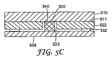
別の実施形態の断面を、図5Cに概略的に示している。この実施形態においては、中間層522の高さが、LED520の高さよりも低い。中間層522と基体508との間にスタンドオフ532が提供されている。中間層522をガイド層510の下面511と接合することができる。
A cross-section of another embodiment is schematically illustrated in FIG. 5C. In this embodiment, the height of the
LEDは、断面が正方形や長方形である必要はない。たとえば、図5Dに概略的に示されるように、LED520が異なる形状を有することができる。さらに、照明ユニットを組み立てるときのLED520と中間層522との間の位置合わせにおける制約を軽減するために、中間層522中のアパーチャーが、LED520よりも大きい寸法であってよい。
The LED need not have a square or rectangular cross section. For example, as schematically shown in FIG. 5D, the
別の実施形態の断面を、図5Eに概略的に示しており、この図ではLED520の一部が、ガイド層510中の凹部550内にある。この実施形態においては、LED520の側面から発せられる一部の光552は、ガイド層510内に向かい、ガイド層510に沿って案内される。LED520の上部から発せられる光554も、ガイド層510に沿って案内される場合がある。
A cross-section of another embodiment is schematically illustrated in FIG. 5E, where a portion of the
LED520とガイド層510との間の光結合は、LED520とガイド層510との間に配置された光結合材料540を使用することによって促進することができる。光結合材料540は、構造的完全性を増加させる接着特性を提供することもできる。
Optical coupling between the
光結合材料540は、組立工程中に種々の方法で適用することができる。ある方法では、ガイド層510を適用する前にLED520の上部に結合材料540を配置する。次にLED520の組立体の上にガイド層510を適用する。このような適用によって、典型的には、LED520を収容するビア523の中、および中間層522とガイド層510との間に広がるように、結合材料520が移動する。別の方法においては、LED520の上にガイド層510を適用し、次に、ガイド層510と中間層522およびLED520との間に、毛管作用によって結合材料540を移動させる。この方法においては、結合材料が、LED520を収容するビア523を充填、または部分的に充填することもできる。光結合材料540の一例は、ニュージャージー州クランベリーのノーランド・プロダクツ(Norland Products,Cranbury,New Jersey)より供給されるノーランド・タイプNOA81(Norland type NOA 81)光学接着剤である。
The
これより、LEDからの光を分散させる別の方法について、図6〜18を参照しながら説明する。これらの方法の多くでは、LEDからの光の一部は、ガイド層510内の下面または上面のいずれか、あるいはそれらの両方で反射し、そのためガイド層510は、LEDからの光を案内すると言うことができる。観察者に光が向かう前に、LEDから離れる光を側方に案内することは、光の拡散とも呼ばれ、このことは、照明ユニットの隣接する発光素子の間の暗い空隙の量を減少させるのに役立つ。LED520によって発せられた光のすべてがガイド層510内に案内される必要はないことを理解されたい。
Hereafter, another method for dispersing the light from the LED will be described with reference to FIGS. In many of these methods, some of the light from the LED is reflected on either the lower surface or the upper surface in the
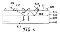
図6において、LED620は、基体608上に配置され、反射フィルムであってもよい中間層622によって囲まれている。LED620の上にはガイド層610がある。LED620からの光は、ガイド層610内に入る。LEDから離れているガイド層610の面には、光抽出機構624が提供されている。この特定の実施形態においては、光抽出機構624は、LED620の周囲に配置されるプリズム構造626を含む。プリズム構造626は、その中心にLED620を有するフレネルレンズとして形成することができる。LED620からの光630はガイド層610内に入る。一部の光632は、プリズム構造626を介して直接発せられる場合がある。他の部分の光634は、たとえばガイド層610の上面611で反射することによって、ガイド層610内に反射する場合がある。光634は、ガイド層610の下面612または中間層622で反射する場合もある。プリズム構造626によって、観察者に近づく方向で光634が向かう。
In FIG. 6, an
この実施形態および以下の実施形態においては、光は、中間層622によって反射してガイド層610内に戻る場合もあるし、あるいは内部反射および/またはガイド層610の下面612で反射することもできる。光が下面612で内部反射する場合、下面612上にも光抽出機構を提供することができる。光が中間層622によって反射する場合、中間層622上および/または下面612上にも光抽出機構を提供することができる。
In this and the following embodiments, light may be reflected by the
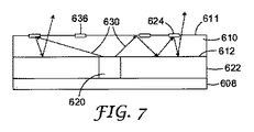
図7に概略的に示す実施形態においては、光抽出機構624は、ガイド層610の上面611上に提供された回折構造または拡散反射材料636を含む領域を含むことができる。光630はガイド層610内に案内される。しかし、回折構造または拡散反射材料636において回折または拡散反射が起こった後、光630は中間層622に向かい、中間層622によって光が反射して戻りガイド層610を通過して観察者に向かう。光が中間層622に向かい、さらに上面612を通過して観察者に向かうように、ガイド層610の表面611上の回折構造または拡散反射材料636の密度を選択することができる。
In the embodiment schematically illustrated in FIG. 7, the
図8に概略的に示す実施形態においては、光抽出機構624は、ガイド層610の上面611に貫入する抽出溝646を含む。抽出溝646は、上面611からの光を中間層622に向かわせ、中間層622で光が反射して戻り、ガイド層610を通過して観察者に向かわせるのに役立つ。
In the embodiment schematically illustrated in FIG. 8, the
図9に概略的に示す実施形態においては、光抽出機構は、ガイド層の上面611に貫入するくぼみ648を含む。くぼみ648は、中間層622から反射した光がガイド層の上面611を透過できるような角度で、上面からの光を中間層622に向かわせることができる。くぼみ648は、その表面に入射した光を、ガイド層610から直接出させることもできる。図8に示されるくぼみ648および溝646は、ガイド層から光を抽出して所望の照明プロファイルを得るためのあらゆるパターンでガイド層610上に組み込むことができる。
In the embodiment schematically illustrated in FIG. 9, the light extraction mechanism includes a
図10Aに概略的に示す実施形態においては、光抽出機構624は、光結合材料650の層と、光結合材料650に頂点が貫入している複数のプリズム型構造652とを含む。プリズム型構造652はベース層654に取り付けることができる。たとえば、プリズム型構造652は、ベース層654とともに成形することができるし、ベース層654に接合することもできる。光結合材料650は、たとえば、1〜20μmの範囲の厚さの薄い接着剤層であってよい。この特定の実施形態においては、光630は、ガイド層610を出て、結合材料650の上面651で全反射することができる。光630は中間層622に向かい、中間層622で光は上方に反射して戻る。ガイド層612の上面612に入射する光の一部は、プリズム型構造652と結合し、このプリズム型構造652によって、通常の観察者の方向の上方に光が反射する。ベース層654から発せられる光656を拡散させるために、ベース層654に、表面拡散体または体積拡散体を提供することができる。プリズム型構造652は、LED620を中心とするパターンに成形することができるし、他のパターンで提供することもできる。たとえば、プリズム型構造は線状であってもよい。
In the embodiment schematically illustrated in FIG. 10A,
図10Aに示す実施形態の一変形においては、たとえば図10Bに示されるように、ベース層の出力側の近くにコントラスト/投影フィルター658を提供することができる。
In a variation of the embodiment shown in FIG. 10A, a contrast /
光の配向または再配向のために、ガイド層の上に1つ以上の調光フィルムを使用することができる。たとえば、基体608に対して垂直方向により近い方向に光を向けるために、ミネソタ州セントポールの3Mカンパニー(3M Company,St.Paul,Minnesota)より商品名BEF(登録商標)で入手可能な1つ以上の輝度強化フィルムを使用することができる。輝度強化フィルムは、典型的には、複数のプリズム屈折要素を含み、プリズム要素の底面から照明すると、透過光は軸に対してより平行に近い方向に屈折する。図11に示される例においては、回折性光抽出要素636を使用する発光素子は、軸660に対して第1の方向で、ガイド層610から光を発する。第1の輝度強化層662を出るときに、光667は、第1の方向よりも軸666に近い第2の方向に屈折する。ある実施形態においては、1層のみの輝度強化フィルム662が使用される。典型的には、第1の輝度強化フィルムのプリズムにはリブが取り付けられ、それによって1層の輝度強化フィルムは、光を一方向にのみ再配向する。場合により、輝度強化フィルムの第2の追加層664を使用することができ、この場合、輝度強化フィルムの第2の層664のリブ付きプリズムは、第1の層662のリブ付きプリズムに対して垂直に向けられ、輝度強化フィルムの2つの層662および664を組み合わせることで、2つの寸法で軸666に向かうように光を再配向させる。
One or more light management films can be used on the guide layer for light orientation or reorientation. For example, one that is available under the trade name BEF® from 3M Company, St. Paul, Minnesota, St. Paul, Minnesota, to direct light in a direction closer to the vertical direction with respect to
たとえば図12に概略的に示すように、調光フィルム662および664からの出力側にコントラスト/投影フィルター668を提供することができる。一部の用途においては、ミネソタ州セントポールの3Mカンパニー(3M Company,St.Paul,Minnesota)より供給されるビキュイティ(Vikuiti)(登録商標)DBEFフィルムなどの多層光学フィルム(MOF)反射偏光子などの反射偏光層を、発光素子の上に提供することができる。反射偏光子は、ある偏光状態の光を透過し、それと直交する偏光状態の光を反射し、LCDディスプレイの背面照明など、偏光を提供するために発光素子が使用される場合に、このような偏光子を使用することができる。反射偏光子によって反射される偏光状態の光は、反射して基体608に戻る。反射偏光子によって反射された光を、ある程度偏光解消して反射させるために、層の1つ、たとえば中間層622を処理することができ、それによって、反射偏光子によって反射された光を再利用して、最終的に反射偏光子を通過させることができる。
For example, as shown schematically in FIG. 12, a contrast /
ガイド層610は、平行な表面を有する必要はない。言い換えると、表面611および612は互いに対して非平行であってもよい。このような一実施形態を、図13に概略的に示しており、この場合、光抽出機構は、下面612に対しても基体608に対しても非平行である上面611である。光630は、上面611において内部反射して、下面612に向かい、下面または中間層622によって光670として反射する。しかし、上面611は下面612と平行でないため、反射光670は、LEDからの光630として入射する角度と同じ角度では上面611には入射しない。臨界角未満の入射角で反射光670が上面611に入射する場合、反射光670は光672として上面611を透過する。BEF(登録商標)などの別の層(図示せず)を使用することで、基体608に対してより垂直となる方向に光672を向けることができる。
The
LED620からの光をフィルム610に沿う方向に向かわせ、それによってガイド層610によって案内される光の量を増加させるために、ガイド層610に成分674を提供することができる。図示される実施形態においては、成分674は、LED620の上方に位置する凹部を含む。LED620からの光676は、凹部表面で内部反射して、フィルム610に沿った方向に向かう。凹部表面に対する入射角が十分大きい場合、その光は全反射する。光676は、傾斜した上面611から反射した後で、フィルム610から離れる方向に向かうことができる。基体608に対して平行の複数の表面をガイド層610が有する、本明細書において説明される発光素子の別の実施形態においても、成分674を使用することができる。
A
ガイド層の表面が平行ではない別の実施形態を、図14Aに概略的に示している。この実施形態においては、上面611は基体608に対して平行であるが、下面612は基体608に対して平行ではない。この場合、光抽出機構は下面612を含む。光630はガイド層610の上面611によって内部反射して、下面612に向かう。この光は、下面612から上面611の方に戻る。下面612からの光が、臨界角未満の入射角で上面611に入射する場合に、光680は上面611を透過する。
Another embodiment in which the surface of the guide layer is not parallel is shown schematically in FIG. 14A. In this embodiment, the
様々な種類の反射体を下面612上に使用することができる。たとえば、下面612に反射膜をコーティングすることができる。他の方法としては、下面612上に構造を提供することが挙げられる。たとえば、図14Bに概略的に示すように、1つ以上のステップ682を下面612に提供することができる。ステップ682は、一部の入射光686を全内部反射させるのに望ましい角度に設定される。別の方法においては、屈折および全反射の組み合わせによって入射光686を再配向させる一連の要素684、たとえばプリズム要素を下面612に提供することができる。ガイド層610の下面612を透過した光は、中間層622によって反射し、ガイド層610を透過して戻ることができる。
Various types of reflectors can be used on the
抽出機構は、ガイド層610の上面上に配置する必要はなく、ガイド層610下面上および/または中間層622上に提供することができる。このような配置の一例を図15Aに概略的に示しており、この図では、反射中間層622に非平面上表面構造690が提供されている。一部の光692は、ガイド層610によって案内されて、表面構造690上に入射する。表面構造690から反射した光の一部は、ガイド層610の上面611に向かい、さらに観察者に向かう。多数の様々な技術を使用して、表面構造694を中間層622に導入することができる。中間層622中に使用できるようなポリマー反射体上に構造を形成するいくつかの方法が、米国特許第6,045,894号明細書および第6,096,247号明細書に記載されている。
The extraction mechanism need not be located on the upper surface of the
別の例を図15Bに概略的に示しており、この図では、反射性中間層622の上面、および/またはガイド層610の下面に、白色に着色した材料などの拡散反射性光抽出材料のパッチ695が提供されている。パッチ695上に入射する少なくとも一部の光は、鏡面反射せずに拡散反射し、一部の光697はガイド層610の外に向かうことができる。他の種類の光抽出機構を、中間層622の上面上、またはガイド層610の下面上に提供することができ、ガイド層610の上面上の光抽出機構とともに提供することもできる。
Another example is schematically illustrated in FIG. 15B, where diffuse reflective light extraction material, such as a white colored material, is applied to the upper surface of the reflective
1種類のみの抽出機構を有する例で、本明細書に記載される光抽出機構を説明してきた。本明細書に記載される種々の光抽出機構は、単独で使用することもできるし、異なる種類の光抽出機構と組み合わせることもできることを理解されたい。 The light extraction mechanism described herein has been described with an example having only one type of extraction mechanism. It should be understood that the various light extraction mechanisms described herein can be used alone or in combination with different types of light extraction mechanisms.
LED620によって発生した光の大部分は、ガイド層610を直接通過できる方向に伝播し、これは、発光素子の中央の明るい箇所として観察者が認識することができる。ガイド層の使用に加えて、横方向に光を拡散させるために他の方法を使用することができる。このような方法の1つは、図13に示される成分674に関して既に説明しており、この場合、光は、凹部表面で内部反射し、それによってガイド層610の面に略沿った方向に向かう。横方向に拡散した後、光はガイド層から抽出される。
Most of the light generated by the
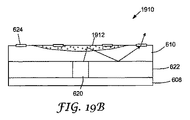
LED620からの光をガイド層610内に拡散させる別の方法を、これより図19Aを参照しながら説明する。LED620から遠い側のガイド層610の上に、体積拡散体などの拡散体1902が配置される。拡散体1902が体積拡散体である場合、その体積拡散体をガイド層610内に配置することができる。拡散体1902は、LEDからガイド層610を直接通過する光の量を減少させ、それによって発光素子からの出力を均一化するために使用される。拡散体1902は一部の光1904を側方に拡散させ、抽出機構624を介して、別の位置でガイド層から抽出することができる。
Another method of diffusing light from the
拡散体1902の拡散力は、発光素子から発せられる光の所望のプロファイルを向上させるように、空間的に調整することができる。たとえば、LED620の上に発生される光の量を減少させ、発光素子の周囲に光を拡散させることが望ましい場合、拡散体1902の拡散力はLED620の上で最大にする。図示される実施形態においては、拡散体1902はLED620の上で最も厚く、拡散体厚さ1902は、発光素子1900の端部に向かうにつれて薄くなる。拡散体1902の拡散力は、体積拡散体中の拡散粒子の密度を空間的に変化させることによって調整することもできる。図示される実施形態においては、拡散体1902の厚さが、発光素子1900の中心から直線的に変化している。
The diffusing power of the
図19Bに概略的に示す別の実施形態においては、拡散体1912の厚さは、発光素子1910全体にわたって、位置に関して非線形的に変動している。さらに、拡散体1912は、発光素子1910全体の領域に延在することもできるし、しないこともできる。図示される実施形態においては、拡散体1912は発光素子1910全体には延在していない。
In another embodiment schematically illustrated in FIG. 19B, the thickness of the
LED付近で光束が大きくなる傾向にあり、その結果、LED付近で発せられる光の量は、LEDから離れた場所よりもはるかに多くなりうる。このように発せられる強度プロファイルの一例を、図16Aの曲線(a)で概略的に示している。 There is a tendency for the luminous flux to increase near the LED, so that the amount of light emitted near the LED can be much greater than the location away from the LED. An example of the intensity profile thus generated is schematically shown by a curve (a) in FIG. 16A.
発光素子から発せられる光の強度プロファイルをより均一にするために、LED自体に近い位置での光の抽出を減少させ、LEDから離れた光抽出要素の位置での光抽出量を増加させるために、光抽出機構を配置または適合させることができる。このことを、図16Aを参照しながらさらに説明するが、この図は、発光素子1600を概略的に示しており、発光素子1600の中央におけるLED1620の位置と、LED1620の周囲で半径方向に配列された光抽出機構1624とが示されている。図示される実施形態においては、光抽出機構の密度は、LED1620から半径方向に離れるにしたがって増加している。光抽出密度を適切に選択することで、たとえば曲線(b)(破線)に示されるように、発光領域上でより均一な発光強度プロファイルを得ることができる。さらに、発光素子1600上の光抽出の不均一性が減少するように、抽出機構の抽出強度を、LED1620からの距離が増加するにつれて変動させることができる。たとえば、抽出機構の大きさを変動させることによって、抽出強度を調整することができる。
In order to make the intensity profile of the light emitted from the light emitting element more uniform, to reduce the light extraction at a position close to the LED itself and to increase the light extraction amount at the position of the light extraction element away from the LED The light extraction mechanism can be arranged or adapted. This will be further explained with reference to FIG. 16A, which schematically shows the
発光素子から発せられる光の強度プロファイルを制御するように、上面および下面の抽出機構、たとえば、上面上に形成されるプリズム構造、拡散構造、抽出溝、上面中に貫入するプリズム構造、およびガイドフィルム上の非平行表面などのあらゆる種類の抽出機構を配置することができる。さらに、ガイドフィルム上の表面構造を伴う非平行表面など、異なる種類の抽出機構の組み合わせを使用することができる。抽出機構は、比較的均一なプロファイルの照明プロファイル、または他の望ましいプロファイルが得られるように配列することができる。用語「均一」とは、LEDの上の領域がその周辺領域よりもあまり明るくならない比較的平坦な照明プロファイルを意味する。 Top and bottom extraction mechanisms, such as prism structures formed on the top surface, diffusion structures, extraction grooves, prism structures penetrating into the top surface, and guide films so as to control the intensity profile of light emitted from the light emitting elements Any kind of extraction mechanism can be placed, such as the non-parallel surface above. In addition, combinations of different types of extraction mechanisms can be used, such as non-parallel surfaces with surface structures on the guide film. The extraction mechanisms can be arranged to obtain a relatively uniform profile illumination profile, or other desired profile. The term “uniform” means a relatively flat illumination profile where the area above the LED is not much brighter than its surrounding area.
光抽出機構は、LED周囲で放射対称に配列される必要はなく、他の形状で配列することもできる。そのような形状の一例を図16Bに概略的に示しており、この図は、LED1620の周囲に略正方形のパターンで配列された光抽出機構1624を示している。
The light extraction mechanisms need not be arranged radially symmetrical around the LED, but can be arranged in other shapes. An example of such a shape is schematically illustrated in FIG. 16B, which shows
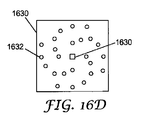
光抽出機構は、LEDの周囲に連続的に配列される必要はなく、不連続であってもよい。不連続な光抽出機構1634の一例を図16Cに概略的に示しており、この図では、回折領域または拡散反射パッチなどの不連続光抽出機構1624が、図16Bに示されるパターンと部分的に対応するパターンで配列されている。不連続な光抽出機構1642のパターンの別の例を図16Dに概略的に示している。所望の光抽出プロファイルに従って、多くの異なる種類のパターンを使用できることが理解できるであろう。
The light extraction mechanism need not be continuously arranged around the LED, but may be discontinuous. An example of a discontinuous light extraction mechanism 1634 is schematically illustrated in FIG. 16C, where a discontinuous
光抽出要素の印刷パターンを使用する一実施形態の発光素子2000を、図20Aに概略的に示している。シート2002は、少なくとも1つの表面上に拡散反射領域2004が配列されている。シート2002をガイド層610に十分接近させると、ガイド層610内の光2006がシート2002と結合して、拡散反射領域2004と相互作用する。したがって、拡散反射領域2004を光抽出機構として使用することができる。別の実施形態においては、ガイド層610の上面611の上に拡散反射領域を直接提供することができる。
One embodiment of a
拡散反射領域2004は、たとえば、シート2002上にドットの配列として印刷された白色顔料を含むことができる。LED620から直接透過する光2008の量を減少させ、LED620から離れた距離でガイド層から抽出するために光2006の横方向への拡散を増加させるように、拡散反射領域2004にパターンを形成することができる。このパターン形成は、たとえば、拡散反射材料の厚さを変動させることによって、表面611上に提供される拡散反射領域の表面密度を変動させることによって、拡散反射する材料の密度を変動させることによって、またはこれらの異なる方法の組み合わせによって行うことができる。図示される例においては、LED620の上の拡散反射領域2004aの程度(表面密度)は、発光素子2000の端部に近い拡散反射領域2004bの程度よりも大きく、そのため、LED620による直接照明がより明るい領域でのガイド層上側における拡散反射量が、LEDの直接照明があまり明るくないガイド層上側の他の領域における拡散反射量よりも多くなる。拡散反射領域は、拡散反射ではなく一部の光が通過するという点において、ある程度半透明であってよい。LED620からの光2008が、拡散反射領域2004aを通過するように示している。
The diffuse
種々の調光フィルム層2010は、ガイド層610から離れた後の光に影響を与えるために使用することができる。たとえば、層2010は、輝度強化フィルム層、交差した輝度強化フィルム層、反射偏光フィルム、またはそれらの組み合わせを含むことができる。層2010は他のフィルターおよびスクリーン層を含むこともできる。
Various light management film layers 2010 can be used to affect the light after leaving the
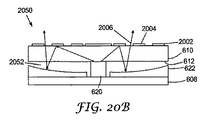
図20Bは、別の例の発光素子2050を示しており、ガイド層610の上面に拡散反射領域2004が直接適用されている。また、この発光素子は、ガイド層610の下面612と中間層622との間に間隙2052を含む。この場合、中間層622は反射性であり、そのため、下面612を通過して拡散反射した光2006は、逆向きに反射してガイド層を通過する。反射した光2006は、ガイド層を出て、さらに、拡散反射領域2004を通過したり、拡散反射領域2004の間を通ったりすることができる。
FIG. 20B shows another example of the
中間層622は、たとえば図20Aに示されるように平坦かつ平行であってもよいし、たとえば図20Bに示されるように湾曲していてもよい。湾曲した反射中間層は、成形品の上にESRフィルムを配置することによって形成することができる。間隙および湾曲した中間層は、上記または下記の異なる実施形態の発光素子中に存在できることを理解されたい。
The
明るいところでLED620の位置を観察者が見づらくなるように、シート2002を拡散体として使用することもできる。このような使用の一例を、図20Cに概略的に示している。間隙2012がシート2002をガイド層620から分離しており、光抽出機構624を使用することによって、光がガイド層から出ていく。この光抽出機構は、前述のいずれかの種類の光抽出機構であってよい。拡散反射領域2004に入射する少なくとも一部の光2014は拡散反射してガイド層610を通過し、中間層622に到達する。この光2014は中間層622によって反射し、ガイド層610およびシート2002を通過する。たとえば図20Dに概略的に示されるように、光2014をさらに拡散させるために、バルク拡散体などの拡散体2016を使用することもできる。
The
シート2002が、ガイド層610と光学的に接触しているか、ガイド層と分離しているかとは無関係に、拡散反射領域2004の位置および密度は、所望の出力照明プロファイルを実現するために調整することができる。
Regardless of whether the
1つの発光素子からの光は、隣接する発光素子を通過してもよい。しかし、情報表示などの一部の用途においては、隣接する発光素子間を光が通過するのを防止することが望ましい場合がある。このような隣接する発光素子間のクロストークを軽減する方法の1つは、光が発光素子の端部に到達する前に、LEDからのすべての光をガイドフィルムから離れるようにすることである。 Light from one light emitting element may pass through an adjacent light emitting element. However, in some applications such as information display, it may be desirable to prevent light from passing between adjacent light emitting elements. One way to reduce such crosstalk between adjacent light emitting elements is to allow all light from the LED to leave the guide film before the light reaches the edge of the light emitting element. .
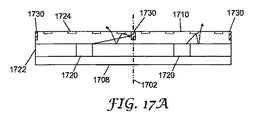
これより、図17A〜17Dを参照しながら、隣接する発光素子間のクロストークを軽減するための別の方法を説明する。これらの図面においては、隣接する発光素子が破線1702で分離されている。各発光素子は、中間層1722と中間層の上のガイド層1710とを有する基体1708上に配置された少なくとも1つのLED1720を含む。LED1720からの光はガイド層1710に入る。それぞれの場合で回折性光抽出要素1724が示されているが、他の種類の光抽出要素を使用することもできる。
Hereafter, another method for reducing crosstalk between adjacent light emitting elements will be described with reference to FIGS. In these drawings, adjacent light emitting elements are separated by a
図17Aに概略的に示す方法においては、隣接する発光素子の間に反射壁1730が配置されている。反射壁1730は、ガイド層1710中の溝の中に配置される反射材料を使用して形成することができる。この反射材料は、二酸化チタン(TiO2)、硫酸バリウム(BaSO4)、または酸化アルミニウム(Al2O3)などの高屈折率粒子を、ポリエステル(たとえばPENまたはPET)、ポリメタクリル酸メチル、ポリカーボネート、ポリウレタン、環状ポリオレフィンなどのポリマーマトリックス中に含むことができる。上記の溝は、ガイド層が製造されるときに、たとえば圧縮成形、注型および硬化、射出成形などによって、ガイド層中に形成することができる。
In the method schematically shown in FIG. 17A, a reflecting
図17Bに概略的に示す方法において、反射中間層1722には、上方に延在するリブ1740が提供されている。前段落に挙げた成形方法の1つなどによって、中間層1722の上にガイド層1710が形成される。リブ1740は、隣接する発光素子の間の反射壁として機能する。
In the method schematically illustrated in FIG. 17B, the reflective
これより図17Cに関して説明するように、LED1720が発光素子の中央に位置する必要はない。たとえば、左の発光素子1750中のLED1720は、発光素子1750の側面に配置されており、発光素子の端部またはコーナーに接近して配置することもできる。光抽出機構1724は、LED1720が中央から外れて配置されることで生じる光のパターンで受け取った光を配向させるように配置され配列される。
Thus, as will be described with respect to FIG. 17C, the
さらに、図面の右側の発光素子1752で示されるように、発光素子内にLED1720を2つ以上の位置で配置することができる。図示される実施形態においては、発光素子1752のいずれかの側面に1つずつで、2つのLEDが存在する。発光素子1752は、他の数のLED1720を含むこともできる。たとえば、発光素子1752が4つの側面を有する場合、LED1720は、発光素子1752の4つの端部に沿って配置したり、発光素子1752の4つのコーナーに配置したりすることができる。光抽出機構1724は、LED1720の特定の配置によって得られる光のパターンで受け取った光を配向させるように発光素子1752内に配置され配列される。
Further, as shown by the
図17Dに概略的に示す別の方法においては、2つの発光素子1762と1764との間の位置1760で、ガイド層1710の厚さが減少している。このようにガイド層の厚さを減少させることによって、ガイド層1710内で、1つの発光素子から隣接する発光素子に通過する光が、排除されないとしても、減少する。ガイド層の厚さの減少は、たとえば、隣接する発光素子の間に溝がある溝パターンのガイド層へのエンボス加工によって実現することができる。
In another method schematically illustrated in FIG. 17D, the thickness of the
別の実施形態の発光素子1800を図18Aに概略的に示しており、この図は並列する2つの発光素子を示している。この実施形態においては、LED1820は基体1808上に配置されている。光学シート1822は、LED1820に収容するためのアパーチャーを有し、このため、LED1820はアパーチャーを貫通している。したがって、基体1808は、シート1822の一方の側にあり、LED1820の発光部分は、アパーチャーを通過して光を発するための透明な経路を少なくとも有するか、あるいは、図示されるようにそれ自体がアパーチャーを貫通してもよい。
Another embodiment of a
シート1822には、ダイオード1820によって発せられる光を反射する反射面1824が提供されている。反射面1824は、所望の方向に光を向けるように湾曲している。たとえば、反射面は放物面、楕円であってよいし、他の形状を有することもできる。反射面1824は、成形フィルム上に形成された金属化面であってもよいし、多層反射体、たとえば真空めっきされた誘電性反射体または多層ポリマー反射体であってもよい。反射面1824は、シート1822上に堆積させることができる。別の方法においては、シート1822自体が、反射材料で形成されてもよく、たとえばミネソタ州セントポールの3Mカンパニー(3M Company,St.Paul,Minnesota)より入手可能なESR(登録商標)フィルムを打ち抜くことができる。
The
LED1820は、基体1808に取り付けられる下面上に両方の電気接点を有するフリップチップ型LEDであってよく、その場合、基体1808は、LED1820の正と負の両方の接点のための導体を有することができる。
The
LED1820および反射面1824の上の空間1826は、空気中であってもよいし、透明な材料を充填してもよい。たとえば、LED1820および反射面1824の上の所定の位置に透明材料を成形することができる。さらに、反射面1824によって反射した後の光を拡散させるために、シート1822の上に拡散体またはスクリーンフィルム1830を配置することができる。
A
別の実施形態の発光素子1850を図18Bに概略的に示している。この実施形態においては、反射面1824と拡散体またはスクリーン層1830との間にレンズを含んでいる。図示される実施形態においては、これらのレンズは、プリズムレンズ、たとえばフレネルレンズとして、レンズシート1852上に形成されている。しかし、他の種類のレンズを使用できることは理解できるであろう。たとえば、空間1826に透明材料が充填される場合、その透明材料の表面上にレンズを形成することができる。
Another embodiment of a
本明細書において説明される様々な種類の発光素子のそれぞれを、たとえば情報表示または空間照明に使用される照明ユニットに組み込むことができる。LEDダイは典型的にはわずか約300μmの厚さであり、ガイド層はLEDダイの表面上にあるため、これらの構造体を非常に小型化することができる。したがって、このような構造体の厚さは、わずか約1または2ミリメートルにすることができる。このため、照明ユニットを可撓性にしたり、非平面状形状にしたりする可能性が得られる。たとえば、照明ユニットは、円筒形などの形態に巻き付けることができる。照明ユニットは剛性であってもよい。 Each of the various types of light emitting elements described herein can be incorporated into a lighting unit that is used, for example, for information display or spatial lighting. Since the LED die is typically only about 300 μm thick and the guide layer is on the surface of the LED die, these structures can be very miniaturized. Thus, the thickness of such a structure can be only about 1 or 2 millimeters. For this reason, the possibility of making the lighting unit flexible or non-planar is obtained. For example, the lighting unit can be wound in a form such as a cylindrical shape. The lighting unit may be rigid.
一部の実施形態の照明ユニットについて、コントラスト/投影フィルターを含むとして前述しているが、希望するなら、あらゆる異なる種類の照明ユニットに、コントラスト/投影フィルターを提供できることを理解されたい。 Although the lighting unit of some embodiments has been described above as including a contrast / projection filter, it should be understood that a contrast / projection filter can be provided for any different type of lighting unit, if desired.
所定の照明用途においては、必要なLED数を決定する場合に、必要な輝度、照明装置の画素数、および照明装置の全面積のすべてが考慮される。2つの異なる照明用途の例を以下に説明する。 For a given lighting application, all of the required brightness, the number of pixels in the lighting device, and the total area of the lighting device are taken into account when determining the number of LEDs required. Examples of two different lighting applications are described below.
実施例1:天井照明
この実施例は、対角線が70インチ(178cm)であり、アスペクト比が5:1である照明器具について検討する。この実施例で、100Wの入力を使用して70L/W、すなわち7000ルーメンの2つの蛍光灯、光が得られる器具の設計を考慮している。
Example 1 Ceiling Lighting This example considers a luminaire with a diagonal of 70 inches (178 cm) and an aspect ratio of 5: 1. This example considers the design of an instrument capable of obtaining two fluorescent lamps, light of 70 L / W, ie 7000 lumens, using a 100 W input.
想定されるLED特性を表Iに示す。これらの特性は、カリフォルニア州サンノゼのルミレッズ・ライティングLLC(Lumileds Lighting LLC,San Jose,California)より入手可能な1mm平方のルクセオン(Luxeon)白色LEDの特性と類似のものである。 The expected LED characteristics are shown in Table I. These characteristics are similar to those of a 1 mm square Luxeon white LED available from Lumileds Lighting LLC (San Jose, Calif.) Of San Jose, California.
LEDは最大電力の2/3で動作すると仮定し、したがって実電流は最大電流未満となる。計算した照明ユニット設計を表IIにまとめている。 The LED is assumed to operate at 2/3 of the maximum power, so the actual current will be less than the maximum current. The calculated lighting unit design is summarized in Table II.

したがって、この実施例において、各発光素子が17.4cm2以下の面積を有し、全面積が0.6m2である発光素子のシートによって、蛍光灯および同じ面積の1組の蛍光灯および関連する照明光学系と同じ程度の光が得られる。スクリーンには、適切な調光フィルムおよび/または投影フィルターを通して60°の円錐で光が向けられると仮定している。発せられる光の立体角および記載の吸光によって、完全ランベルト放射体(perfect Lambertian emitter)に対して1.07の軸上利得(axial gain)が得られる。 Therefore, in this embodiment, each light emitting element has an area of 17.4 cm 2 or less, and the sheet of the light emitting element having a total area of 0.6 m 2 , the fluorescent lamp and a set of fluorescent lamps of the same area and related The same level of light as the illumination optical system is obtained. It is assumed that the screen is directed through a suitable dimming film and / or projection filter with a 60 ° cone. The solid angle of the emitted light and the light absorption described gives an axial gain of 1.07 for a perfect Lambertian emitter.
実施例2 液晶ディスプレイ用のRGBバックライト
この実施例においては、対角23インチの液晶ディスプレイ(LCD)用のバックライトとして照明ユニットを使用する。各発光素子は、1つの赤、2つの緑、および1つの青の4つのLEDダイを含む。異なるLEDダイを能動的に制御することによって、バックライトの色を制御することができる。この実施例の設計においては、バックライトは6500Kの色温度を有する。
Example 2 RGB backlight for liquid crystal display In this example, an illumination unit is used as a backlight for a 23 inch diagonal liquid crystal display (LCD). Each light emitting element includes four LED dies, one red, two green, and one blue. By actively controlling different LED dies, the color of the backlight can be controlled. In this example design, the backlight has a color temperature of 6500K.
この照明ユニットは、1枚のシートの輝度強化フィルムを使用して、56°(最大半減、半角)の水平視野角および37°(最大半減、半角)の垂直視野角が得られると仮定している。このバックライトから発せられる全光束は約1560ルーメンであり、軸上輝度は約5191カンデラ/m2である。この実施例のバックライトユニットの計算した特性を表IVに示す。 This lighting unit is assumed to use a single sheet brightness enhancement film to obtain a horizontal viewing angle of 56 ° (maximum half, half angle) and a vertical viewing angle of 37 ° (maximum half, half angle). Yes. The total luminous flux emitted from this backlight is about 1560 lumens, and the on-axis luminance is about 5191 candela / m 2 . The calculated characteristics of the backlight unit of this example are shown in Table IV.
したがって、本発明は、LCDディスプレイのバックライトとして効果的に使用することができる。このようなバックライトは、LCDディスプレイを、フィールドシーケンシャルカラーで動作させることができ、すなわち、LCDを異なる色の光で順次照明することができる。このようなLCDの照明方法では、カラーLCDディスプレイ中のカラーフィルターが不要となるので、全体の効率が増加し、コストが削減される。光学補償ベンド(optically compensated bend)(OCB)モードLCDは、応答時間が短いので、フィールドシーケンシャルカラー照明モードで動作すると特に有用である。 Therefore, the present invention can be effectively used as a backlight of an LCD display. Such a backlight can operate the LCD display in a field sequential color, i.e., sequentially illuminate the LCD with different colors of light. Such an LCD illumination method eliminates the need for a color filter in a color LCD display, thus increasing overall efficiency and reducing costs. Optically compensated bend (OCB) mode LCDs are particularly useful when operated in a field sequential color illumination mode due to their short response times.
さらに、上記のようなバックライトは、ディスプレイの異なる領域が異なる強度で照明されるように制御することができる。これは、たとえば、画像の一部が非常に明るく、その画像の別の部分が非常に低くなる高いコントラストを有する画像を表示する場合などに好都合となりうる。画像の暗い部分を照明するLEDの輝度を下げたり、さらには照明を停止したりすることもでき、それによって画像の暗い領域がさらに暗く見えるようになる。 Furthermore, the backlight as described above can be controlled so that different areas of the display are illuminated with different intensities. This can be advantageous, for example, when displaying an image with high contrast where one part of the image is very bright and another part of the image is very low. The brightness of the LED that illuminates the dark portion of the image can be reduced, or even the illumination can be turned off, thereby making the dark areas of the image appear darker.
本発明は、上記の特定の実施例に限定されるものと見なすべきではなく、むしろ、添付の特許請求の範囲において適切に提示される本発明のすべての態様を含むものと理解すべきである。種々の変更、等価の方法、および本発明を適用できる多数の構造は、本明細書を検討することによって、本発明に関する当業者には容易に明らかとなるであろう。特許請求の範囲は、このような変更および機構を含むことを意図している。 The present invention should not be construed as limited to the particular embodiments described above, but rather should be construed to include all aspects of the present invention as appropriately presented in the appended claims. . Various modifications, equivalent methods, and numerous structures to which the present invention can be applied will be readily apparent to those of skill in the art upon reviewing the present specification. The claims are intended to cover such modifications and mechanisms.
Claims (89)
前記LED上に配置された光学シートであって、前記LEDから前記光学シートの一方の面に入る光の少なくとも一部が、前記光学シート内で、前記基体に対して略平行方向に案内される光学シートとを含む、発光のための光学アセンブリ。 An array of inorganic light emitting diodes (LEDs) attached to a substrate, wherein the LEDs emit light in a direction substantially perpendicular to the substrate;
An optical sheet disposed on the LED, wherein at least a part of light entering the one surface of the optical sheet from the LED is guided in a direction substantially parallel to the base in the optical sheet. An optical assembly for light emission comprising an optical sheet.
無機発光ダイオード(LED)のアレイであって、異なるLEDが、前記発光システムのそれぞれの発光素子に対応しているアレイと;
前記LED上に配置されたライトスプレッダーシートとを含み、前記LEDから前記ライトスプレッダーシートに入った光が、前記発光システムの前記それぞれの発光素子に対応する領域上の前記スプレッダーシート内部で横方向に拡散し、前記ライトスプレッダーシートが、前記拡散した光出力を前記スプレッダーシートの外に配向させる光配向構造を含む、システム。 A light emitting system having a plurality of individually illuminated light emitting elements,
An array of inorganic light emitting diodes (LEDs), wherein different LEDs correspond to respective light emitting elements of the light emitting system;
A light spreader sheet disposed on the LED, the light entering the light spreader sheet from the LED laterally within the spreader sheet on an area corresponding to the respective light emitting elements of the light emitting system. A system that diffuses and the light spreader sheet includes a light orientation structure that directs the diffused light output out of the spreader sheet.
略1つの発光方向に光を発する無機発光ダイオード(LED)のアレイと;
前記LEDの前記アレイを横断する方向で側方に光を拡散させるための光拡散手段と;
前記光拡散手段からの光を所望の照明方向に配向させるための光配向手段とを含む、システム。 A light emitting system having a plurality of individually illuminated light emitting elements,
An array of inorganic light emitting diodes (LEDs) that emit light in approximately one emission direction;
Light diffusing means for diffusing light laterally in a direction transverse to the array of LEDs;
And a light orientation means for orienting light from the light diffusing means in a desired illumination direction.
略1つの発光方向に光を発するために基体上に配列された無機発光ダイオード(LED)のアレイと;
前記LEDとともに配置される反射体アレイであって、前記反射体は、反射シートの個別の部分を画定し、前記反射体はそれぞれのアパーチャーを有し、前記LEDのアレイのそれぞれのLEDは、前記それぞれのアパーチャーから突出し、前記基体は、前記反射シートの第1の面に向かって配置され、前記LEDの発光面は、前記反射シートの第2の面である反射面に向かって配置される反射体アレイと;
前記反射シートの前記第2の面上に配置されるスクリーン層であって、前記LEDからの前記光の少なくとも一部は、前記湾曲した反射体から反射した後で前記スクリーン層によって配向されるスクリーン層とを含む、アセンブリ。 An assembly for emitting light,
An array of inorganic light emitting diodes (LEDs) arranged on a substrate to emit light in approximately one emission direction;
A reflector array disposed with the LEDs, wherein the reflectors define individual portions of a reflective sheet, the reflectors have respective apertures, and each LED of the array of LEDs is Projecting from the respective apertures, the base is disposed toward the first surface of the reflective sheet, and the light emitting surface of the LED is disposed toward the reflective surface that is the second surface of the reflective sheet. A body array;
A screen layer disposed on the second surface of the reflective sheet, wherein at least a portion of the light from the LED is oriented by the screen layer after being reflected from the curved reflector An assembly comprising a layer.
Applications Claiming Priority (2)
| Application Number | Priority Date | Filing Date | Title |
|---|---|---|---|
| US10/858,539 US7997771B2 (en) | 2004-06-01 | 2004-06-01 | LED array systems |
| PCT/US2005/017851 WO2005119314A2 (en) | 2004-06-01 | 2005-05-20 | Led array systems |
Publications (2)
| Publication Number | Publication Date |
|---|---|
| JP2008503034A true JP2008503034A (en) | 2008-01-31 |
| JP2008503034A5 JP2008503034A5 (en) | 2008-07-03 |
Family
ID=34970500
Family Applications (1)
| Application Number | Title | Priority Date | Filing Date |
|---|---|---|---|
| JP2007515209A Pending JP2008503034A (en) | 2004-06-01 | 2005-05-20 | LED array system |
Country Status (7)
| Country | Link |
|---|---|
| US (2) | US7997771B2 (en) |
| EP (1) | EP1751592A2 (en) |
| JP (1) | JP2008503034A (en) |
| KR (1) | KR20070039503A (en) |
| CN (1) | CN1993638A (en) |
| TW (1) | TWI389332B (en) |
| WO (1) | WO2005119314A2 (en) |
Cited By (29)
| Publication number | Priority date | Publication date | Assignee | Title |
|---|---|---|---|---|
| WO2009125618A1 (en) * | 2008-04-11 | 2009-10-15 | ハリソン東芝ライティング株式会社 | Light emitting device |
| JP2009244482A (en) * | 2008-03-31 | 2009-10-22 | Furukawa Electric Co Ltd:The | Optical function member |
| WO2010058625A1 (en) * | 2008-11-20 | 2010-05-27 | シャープ株式会社 | Illuminating device, display device and television receiving device |
| JP2010524220A (en) * | 2007-04-03 | 2010-07-15 | コーニンクレッカ フィリップス エレクトロニクス エヌ ヴィ | Optical output device |
| WO2010098389A1 (en) * | 2009-02-26 | 2010-09-02 | 大日本印刷株式会社 | Optical sheet, surface light source apparatus, transmission type display apparatus, light emitter, mold, and method for manufacturing mold |
| JP2010205501A (en) * | 2009-03-02 | 2010-09-16 | Hikari Denki Seisakusho:Kk | Lighting fixture |
| JP2010256853A (en) * | 2009-03-31 | 2010-11-11 | Dainippon Printing Co Ltd | Optical sheet, optical member, surface light source device, transmission display, and light emitting device |
| KR101040058B1 (en) * | 2009-02-11 | 2011-06-09 | (주)이보라이트 | Luminous board for advertisement |
| JP2012516026A (en) * | 2008-09-02 | 2012-07-12 | ブリッジラックス インコーポレイテッド | Phosphor conversion LED |
| JP2013021007A (en) * | 2011-07-07 | 2013-01-31 | Mitsubishi Electric Corp | Light emitting device |
| JP2013544018A (en) * | 2010-11-10 | 2013-12-09 | ナノシス・インク. | Quantum dot film, illumination device, and illumination method |
| JP2015119123A (en) * | 2013-12-20 | 2015-06-25 | 株式会社ディスコ | Light-emitting chip |
| JP2015536542A (en) * | 2012-11-01 | 2015-12-21 | エムパワード インコーポレーテッドMpowerd, Inc. | Inflatable solar power lamp |
| JP2015537360A (en) * | 2013-10-24 | 2015-12-24 | コーニンクレッカ フィリップス エヌ ヴェKoninklijke Philips N.V. | Optical structure having two or more microstructured films |
| JP2016009690A (en) * | 2014-06-20 | 2016-01-18 | 大日本印刷株式会社 | Mounting substrate and method for manufacturing mounting substrate |
| KR20170007323A (en) * | 2014-04-29 | 2017-01-18 | 택토텍 오와이 | Method for manufacturing electronic products, related arrangement and product |
| JP2018045165A (en) * | 2016-09-16 | 2018-03-22 | 大日本印刷株式会社 | Optical sheet, display device, and array-type display device |
| JP2019175617A (en) * | 2018-03-27 | 2019-10-10 | 大日本印刷株式会社 | Display device |
| JP2019219668A (en) * | 2014-07-31 | 2019-12-26 | フェイスブック・テクノロジーズ・リミテッド・ライアビリティ・カンパニーFacebook Technologies, Llc | Color inorganic led display for display devices with high number of pixels |
| JP2020513586A (en) * | 2017-03-03 | 2020-05-14 | アップル インコーポレイテッドApple Inc. | Display with direct backlight unit |
| US11022840B2 (en) | 2017-03-03 | 2021-06-01 | Apple Inc. | Displays with direct-lit backlight units |
| US11198270B2 (en) | 2008-12-30 | 2021-12-14 | Nanosys, Inc. | Quantum dot films, lighting devices, and lighting methods |
| US11287105B2 (en) | 2020-02-07 | 2022-03-29 | Nichia Corporation | Light emitting module and planar light source |
| US11421856B2 (en) | 2020-01-31 | 2022-08-23 | Nichia Corporation | Light emitting module, surface light source, and a method of manufacturing light emitting module |
| US11480319B2 (en) | 2020-02-07 | 2022-10-25 | Nichia Corporation | Light emitting module and planar light source |
| US11520098B2 (en) | 2020-02-07 | 2022-12-06 | Nichia Corporation | Light emitting module and planar light source |
| US11536892B2 (en) | 2019-12-20 | 2022-12-27 | Nichia Corporation | Method for manufacturing light-emitting module |
| US11740401B2 (en) | 2020-08-31 | 2023-08-29 | Nichia Corporation | Method of manufacturing light emitting module |
| US11808968B2 (en) | 2020-01-31 | 2023-11-07 | Nichia Corporation | Planar light source |
Families Citing this family (267)
| Publication number | Priority date | Publication date | Assignee | Title |
|---|---|---|---|---|
| US7775685B2 (en) | 2003-05-27 | 2010-08-17 | Cree, Inc. | Power surface mount light emitting die package |
| US7244965B2 (en) | 2002-09-04 | 2007-07-17 | Cree Inc, | Power surface mount light emitting die package |
| TWI264199B (en) * | 2003-09-03 | 2006-10-11 | Chunghwa Telecom Co Ltd | Real-time optical-power monitoring system for Gigabit Ethernet |
| JP2005107068A (en) * | 2003-09-30 | 2005-04-21 | Nippon Shokubai Co Ltd | Composition for optical sheet |
| TW200528849A (en) * | 2004-02-27 | 2005-09-01 | Hon Hai Prec Ind Co Ltd | Light guide plate |
| US20070090387A1 (en) * | 2004-03-29 | 2007-04-26 | Articulated Technologies, Llc | Solid state light sheet and encapsulated bare die semiconductor circuits |
| US7837348B2 (en) | 2004-05-05 | 2010-11-23 | Rensselaer Polytechnic Institute | Lighting system using multiple colored light emitting sources and diffuser element |
| KR101256919B1 (en) | 2004-05-05 | 2013-04-25 | 렌슬러 폴리테크닉 인스티튜트 | High efficiency light source using solid-state emitter and down-conversion material |
| US7997771B2 (en) | 2004-06-01 | 2011-08-16 | 3M Innovative Properties Company | LED array systems |
| KR20060015202A (en) * | 2004-08-13 | 2006-02-16 | 삼성전자주식회사 | Radiation-pad for flat panel display device and back light assembly and flat panel display device having the same |
| KR101095637B1 (en) * | 2004-09-23 | 2011-12-19 | 삼성전자주식회사 | Light generating device, back light assembly having the light generating device, and display device having the back light assembly |
| EP1856733A4 (en) * | 2004-09-28 | 2009-09-23 | Agilight Inc | Method for micropackaging of leds and micropackage |
| US20060087866A1 (en) * | 2004-10-22 | 2006-04-27 | Ng Kee Y | LED backlight |
| KR101035502B1 (en) * | 2004-11-16 | 2011-05-20 | 엘지디스플레이 주식회사 | liquid crystal display module using LED |
| FR2878401B1 (en) * | 2004-11-22 | 2007-01-19 | Valeo Vision Sa | METHOD FOR MANUFACTURING SUPPORT OF INTERCONNECTED LIGHT EMITTING DIODES IN A THREE DIMENSIONAL ENVIRONMENT |
| US7285802B2 (en) * | 2004-12-21 | 2007-10-23 | 3M Innovative Properties Company | Illumination assembly and method of making same |
| US9082353B2 (en) | 2010-01-05 | 2015-07-14 | Pixtronix, Inc. | Circuits for controlling display apparatus |
| US9158106B2 (en) | 2005-02-23 | 2015-10-13 | Pixtronix, Inc. | Display methods and apparatus |
| US9261694B2 (en) | 2005-02-23 | 2016-02-16 | Pixtronix, Inc. | Display apparatus and methods for manufacture thereof |
| US9229222B2 (en) | 2005-02-23 | 2016-01-05 | Pixtronix, Inc. | Alignment methods in fluid-filled MEMS displays |
| US7999994B2 (en) | 2005-02-23 | 2011-08-16 | Pixtronix, Inc. | Display apparatus and methods for manufacture thereof |
| US8519945B2 (en) | 2006-01-06 | 2013-08-27 | Pixtronix, Inc. | Circuits for controlling display apparatus |
| US20070205969A1 (en) | 2005-02-23 | 2007-09-06 | Pixtronix, Incorporated | Direct-view MEMS display devices and methods for generating images thereon |
| US8310442B2 (en) | 2005-02-23 | 2012-11-13 | Pixtronix, Inc. | Circuits for controlling display apparatus |
| US8159428B2 (en) | 2005-02-23 | 2012-04-17 | Pixtronix, Inc. | Display methods and apparatus |
| US8482496B2 (en) | 2006-01-06 | 2013-07-09 | Pixtronix, Inc. | Circuits for controlling MEMS display apparatus on a transparent substrate |
| US7980743B2 (en) | 2005-06-14 | 2011-07-19 | Cree, Inc. | LED backlighting for displays |
| WO2007002234A1 (en) | 2005-06-23 | 2007-01-04 | Rensselaer Polytechnic Institute | Package design for producing white light with short-wavelength leds and down-conversion materials |
| US7903194B2 (en) * | 2005-06-24 | 2011-03-08 | 3M Innovative Properties Company | Optical element for lateral light spreading in back-lit displays and system using same |
| US7322731B2 (en) * | 2005-06-24 | 2008-01-29 | 3M Innovative Properties Company | Color mixing illumination light unit and system using same |
| US8023065B2 (en) * | 2005-06-24 | 2011-09-20 | 3M Innovative Properties Company | Optical element for lateral light spreading in edge-lit displays and system using same |
| KR100695016B1 (en) * | 2005-08-11 | 2007-03-16 | 삼성전자주식회사 | Backlight unit and liquid crystal display having the same |
| ES2367044T3 (en) * | 2005-08-24 | 2011-10-27 | Koninklijke Philips Electronics N.V. | LIGHTING MODULE |
| US7815355B2 (en) | 2005-08-27 | 2010-10-19 | 3M Innovative Properties Company | Direct-lit backlight having light recycling cavity with concave transflector |
| TWI464494B (en) | 2005-08-27 | 2014-12-11 | 3M Innovative Properties Co | Illumination assembly and system |
| JP4671117B2 (en) * | 2005-09-22 | 2011-04-13 | ミネベア株式会社 | Illumination device and light source unit using the same |
| US7479660B2 (en) * | 2005-10-21 | 2009-01-20 | Perkinelmer Elcos Gmbh | Multichip on-board LED illumination device |
| US20070200118A1 (en) * | 2005-12-21 | 2007-08-30 | Epstein Kenneth A | Led light confinement element |
| JP2009525614A (en) * | 2006-01-31 | 2009-07-09 | スリーエム イノベイティブ プロパティズ カンパニー | LED lighting assembly having compliant foil structure |
| US8526096B2 (en) | 2006-02-23 | 2013-09-03 | Pixtronix, Inc. | Mechanical light modulators with stressed beams |
| US7710045B2 (en) * | 2006-03-17 | 2010-05-04 | 3M Innovative Properties Company | Illumination assembly with enhanced thermal conductivity |
| US20070236628A1 (en) * | 2006-03-31 | 2007-10-11 | 3M Innovative Properties Company | Illumination Light Unit and Optical System Using Same |
| US20070252161A1 (en) * | 2006-03-31 | 2007-11-01 | 3M Innovative Properties Company | Led mounting structures |
| HRP20060149B1 (en) * | 2006-04-19 | 2008-11-30 | Institut "Ruđer Bošković" | Intelligent sequential illuminator photodynamic therapy |
| CN101432566B (en) * | 2006-04-25 | 2011-07-06 | 皇家飞利浦电子股份有限公司 | Immersed LEDs |
| US7521727B2 (en) * | 2006-04-26 | 2009-04-21 | Rohm And Haas Company | Light emitting device having improved light extraction efficiency and method of making same |
| US7955531B1 (en) | 2006-04-26 | 2011-06-07 | Rohm And Haas Electronic Materials Llc | Patterned light extraction sheet and method of making same |
| US7525126B2 (en) | 2006-05-02 | 2009-04-28 | 3M Innovative Properties Company | LED package with converging optical element |
| US20070258241A1 (en) * | 2006-05-02 | 2007-11-08 | 3M Innovative Properties Company | Led package with non-bonded converging optical element |
| US7953293B2 (en) * | 2006-05-02 | 2011-05-31 | Ati Technologies Ulc | Field sequence detector, method and video device |
| US7390117B2 (en) * | 2006-05-02 | 2008-06-24 | 3M Innovative Properties Company | LED package with compound converging optical element |
| US20070257271A1 (en) * | 2006-05-02 | 2007-11-08 | 3M Innovative Properties Company | Led package with encapsulated converging optical element |
| US7876489B2 (en) * | 2006-06-05 | 2011-01-25 | Pixtronix, Inc. | Display apparatus with optical cavities |
| KR20080013592A (en) * | 2006-08-09 | 2008-02-13 | 삼성전자주식회사 | Backligth unit and display device having the same |
| WO2008022149A2 (en) * | 2006-08-14 | 2008-02-21 | Ixys Corporation | Video and content controlled backlight |
| US7703942B2 (en) | 2006-08-31 | 2010-04-27 | Rensselaer Polytechnic Institute | High-efficient light engines using light emitting diodes |
| WO2008044170A2 (en) * | 2006-10-10 | 2008-04-17 | Koninklijke Philips Electronics N.V. | Thin illumination device, display device and luminary device |
| EP2080045A1 (en) | 2006-10-20 | 2009-07-22 | Pixtronix Inc. | Light guides and backlight systems incorporating light redirectors at varying densities |
| US7889421B2 (en) | 2006-11-17 | 2011-02-15 | Rensselaer Polytechnic Institute | High-power white LEDs and manufacturing method thereof |
| TW200823558A (en) * | 2006-11-23 | 2008-06-01 | Lite On Technology Corp | Light source unit and backlight module with the light source unit |
| KR100826396B1 (en) * | 2007-01-18 | 2008-05-02 | 삼성전기주식회사 | Led packages |
| JP2010517213A (en) * | 2007-01-19 | 2010-05-20 | コーニンクレッカ フィリップス エレクトロニクス エヌ ヴィ | Light emitting device with improved heat transfer |
| US9176318B2 (en) | 2007-05-18 | 2015-11-03 | Pixtronix, Inc. | Methods for manufacturing fluid-filled MEMS displays |
| US7806560B2 (en) * | 2007-01-31 | 2010-10-05 | 3M Innovative Properties Company | LED illumination assembly with compliant foil construction |
| CN101606019B (en) | 2007-02-12 | 2013-01-02 | 皇家飞利浦电子股份有限公司 | Lighting device comprising at least one LED |
| DE102007010755A1 (en) * | 2007-03-06 | 2008-10-30 | Osram Opto Semiconductors Gmbh | Arrangement with a semiconductor chip and a light guide layer |
| US8651685B2 (en) * | 2007-03-16 | 2014-02-18 | Cree, Inc. | Apparatus and methods for backlight unit with vertical interior reflectors |
| CN101657678B (en) * | 2007-04-05 | 2014-02-26 | 皇家飞利浦电子股份有限公司 | Light-beam shaper |
| US8469575B2 (en) | 2007-05-20 | 2013-06-25 | 3M Innovative Properties Company | Backlight and display system using same |
| WO2008144650A1 (en) | 2007-05-20 | 2008-11-27 | 3M Innovative Properties Company | Collimating light injectors for edge-lit backlights |
| US8523419B2 (en) | 2007-05-20 | 2013-09-03 | 3M Innovative Properties Company | Thin hollow backlights with beneficial design characteristics |
| CN101681053B (en) | 2007-05-20 | 2012-03-21 | 3M创新有限公司 | Recycling backlights with semi-specular components |
| US7825570B2 (en) * | 2007-06-11 | 2010-11-02 | Global Oled Technology Llc | LED device having improved contrast |
| JP4500328B2 (en) * | 2007-06-11 | 2010-07-14 | 株式会社 日立ディスプレイズ | Liquid crystal display |
| US20080310185A1 (en) * | 2007-06-15 | 2008-12-18 | Motorola, Inc. | Addressable lighting element for a mobile communication device |
| US7547114B2 (en) * | 2007-07-30 | 2009-06-16 | Ylx Corp. | Multicolor illumination device using moving plate with wavelength conversion materials |
| JP2010537364A (en) * | 2007-08-16 | 2010-12-02 | コーニンクレッカ フィリップス エレクトロニクス エヌ ヴィ | Lighting assembly |
| KR100918034B1 (en) * | 2007-10-31 | 2009-09-18 | 제일모직주식회사 | Diffusr plate having reflection part and lenticular lens |
| TW200921207A (en) * | 2007-11-06 | 2009-05-16 | Ind Tech Res Inst | Light-emitting module |
| GB2448564B (en) * | 2007-11-26 | 2009-04-29 | Iti Scotland Ltd | Light guides |
| DE102007061261A1 (en) * | 2007-12-19 | 2009-07-02 | Bayer Materialscience Ag | Luminaire with LED DIEs and their manufacture |
| TW200940871A (en) * | 2008-01-08 | 2009-10-01 | Koninkl Philips Electronics Nv | Lighting system |
| KR101225472B1 (en) * | 2008-01-08 | 2013-01-24 | 돌비 레버러토리즈 라이쎈싱 코오포레이션 | A display device with reduced parallax |
| KR100983280B1 (en) * | 2008-02-05 | 2010-09-24 | 엘지전자 주식회사 | Back light unit |
| CN101939675A (en) | 2008-02-07 | 2011-01-05 | 3M创新有限公司 | Hollow backlight with structured film |
| CN101952646B (en) | 2008-02-22 | 2014-01-29 | 3M创新有限公司 | Backlights having selected output light flux distributions and display systems using same |
| US8442403B2 (en) | 2008-03-02 | 2013-05-14 | Lumenetix, Inc. | Lighting and control systems and methods |
| JP5113573B2 (en) * | 2008-03-24 | 2013-01-09 | パナソニック株式会社 | LED lighting device |
| US8210724B2 (en) * | 2008-03-24 | 2012-07-03 | I/O Controls Corporation | Low glare lighting for a transit vehicle |
| WO2009123932A2 (en) * | 2008-04-02 | 2009-10-08 | 3M Innovative Properties Company | Traffic signal systems |
| US8248560B2 (en) | 2008-04-18 | 2012-08-21 | Pixtronix, Inc. | Light guides and backlight systems incorporating prismatic structures and light redirectors |
| EP2297607B1 (en) | 2008-06-04 | 2014-04-23 | 3M Innovative Properties Company | Hollow backlight with tilted light source |
| US8002435B2 (en) * | 2008-06-13 | 2011-08-23 | Philips Electronics Ltd Philips Electronique Ltee | Orientable lens for an LED fixture |
| US7766509B1 (en) | 2008-06-13 | 2010-08-03 | Lumec Inc. | Orientable lens for an LED fixture |
| US20100002286A1 (en) * | 2008-07-01 | 2010-01-07 | Koenraad Maenhout | Method to provide a display panel |
| KR20160105527A (en) | 2008-07-10 | 2016-09-06 | 쓰리엠 이노베이티브 프로퍼티즈 컴파니 | Viscoelastic lightguide |
| US8520285B2 (en) | 2008-08-04 | 2013-08-27 | Pixtronix, Inc. | Methods for manufacturing cold seal fluid-filled display apparatus |
| EP2321677A4 (en) | 2008-08-08 | 2011-08-17 | 3M Innovative Properties Co | Lightguide having a viscoelastic layer for managing light |
| TWI418855B (en) * | 2008-08-28 | 2013-12-11 | Ind Tech Res Inst | Illuminant module with an optical film of multiple curvatures |
| US8317360B2 (en) | 2008-09-18 | 2012-11-27 | Guardian Industries Corp. | Lighting system cover including AR-coated textured glass, and method of making the same |
| GB2464916B (en) * | 2008-10-21 | 2013-07-31 | Iti Scotland Ltd | Light Guides |
| US8169679B2 (en) | 2008-10-27 | 2012-05-01 | Pixtronix, Inc. | MEMS anchors |
| CN102224448B (en) * | 2008-10-27 | 2015-06-10 | 3M创新有限公司 | Semispecular hollow backlight with gradient extraction |
| DE102008055812B4 (en) * | 2008-11-04 | 2011-02-17 | Airbus Operations Gmbh | Overhead reading light system for a passenger seat |
| US8343575B2 (en) | 2008-12-30 | 2013-01-01 | Nanosys, Inc. | Methods for encapsulating nanocrystals and resulting compositions |
| US10214686B2 (en) | 2008-12-30 | 2019-02-26 | Nanosys, Inc. | Methods for encapsulating nanocrystals and resulting compositions |
| US8246212B2 (en) * | 2009-01-30 | 2012-08-21 | Koninklijke Philips Electronics N.V. | LED optical assembly |
| EP2404201B1 (en) | 2009-03-05 | 2016-07-27 | Design LED Products Limited | Light guides |
| WO2010100505A1 (en) | 2009-03-05 | 2010-09-10 | Iti Scotland Limited | Light guides |
| US8132929B2 (en) * | 2009-04-01 | 2012-03-13 | Motorola Mobility, Inc. | Visual morphing using directionally selective microprisms |
| WO2010123284A2 (en) | 2009-04-21 | 2010-10-28 | Lg Electronics Inc. | Light emitting device |
| KR101587283B1 (en) * | 2009-04-28 | 2016-01-20 | 엘지전자 주식회사 | Backlight unit and method for manufacturing the same |
| US8384114B2 (en) | 2009-06-27 | 2013-02-26 | Cooledge Lighting Inc. | High efficiency LEDs and LED lamps |
| JP5569524B2 (en) * | 2009-06-30 | 2014-08-13 | 岩崎電気株式会社 | Lighting device |
| FR2949019B1 (en) * | 2009-08-07 | 2012-06-08 | Gorgy Timing | ELECTROLUMINESCENT DIODE DISPLAY DEVICE |
| CN102483541B (en) | 2009-08-27 | 2016-01-06 | Lg电子株式会社 | Optical module, back light unit and display device thereof |
| EP2470948A4 (en) * | 2009-08-27 | 2013-06-26 | Lg Electronics Inc | Optical assembly, backlight unit, and display device |
| CN102472915B (en) * | 2009-08-27 | 2015-01-21 | Lg电子株式会社 | Backlight unit and dipslay device |
| USRE47656E1 (en) | 2009-08-27 | 2019-10-22 | Lg Electronics Inc. | Optical assembly, backlight unit and display apparatus thereof |
| WO2011025175A2 (en) * | 2009-08-27 | 2011-03-03 | Lg Electronics Inc. | Backlight unit and display device |
| WO2011033429A1 (en) * | 2009-09-16 | 2011-03-24 | Koninklijke Philips Electronics N.V. | Light-emitting device |
| JP2013505549A (en) | 2009-09-21 | 2013-02-14 | コーニンクレッカ フィリップス エレクトロニクス エヌ ヴィ | LIGHT EMITTING DEVICE HAVING LIGHT GUIDE PLATE HAVING REFLECTIVE Shielding Unit Accompanied With Glare |
| US8570270B2 (en) * | 2009-10-19 | 2013-10-29 | Apple Inc. | Backlight unit color compensation techniques |
| US8796948B2 (en) * | 2009-11-10 | 2014-08-05 | Lumenetix, Inc. | Lamp color matching and control systems and methods |
| US8493000B2 (en) | 2010-01-04 | 2013-07-23 | Cooledge Lighting Inc. | Method and system for driving light emitting elements |
| DE102010018260A1 (en) * | 2010-01-29 | 2011-08-04 | OSRAM Opto Semiconductors GmbH, 93055 | lighting device |
| BR112012019383A2 (en) | 2010-02-02 | 2017-09-12 | Pixtronix Inc | CIRCUITS TO CONTROL DISPLAY APPARATUS |
| CN101846271A (en) * | 2010-03-23 | 2010-09-29 | 邓涛 | LED (light-emitting diode) module and LED display device |
| DE102010018030A1 (en) * | 2010-04-23 | 2011-10-27 | Osram Opto Semiconductors Gmbh | Area light source |
| TWI529459B (en) * | 2010-06-15 | 2016-04-11 | Lg伊諾特股份有限公司 | The backlight unit and the desplay device having the same |
| US8582051B2 (en) | 2010-06-15 | 2013-11-12 | Lg Innotek Co., Ltd. | Backlight unit and the display device having the same |
| US11248755B2 (en) | 2010-06-18 | 2022-02-15 | Luminaid Lab, Llc | Inflatable solar-powered light |
| WO2012000114A1 (en) | 2010-06-29 | 2012-01-05 | Cooledge Lightning Inc. | Electronic devices with yielding substrates |
| US8198109B2 (en) * | 2010-08-27 | 2012-06-12 | Quarkstar Llc | Manufacturing methods for solid state light sheet or strip with LEDs connected in series for general illumination |
| CN101980059B (en) * | 2010-08-30 | 2012-12-19 | 应骏 | Light transmission panel and display image correcting method thereof |
| KR101220834B1 (en) * | 2011-02-16 | 2013-01-21 | (주)라이트스탠다드 | A high illuminating power led structure for improving radiation property and preventing voltage drop |
| EP2628035A1 (en) | 2010-10-11 | 2013-08-21 | 3M Innovative Properties Company | Illumination device having viscoelastic lightguide |
| US9140429B2 (en) * | 2010-10-14 | 2015-09-22 | Cree, Inc. | Optical element edge treatment for lighting device |
| CN101988663A (en) * | 2010-10-15 | 2011-03-23 | 深圳市华星光电技术有限公司 | Backlight module and display device |
| KR101287493B1 (en) * | 2010-12-23 | 2013-07-18 | 엘지이노텍 주식회사 | Back light umit within resin layer for light-guide and LCD using the same |
| CN103282820B (en) | 2010-12-29 | 2016-10-26 | 3M创新有限公司 | LED color combiner |
| JP6104174B2 (en) | 2010-12-29 | 2017-03-29 | スリーエム イノベイティブ プロパティズ カンパニー | Remote phosphor LED structure |
| JP2012182023A (en) * | 2011-03-01 | 2012-09-20 | Panasonic Liquid Crystal Display Co Ltd | Planar light source device, liquid crystal display, and television set |
| JP2012195165A (en) * | 2011-03-16 | 2012-10-11 | Toshiba Corp | Light guide plate, light source device and display device |
| WO2013011481A2 (en) | 2011-07-20 | 2013-01-24 | Koninklijke Philips Electronics N.V. | An optical element, a lighting system and a luminaire for providing a skylight appearance |
| WO2013031319A1 (en) * | 2011-08-29 | 2013-03-07 | パナソニック液晶ディスプレイ株式会社 | Liquid-crystal display device and television receiver |
| JP6198738B2 (en) * | 2011-10-11 | 2017-09-20 | フィリップス ライティング ホールディング ビー ヴィ | Lighting device |
| US8746923B2 (en) | 2011-12-05 | 2014-06-10 | Cooledge Lighting Inc. | Control of luminous intensity distribution from an array of point light sources |
| US9223138B2 (en) | 2011-12-23 | 2015-12-29 | Microsoft Technology Licensing, Llc | Pixel opacity for augmented reality |
| US8917453B2 (en) | 2011-12-23 | 2014-12-23 | Microsoft Corporation | Reflective array waveguide |
| US8638498B2 (en) | 2012-01-04 | 2014-01-28 | David D. Bohn | Eyebox adjustment for interpupillary distance |
| US9606586B2 (en) | 2012-01-23 | 2017-03-28 | Microsoft Technology Licensing, Llc | Heat transfer device |
| US8810600B2 (en) | 2012-01-23 | 2014-08-19 | Microsoft Corporation | Wearable display device calibration |
| US8960964B2 (en) * | 2012-02-06 | 2015-02-24 | Lumenetix, Inc. | Thermal dissipation structure for light emitting diode |
| US9779643B2 (en) | 2012-02-15 | 2017-10-03 | Microsoft Technology Licensing, Llc | Imaging structure emitter configurations |
| US9726887B2 (en) | 2012-02-15 | 2017-08-08 | Microsoft Technology Licensing, Llc | Imaging structure color conversion |
| US9368546B2 (en) | 2012-02-15 | 2016-06-14 | Microsoft Technology Licensing, Llc | Imaging structure with embedded light sources |
| US9297996B2 (en) | 2012-02-15 | 2016-03-29 | Microsoft Technology Licensing, Llc | Laser illumination scanning |
| US9578318B2 (en) | 2012-03-14 | 2017-02-21 | Microsoft Technology Licensing, Llc | Imaging structure emitter calibration |
| US11068049B2 (en) | 2012-03-23 | 2021-07-20 | Microsoft Technology Licensing, Llc | Light guide display and field of view |
| US9558590B2 (en) | 2012-03-28 | 2017-01-31 | Microsoft Technology Licensing, Llc | Augmented reality light guide display |
| US10191515B2 (en) | 2012-03-28 | 2019-01-29 | Microsoft Technology Licensing, Llc | Mobile device light guide display |
| US9717981B2 (en) | 2012-04-05 | 2017-08-01 | Microsoft Technology Licensing, Llc | Augmented reality and physical games |
| KR20150013649A (en) | 2012-05-01 | 2015-02-05 | 더 트러스티스 오브 콜롬비아 유니버시티 인 더 시티 오브 뉴욕 | Inflatable solar-powered light |
| US10502876B2 (en) | 2012-05-22 | 2019-12-10 | Microsoft Technology Licensing, Llc | Waveguide optics focus elements |
| US8989535B2 (en) | 2012-06-04 | 2015-03-24 | Microsoft Technology Licensing, Llc | Multiple waveguide imaging structure |
| US9231178B2 (en) | 2012-06-07 | 2016-01-05 | Cooledge Lighting, Inc. | Wafer-level flip chip device packages and related methods |
| US8974077B2 (en) | 2012-07-30 | 2015-03-10 | Ultravision Technologies, Llc | Heat sink for LED light source |
| US8947001B2 (en) | 2012-09-06 | 2015-02-03 | Cooledge Lighting Inc. | Wiring boards for array-based electronic devices |
| US8704448B2 (en) | 2012-09-06 | 2014-04-22 | Cooledge Lighting Inc. | Wiring boards for array-based electronic devices |
| US9506633B2 (en) | 2012-09-06 | 2016-11-29 | Cooledge Lighting Inc. | Sealed and sealable lighting systems incorporating flexible light sheets and related methods |
| US10192358B2 (en) | 2012-12-20 | 2019-01-29 | Microsoft Technology Licensing, Llc | Auto-stereoscopic augmented reality display |
| TW201426008A (en) * | 2012-12-26 | 2014-07-01 | Hon Hai Prec Ind Co Ltd | Light module |
| JP6135199B2 (en) * | 2013-03-07 | 2017-05-31 | 日亜化学工業株式会社 | Light emitting device |
| KR101426240B1 (en) * | 2013-03-12 | 2014-08-05 | 주식회사 정진하이테크 | A high illuminating power led structure equipped with a metal circuit to improve heat radiation property and to prevent leakage current |
| US9134552B2 (en) | 2013-03-13 | 2015-09-15 | Pixtronix, Inc. | Display apparatus with narrow gap electrostatic actuators |
| US9960303B2 (en) | 2013-03-15 | 2018-05-01 | Morgan Solar Inc. | Sunlight concentrating and harvesting device |
| US9714756B2 (en) * | 2013-03-15 | 2017-07-25 | Morgan Solar Inc. | Illumination device |
| US9587790B2 (en) | 2013-03-15 | 2017-03-07 | Cree, Inc. | Remote lumiphor solid state lighting devices with enhanced light extraction |
| US9299887B2 (en) * | 2013-03-15 | 2016-03-29 | Nthdegree Technologies Worldwide Inc. | Ultra-thin printed LED layer removed from substrate |
| CA2906109A1 (en) | 2013-03-15 | 2014-09-18 | Morgan Solar Inc. | Light panel, optical assembly with improved interface and light panel with improved manufacturing tolerances |
| US9852666B2 (en) | 2013-03-16 | 2017-12-26 | Adti Media Llc | Full height sectional sign assembly and installation kit and method of using same |
| US8929083B2 (en) | 2013-03-16 | 2015-01-06 | ADIT Media, LLC | Compound structural frame and method of using same for efficient retrofitting |
| US10210778B2 (en) | 2013-03-16 | 2019-02-19 | Adti Media Llc | Sign construction with sectional sign assemblies and installation kit and method of using same |
| US9761157B2 (en) | 2013-03-16 | 2017-09-12 | Adti Media Llc | Customized sectional sign assembly kit and method of using kit for construction and installation of same |
| US9047791B2 (en) | 2013-03-16 | 2015-06-02 | Adti Media, Llc. | Sign construction with sectional sign assemblies and installation kit and method of using same |
| US8824125B1 (en) | 2013-03-16 | 2014-09-02 | ADTI Media, LLC | Modular installation and conversion kit for electronic sign structure and method of using same |
| WO2014194915A1 (en) * | 2013-06-07 | 2014-12-11 | Martin Professional Aps | Led pixel device with dynamic diffuser effects |
| TWI580902B (en) * | 2013-08-07 | 2017-05-01 | 鴻海精密工業股份有限公司 | Light emitting diode light source module |
| KR101504166B1 (en) * | 2013-08-27 | 2015-03-23 | 주식회사 루멘스 | Back light unit |
| US9297675B2 (en) | 2013-10-04 | 2016-03-29 | Tactotek Oy | Illuminated indicator structures for electronic devices |
| TW201523044A (en) * | 2013-12-02 | 2015-06-16 | Hon Hai Prec Ind Co Ltd | Light guide plate and backlight module having same |
| WO2015095189A1 (en) * | 2013-12-19 | 2015-06-25 | Bright View Technologies Corporation | 2d deglaring diffusers increasing axial luminous intensity |
| US9195281B2 (en) | 2013-12-31 | 2015-11-24 | Ultravision Technologies, Llc | System and method for a modular multi-panel display |
| US9582237B2 (en) | 2013-12-31 | 2017-02-28 | Ultravision Technologies, Llc | Modular display panels with different pitches |
| US20150187237A1 (en) | 2013-12-31 | 2015-07-02 | Ultravision Holdings, Llc | System and Method for a Modular Multi-Panel Display |
| CN105940766B (en) * | 2014-02-07 | 2019-08-30 | 凸版印刷株式会社 | EL element front panel and lighting device |
| EP3149392A1 (en) * | 2014-05-30 | 2017-04-05 | Osram Sylvania Inc. | Integrated light engines including flexible optics and flexible light sources |
| KR101691818B1 (en) | 2014-06-19 | 2017-01-03 | 삼성디스플레이 주식회사 | Light source module and backlight unit comprising the same |
| US10706770B2 (en) | 2014-07-16 | 2020-07-07 | Ultravision Technologies, Llc | Display system having module display panel with circuitry for bidirectional communication |
| US9304235B2 (en) | 2014-07-30 | 2016-04-05 | Microsoft Technology Licensing, Llc | Microfabrication |
| US10254942B2 (en) | 2014-07-31 | 2019-04-09 | Microsoft Technology Licensing, Llc | Adaptive sizing and positioning of application windows |
| US10678412B2 (en) | 2014-07-31 | 2020-06-09 | Microsoft Technology Licensing, Llc | Dynamic joint dividers for application windows |
| US10592080B2 (en) | 2014-07-31 | 2020-03-17 | Microsoft Technology Licensing, Llc | Assisted presentation of application windows |
| JP6353165B2 (en) | 2014-11-07 | 2018-07-04 | スリーエム イノベイティブ プロパティズ カンパニー | Optical device including a switchable diffuser |
| KR102186775B1 (en) * | 2014-11-20 | 2020-12-07 | 엘지디스플레이 주식회사 | Backlight unit and liquid crystal display device having the same |
| FR3028963B1 (en) * | 2014-11-21 | 2016-12-23 | Valeo Comfort & Driving Assistance | PROTECTION SYSTEM FOR DISPLAY, IN PARTICULAR HIGH HEAD, AND ASSOCIATED DISPLAY |
| TWI547741B (en) * | 2014-12-05 | 2016-09-01 | 友達光電股份有限公司 | Thin type backlight module |
| US9080736B1 (en) | 2015-01-22 | 2015-07-14 | Mpowerd Inc. | Portable solar-powered devices |
| US9535253B2 (en) | 2015-02-09 | 2017-01-03 | Microsoft Technology Licensing, Llc | Display system |
| US10317677B2 (en) | 2015-02-09 | 2019-06-11 | Microsoft Technology Licensing, Llc | Display system |
| US9423360B1 (en) | 2015-02-09 | 2016-08-23 | Microsoft Technology Licensing, Llc | Optical components |
| US10018844B2 (en) | 2015-02-09 | 2018-07-10 | Microsoft Technology Licensing, Llc | Wearable image display system |
| US11086216B2 (en) | 2015-02-09 | 2021-08-10 | Microsoft Technology Licensing, Llc | Generating electronic components |
| US9513480B2 (en) | 2015-02-09 | 2016-12-06 | Microsoft Technology Licensing, Llc | Waveguide |
| US9429692B1 (en) | 2015-02-09 | 2016-08-30 | Microsoft Technology Licensing, Llc | Optical components |
| US9372347B1 (en) | 2015-02-09 | 2016-06-21 | Microsoft Technology Licensing, Llc | Display system |
| US9827209B2 (en) | 2015-02-09 | 2017-11-28 | Microsoft Technology Licensing, Llc | Display system |
| DE102016101321A1 (en) * | 2015-02-12 | 2016-08-18 | Panasonic Intellectual Property Management Co., Ltd. | Lighting device, lighting system and movement object |
| US20180038578A1 (en) * | 2015-02-24 | 2018-02-08 | Teddykorea Co., Ltd. | Flexible lighting panel |
| WO2016187599A1 (en) * | 2015-05-20 | 2016-11-24 | Pacific Light Technologies, Corp. | Insulator-coated quantum dots for use in led lighting and display devices |
| TWI541472B (en) * | 2015-06-11 | 2016-07-11 | 友達光電股份有限公司 | Backlight module |
| USD932078S1 (en) | 2015-07-14 | 2021-09-28 | Luminaid Lab, Llc | Expandable light |
| CN105020655A (en) * | 2015-08-06 | 2015-11-04 | 麦格纳斯太尔汽车技术(上海)有限公司 | Front anti-collision early-warning and displaying module for automobile |
| WO2017178701A1 (en) * | 2016-04-13 | 2017-10-19 | Tactotek Oy | Illuminated multilayer structure with embedded light sources |
| DE102016109040A1 (en) * | 2016-05-17 | 2017-11-23 | Osram Opto Semiconductors Gmbh | MODULE FOR A VIDEO WALL WITH ONE FOIL |
| KR20180014401A (en) * | 2016-07-29 | 2018-02-08 | 엘지디스플레이 주식회사 | Light Source Module And Backlight Unit Having The Same |
| US10760746B2 (en) | 2016-11-04 | 2020-09-01 | Luminaid Lab, Llc | Solar lamp with radial elements and electronics assembly contained in a watertight enclosure |
| WO2018085783A1 (en) | 2016-11-04 | 2018-05-11 | Luminaid Lab, Llc | Multi-powering solar lamps |
| JP6790899B2 (en) * | 2017-02-17 | 2020-11-25 | 日亜化学工業株式会社 | Light emitting module manufacturing method and light emitting module |
| CN108459433B (en) | 2017-02-21 | 2021-08-13 | 中强光电股份有限公司 | Backlight module and surface light source assembly thereof |
| US10274783B2 (en) * | 2017-05-05 | 2019-04-30 | Pelka & Associates, Inc. | Direct-view LED backlight with gradient reflective layer |
| JP6766795B2 (en) | 2017-06-30 | 2020-10-14 | 日亜化学工業株式会社 | Light emitting module manufacturing method and light emitting module |
| US11054696B2 (en) | 2017-09-26 | 2021-07-06 | Apple Inc. | Electronic devices having displays with direct-lit backlight units |
| US10836200B2 (en) * | 2017-11-13 | 2020-11-17 | X Display Company Technology Limited | Rigid micro-modules with ILED and light conductor |
| US10180221B1 (en) | 2018-02-12 | 2019-01-15 | Mpowerd Inc. | Modular solar-powered lighting devices and components thereof |
| US11175533B2 (en) | 2018-05-03 | 2021-11-16 | 3M Innovative Properties Company | Light redirecting film, backlight, and display system |
| GB201807747D0 (en) * | 2018-05-13 | 2018-06-27 | Optovate Ltd | Colour micro-LED display apparatus |
| JP6912730B2 (en) | 2018-07-09 | 2021-08-04 | 日亜化学工業株式会社 | Manufacturing method of light emitting module |
| JP6825608B2 (en) | 2018-08-16 | 2021-02-03 | 日亜化学工業株式会社 | Manufacturing method of light emitting module |
| US10656323B1 (en) | 2018-08-22 | 2020-05-19 | Dura Operating, Llc | Preformed light guide with pockets for light emitting diodes mounted to a printed circuit board |
| CN110908180A (en) * | 2018-09-17 | 2020-03-24 | 夏普株式会社 | Illumination device, display device, and method for manufacturing illumination device |
| CN111025743B (en) * | 2018-10-10 | 2022-08-23 | 中强光电股份有限公司 | Light source module and display device |
| US10704746B2 (en) | 2018-10-19 | 2020-07-07 | Mpowerd Inc. | Portable lighting devices with wireless connectivity |
| CN111458925A (en) * | 2019-01-18 | 2020-07-28 | 中强光电股份有限公司 | Light source module and display device |
| US10709015B1 (en) * | 2019-02-25 | 2020-07-07 | Dura Operating, Llc | Structural support elements of light guide and electrical housing |
| JP6841292B2 (en) | 2019-03-05 | 2021-03-10 | 日亜化学工業株式会社 | Luminous module |
| CN111988531B (en) * | 2019-05-21 | 2022-07-08 | 北京小米移动软件有限公司 | Light supplementing module, light supplementing control method of light supplementing module, terminal and device |
| KR102626377B1 (en) * | 2019-06-12 | 2024-01-19 | 삼성디스플레이 주식회사 | Backlight unit and display device having the same |
| KR20210001964A (en) | 2019-06-27 | 2021-01-06 | 니치아 카가쿠 고교 가부시키가이샤 | Light emitting module |
| JP6795795B1 (en) | 2019-06-28 | 2020-12-02 | 日亜化学工業株式会社 | Light emitting module and surface light source |
| CN112150937A (en) * | 2019-06-28 | 2020-12-29 | 成都辰显光电有限公司 | Color conversion assembly and display panel |
| CN114207463A (en) * | 2019-07-26 | 2022-03-18 | 我们科技有限责任公司 | Focal plane array system for FMCW LIDAR |
| JP6923819B2 (en) | 2019-08-05 | 2021-08-25 | 日亜化学工業株式会社 | Luminous module |
| US11106082B2 (en) | 2019-08-30 | 2021-08-31 | Nichia Corporation | Light-emitting module and surface-emitting light source |
| US11307455B2 (en) | 2019-09-25 | 2022-04-19 | Nichia Corporation | Light-emitting module having array of light sources, some aligned and others offset with array of lense structures |
| US11508706B2 (en) | 2019-09-25 | 2022-11-22 | Nichia Corporation | Light-emitting module |
| US11561338B2 (en) * | 2019-09-30 | 2023-01-24 | Nichia Corporation | Light-emitting module |
| US11112555B2 (en) * | 2019-09-30 | 2021-09-07 | Nichia Corporation | Light-emitting module with a plurality of light guide plates and a gap therein |
| US11531232B2 (en) * | 2020-01-24 | 2022-12-20 | Brightview Technologies, Inc. | Optical film for back light unit and back light unit including same |
| JP7332895B2 (en) | 2020-01-31 | 2023-08-24 | 日亜化学工業株式会社 | Method for manufacturing planar light source, planar light source, and light source |
| WO2021246389A1 (en) | 2020-06-03 | 2021-12-09 | 日亜化学工業株式会社 | Planar light source and method for manufacturing same |
| US11480725B2 (en) | 2020-06-04 | 2022-10-25 | Nichia Corporation | Planar light source and method of manufacturing planar light source |
| DE102020208112A1 (en) * | 2020-06-30 | 2021-12-30 | Lightntec Gmbh | Lighting system |
| JP7193744B2 (en) | 2020-07-01 | 2022-12-21 | 日亜化学工業株式会社 | light emitting module |
| CN113593426B (en) * | 2021-09-28 | 2021-12-03 | 卡莱特云科技股份有限公司 | Module division method for LED spliced screen image and LED screen correction method |
| WO2023156015A1 (en) * | 2022-02-21 | 2023-08-24 | Lightntec Gmbh | Luminous film for radiating light in a directed manner |
Citations (3)
| Publication number | Priority date | Publication date | Assignee | Title |
|---|---|---|---|---|
| JPH1082915A (en) * | 1996-09-06 | 1998-03-31 | Omron Corp | Surface light source device and liquid crystal display device |
| JP2003534628A (en) * | 2000-05-02 | 2003-11-18 | ローベルト ボツシユ ゲゼルシヤフト ミツト ベシユレンクテル ハフツング | Lighting equipment |
| WO2003096757A1 (en) * | 2002-05-08 | 2003-11-20 | Zeolux Corporation | Feedback enhanced ligth emitting device |
Family Cites Families (36)
| Publication number | Priority date | Publication date | Assignee | Title |
|---|---|---|---|---|
| DE2929809C2 (en) | 1978-07-25 | 1984-12-06 | Sanyo Electric Co., Ltd., Moriguchi, Osaka | Display device |
| US4254453A (en) * | 1978-08-25 | 1981-03-03 | General Instrument Corporation | Alpha-numeric display array and method of manufacture |
| DE3331724A1 (en) | 1983-09-02 | 1985-03-21 | Robert Bosch Gmbh, 7000 Stuttgart | ARRANGEMENT FOR LIGHTING PASSIVE INDICATORS |
| US5005108A (en) | 1989-02-10 | 1991-04-02 | Lumitex, Inc. | Thin panel illuminator |
| US5040883A (en) | 1989-10-30 | 1991-08-20 | Minnesota Mining And Manufacturing Company | Light fixture with beam shaping lens |
| TW289095B (en) | 1993-01-11 | 1996-10-21 | ||
| FR2707223B1 (en) * | 1993-07-07 | 1995-09-29 | Valeo Vision | Improved signaling light with light-emitting diodes. |
| US5882774A (en) | 1993-12-21 | 1999-03-16 | Minnesota Mining And Manufacturing Company | Optical film |
| DE69435174D1 (en) | 1993-12-21 | 2009-01-15 | Minnesota Mining & Mfg | Multilayer optical film |
| US5678335A (en) | 1994-04-13 | 1997-10-21 | Koito Manufacturing Co., Ltd. | Display device and display element unit |
| US5751388A (en) | 1995-04-07 | 1998-05-12 | Honeywell Inc. | High efficiency polarized display |
| US6712481B2 (en) | 1995-06-27 | 2004-03-30 | Solid State Opto Limited | Light emitting panel assemblies |
| US5867316A (en) | 1996-02-29 | 1999-02-02 | Minnesota Mining And Manufacturing Company | Multilayer film having a continuous and disperse phase |
| US6590705B1 (en) | 1996-02-29 | 2003-07-08 | 3M Innovative Properties Company | Optical film with co-continuous phases |
| US5825543A (en) | 1996-02-29 | 1998-10-20 | Minnesota Mining And Manufacturing Company | Diffusely reflecting polarizing element including a first birefringent phase and a second phase |
| US5995690A (en) | 1996-11-21 | 1999-11-30 | Minnesota Mining And Manufacturing Company | Front light extraction film for light guiding systems and method of manufacture |
| US6531230B1 (en) | 1998-01-13 | 2003-03-11 | 3M Innovative Properties Company | Color shifting film |
| US6045894A (en) | 1998-01-13 | 2000-04-04 | 3M Innovative Properties Company | Clear to colored security film |
| US6096247A (en) | 1998-07-31 | 2000-08-01 | 3M Innovative Properties Company | Embossed optical polymer films |
| US6208466B1 (en) | 1998-11-25 | 2001-03-27 | 3M Innovative Properties Company | Multilayer reflector with selective transmission |
| US6122103A (en) | 1999-06-22 | 2000-09-19 | Moxtech | Broadband wire grid polarizer for the visible spectrum |
| US6917399B2 (en) | 2001-02-22 | 2005-07-12 | 3M Innovative Properties Company | Optical bodies containing cholesteric liquid crystal material and methods of manufacture |
| DE10122828A1 (en) * | 2001-05-11 | 2002-11-14 | Philips Corp Intellectual Pty | Procedure for training or adapting a speech recognizer |
| EP2420873A3 (en) * | 2001-12-14 | 2013-01-16 | QUALCOMM MEMS Technologies, Inc. | Uniform illumination system |
| US7497596B2 (en) | 2001-12-29 | 2009-03-03 | Mane Lou | LED and LED lamp |
| WO2003077013A2 (en) | 2002-03-13 | 2003-09-18 | The University Of British Columbia | High dynamic range display devices |
| DE20210707U1 (en) | 2002-07-11 | 2003-11-20 | Diehl Ako Stiftung Gmbh & Co | Backlit liquid crystal display, especially for use as a display module behind the control panel of a large household appliance |
| US20040056989A1 (en) | 2002-09-24 | 2004-03-25 | Betz Alexander C. | Parameter floodlit LCD |
| CN2588273Y (en) | 2002-12-14 | 2003-11-26 | 吴晓平 | Safety type electric water heater |
| JP4397394B2 (en) | 2003-01-24 | 2010-01-13 | ディジタル・オプティクス・インターナショナル・コーポレイション | High density lighting system |
| US7456805B2 (en) | 2003-12-18 | 2008-11-25 | 3M Innovative Properties Company | Display including a solid state light device and method using same |
| KR100586970B1 (en) | 2004-05-28 | 2006-06-08 | 삼성전기주식회사 | Light emitting diode array module and backlight unit using the same |
| US7997771B2 (en) | 2004-06-01 | 2011-08-16 | 3M Innovative Properties Company | LED array systems |
| US20060193578A1 (en) | 2005-02-28 | 2006-08-31 | Ouderkirk Andrew J | Composite polymeric optical films with co-continuous phases |
| US7356229B2 (en) | 2005-02-28 | 2008-04-08 | 3M Innovative Properties Company | Reflective polarizers containing polymer fibers |
| US7356231B2 (en) | 2005-02-28 | 2008-04-08 | 3M Innovative Properties Company | Composite polymer fibers |
-
2004
- 2004-06-01 US US10/858,539 patent/US7997771B2/en not_active Expired - Fee Related
-
2005
- 2005-05-20 CN CNA2005800249206A patent/CN1993638A/en active Pending
- 2005-05-20 EP EP05751921A patent/EP1751592A2/en not_active Withdrawn
- 2005-05-20 JP JP2007515209A patent/JP2008503034A/en active Pending
- 2005-05-20 WO PCT/US2005/017851 patent/WO2005119314A2/en active Application Filing
- 2005-05-20 KR KR1020067027818A patent/KR20070039503A/en not_active Application Discontinuation
- 2005-05-31 TW TW094117913A patent/TWI389332B/en not_active IP Right Cessation
-
2011
- 2011-07-12 US US13/180,876 patent/US8246220B2/en not_active Expired - Fee Related
Patent Citations (3)
| Publication number | Priority date | Publication date | Assignee | Title |
|---|---|---|---|---|
| JPH1082915A (en) * | 1996-09-06 | 1998-03-31 | Omron Corp | Surface light source device and liquid crystal display device |
| JP2003534628A (en) * | 2000-05-02 | 2003-11-18 | ローベルト ボツシユ ゲゼルシヤフト ミツト ベシユレンクテル ハフツング | Lighting equipment |
| WO2003096757A1 (en) * | 2002-05-08 | 2003-11-20 | Zeolux Corporation | Feedback enhanced ligth emitting device |
Cited By (50)
| Publication number | Priority date | Publication date | Assignee | Title |
|---|---|---|---|---|
| JP2010524220A (en) * | 2007-04-03 | 2010-07-15 | コーニンクレッカ フィリップス エレクトロニクス エヌ ヴィ | Optical output device |
| JP2009244482A (en) * | 2008-03-31 | 2009-10-22 | Furukawa Electric Co Ltd:The | Optical function member |
| WO2009125618A1 (en) * | 2008-04-11 | 2009-10-15 | ハリソン東芝ライティング株式会社 | Light emitting device |
| JP2012516026A (en) * | 2008-09-02 | 2012-07-12 | ブリッジラックス インコーポレイテッド | Phosphor conversion LED |
| WO2010058625A1 (en) * | 2008-11-20 | 2010-05-27 | シャープ株式会社 | Illuminating device, display device and television receiving device |
| US8506148B2 (en) | 2008-11-20 | 2013-08-13 | Sharp Kabushiki Kaisha | Lighting device, display device and television receiver |
| US9804319B2 (en) | 2008-12-30 | 2017-10-31 | Nanosys, Inc. | Quantum dot films, lighting devices, and lighting methods |
| US11420412B2 (en) | 2008-12-30 | 2022-08-23 | Nanosys, Inc. | Quantum dot films, lighting devices, and lighting methods |
| US10899105B2 (en) | 2008-12-30 | 2021-01-26 | Nanosys, Inc. | Quantum dot films, lighting devices, and lighting methods |
| US10444423B2 (en) | 2008-12-30 | 2019-10-15 | Nanosys, Inc. | Quantum dot films, lighting devices, and lighting methods |
| US11198270B2 (en) | 2008-12-30 | 2021-12-14 | Nanosys, Inc. | Quantum dot films, lighting devices, and lighting methods |
| US10302845B2 (en) | 2008-12-30 | 2019-05-28 | Nanosys, Inc. | Quantum dot films, lighting devices, and lighting methods |
| US11396158B2 (en) | 2008-12-30 | 2022-07-26 | Nanosys, Inc. | Quantum dot films, lighting devices, and lighting methods |
| KR101040058B1 (en) * | 2009-02-11 | 2011-06-09 | (주)이보라이트 | Luminous board for advertisement |
| KR20140005380A (en) * | 2009-02-26 | 2014-01-14 | 다이니폰 인사츠 가부시키가이샤 | Mold for forming optical sheet, and method for manufacturing mold |
| KR101520994B1 (en) * | 2009-02-26 | 2015-05-15 | 다이니폰 인사츠 가부시키가이샤 | Optical sheet, surface light source apparatus, transmission type display apparatus, and light emitter |
| US8899814B2 (en) | 2009-02-26 | 2014-12-02 | Dai Nippon Printing Co., Ltd. | Optical sheet with unit prisms including unit prism groups |
| KR101597014B1 (en) | 2009-02-26 | 2016-02-24 | 다이니폰 인사츠 가부시키가이샤 | Mold for forming optical sheet, and method for manufacturing mold |
| US9423537B2 (en) | 2009-02-26 | 2016-08-23 | Dai Nippon Printing Co., Ltd. | Optical sheet, surface light source device, transmission type display device, light emitting device, mold and mold production method |
| WO2010098389A1 (en) * | 2009-02-26 | 2010-09-02 | 大日本印刷株式会社 | Optical sheet, surface light source apparatus, transmission type display apparatus, light emitter, mold, and method for manufacturing mold |
| JP2010205501A (en) * | 2009-03-02 | 2010-09-16 | Hikari Denki Seisakusho:Kk | Lighting fixture |
| JP2010256853A (en) * | 2009-03-31 | 2010-11-11 | Dainippon Printing Co Ltd | Optical sheet, optical member, surface light source device, transmission display, and light emitting device |
| JP2013544018A (en) * | 2010-11-10 | 2013-12-09 | ナノシス・インク. | Quantum dot film, illumination device, and illumination method |
| JP2013021007A (en) * | 2011-07-07 | 2013-01-31 | Mitsubishi Electric Corp | Light emitting device |
| JP2015536542A (en) * | 2012-11-01 | 2015-12-21 | エムパワード インコーポレーテッドMpowerd, Inc. | Inflatable solar power lamp |
| JP2015537360A (en) * | 2013-10-24 | 2015-12-24 | コーニンクレッカ フィリップス エヌ ヴェKoninklijke Philips N.V. | Optical structure having two or more microstructured films |
| TWI632706B (en) * | 2013-12-20 | 2018-08-11 | 迪思科股份有限公司 | Light emitting chip |
| JP2015119123A (en) * | 2013-12-20 | 2015-06-25 | 株式会社ディスコ | Light-emitting chip |
| KR20170007323A (en) * | 2014-04-29 | 2017-01-18 | 택토텍 오와이 | Method for manufacturing electronic products, related arrangement and product |
| KR102153775B1 (en) | 2014-04-29 | 2020-09-09 | 택토텍 오와이 | Method for manufacturing electronic products, related arrangement and product |
| JP2017516304A (en) * | 2014-04-29 | 2017-06-15 | タクトテク オーユー | Method for manufacturing electronic products, related apparatus and products |
| JP2016009690A (en) * | 2014-06-20 | 2016-01-18 | 大日本印刷株式会社 | Mounting substrate and method for manufacturing mounting substrate |
| US11158613B2 (en) | 2014-07-31 | 2021-10-26 | Facebook Technologies, Llc | Colour inorganic LED display for display devices with a high number of pixel |
| JP2019219668A (en) * | 2014-07-31 | 2019-12-26 | フェイスブック・テクノロジーズ・リミテッド・ライアビリティ・カンパニーFacebook Technologies, Llc | Color inorganic led display for display devices with high number of pixels |
| JP2018045165A (en) * | 2016-09-16 | 2018-03-22 | 大日本印刷株式会社 | Optical sheet, display device, and array-type display device |
| JP7000429B2 (en) | 2017-03-03 | 2022-02-04 | アップル インコーポレイテッド | Display with direct backlight unit |
| US11022840B2 (en) | 2017-03-03 | 2021-06-01 | Apple Inc. | Displays with direct-lit backlight units |
| JP2020513586A (en) * | 2017-03-03 | 2020-05-14 | アップル インコーポレイテッドApple Inc. | Display with direct backlight unit |
| JP2019175617A (en) * | 2018-03-27 | 2019-10-10 | 大日本印刷株式会社 | Display device |
| JP7049599B2 (en) | 2018-03-27 | 2022-04-07 | 大日本印刷株式会社 | Display device |
| US11536892B2 (en) | 2019-12-20 | 2022-12-27 | Nichia Corporation | Method for manufacturing light-emitting module |
| US11421856B2 (en) | 2020-01-31 | 2022-08-23 | Nichia Corporation | Light emitting module, surface light source, and a method of manufacturing light emitting module |
| US11808968B2 (en) | 2020-01-31 | 2023-11-07 | Nichia Corporation | Planar light source |
| US11692688B2 (en) | 2020-01-31 | 2023-07-04 | Nichia Corporation | Light emitting module, surface light source, and a method of manufacturing light emitting module |
| US11287105B2 (en) | 2020-02-07 | 2022-03-29 | Nichia Corporation | Light emitting module and planar light source |
| US11520098B2 (en) | 2020-02-07 | 2022-12-06 | Nichia Corporation | Light emitting module and planar light source |
| US11480319B2 (en) | 2020-02-07 | 2022-10-25 | Nichia Corporation | Light emitting module and planar light source |
| US11841135B2 (en) | 2020-02-07 | 2023-12-12 | Nichia Corporation | Light emitting module and planar light source |
| US11892670B2 (en) | 2020-02-07 | 2024-02-06 | Nichia Corporation | Light emitting module and planar light source |
| US11740401B2 (en) | 2020-08-31 | 2023-08-29 | Nichia Corporation | Method of manufacturing light emitting module |
Also Published As
| Publication number | Publication date |
|---|---|
| KR20070039503A (en) | 2007-04-12 |
| US7997771B2 (en) | 2011-08-16 |
| US20110267799A1 (en) | 2011-11-03 |
| EP1751592A2 (en) | 2007-02-14 |
| TW200625677A (en) | 2006-07-16 |
| US20050265029A1 (en) | 2005-12-01 |
| CN1993638A (en) | 2007-07-04 |
| TWI389332B (en) | 2013-03-11 |
| US8246220B2 (en) | 2012-08-21 |
| WO2005119314A3 (en) | 2006-02-23 |
| WO2005119314A2 (en) | 2005-12-15 |
Similar Documents
| Publication | Publication Date | Title |
|---|---|---|
| US7997771B2 (en) | LED array systems | |
| TWI382219B (en) | Devices for creating brightness profiles | |
| US10976602B2 (en) | Backlight module and display device | |
| TWI490606B (en) | Semispecular hollow backlight with gradient extraction | |
| TWI494656B (en) | Backlights having selected output light flux distributions and display systems using same | |
| JP5329548B2 (en) | Thin backlight using thin side-emitting LEDs | |
| TWI494655B (en) | Hollow backlight device with structured films and display with the same | |
| JP2008059786A (en) | Lighting apparatus and display device provided with the same | |
| EP1881364A1 (en) | Light source having enhanced mixing | |
| US20070047219A1 (en) | Direct-lit backlight having light sources with bifunctional diverters | |
| JP2011129916A (en) | Light emitting device and light unit employing the same | |
| US11500244B2 (en) | Backlight unit using mini LED or micro LED as light source | |
| KR20190021522A (en) | Light guide plate and backlight unit having the same | |
| US20220308272A1 (en) | Light-reflecting member and light source device | |
| CN112987394B (en) | Display device | |
| US9423297B2 (en) | Optical device with optical element and sensor for sampling light | |
| JP2022086370A (en) | Illuminating device and display device | |
| CN116819824A (en) | Backlight module | |
| KR20170143352A (en) | Liquid crystal display device |
Legal Events
| Date | Code | Title | Description |
|---|---|---|---|
| A521 | Request for written amendment filed |
Free format text: JAPANESE INTERMEDIATE CODE: A523 Effective date: 20080519 |
|
| A621 | Written request for application examination |
Free format text: JAPANESE INTERMEDIATE CODE: A621 Effective date: 20080519 |
|
| A977 | Report on retrieval |
Free format text: JAPANESE INTERMEDIATE CODE: A971007 Effective date: 20100916 |
|
| A131 | Notification of reasons for refusal |
Free format text: JAPANESE INTERMEDIATE CODE: A131 Effective date: 20100921 |
|
| A601 | Written request for extension of time |
Free format text: JAPANESE INTERMEDIATE CODE: A601 Effective date: 20101220 |
|
| A602 | Written permission of extension of time |
Free format text: JAPANESE INTERMEDIATE CODE: A602 Effective date: 20101228 |
|
| A02 | Decision of refusal |
Free format text: JAPANESE INTERMEDIATE CODE: A02 Effective date: 20110705 |