JP2008288288A - Device for placing board - Google Patents
Device for placing board Download PDFInfo
- Publication number
- JP2008288288A JP2008288288A JP2007129936A JP2007129936A JP2008288288A JP 2008288288 A JP2008288288 A JP 2008288288A JP 2007129936 A JP2007129936 A JP 2007129936A JP 2007129936 A JP2007129936 A JP 2007129936A JP 2008288288 A JP2008288288 A JP 2008288288A
- Authority
- JP
- Japan
- Prior art keywords
- protrusion
- substrate
- particles
- tip
- mounting apparatus
- Prior art date
- Legal status (The legal status is an assumption and is not a legal conclusion. Google has not performed a legal analysis and makes no representation as to the accuracy of the status listed.)
- Pending
Links
- 230000003746 surface roughness Effects 0.000 claims abstract description 21
- 239000000758 substrate Substances 0.000 claims description 71
- 239000000919 ceramic Substances 0.000 claims description 23
- 238000005498 polishing Methods 0.000 claims description 21
- 238000000034 method Methods 0.000 claims description 16
- 238000000227 grinding Methods 0.000 claims description 13
- 239000006061 abrasive grain Substances 0.000 claims description 7
- 239000011553 magnetic fluid Substances 0.000 claims description 6
- 238000004519 manufacturing process Methods 0.000 claims description 6
- 239000002904 solvent Substances 0.000 claims description 6
- 239000007788 liquid Substances 0.000 claims description 5
- 239000002245 particle Substances 0.000 abstract description 46
- XUIMIQQOPSSXEZ-UHFFFAOYSA-N Silicon Chemical compound [Si] XUIMIQQOPSSXEZ-UHFFFAOYSA-N 0.000 abstract description 10
- 229910052710 silicon Inorganic materials 0.000 abstract description 10
- 239000010703 silicon Substances 0.000 abstract description 10
- 238000012360 testing method Methods 0.000 description 19
- 235000012431 wafers Nutrition 0.000 description 18
- 238000001179 sorption measurement Methods 0.000 description 6
- 238000005422 blasting Methods 0.000 description 5
- 238000005530 etching Methods 0.000 description 4
- 239000000463 material Substances 0.000 description 4
- 239000000843 powder Substances 0.000 description 4
- 238000012545 processing Methods 0.000 description 4
- 230000015572 biosynthetic process Effects 0.000 description 3
- 238000004140 cleaning Methods 0.000 description 3
- 239000004744 fabric Substances 0.000 description 3
- 239000004065 semiconductor Substances 0.000 description 3
- HBMJWWWQQXIZIP-UHFFFAOYSA-N silicon carbide Chemical compound [Si+]#[C-] HBMJWWWQQXIZIP-UHFFFAOYSA-N 0.000 description 3
- 229910052580 B4C Inorganic materials 0.000 description 2
- UQSXHKLRYXJYBZ-UHFFFAOYSA-N Iron oxide Chemical compound [Fe]=O UQSXHKLRYXJYBZ-UHFFFAOYSA-N 0.000 description 2
- JNDMLEXHDPKVFC-UHFFFAOYSA-N aluminum;oxygen(2-);yttrium(3+) Chemical compound [O-2].[O-2].[O-2].[Al+3].[Y+3] JNDMLEXHDPKVFC-UHFFFAOYSA-N 0.000 description 2
- INAHAJYZKVIDIZ-UHFFFAOYSA-N boron carbide Chemical compound B12B3B4C32B41 INAHAJYZKVIDIZ-UHFFFAOYSA-N 0.000 description 2
- PMHQVHHXPFUNSP-UHFFFAOYSA-M copper(1+);methylsulfanylmethane;bromide Chemical compound Br[Cu].CSC PMHQVHHXPFUNSP-UHFFFAOYSA-M 0.000 description 2
- 238000011156 evaluation Methods 0.000 description 2
- 239000000835 fiber Substances 0.000 description 2
- 239000012530 fluid Substances 0.000 description 2
- 238000010438 heat treatment Methods 0.000 description 2
- 238000007689 inspection Methods 0.000 description 2
- 229910052751 metal Inorganic materials 0.000 description 2
- 239000002184 metal Substances 0.000 description 2
- 239000003921 oil Substances 0.000 description 2
- 239000002994 raw material Substances 0.000 description 2
- 229910010271 silicon carbide Inorganic materials 0.000 description 2
- 239000000126 substance Substances 0.000 description 2
- 238000012546 transfer Methods 0.000 description 2
- XLYOFNOQVPJJNP-UHFFFAOYSA-N water Substances O XLYOFNOQVPJJNP-UHFFFAOYSA-N 0.000 description 2
- 229910019901 yttrium aluminum garnet Inorganic materials 0.000 description 2
- 238000007088 Archimedes method Methods 0.000 description 1
- OKTJSMMVPCPJKN-UHFFFAOYSA-N Carbon Chemical compound [C] OKTJSMMVPCPJKN-UHFFFAOYSA-N 0.000 description 1
- ZOKXTWBITQBERF-UHFFFAOYSA-N Molybdenum Chemical compound [Mo] ZOKXTWBITQBERF-UHFFFAOYSA-N 0.000 description 1
- 229920005830 Polyurethane Foam Polymers 0.000 description 1
- 229910052581 Si3N4 Inorganic materials 0.000 description 1
- VYPSYNLAJGMNEJ-UHFFFAOYSA-N Silicium dioxide Chemical compound O=[Si]=O VYPSYNLAJGMNEJ-UHFFFAOYSA-N 0.000 description 1
- WGLPBDUCMAPZCE-UHFFFAOYSA-N Trioxochromium Chemical compound O=[Cr](=O)=O WGLPBDUCMAPZCE-UHFFFAOYSA-N 0.000 description 1
- PNEYBMLMFCGWSK-UHFFFAOYSA-N aluminium oxide Inorganic materials [O-2].[O-2].[O-2].[Al+3].[Al+3] PNEYBMLMFCGWSK-UHFFFAOYSA-N 0.000 description 1
- 229910052799 carbon Inorganic materials 0.000 description 1
- 229910000420 cerium oxide Inorganic materials 0.000 description 1
- 229910000423 chromium oxide Inorganic materials 0.000 description 1
- 239000008119 colloidal silica Substances 0.000 description 1
- 239000002131 composite material Substances 0.000 description 1
- 150000001875 compounds Chemical class 0.000 description 1
- 229910052878 cordierite Inorganic materials 0.000 description 1
- 238000005260 corrosion Methods 0.000 description 1
- 230000007797 corrosion Effects 0.000 description 1
- 230000007423 decrease Effects 0.000 description 1
- 238000013461 design Methods 0.000 description 1
- 229910003460 diamond Inorganic materials 0.000 description 1
- 239000010432 diamond Substances 0.000 description 1
- JSKIRARMQDRGJZ-UHFFFAOYSA-N dimagnesium dioxido-bis[(1-oxido-3-oxo-2,4,6,8,9-pentaoxa-1,3-disila-5,7-dialuminabicyclo[3.3.1]nonan-7-yl)oxy]silane Chemical compound [Mg++].[Mg++].[O-][Si]([O-])(O[Al]1O[Al]2O[Si](=O)O[Si]([O-])(O1)O2)O[Al]1O[Al]2O[Si](=O)O[Si]([O-])(O1)O2 JSKIRARMQDRGJZ-UHFFFAOYSA-N 0.000 description 1
- 238000009826 distribution Methods 0.000 description 1
- 230000000694 effects Effects 0.000 description 1
- 229910000174 eucryptite Inorganic materials 0.000 description 1
- 230000005294 ferromagnetic effect Effects 0.000 description 1
- 238000010304 firing Methods 0.000 description 1
- 238000007731 hot pressing Methods 0.000 description 1
- 238000009413 insulation Methods 0.000 description 1
- 239000010985 leather Substances 0.000 description 1
- 239000004973 liquid crystal related substance Substances 0.000 description 1
- 238000003754 machining Methods 0.000 description 1
- 238000005259 measurement Methods 0.000 description 1
- 229910052750 molybdenum Inorganic materials 0.000 description 1
- 239000011733 molybdenum Substances 0.000 description 1
- 239000004745 nonwoven fabric Substances 0.000 description 1
- TWNQGVIAIRXVLR-UHFFFAOYSA-N oxo(oxoalumanyloxy)alumane Chemical compound O=[Al]O[Al]=O TWNQGVIAIRXVLR-UHFFFAOYSA-N 0.000 description 1
- BMMGVYCKOGBVEV-UHFFFAOYSA-N oxo(oxoceriooxy)cerium Chemical compound [Ce]=O.O=[Ce]=O BMMGVYCKOGBVEV-UHFFFAOYSA-N 0.000 description 1
- SIWVEOZUMHYXCS-UHFFFAOYSA-N oxo(oxoyttriooxy)yttrium Chemical compound O=[Y]O[Y]=O SIWVEOZUMHYXCS-UHFFFAOYSA-N 0.000 description 1
- 229920000728 polyester Polymers 0.000 description 1
- 239000011496 polyurethane foam Substances 0.000 description 1
- 229920005749 polyurethane resin Polymers 0.000 description 1
- 229910052594 sapphire Inorganic materials 0.000 description 1
- 239000010980 sapphire Substances 0.000 description 1
- -1 sialon Chemical compound 0.000 description 1
- HQVNEWCFYHHQES-UHFFFAOYSA-N silicon nitride Chemical compound N12[Si]34N5[Si]62N3[Si]51N64 HQVNEWCFYHHQES-UHFFFAOYSA-N 0.000 description 1
- 238000005245 sintering Methods 0.000 description 1
- 239000002002 slurry Substances 0.000 description 1
- 239000004094 surface-active agent Substances 0.000 description 1
- 238000002230 thermal chemical vapour deposition Methods 0.000 description 1
- 238000007751 thermal spraying Methods 0.000 description 1
- RUDFQVOCFDJEEF-UHFFFAOYSA-N yttrium(III) oxide Inorganic materials [O-2].[O-2].[O-2].[Y+3].[Y+3] RUDFQVOCFDJEEF-UHFFFAOYSA-N 0.000 description 1
Images
Landscapes
- Testing Or Measuring Of Semiconductors Or The Like (AREA)
Abstract
Description
本発明は、半導体や液晶製造の成膜、露光、エッチング等の工程に供され、シリコンウエハ、化合物半導体ウエハ、およびサファイア基板等の基板を載置する真空チャック等の基板載置装置に関する。 The present invention relates to a substrate mounting apparatus such as a vacuum chuck that is used for processes such as film formation, exposure, and etching in semiconductor and liquid crystal manufacturing, and that mounts substrates such as silicon wafers, compound semiconductor wafers, and sapphire substrates.
半導体製造において、被処理物であるシリコンウエハに対して、露光、成膜、エッチング処理が行われている。このような工程では、シリコンウエハを載置するセラミックス製の載置装置が用いられることが多い。これは、セラミックスの熱的、電気的、機械的特性がこれらの工程に好適だからである。特に、セラミックスは耐磨耗性に優れるため、ウエハと接触しても問題となるようなパーティクルが生じ難いという利点があった。しかしながら、近年、シリコンウエハの大口径化とデバイスのデザインルールの微細化に伴い、上記の処理中に発生するパーティクルについての要求も厳しくなっており、セラミックス製の載置装置においてもパーティクルの問題が重要視されるようになってきた。 In semiconductor manufacturing, exposure, film formation, and etching are performed on a silicon wafer that is an object to be processed. In such a process, a ceramic mounting device for mounting a silicon wafer is often used. This is because the thermal, electrical and mechanical properties of ceramics are suitable for these processes. In particular, ceramics are excellent in wear resistance, so that there is an advantage that particles that cause problems even when they come into contact with a wafer are hardly generated. However, in recent years, with the increase in the diameter of silicon wafers and the miniaturization of device design rules, the demand for particles generated during the above processing has become stricter, and there is a problem with particles even in ceramic mounting apparatuses. It has become important.
パーティクルの主な発生源としては、シリコンウエハと載置装置の載置面の接触部が挙げられ、接触面積が多いほど、シリコンウエハ裏面のパーティクルが多いことは広く知られている。このため、シリコンウエハと載置面の接触面積は小さい方がよく、表面に突起を形成した載置装置であれば、パーティクルの低減を図ることができる(例えば、特許文献1)。
接触面積を小さくするための突起を形成する方法としては、ブラストが一般的である。
ところが、ブラストで突起を形成すると突起の側面および底面の表面粗さが悪くなるという問題があった。表面粗さが悪いと、側面や底面にパーティクルが残留しやすくなるため、使用前の洗浄でパーティクル除去を行うことが困難となる。また、基板の脱着を繰り返すことにより新たに発生したパーティクルが側面や底面に付着し、それが撒き上がって基板に付着することがあった。
Blasting is a common method for forming protrusions for reducing the contact area.
However, when the projections are formed by blasting, there is a problem that the surface roughness of the side and bottom surfaces of the projections is deteriorated. If the surface roughness is poor, particles are likely to remain on the side and bottom surfaces, making it difficult to remove the particles by cleaning before use. Further, by repeatedly removing and attaching the substrate, newly generated particles may adhere to the side surface and the bottom surface, which may crawl up and adhere to the substrate.
本発明者らは、上述の問題を解決するために鋭意研究した結果、以下の発明をするに至った。 As a result of intensive studies to solve the above-mentioned problems, the present inventors have made the following invention.
すなわち、本発明は、突起先端面に基板を載置する基板載置装置において、前記突起先端面の表面粗さ(最大高さ;JISB0601)Rzが0.5μm以下であって、前記突起先端面のRzに対する突起側面および底面の表面粗さの比(側面および底面のRz/先端面のRz)が1.5〜3であることを特徴とする基板載置装置、を提供するものである。 That is, according to the present invention, in the substrate mounting apparatus for mounting the substrate on the protrusion tip surface, the protrusion tip surface has a surface roughness (maximum height; JISB0601) Rz of 0.5 μm or less, and the protrusion tip surface. The substrate mounting apparatus is characterized in that the ratio of the surface roughness of the projection side surface and the bottom surface to Rz (Rz of the side surface and bottom surface / Rz of the tip surface) is 1.5 to 3.
突起先端面のRzと突起側面および底面のRzに着目し、これらと基板に付着するパーティクルとの関連性について調べた結果、所定の関係を満たすときに、パーティクルを著しく低減できることを見出し発明に至ったものである。一般的に表面粗さの評価に用いられるRaでは、上記関連性を見出し難かった。この理由は定かではないが、次のように推察することができる。Raでは、表面粗さが平均化されているのに対し、Rzでは表面粗さの大きい部分を直接評価できる。したがって、表面粗さと同程度またはそれよりも小さい粒径を持つパーティクルは、表面粗さの大きい部分に溜まりやすいことがら、Rzでの評価が適しており、これを制御することでパーティクルを低減できたと考えられる。 As a result of investigating the relation between Rz on the tip end face of the protrusion and Rz on the side face and bottom face of the protrusion, and the relationship between these and the particles adhering to the substrate, it has been found that particles can be significantly reduced when a predetermined relationship is satisfied. It is a thing. In the Ra generally used for the evaluation of the surface roughness, it is difficult to find the relationship. The reason for this is not clear, but can be inferred as follows. In Ra, the surface roughness is averaged, whereas in Rz, a portion having a large surface roughness can be directly evaluated. Therefore, particles with a particle size comparable to or smaller than the surface roughness tend to accumulate in the portion where the surface roughness is large, and are suitable for evaluation with Rz. By controlling this, particles can be reduced. It is thought.
突起先端面のRzを0.5μm以下としたのは、この範囲であれば突起先端面が直接基板と接触することにより発生するパーティクルが低減できるからである。本発明では、さらに突起先端面のRzと突起側面及び底面との関係について適性化を図っている。突起側面および底面は、基板と直接接することは少ないため突起先端面と同等のRzは不要である。しかしながら、Rzが大きすぎると基板が接触したときにパーティクルが生じるおそれがある。また、腐食性ガスと接触したときにエッジ部分は腐食され易いためパーティクル源になる可能性がある。一方、Rzが小さい場合は、パーティクル自体の発生を防ぐという観点からは好ましい。しかし、パーティクルを完全に除去することは困難であることから、一旦発生したパーティクルをいかに基板に付着させないようにするかという観点からRzを制御することが重要となる。 The reason why the Rz of the protrusion tip surface is set to 0.5 μm or less is that particles within this range can reduce particles generated when the protrusion tip surface directly contacts the substrate. In the present invention, further, the relationship between Rz on the tip surface of the protrusion and the side surface and bottom surface of the protrusion is optimized. Since the side surface and the bottom surface of the protrusion are rarely in direct contact with the substrate, Rz equivalent to the tip surface of the protrusion is not necessary. However, if Rz is too large, particles may be generated when the substrate comes into contact. Moreover, since the edge portion is easily corroded when it comes into contact with corrosive gas, it may become a particle source. On the other hand, when Rz is small, it is preferable from the viewpoint of preventing generation of particles themselves. However, since it is difficult to completely remove particles, it is important to control Rz in terms of how to prevent particles once generated from adhering to the substrate.
本発明者らの検討によれば、突起先端面のRzに対して、突起側面および底面が所定のRzを有するときに、基板に付着するパーティクルが極めて少なくなることを見出した。この理由は定かではないが、パーティクルが表面粗さの大きい部分に引っかかりやすくなり、基板への転移が低減されるためと推察される。また、突起先端面のRzと突起側面および突起底面のRzとの比が基板へのパーティクル付着と関係してくるのは、パーティクルの大きさに影響を及ぼすためと思われる。すなわち、突起先端面のRzが小さい場合はパーティクルの大きさも小さくなる傾向にあるため、これに併せて突起側面および底面のRzを制御することでパーティクルを突起側面および底面の表面粗さの比較的大きい部分で捕らえて保持させて、基板へのパーティクルの移動を防ぐことができると考えられる。静電チャックの場合は、基板と接触しない部分にも電荷が生じて静電吸着力が発現する。特にRzが大きいエッジ部分に電荷が集中するため、この部分でパーティクルを捕らえて保持させて、基板へのパーティクル付着を抑えることができると考えられる。 According to the study by the present inventors, it has been found that when the projection side surface and the bottom surface have a predetermined Rz with respect to Rz of the projection tip surface, the number of particles adhering to the substrate is extremely reduced. The reason for this is not clear, but it is presumed that the particles are likely to be caught on a portion having a large surface roughness, and transfer to the substrate is reduced. Further, the reason why the ratio between the Rz of the tip end surface of the protrusion and the Rz of the protrusion side surface and the bottom surface of the protrusion is related to the adhesion of particles to the substrate is considered to affect the size of the particles. That is, when the Rz on the tip end surface of the protrusion is small, the particle size also tends to be small. Accordingly, by controlling the Rz on the side surface of the protrusion and the bottom surface, the surface roughness of the protrusion side surface and the bottom surface is relatively controlled. It is considered that particles can be prevented from moving to the substrate by being captured and held by a large portion. In the case of an electrostatic chuck, an electric charge is generated even in a portion that does not come into contact with the substrate, and an electrostatic attraction force is developed. In particular, since charges are concentrated on an edge portion where Rz is large, it is considered that particles can be captured and held at this portion to suppress particle adhesion to the substrate.
載置面と基板との接触によりパーティクルが発生することは真空チャックや静電チャック等の基板載置装置に共通する現象であり、吸着機構の違いに関わらず本発明の効果を得ることができる。基板載置装置には、基板を加熱するために、ヒータ等の加熱機構を設けることができる。また、載置装置の裏面からランプ等で加熱することにより、基板を加熱してもよい。さらに基板載置装置には、サセプタの機能を付与してもよい。 The generation of particles due to contact between the mounting surface and the substrate is a phenomenon common to substrate mounting devices such as vacuum chucks and electrostatic chucks, and the effects of the present invention can be obtained regardless of the difference in the suction mechanism. . The substrate mounting device can be provided with a heating mechanism such as a heater in order to heat the substrate. Moreover, you may heat a board | substrate by heating with a lamp | ramp etc. from the back surface of a mounting apparatus. Furthermore, the susceptor function may be added to the substrate mounting device.
また、本発明は、複数の前記突起先端面からなる平面の平面度が3μm以下であることを特徴とする。突起先端面、突起側面および底面の表面粗さを調整するだけでなく、突起先端面からなる平面の平面度を高めることが望ましい。これは、突起側面および底面の表面粗さを調整しようとすると突起先端面も同時に研磨される結果、突起先端面からなる平面の平面度が大きく崩れるためである。突起先端面からなる平面の平面度が崩れると基板と突起先端面との接触も不均一となるため、局所的にパーティクルが大量に発生するおそれがある。また、パーティクルの発生を防ぐだけでなく、基板の処理を高精度で行うためにも載置面の平面度は高いことが好ましく、突起先端面からなる平面の平面度は1μm以下とすることがより望ましい。 Moreover, the present invention is characterized in that the flatness of the plurality of protrusion tip surfaces is 3 μm or less. It is desirable not only to adjust the surface roughness of the protrusion tip surface, the protrusion side surface, and the bottom surface, but also to increase the flatness of the flat surface composed of the protrusion tip surface. This is because when the surface roughness of the protrusion side face and the bottom face is adjusted, the protrusion front end face is also polished at the same time, so that the flatness of the flat surface composed of the protrusion front end face is greatly lost. If the flatness of the flat surface composed of the tip end surface of the protrusion is broken, the contact between the substrate and the tip end surface of the protrusion becomes non-uniform, so that a large amount of particles may be locally generated. In addition to preventing the generation of particles, the flatness of the mounting surface is preferably high in order to perform substrate processing with high accuracy, and the flatness of the flat surface composed of the tip end surface of the protrusion should be 1 μm or less. More desirable.
本発明の基板載置装置は、以下のような工程により製造される。すなわち、セラミックス部材の主面を平面研削する工程と、平面研削された前記主面を研磨定盤によりラップ加工する工程と、ラップ加工された前記主面に凹凸を形成する工程と、前記凹凸の突起の先端面、側面および底面を溶媒に砥粒を分散させた研削液を用いて研磨する工程と、前記突起の先端面を研磨定盤によりラップ加工する工程と、を含む製造方法である。さらに、前記溶媒は磁性流体であることが望ましい。 The substrate mounting apparatus of the present invention is manufactured by the following process. That is, a step of surface grinding the main surface of the ceramic member, a step of lapping the main surface that has been surface ground with a polishing surface plate, a step of forming irregularities on the lapped main surface, It is a manufacturing method including a step of polishing a tip surface, a side surface, and a bottom surface of a protrusion using a grinding liquid in which abrasive grains are dispersed in a solvent, and a step of lapping the tip surface of the protrusion with a polishing surface plate. Furthermore, the solvent is preferably a magnetic fluid.
突起の先端面、側面および底面の表面粗さの調整は上述のように、まず突起が形成されるセラミックス部材の主面を平面研削加工およびラップ加工した後、ブラスト等により凹凸を形成してから行われる。凹凸形成の前に平面研削およびラップを行うのは、ある程度の平面度を予め付与しておかないと、その後のブラストおよび凹凸の突起先端面、側面および底面を研磨加工する際に平面度が大きく低下し、修正不可能になるためである。 As described above, the surface roughness of the tip surface, side surface and bottom surface of the projection is adjusted by first subjecting the main surface of the ceramic member on which the projection is formed to surface grinding and lapping, and then forming irregularities by blasting or the like. Done. Surface grinding and lapping prior to the formation of irregularities requires a certain degree of flatness to be achieved unless the blasting and uneven projection tip, side and bottom surfaces are polished. This is because it is lowered and cannot be corrected.
凹凸の突起の先端面、側面および底面を溶媒に砥粒を分散させた研削液を用いて研磨する。研磨に用いる砥粒としては、ダイヤモンド、炭化ケイ素、酸化アルミニウム、炭化ホウ素、酸化セリウム、酸化クロムを含んだスラリー、コロイダルシリカ等の一般的なものを用いることができる。研磨は、ポリウレタン発泡体、ポリエステル系の不織布にポリウレタン樹脂を含浸させた研磨布、天然の毛や皮等を用いた公知のバフ研磨を用いることができる。研磨に用いる溶媒としては、水と研削油の混合液を用いることができる。なかでも磁性流体を用いることが望ましい。磁性流体は水や油、界面活性剤および酸化鉄等の強磁性体の粉体とからなる。これに砥粒を加えて分散させた研削液を用いることによって凹凸面であっても比較的均一に研磨することが可能となる。 Polishing is performed using a grinding liquid in which abrasive grains are dispersed in a solvent on the front, side, and bottom surfaces of the projections and depressions. As abrasive grains used for polishing, general particles such as diamond, silicon carbide, aluminum oxide, boron carbide, cerium oxide, slurry containing chromium oxide, colloidal silica, and the like can be used. For the polishing, a polyurethane foam, a polishing cloth in which a polyester nonwoven fabric is impregnated with a polyurethane resin, or known buffing using natural hair or leather can be used. As a solvent used for polishing, a mixed liquid of water and grinding oil can be used. Among these, it is desirable to use a magnetic fluid. The magnetic fluid is composed of water, oil, a surfactant, and a ferromagnetic powder such as iron oxide. By using a grinding liquid in which abrasive grains are added and dispersed therein, even an uneven surface can be polished relatively uniformly.
上記のような研磨をした後、さらに突起の先端面を研磨定盤によりラップ加工を行う。これは先に述べたように、凹凸の突起先端面、側面および底面を研磨すると突起の先端面からなる平面の平坦度が著しく低下するためである。ここで、突起先端面からなる平面とは、少なくとも基板が載置される範囲に形成された全ての突起先端により形成される平面である。この平面の平面度が低下した場合、すなわち突起先端の高さのばらつきが大きい場合は、突起の高い部分でパーティクルが多く発生するため好ましくない。なお、前記平面を形成する突起には、基板が載置されることを意図していない高さの異なる突起は含まない。 After polishing as described above, the tip surface of the protrusion is further lapped with a polishing surface plate. As described above, this is because the flatness of the flat surface formed by the tip end surface of the protrusion is significantly lowered when the tip end surface, the side surface, and the bottom surface of the uneven protrusion are polished. Here, the plane composed of the tip end surfaces of the protrusions is a plane formed by all the tip ends of the protrusions formed at least in a range where the substrate is placed. When the flatness of the flat surface is lowered, that is, when the variation in the height of the tip of the protrusion is large, many particles are generated at a high portion of the protrusion, which is not preferable. Note that the protrusions forming the plane do not include protrusions having different heights that are not intended to be placed on the substrate.
上述のように、本発明によれば、ウエハ等の基板を基板載置装置に載置したときに基板に付着するパーティクルを効果的に低減することができる。 As described above, according to the present invention, particles adhering to a substrate when a substrate such as a wafer is placed on the substrate placing device can be effectively reduced.
以下、図面を参照して、本発明の基板載置装置をより詳細に説明する。
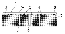
図1は本発明の一実施形態に係る真空吸着による基板載置装置、すなわち真空チャックの概略構成を示す断面図である。基板載置装置1は外周のリング状突起3の内側に、基板を載置する複数のピン状突起2、基板脱着用のリフトピン(図示せず)が上下できる貫通孔5、該貫通孔周囲のリング状突起4を有した構造を持ち、吸引穴6から真空排気することで、載置された基板を吸着固定することができる。これらの突起の高さは、ほぼ同一で、突起の先端は平面加工されており、この先端面、すなわち載置面に基板Wが載置される。
Hereinafter, the substrate mounting apparatus of the present invention will be described in more detail with reference to the drawings.
FIG. 1 is a cross-sectional view showing a schematic configuration of a substrate mounting apparatus by vacuum suction, that is, a vacuum chuck according to an embodiment of the present invention. The
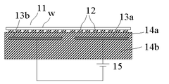
図2は、本発明の他の実施形態である静電吸着による基板載置装置11、すなわち静電チャックの概略構成を示す断面図である。セラミックス絶縁層14a及び同一のセラミックスからなる基台14bの間に1対の電極13a及び13bを内蔵し、電源15を接続した双極型構造の静電チャックである。絶縁層14aには基板を載置する複数のピン状突起12が形成されている。
FIG. 2 is a cross-sectional view showing a schematic configuration of a
なお、本発明は上記構造形態に限定されることなく種々変形可能である。例えば、突起の大きさ、高さ、数、および配置は限定されるものではなく任意に選択されて良い。例えば図1においては、突起2のみが載置面を形成し、リング状突起3、4は載置面を形成しない構造を採用でき、吸引穴の数、場所ともに図1に限定されるものではない。さらには、載置装置の外形も円形、四角形等、被吸着基板の形状に応じて選択されて良い。図2の静電チャックについても同様に、ピン状突起の他、リング状その他の突起を設けても良いし、真空吸着力を併用するための吸引穴を設けても良い。
In addition, this invention can be variously deformed without being limited to the said structure form. For example, the size, height, number, and arrangement of the protrusions are not limited and may be arbitrarily selected. For example, in FIG. 1, it is possible to adopt a structure in which only the
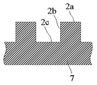
図3は、真空チャックの突起拡大断面図である。突起の先端面2aはRz0.5μm以下であり、側面2bおよび底面2cは先端面2aに対して、1.5〜3倍のRzを有した構造となっている。図3では、先端面、側面および底面を便宜的に全て直線で示したが、突起の角部や隅部は加工精度や突起の強度を考慮して適宜R形状等とすることができる。例えば突起の角部および隅部をR加工した場合、R部は側面または底面の一部とみなして表面粗さRzを測定して良い。なお、図3では、真空チャックの例を示したが、静電チャックにおいても同様の突起構造を有することは言うまでもない。
FIG. 3 is an enlarged sectional view of the protrusion of the vacuum chuck. The
突起の形状は、上述のようなピン形状の他、リング状、格子状、網状、またはこれらの組み合わせ等、特に限定しない。ただし、先に述べたように、基板と載置面の接触面積は小さいほうが良いので、ピン形状が最も望ましい。ピン形状は、角柱、円柱等種々の形状を採用でき、基板との接触面積を基板の面積の10%以下にすることが望ましい。 The shape of the protrusion is not particularly limited, such as the above-described pin shape, ring shape, lattice shape, mesh shape, or a combination thereof. However, as described above, since the contact area between the substrate and the mounting surface should be small, the pin shape is most desirable. As the pin shape, various shapes such as a prism and a cylinder can be adopted, and the contact area with the substrate is desirably 10% or less of the area of the substrate.
また、静電吸着による基板載置装置では、ピン状突起の総面積が小さくなると、基板に働く全体の吸着力が小さくなるが、吸着力は基板と接触している面だけでなく、非接触面部分でも発生する。この非接触面部分の吸着力は、突起の高さが低いほど大きくなるので、ピン状突起の基板との接触面積を小さくした場合でも、突起の高さを低くすれば、吸着力を確保することができる。また、ヒータ付き静電チャックの場合には、基板の温度分布の均一化を図るために、基板と静電チャック間にHeガスを流すことがある。このとき、He平均自由行程の観点から、突起高さを高くすると熱伝達効率がおちる。真空チャックの場合、突起が高いと基板とチャック間に乱流が発生しやすくなり、基板に付着するパーティクルの発生量が多くなる。以上を考えると、突起高さは50μm以下とすることが好ましい。また、突起高さは8μm以上とすることが好ましい。これは、突起高さが低すぎると底部との接触が起きるため、接触面積が増大するおそれがあるからである。 In addition, in the substrate mounting device by electrostatic adsorption, when the total area of the pin-shaped protrusions is reduced, the overall adsorption force acting on the substrate is reduced, but the adsorption force is not only in contact with the substrate but also in non-contact. It also occurs on the surface. Since the suction force of the non-contact surface portion increases as the height of the protrusion is lowered, even if the contact area of the pin-like protrusion with the substrate is reduced, the suction force is ensured by reducing the height of the protrusion. be able to. In the case of an electrostatic chuck with a heater, He gas may flow between the substrate and the electrostatic chuck in order to make the temperature distribution of the substrate uniform. At this time, from the viewpoint of the He mean free path, the heat transfer efficiency decreases when the height of the protrusion is increased. In the case of a vacuum chuck, if the protrusion is high, turbulent flow is likely to occur between the substrate and the chuck, and the amount of particles that adhere to the substrate increases. Considering the above, the height of the protrusion is preferably 50 μm or less. The protrusion height is preferably 8 μm or more. This is because if the height of the protrusion is too low, contact with the bottom portion occurs, which may increase the contact area.
セラミックス部材の主面に凹凸、すなわち突起を形成する方法としては特に限定せず、突起を形成する部分にマスクをして、それをブラスト加工する方法の他、エッチング処理したり、マシニングにより形成したりする方法が採用できる。 The method for forming irregularities, that is, protrusions, on the main surface of the ceramic member is not particularly limited. In addition to a method in which a mask is formed on the portion where the protrusion is to be formed and the surface is blasted, etching or machining is performed. Can be used.
本発明の基板載置装置に係るセラミックスは、相対密度が98%以上、気孔率は0.5%以下が望ましい。この範囲外では、範囲内に比べてパーティクルが発生し易くなるためである。したがって、相対密度はより大きいことが好ましく、気孔率もより小さいことが好ましい。 The ceramic according to the substrate mounting apparatus of the present invention preferably has a relative density of 98% or more and a porosity of 0.5% or less. This is because particles outside the range are more likely to generate particles than in the range. Accordingly, the relative density is preferably larger and the porosity is preferably smaller.
本発明の基板載置装置は、その処理環境に耐えることができる材質でなければならない。例えば、成膜処理やエッチング処理は、高温、腐食性ガス雰囲気で行われるために、このような用途に用いる基板載置装置には、耐熱性や耐食性に優れる材料であるセラミックスが用いられる。より具体的には、アルミナ、窒化アルミニウム、サイアロン、窒化珪素、炭化珪素、イットリアおよびイットリウムアルミニウムガーネット(YAG)の他、コーディエライト基セラミック、ユークリプタイト基セラミックおよびガラス質セラミック等の低熱膨張セラミック等が好適である。なお、真空吸着による基板載置装置においては、絶縁性、導電性を問わず、種々の材料を採用できるが、静電吸着による基板載置装置では、その使用温度において好適な体積抵抗率を備える材料を採用する必要がある。 The substrate mounting apparatus of the present invention must be made of a material that can withstand the processing environment. For example, since the film forming process and the etching process are performed in a high temperature and corrosive gas atmosphere, ceramics, which is a material having excellent heat resistance and corrosion resistance, is used for the substrate mounting apparatus used for such applications. More specifically, low thermal expansion ceramics such as alumina, aluminum nitride, sialon, silicon nitride, silicon carbide, yttria and yttrium aluminum garnet (YAG), cordierite-based ceramic, eucryptite-based ceramic, and glassy ceramic. Etc. are suitable. Note that various materials can be adopted for the substrate mounting device by vacuum suction regardless of insulation and conductivity, but the substrate mounting device by electrostatic suction has a suitable volume resistivity at its operating temperature. It is necessary to adopt materials.
また、凹凸を形成するセラミックス部材の主面以外の部分については、主面と同一のセラミックスであっても良いし、その他のセラミックス、金属、金属とセラミックスの複合材料等であっても良い。したがって、セラミックスの製造方法としては、常圧、ホットプレスのような焼結法の他、溶射、CVD、AD法等の周知の方法が採用できる。 Further, the portion other than the main surface of the ceramic member forming the irregularities may be the same ceramic as the main surface, or may be other ceramics, metal, a composite material of metal and ceramics, or the like. Therefore, as a method for producing ceramics, well-known methods such as thermal spraying, CVD, and AD methods can be adopted in addition to sintering methods such as normal pressure and hot pressing.
次に実施例として、真空チャック(試験例1〜10)および静電チャック(試験例11〜20)の試験例を示して本発明をさらに詳細に説明する。 Next, as examples, the present invention will be described in more detail by showing test examples of vacuum chucks (Test Examples 1 to 10) and electrostatic chucks (Test Examples 11 to 20).
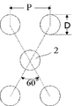
(試験例1〜10)炭化ケイ素粉末に炭化ホウ素0.4質量%、カーボン4質量%を添加した原料粉末を用いて10個の焼結体(φ210×10mm)を得た。アルキメデス法により算出した各焼結体の相対密度は、99%、気孔率は0.5%であった。これらの焼結体について円筒および平面研削を行い、φ200×8mmに加工し、中心に真空吸着のための直径1mmの貫通穴(吸引穴)を形成した。さらに載置面が形成される面について平面度が3μm以下となるようラップ加工を行った。次に載置面側に、図4に示すような、直径Dが0.5mm、間隔Pが2mm、千鳥60°のピンパターン、およびPCD198-200のリングパターンのマスクを貼り、ブラスト加工により高さ50μmのピン状突起およびリング状突起を形成した。これらの突起の先端面、側面および底面の研磨は、化学繊維製のクロス研磨盤を用い、磁性流体と砥粒を混合した研削液を用いて研磨を行った。しかる後に、突起の先端面について、研磨定盤を用いてラップ加工を施し、突起先端からなる平面の平面度を1μm以下に調整した。ただし、試験例10については、このラップ加工を行わず、クロス研磨盤を用いた研磨の後に次の工程に移行した。試験例10の突起先端からなる平面の平面度は4μmであった。これらの基板載置装置を洗浄した後、クラス100のクリーンルーム内でφ200mmシリコンウエハ吸着試験を行い、レーザー散乱方式の異物検査装置によりウエハのチャックに載置された面(ウエハ裏面)についてパーティクルサイズ0.2〜1.0μmのパーティクル測定を実施した。真空引きは基板載置装置の中心に形成した吸引穴から行い、ウエハを設置し-0.1MPaで1分間保持した。突起先端からなる平面の平面度は、φ200mmに入る全ての突起を対象としてレーザー干渉式形状測定機を用いて測定した。以下の試験例においても同様である。 (Test Examples 1 to 10) Ten sintered bodies (φ210 × 10 mm) were obtained using raw material powder obtained by adding 0.4% by mass of boron carbide and 4% by mass of carbon to silicon carbide powder. The relative density of each sintered body calculated by the Archimedes method was 99%, and the porosity was 0.5%. These sintered bodies were subjected to cylindrical and surface grinding, processed to φ200 × 8 mm, and a through hole (suction hole) having a diameter of 1 mm for vacuum suction was formed at the center. Further, lapping was performed so that the flatness of the surface on which the placement surface is formed is 3 μm or less. Next, as shown in FIG. 4, a mask having a pin pattern with a diameter D of 0.5 mm, a spacing P of 2 mm, a staggered 60 °, and a ring pattern of PCD198-200 as shown in FIG. A pin-shaped protrusion and a ring-shaped protrusion having a thickness of 50 μm were formed. The tip, side and bottom surfaces of these protrusions were polished by using a chemical fiber cloth polishing machine and using a grinding fluid mixed with magnetic fluid and abrasive grains. Thereafter, the tip surface of the protrusion was lapped using a polishing surface plate, and the flatness of the flat surface formed from the tip of the protrusion was adjusted to 1 μm or less. However, for Test Example 10, this lapping was not performed, and the process shifted to the next step after polishing using a cross polishing disk. The flatness of the flat surface composed of the tips of the protrusions in Test Example 10 was 4 μm. After cleaning these substrate placement devices, a φ200 mm silicon wafer adsorption test is performed in a class 100 clean room, and the particle size of the surface (wafer back surface) placed on the wafer chuck by the laser scattering type foreign matter inspection device is 0. Measurement of particles of 2 to 1.0 μm was performed. Vacuum drawing was performed from a suction hole formed at the center of the substrate mounting apparatus, and a wafer was placed and held at -0.1 MPa for 1 minute. The flatness of the flat surface composed of the tips of the protrusions was measured using a laser interference type shape measuring device for all protrusions having a diameter of 200 mm. The same applies to the following test examples.
(試験例11〜20)窒化アルミニウム粉末に酸化イットリウムを3質量%添加した原料粉末を用い、モリブデン製の双極型電極を埋設し焼成することで、φ210×10mmの10個の焼結体を得た。各焼結体の相対密度は99%、気孔率は0.5%であった。次にこの焼結体を円筒および平面研削を用い、絶縁層厚さが1mmに、外形をφ200×8mmに加工した。さらに載置面が形成される面について平面度が3μm以下となるようラップ加工を行った。次に絶縁層に上記試験例と同様に、直径Dが0.5mm、間隔Pが2mm、千鳥60°のピンパターンのマスクを貼り、ブラスト加工により高さ50μmのピン状突起を形成した。これらの突起の先端面、側面および底面の研磨は、化学繊維製のクロス研磨盤を用い、磁性流体と砥粒を混合した研削液を用いて研磨を行った。しかる後に、突起の先端面について、研磨定盤を用いたラップ加工を施し、突起先端からなる平面の平面度を1μm以下に調整した。ただし、試験例20については、このラップ加工を行わず、クロス研磨盤を用いた研磨の後に次の工程に移行した。試験例20の突起先端からなる平面の平面度は6μmであった。この基板載置装置を洗浄した後、クラス100クリーンルーム内で、500℃まで加熱し、双極型電極に1000V印加してφ200mmシリコンウエハを吸着させ、レーザー散乱方式の異物検査装置によりウエハのチャックに載置された面(ウエハ裏面)について0.2〜1.0μmサイズのパーティクル測定を実施した。 (Test Examples 11 to 20) Using a raw material powder obtained by adding 3% by mass of yttrium oxide to an aluminum nitride powder, by embedding and firing a molybdenum bipolar electrode, ten sintered bodies of φ210 × 10 mm were obtained. It was. Each sintered body had a relative density of 99% and a porosity of 0.5%. Next, this sintered body was processed into a thickness of 1 mm and an outer shape of φ200 × 8 mm using a cylinder and surface grinding. Further, lapping was performed so that the flatness of the surface on which the placement surface is formed is 3 μm or less. Next, in the same manner as in the above test example, a pin pattern mask having a diameter D of 0.5 mm, a spacing P of 2 mm, and a staggered 60 ° was pasted on the insulating layer, and pin-shaped protrusions having a height of 50 μm were formed by blasting. The tip, side and bottom surfaces of these projections were polished using a chemical fiber cloth polishing machine and using a grinding fluid mixed with magnetic fluid and abrasive grains. Thereafter, lapping using a polishing surface plate was performed on the tip surface of the protrusion, and the flatness of the flat surface composed of the tip of the protrusion was adjusted to 1 μm or less. However, for Test Example 20, this lapping was not performed, and the process shifted to the next step after polishing using a cross polishing disk. The flatness of the flat surface consisting of the tip of the protrusion of Test Example 20 was 6 μm. After cleaning this substrate mounting device, it is heated to 500 ° C. in a class 100 clean room, 1000V is applied to the bipolar electrode to adsorb a φ200 mm silicon wafer, and it is mounted on the wafer chuck by a laser scattering type foreign matter inspection device. Particles having a size of 0.2 to 1.0 μm were measured on the placed surface (wafer back surface).
表1に上記ウエハ吸着試験の結果を示す。突起先端面、側面及び底面のRzはJISB0601に基づいて粗さ測定機を用いて測定した。 Table 1 shows the results of the wafer adsorption test. Rz of the tip end face, side face and bottom face of the protrusion was measured using a roughness measuring machine based on JISB0601.

突起先端のRzの大きい真空チャックの試験例1および静電チャックの試験例11では、それぞれの装置のRzが小さい他の例に比べてパーティクルが多い結果となった。また、突起先端面のRzに対する突起側面および底面の表面粗さの比が1.5〜3の範囲外である試験例2、6および試験例12、16では、それぞれの装置で比較的パーティクルが多かった。さらに、平面度が大きい試験例10および20では、突起先端等のRzが小さいにも関わらずパーティクル数が多かった。一方、突起先端面のRzに対する突起側面および底面の表面粗さの比が上記範囲内である試験例では、いずれの装置においても範囲外に比べてパーティクル数が著しく少なかった。 In the test example 1 of the vacuum chuck having a large Rz at the tip of the protrusion and the test example 11 of the electrostatic chuck, the number of particles was larger than in other examples having a small Rz of each device. In Test Examples 2 and 6 and Test Examples 12 and 16 in which the ratio of the surface roughness of the protrusion side surface and the bottom surface to Rz of the protrusion front end surface is outside the range of 1.5 to 3, particles are relatively generated in each device. There were many. Furthermore, in Test Examples 10 and 20 having a high flatness, the number of particles was large despite the small Rz of the tip of the protrusion. On the other hand, in the test examples in which the ratio of the surface roughness of the protrusion side surface and the bottom surface to Rz of the protrusion front end face is within the above range, the number of particles was remarkably small in all apparatuses compared to the outside of the range.
1;真空吸着による基板載置装置
2;ピン状突起
2a;突起先端面
2b;側面
2c;底面
3、4;リング状突起
5;リフトピン貫通穴
6;吸引穴
11;静電吸着による基板載置装置
12;ピン状突起
13a、13b;双極型電極
14a;セラミックス絶縁層
14b;セラミックス基台
15;電源
W;基板
DESCRIPTION OF
Claims (4)
前記突起先端面の表面粗さ(最大高さ)Rzが0.5μm以下であって、
前記突起先端面のRzに対する突起側面および底面の表面粗さの比(側面および底面のRz/先端面のRz)が1.5〜3であることを特徴とする基板載置装置。 In the substrate mounting apparatus for mounting the substrate on the tip end surface of the protrusion,
The surface roughness (maximum height) Rz of the projection tip surface is 0.5 μm or less,
The substrate mounting apparatus, wherein a ratio of the surface roughness of the protrusion side surface and the bottom surface to Rz of the protrusion front surface (Rz of the side surface and bottom surface / Rz of the front surface) is 1.5 to 3.
平面研削された前記主面を研磨定盤によりラップ加工する工程と、
ラップ加工された前記主面に凹凸を形成する工程と、
前記凹凸の突起の先端面、側面および底面を溶媒に砥粒を分散させた研削液を用いて研磨する工程と、
前記突起の先端面を研磨定盤によりラップ加工する工程と、
を含むことを特徴とする請求項1、2記載の基板載置装置の製造方法。 A step of surface grinding the main surface of the ceramic member;
A step of lapping the principally ground surface with a polishing surface plate;
Forming irregularities on the lapped main surface;
Polishing the front surface, the side surface and the bottom surface of the projections of the irregularities using a grinding liquid in which abrasive grains are dispersed in a solvent;
Lapping the tip surface of the protrusion with a polishing surface plate;
The method for manufacturing a substrate mounting apparatus according to claim 1, wherein:
Priority Applications (1)
| Application Number | Priority Date | Filing Date | Title |
|---|---|---|---|
| JP2007129936A JP2008288288A (en) | 2007-05-16 | 2007-05-16 | Device for placing board |
Applications Claiming Priority (1)
| Application Number | Priority Date | Filing Date | Title |
|---|---|---|---|
| JP2007129936A JP2008288288A (en) | 2007-05-16 | 2007-05-16 | Device for placing board |
Publications (1)
| Publication Number | Publication Date |
|---|---|
| JP2008288288A true JP2008288288A (en) | 2008-11-27 |
Family
ID=40147751
Family Applications (1)
| Application Number | Title | Priority Date | Filing Date |
|---|---|---|---|
| JP2007129936A Pending JP2008288288A (en) | 2007-05-16 | 2007-05-16 | Device for placing board |
Country Status (1)
| Country | Link |
|---|---|
| JP (1) | JP2008288288A (en) |
Cited By (2)
| Publication number | Priority date | Publication date | Assignee | Title |
|---|---|---|---|---|
| JP2014027207A (en) * | 2012-07-30 | 2014-02-06 | Hitachi Chemical Co Ltd | Dielectric body and electrostatic chuck using the same |
| KR20210013762A (en) * | 2018-06-22 | 2021-02-05 | 어플라이드 머티어리얼스, 인코포레이티드 | Methods to minimize backside damage in semiconductor wafer processing |
-
2007
- 2007-05-16 JP JP2007129936A patent/JP2008288288A/en active Pending
Cited By (3)
| Publication number | Priority date | Publication date | Assignee | Title |
|---|---|---|---|---|
| JP2014027207A (en) * | 2012-07-30 | 2014-02-06 | Hitachi Chemical Co Ltd | Dielectric body and electrostatic chuck using the same |
| KR20210013762A (en) * | 2018-06-22 | 2021-02-05 | 어플라이드 머티어리얼스, 인코포레이티드 | Methods to minimize backside damage in semiconductor wafer processing |
| KR102862930B1 (en) * | 2018-06-22 | 2025-09-19 | 어플라이드 머티어리얼스, 인코포레이티드 | Methods for Minimizing Backside Damage in Semiconductor Wafer Processing |
Similar Documents
| Publication | Publication Date | Title |
|---|---|---|
| JP2008085129A (en) | Substrate mounting apparatus | |
| KR101142000B1 (en) | Electrostatic chuck | |
| JP5957812B2 (en) | Electrostatic chuck device | |
| TW571382B (en) | Electrostatic chuck and substrate processing apparatus | |
| WO2001013423A1 (en) | Semiconductor production device ceramic plate | |
| JP2006005095A (en) | Substrate heating apparatus and manufacturing method thereof | |
| JP4739039B2 (en) | Electrostatic chuck device | |
| JP2006049352A (en) | Suscepter apparatus | |
| KR20040030803A (en) | Ceramic connection body, method of connecting the ceramic bodies, and ceramic structural body | |
| JP7515583B2 (en) | Breathable plug, substrate support assembly and shower plate | |
| JPWO2014156619A1 (en) | Electrostatic chuck device | |
| CN103038874A (en) | Electrostatic chuck | |
| TWI785577B (en) | Air-permeable member, member for semiconductor manufacturing apparatus, plug and sucking member | |
| CN111918854A (en) | Ceramic substrate and susceptor | |
| JP2008004926A (en) | Wafer holder, manufacturing method thereof, and semiconductor manufacturing apparatus | |
| JP2001351966A (en) | Suscepter and method for manufacturing the suscepter | |
| JP5515365B2 (en) | Electrostatic chuck and method of manufacturing electrostatic chuck | |
| JP2003007682A (en) | Electrode member for plasma processing equipment | |
| JP4545536B2 (en) | Vacuum suction jig | |
| JP2008288288A (en) | Device for placing board | |
| KR102814219B1 (en) | Electrode-embedded member, substrate holding member, ceramic heater, and electrostatic chuck | |
| JP5011736B2 (en) | Electrostatic chuck device | |
| JP2007201068A (en) | Electrostatic chuck | |
| JP6017895B2 (en) | Alumina sintered body manufacturing method, vacuum chuck manufacturing method, and electrostatic chuck manufacturing method | |
| KR20050054950A (en) | Electrostatic chuck having a low level of particle generation and method of fabricating same |