JP2008257271A - Display device - Google Patents
Display device Download PDFInfo
- Publication number
- JP2008257271A JP2008257271A JP2008175358A JP2008175358A JP2008257271A JP 2008257271 A JP2008257271 A JP 2008257271A JP 2008175358 A JP2008175358 A JP 2008175358A JP 2008175358 A JP2008175358 A JP 2008175358A JP 2008257271 A JP2008257271 A JP 2008257271A
- Authority
- JP
- Japan
- Prior art keywords
- light emitting
- pixel
- video signal
- phosphorescent
- emitting pixel
- Prior art date
- Legal status (The legal status is an assumption and is not a legal conclusion. Google has not performed a legal analysis and makes no representation as to the accuracy of the status listed.)
- Pending
Links
- 239000000463 material Substances 0.000 claims abstract description 46
- 238000005401 electroluminescence Methods 0.000 claims description 4
- 239000010410 layer Substances 0.000 description 25
- 238000006243 chemical reaction Methods 0.000 description 24
- 238000003860 storage Methods 0.000 description 11
- 238000010586 diagram Methods 0.000 description 10
- 239000000758 substrate Substances 0.000 description 10
- 230000005281 excited state Effects 0.000 description 9
- 230000008033 biological extinction Effects 0.000 description 8
- 230000007704 transition Effects 0.000 description 8
- 239000003990 capacitor Substances 0.000 description 7
- 230000008859 change Effects 0.000 description 7
- 230000004044 response Effects 0.000 description 7
- 230000007423 decrease Effects 0.000 description 6
- 239000011159 matrix material Substances 0.000 description 6
- 238000010791 quenching Methods 0.000 description 6
- 230000000171 quenching effect Effects 0.000 description 6
- 239000000969 carrier Substances 0.000 description 5
- 230000005525 hole transport Effects 0.000 description 5
- 230000003287 optical effect Effects 0.000 description 5
- 239000010409 thin film Substances 0.000 description 5
- TVIVIEFSHFOWTE-UHFFFAOYSA-K tri(quinolin-8-yloxy)alumane Chemical compound [Al+3].C1=CN=C2C([O-])=CC=CC2=C1.C1=CN=C2C([O-])=CC=CC2=C1.C1=CN=C2C([O-])=CC=CC2=C1 TVIVIEFSHFOWTE-UHFFFAOYSA-K 0.000 description 5
- 230000003111 delayed effect Effects 0.000 description 4
- 238000000034 method Methods 0.000 description 4
- 239000000126 substance Substances 0.000 description 4
- VQGHOUODWALEFC-UHFFFAOYSA-N 2-phenylpyridine Chemical compound C1=CC=CC=C1C1=CC=CC=N1 VQGHOUODWALEFC-UHFFFAOYSA-N 0.000 description 3
- 230000006866 deterioration Effects 0.000 description 3
- 239000011521 glass Substances 0.000 description 3
- 239000012044 organic layer Substances 0.000 description 3
- 238000000059 patterning Methods 0.000 description 3
- 230000000630 rising effect Effects 0.000 description 3
- 230000032683 aging Effects 0.000 description 2
- 239000003086 colorant Substances 0.000 description 2
- 230000000694 effects Effects 0.000 description 2
- 230000005284 excitation Effects 0.000 description 2
- 230000006870 function Effects 0.000 description 2
- 230000005283 ground state Effects 0.000 description 2
- 230000020169 heat generation Effects 0.000 description 2
- 238000004519 manufacturing process Methods 0.000 description 2
- 230000007246 mechanism Effects 0.000 description 2
- 239000000203 mixture Substances 0.000 description 2
- OAICVXFJPJFONN-UHFFFAOYSA-N Phosphorus Chemical compound [P] OAICVXFJPJFONN-UHFFFAOYSA-N 0.000 description 1
- 230000000903 blocking effect Effects 0.000 description 1
- 230000010485 coping Effects 0.000 description 1
- 230000001934 delay Effects 0.000 description 1
- 230000018109 developmental process Effects 0.000 description 1
- 239000002019 doping agent Substances 0.000 description 1
- 238000002347 injection Methods 0.000 description 1
- 239000007924 injection Substances 0.000 description 1
- 239000002346 layers by function Substances 0.000 description 1
- 238000012423 maintenance Methods 0.000 description 1
- 230000014759 maintenance of location Effects 0.000 description 1
- 239000002184 metal Substances 0.000 description 1
- 230000008569 process Effects 0.000 description 1
- 230000006798 recombination Effects 0.000 description 1
- 238000005215 recombination Methods 0.000 description 1
Images


Landscapes
- Control Of El Displays (AREA)
- Electroluminescent Light Sources (AREA)
- Control Of Indicators Other Than Cathode Ray Tubes (AREA)
Abstract
Description
本発明は表示パネル、表示装置に係り、更に詳しくは有機エレクトロルミネッセンス素子(有機EL素子)より成る複数の画素が配された表示パネル、表示システムに関する。 The present invention relates to a display panel and a display device, and more particularly to a display panel and a display system in which a plurality of pixels each composed of an organic electroluminescence element (organic EL element) are arranged.
有機EL素子は、高輝度発光が可能な薄膜積層の面状の自発光を特徴とする。この有機EL素子は有機発光材料を含む発光層を少なくとも含む有機層の機能積層数を増やすことにより(非特許文献1及び非特許文献2)、低電圧で高効率な発光を可能としている。ここで基本となる素子構成は、陽極/正孔輸送層/発光層(有機発光材料を含む層)/陰極という構成でなりたっている。その後、陽極/正孔輸送層/発光層/電子輸送層/陰極の構成で更なる高効率化が図られてきた。また、発光層を通過するキャリアを阻止する為に発光層と電子輸送層の間にブロッキング層が設けられたり、低電圧でキャリアの注入が可能となるよう陰極と電子輸送層の間に電子注入層としての金属薄膜が設けられたりして、発光効率の改善が試みられてきた。
An organic EL element is characterized by planar self-luminous light emission of a thin film stack capable of high luminance light emission. This organic EL element enables high-efficiency light emission at a low voltage by increasing the number of functional layers of an organic layer including at least a light-emitting layer containing an organic light-emitting material (Non-Patent
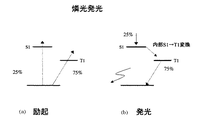
近年、電極から注入された電子、正孔の75%を形成する占有確率の高い3重項の励起子(残り、25%は1重項励起子を形成)からの発光を利用するIr錯体などの発光素子が注目されている(非特許文献3)。ここで1重項励起状態からの遷移による発光は蛍光を、3重項励起状態からの発光は燐光を用いている。 In recent years, Ir complexes that use light emitted from triplet excitons (the remaining 25% form singlet excitons) that form 75% of the electrons and holes injected from the electrodes have a high occupation probability. The light emitting element has attracted attention (Non-Patent Document 3). Here, light emission by transition from the singlet excited state uses fluorescence, and light emission from the triplet excited state uses phosphorescence.
例えば、下記の化1は、コダック(Kodak)社のシー ダブリュ タン(C.W.Tang)らによって開発された蛍光を主に用いたEL発光材料Alq3の分子図である。Alq3は緑色発光材料であり、1重項状態から蛍光を発光する。
For example, the following

一方、下記の(化2)はプリンストン(Prinston)のエム エイ バルド(M.A.Baldo)らによって開発されたIr(ppy)3の分子図である。Ir(ppy)3はAlq3と同様に緑色発光材料であるが、3重項状態から燐光を発光し、Alq3の数倍の効率を得ることが可能である。 On the other hand, the following (Chemical Formula 2) is a molecular diagram of Ir (ppy) 3 developed by M. A. Baldo et al. Of Princeton. Ir (ppy) 3 is a green light emitting material like Alq3, but emits phosphorescence from a triplet state and can obtain several times the efficiency of Alq3.
このような有機EL素子は、電極間の電流や薄膜トランジスタ(以下、TFTと略)からの電流により高輝度で面状に自発光するため、高密度な表示装置への利用が期待されている。また、赤、緑、青(RGB)を発光する有機EL素子を用いることにより、フルカラーの薄膜ディスプレイが実現できる。 Such an organic EL element is expected to be used for a high-density display device because it emits light in a planar state with high brightness due to a current between electrodes or a current from a thin film transistor (hereinafter abbreviated as TFT). In addition, a full-color thin film display can be realized by using organic EL elements that emit red, green, and blue (RGB).
従来の蛍光を用いた表示装置は素子の効率は低いが、消光時の応答速度は高速である。その消光遅延は、数十ns程度(Alq3:(化1)などの発光材料)のものがある。 A conventional display device using fluorescence has a low element efficiency, but has a high response speed during quenching. The extinction delay is about several tens of ns (Alq3: a light emitting material such as (Chemical Formula 1)).
一方で、燐光を用いて表示装置とした場合は効率は高いが、消光の遅延は約0.8μs〜数ms程度(Ir(ppy)3:(化2)などの発光材料)のものが知られている。 On the other hand, when a display device using phosphorescence is used, the efficiency is high, but the quenching delay is about 0.8 μs to several ms (light emitting material such as Ir (ppy) 3 : (Chemical Formula 2)). It has been.
また、蛍光発光材料と燐光発光材料とでは、その励起子のエネルギー遷移の仕方から初期の発光効率が両者で格段に違う場合がある。 In addition, there is a case where the initial light emission efficiency is significantly different between the fluorescent light emitting material and the phosphorescent light emitting material due to the energy transition of the exciton.
さらに、燐光による発光は、先ず、キャリアが一重項の最低励起状態、および、三重項の最低励起状態以上に励起される。この後、燐光発光では一重項の最低励起状態から三重項の最低励起状態に内部変換され、発光エネルギーを放出しながら基底状態へ戻ろうとする。一方で、蛍光による発光では、励起は燐光の場合と同様に行われるが、三重項の最低励起状態以上に励起されたキャリアはこのエネルギーを熱の形で放出する。このような発光メカニズムを鑑みるに、燐光による発光と、蛍光による発光は、分子間のエネルギー遷移が異なることによる発熱、形態変化からくる寿命の違いがある。 Further, in light emission by phosphorescence, first, carriers are excited above the singlet lowest excited state and the triplet lowest excited state. After that, in phosphorescence emission, the singlet lowest excited state is internally converted to the triplet lowest excited state, and it tries to return to the ground state while emitting light emission energy. On the other hand, in light emission by fluorescence, excitation is performed in the same manner as in the case of phosphorescence, but carriers excited above the triplet lowest excited state release this energy in the form of heat. In view of such a light emission mechanism, light emission by phosphorescence and light emission by fluorescence have a difference in lifetime due to heat generation and shape change due to different energy transitions between molecules.
このように蛍光発光材料と燐光発光材料とでは発光特性等が異なる等の理由から、複数の画素を配列する表示パネル上には、蛍光発光材料のみ、或いは燐光発光材料のみというように、全ての画素を同一の材料で構成し、高輝度、高表示品質のフルカラーの表示装置を目指した開発が盛んになされているが、このような表示装置においてはさらなる高性能化が求められていた。 As described above, for the reason that the fluorescent light emitting material and the phosphorescent light emitting material have different light emission characteristics, etc., on the display panel in which a plurality of pixels are arranged, all of the fluorescent light emitting material or only the phosphorescent light emitting material is used. Development has been actively made for a full-color display device with high luminance and high display quality in which pixels are made of the same material, but such a display device has been required to have higher performance.
本発明は、上記課題に鑑みなされたものであり、有機EL素子を利用し、より高輝度化、高表示品質化も可能な多色表示用の表示パネル、及びそれを用いた表示装置を提供することを目的とするものである。 The present invention has been made in view of the above problems, and provides a display panel for multicolor display that uses an organic EL element and can achieve higher luminance and higher display quality, and a display device using the display panel. It is intended to do.
多色表示、特にフルカラーの表示装置を構成する上では、色別の発光材料の効率の違いや視感度の違いからくる要求輝度等があるため、使用する材料を蛍光発光材料と燐光発光材料との両方から選択して用いることによって、より高輝度、高表示品質の表示が可能となることに本発明者らは着眼した。 In constructing a multicolor display, particularly a full-color display device, there are required luminance and the like due to the difference in efficiency of each luminescent material and the difference in visibility, so the materials to be used are a fluorescent luminescent material and a phosphorescent luminescent material. The present inventors have focused on the fact that display with higher luminance and higher display quality is possible by selecting and using both.
即ち、上記課題を解決するための第1の発明は、
一対の電極間に有機発光材料を含む発光層を少なくとも挟持した有機エレクトロルミネッセンス素子からなる画素が複数配列された表示パネルにおいて、
前記複数配列された画素が、主に蛍光発光材料を有機発光材料として用いた有機エレクトロルミネッセンス素子からなる蛍光発光画素と、主に燐光発光材料を有機発光材料として用いた有機エレクトロルミネッセンス素子からなる燐光発光画素と、を含むことを特徴とする表示パネルである。
That is, the first invention for solving the above problem is
In a display panel in which a plurality of pixels composed of an organic electroluminescence element in which at least a light emitting layer containing an organic light emitting material is sandwiched between a pair of electrodes,
The plurality of arranged pixels are mainly phosphorescent pixels composed of an organic electroluminescent element using a fluorescent light emitting material as an organic light emitting material, and phosphorescent composed mainly of an organic electroluminescent element using a phosphorescent light emitting material as an organic light emitting material. And a light emitting pixel.
本発明は、上記第1の発明において、
「蛍光発光画素のみを複数配列した第一表示部と、燐光発光画素のみを複数配列した第二表示部とを個別に有すること」、
「蛍光発光画素の面積が燐光発光画素の面積よりも大きいこと」、
更には、
「蛍光発光画素と燐光発光画素との面積の比が、該二つの画素の発光効率の比の逆比となっていること」、
をその好ましい態様として含むものである。
The present invention, in the first invention,
“Individually having a first display portion in which only a plurality of fluorescent light emitting pixels are arranged and a second display portion in which only a plurality of phosphorescent light emitting pixels are arranged”
"The area of the fluorescent pixel is larger than the area of the phosphorescent pixel",
Furthermore,
“The ratio of the area between the fluorescent light emitting pixel and the phosphorescent light emitting pixel is an inverse ratio of the ratio of the luminous efficiency of the two pixels.”
Is included as a preferred embodiment thereof.
上記課題を解決するための第2の発明は、
上記第1の発明に記載の表示パネルと、該表示パネルに信号を供給する制御手段とを備えた表示装置であって、
前記制御手段は、蛍光発光画素と燐光発光画素とで異なる信号を前記表示パネルに入力可能であることを特徴とする表示装置である。
The second invention for solving the above-mentioned problem is
A display device comprising: the display panel according to the first aspect of the present invention; and control means for supplying a signal to the display panel,
The control means is a display device characterized in that different signals can be input to the display panel between the fluorescent light emitting pixel and the phosphorescent light emitting pixel.
本発明は、上記第2の発明において、
「前記異なる信号においては、映像信号、及び/又は映像信号の対極の信号の立下りのタイミングが、燐光発光画素に入力する信号よりも蛍光発光画素に入力する信号の方が遅いこと」、
「前記制御手段が、蛍光発光画素と燐光発光画素との夫々の配置及び駆動条件を記憶する記憶手段を備えており、該記憶手段に記憶された記憶内容に基づいて、蛍光発光画素と燐光発光画素とで異なる発光特性に合わせて補正した信号を夫々の画素に入力可能であること」、
「補正する前記異なる発光特性として、発光効率を含むこと」、
「補正する前記異なる発光特性として、発光寿命を含むこと」、
をその好ましい態様として含むものである。
The present invention, in the second invention,
“In the different signals, the timing of the fall of the video signal and / or the opposite signal of the video signal is slower for the signal input to the fluorescent pixel than for the signal input to the phosphorescent pixel.”
“The control means includes storage means for storing the arrangement and driving conditions of the fluorescent light emitting pixel and the phosphorescent light emitting pixel, and the fluorescent light emitting pixel and the phosphorescent light emission are based on the stored contents stored in the storage means. The signal corrected according to the emission characteristics that differ from pixel to pixel can be input to each pixel. "
"Including the luminous efficiency as the different luminous characteristics to be corrected",
"Including the emission lifetime as the different emission characteristics to be corrected",
Is included as a preferred embodiment thereof.
本発明によれば、高効率の3重項材料を用いた燐光発光の素子と、従来、多数の材料が開発されている1重項材料を用いた蛍光発光の素子とを用いて、蛍光発光画素と燐光発光画素が混在した表示パネルや、同一の表示基板(ガラス基板,TFT基板)上に製造された、燐光発光素子のみで構成されるの第一表示部と燐光発光素子のみで構成される第二表示部との2種類の表示部からなる表示パネルにより、フルカラー等の多色表示用の表示パネルの高輝度化、高表示品質化が可能となる。 According to the present invention, phosphorescence emission using a phosphorescent light emitting element using a high-efficiency triplet material and a fluorescent light emitting element using a singlet material, for which many materials have been developed, are used. A display panel in which pixels and phosphorescent light-emitting pixels are mixed, or a first display unit made of only phosphorescent light-emitting elements manufactured on the same display substrate (glass substrate, TFT substrate) and a phosphorescent light-emitting element. The display panel composed of two types of display units, that is, the second display unit, can increase the brightness and display quality of a display panel for multicolor display such as full color.
また、このような表示パネルと、上記説明したような、信号立ち下がりタイミングをずらす機能、記憶手段に記憶された情報を基に発光効率の差や発光寿命の差を補正する機能を有する制御手段とを組み合わせた表示装置により、残光、初期表示ムラ、経時変化などを軽減した良好な階調表示が可能となる。なお、上記、映像信号変換メモリやコントローラは、表示パネルと同一基板上にあってもその作用効果は変らない。 Also, a control means having such a display panel, a function of shifting the signal fall timing as described above, and a function of correcting a difference in light emission efficiency and a light emission lifetime based on information stored in the storage means With the display device combined with the above, good gradation display with reduced afterglow, initial display unevenness, change with time, and the like can be achieved. Even if the video signal conversion memory and the controller are on the same substrate as the display panel, the operation and effects thereof are not changed.
以下、本発明の具体的な実施形態について図面を用いて説明しながら、本発明を詳細に説明する。 Hereinafter, the present invention will be described in detail while describing specific embodiments of the present invention with reference to the drawings.
図19、20は有機発光材料を含む発光層を少なくとも含む有機層を一対の電極である陽極および陰極で挟持した有機EL素子の典型的な構成を示す図であり、151はガラス基板、152はITOなどの透明な陽極、153は正孔輸送層、154は発光層、155は電子輸送層、156は陰極である。図20に示すように、陽極152側に正電圧、陰極156側に負電圧を印加することにより、正孔輸送層153を通った正孔158と電子輸送層155を通った電子159が発光層154で励起子を形成し、再結合により発光する。
19 and 20 are diagrams showing a typical configuration of an organic EL element in which an organic layer including at least a light emitting layer containing an organic light emitting material is sandwiched between an anode and a cathode as a pair of electrodes, 151 is a glass substrate, 152 is A transparent anode such as ITO, 153 is a hole transport layer, 154 is a light emitting layer, 155 is an electron transport layer, and 156 is a cathode. As shown in FIG. 20, when a positive voltage is applied to the
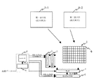
図1は本発明の表示装置の一実施形態を示すブロック図である。1は表示パネルを示しており、複数配列された画素9は、蛍光発光画素と燐光発光画素とを含んでいる。即ち、緑色の画素に用いられる有機EL素子の発光層は、主に1重項状態から蛍光を発光する蛍光発光材料より成る。また、赤色の画素には3重項状態から燐光を発光する燐光発光材料が用いられている。なお、燐光発光は、上記のように、蛍光発光の数倍の効率を得ることが可能である。そして、青色の画素には、緑色と同様に1重項状態から蛍光を発光する蛍光発光材料を用いた。これらの画素は表示装置の表示パネル部分に、図1に示されるようにマトリックス状に配置されている。ここで、表示パネル1の各絵素(RGB画素グループ)は、表示パネル1の部分拡大図となっている図3のように蛍光発光画素31,33と燐光発光画素32が混在している。
FIG. 1 is a block diagram showing an embodiment of a display device of the present invention.
従来、赤色の有機EL素子は高効率化が難しかったが、このように蛍光発光画素と燐光発光画素とから表示パネルを構成することにより、赤色の画素のみに燐光発光画素を用いて他の色との効率差を減少する等が可能となる。従って、例えばRGBによるフルカラー表示をする場合にも、三色の有機EL素子の輝度バランスを保ちながらも全画素の輝度を高く設定することができ、フルカラー等の多色表示用の表示パネルの高輝度化、高表示品質化が可能となる。 Conventionally, it has been difficult to increase the efficiency of red organic EL elements. However, by forming a display panel from fluorescent light emitting pixels and phosphorescent light emitting pixels in this way, phosphorescent light emitting pixels are used only for red pixels and other colors are used. It is possible to reduce the difference in efficiency. Therefore, for example, even in the case of full color display by RGB, the luminance of all pixels can be set high while maintaining the luminance balance of the three colors of organic EL elements, and the display panel for multicolor display such as full color can be set high. Brightness and high display quality can be achieved.
このように蛍光発光画素と燐光発光画素とを含む表示パネルを構成するには、同一基板上に、周知のパターニングを利用して蛍光発光画素と燐光発光画素とを混在させて形成する方法が挙げられるが、他にも、一枚の基板上には蛍光発光画素のみ、燐光発光画素のみの夫々を複数配列したものを2枚用意して第一表示部、第二表示部とし、これらを重ね合わせることで表示パネルを構成するといったことも可能である。但し、この場合には一方の表示部は、他方の表示部の発光が透過可能であるように、他方の表示部の画素の位置に対応する部分が透明である必要がある。第一表示部、第二表示部からなる構成によれば、パターニング等を用いて、蛍光発光画素又は燐光発光画素を形成した後に他方の画素を形成する場合に比べて工程を簡素化することが可能である。 In order to construct a display panel including fluorescent light emitting pixels and phosphorescent light emitting pixels in this way, a method of forming a mixture of fluorescent light emitting pixels and phosphorescent light emitting pixels on the same substrate by using well-known patterning can be cited. In addition, on the same substrate, two pieces of a plurality of arrangements of only fluorescent light emitting pixels and only phosphorescent light emitting pixels are prepared and used as a first display portion and a second display portion, and these are overlapped. A display panel can be configured by combining them. However, in this case, one display unit needs to be transparent at a portion corresponding to the pixel position of the other display unit so that the light emission of the other display unit can be transmitted. According to the configuration including the first display unit and the second display unit, the process can be simplified as compared with the case of forming the other pixel after forming the fluorescent pixel or the phosphorescent pixel by using patterning or the like. Is possible.
好ましくは、蛍光発光画素の面積が燐光発光画素の面積よりも大きいことである。上記のように、燐光発光は、蛍光発光の数倍の効率を得ることが可能であるため、燐光発光画素の方が単位面積当たりの輝度が大きい。そこで蛍光発光画素と燐光発光画素との面積をこのように変えることで、輝度差を減少することができる。さらに好ましくは、蛍光発光画素と燐光発光画素との面積の比が、該二つの画素の発光効率の比の逆比とすることである。これにより、輝度差をより小さくすることができる。なお、このように面積を異ならせる方法は、パターニング時に形成する有機層の面積を調節し、発光面積自体を異ならせる方法と、遮光部等を設けて開口面積を異ならせる方法とが挙げられる。 Preferably, the area of the fluorescent light emitting pixel is larger than the area of the phosphorescent light emitting pixel. As described above, phosphorescent light emission can obtain efficiency several times that of fluorescent light emission, and thus the phosphorescent pixel has higher luminance per unit area. Therefore, the luminance difference can be reduced by changing the areas of the fluorescent light emitting pixel and the phosphorescent light emitting pixel in this way. More preferably, the ratio of the area between the fluorescent light emitting pixel and the phosphorescent light emitting pixel is an inverse ratio of the ratio of the luminous efficiency of the two pixels. Thereby, a brightness | luminance difference can be made smaller. In addition, the method of making the areas different in this way includes a method of adjusting the area of the organic layer formed at the time of patterning to make the light emitting area itself different, and a method of making the opening area different by providing a light shielding portion or the like.
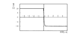
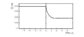
一方、これら蛍光発光画素と燐光発光画素との、映像信号電圧の立ち下がりに対する応答の波形は、図4乃至図6のようになっている。ここで、図5、図6のグラフの縦軸は光応答を測定するフォトマルチプライアの電圧出力となっている。図4のグラフの縦軸は各画素の立下りを測定するために用いた映像信号の電圧値である。燐光発光画素32の光学応答は図5に示されるように1μs程度であり、蛍光発光画素32の光学応答は図6に示されるように30〜40ns程度であるため、源信号遅れを加味しても燐光発光画素よりも蛍光発光画素の方が消光が早い。
On the other hand, the response waveforms of these fluorescent light emitting pixels and phosphorescent light emitting pixels with respect to the fall of the video signal voltage are as shown in FIGS. Here, the vertical axis of the graphs of FIGS. 5 and 6 represents the voltage output of the photomultiplier for measuring the optical response. The vertical axis of the graph in FIG. 4 represents the voltage value of the video signal used for measuring the fall of each pixel. The optical response of the
このように、表示信号に対して残光時間の違う画素が表示パネル1に混在することは、特定の表示色だけが浮かび上がって消光する原因となる。
As described above, the mixture of pixels having different afterglow times with respect to the display signal in the
また、図21、図22で示されるように、燐光による発光は、先ず、キャリアが一重項の最低励起状態S1、および、三重項の最低励起状態T1以上に励起される。この後、燐光発光ではS1からT1状態に内部変換され、発光エネルギーを放出しながら基底状態へ戻ろうとする。一方で、蛍光による発光では、励起は燐光の場合と同様に行われるが、T1状態以上に励起されたキャリアはこのエネルギーを熱の形で放出する。このような発光メカニズムを鑑みるに、燐光による発光と、蛍光による発光は、分子間のエネルギー遷移が異なることによる発熱、形態変化からくる寿命の違いがある。 In addition, as shown in FIGS. 21 and 22, light emission by phosphorescence is first excited to the singlet lowest excited state S1 and triplet lowest excited state T1 or more. Thereafter, phosphorescence emission is internally converted from the S1 state to the T1 state, and attempts to return to the ground state while emitting light emission energy. On the other hand, in the case of light emission by fluorescence, excitation is performed in the same manner as in the case of phosphorescence, but carriers excited to the T1 state or higher release this energy in the form of heat. In view of such a light emission mechanism, light emission by phosphorescence and light emission by fluorescence have a difference in lifetime due to heat generation and shape change due to different energy transitions between molecules.
従って、本発明においては、表示パネルに加えて、このように発光特性が異なる蛍光発光画素と燐光発光画素との夫々に異なる信号を入力可能である制御手段を備えた表示装置をも提供する。これにより、それぞれの発光特性に合わせて表示パネルに信号供給が可能となる。 Therefore, in addition to the display panel, the present invention also provides a display device including control means that can input different signals to the fluorescent light emitting pixels and the phosphorescent light emitting pixels having different light emission characteristics. Thereby, it is possible to supply a signal to the display panel in accordance with each light emission characteristic.
具体的には、先ず、映像信号、及び/又は映像信号の対極の信号の立下りのタイミングを、燐光発光画素に入力する信号よりも蛍光発光画素に入力する信号の方を遅くすることにより、上記の消光タイミングの違いによる特定色の残光を防止することができる。 Specifically, first, by delaying the timing of the fall of the video signal and / or the opposite signal of the video signal, the signal input to the fluorescent light emitting pixel than the signal input to the phosphorescent light emitting pixel, The afterglow of a specific color due to the difference in the extinction timing can be prevented.
さらに好ましくは、制御手段が、蛍光発光画素と燐光発光画素との夫々の配置及び駆動条件を記憶する記憶手段を備えており、該記憶手段に記憶された記憶内容に基づいて、蛍光発光画素と燐光発光画素とで異なる発光特性に合わせて補正した信号を夫々の画素に入力可能であることである。駆動条件とは、具体的には、駆動に用いる電圧値や、印加電圧の時系列波形等を指す。 More preferably, the control means includes storage means for storing the arrangement and driving conditions of each of the fluorescent light emitting pixel and the phosphorescent light emitting pixel, and based on the stored contents stored in the storage means, That is, it is possible to input a signal corrected in accordance with light emission characteristics different from those of phosphorescent light emitting pixels to each pixel. Specifically, the driving condition refers to a voltage value used for driving, a time series waveform of an applied voltage, or the like.
これにより、例えば蛍光発光画素と燐光発光画素との発光効率の違いを補正するために、記憶手段に記憶された配置及び駆動条件に基づいて、蛍光発光画素の方に高い電圧を印加し、発光効率に違いがあっても両者に輝度差が生じないようにすることができる。また、発光寿命の違いを補正するために、予め測定しておいた蛍光発光画素と燐光発光画素との一定時間後の発光効率の比を記憶手段に記憶しておき、これに合わせて一定時間後に印加する電圧値の比を決定することで、発光寿命の違いにより一定時間後における発光効率の比の変化にも対応することができ、長時間に渡って両者の輝度差の防止効果を持続することも可能となる。 Thus, for example, in order to correct the difference in luminous efficiency between the fluorescent light emitting pixel and the phosphorescent light emitting pixel, a higher voltage is applied to the fluorescent light emitting pixel based on the arrangement and driving conditions stored in the storage means, and the light emission Even if there is a difference in efficiency, it is possible to prevent a difference in luminance between the two. Further, in order to correct the difference in the light emission lifetime, the ratio of the luminous efficiency after a predetermined time between the fluorescent light emitting pixel and the phosphorescent light emitting pixel measured in advance is stored in the storage means, and in accordance with this, the predetermined time By determining the ratio of the voltage value to be applied later, it is possible to cope with the change in the ratio of the luminous efficiency after a certain time due to the difference in the light emission lifetime, and the effect of preventing the luminance difference between the two is maintained for a long time. It is also possible to do.
(実施の形態1)
まず図1に示した本発明の表示装置を、図9を合わせて参照しながら詳細に説明する。
(Embodiment 1)
First, the display device of the present invention shown in FIG. 1 will be described in detail with reference to FIG.
1は複数の画素9をマトリクス状に配置した表示パネルである。また、Vシフトレジスタ2、タイミング変換回路3、Hシフトレジスタ5、ラッチ4は、表示パネル1と同一面に設けられ、画素9に設けられた薄膜トランジスタ(以下、TFTと略)に映像信号、および、走査信号を供給する。本発明における制御手段は、図1においては表示パネル1以外の要素、即ち、Vシフトレジスタ2、タイミング変換回路3、Hシフトレジスタ5、ラッチ4、及びコントローラ7と映像信号変換メモリ(記憶手段)8とを含む表示制御部6に対応する。表示制御部6からはタイミング信号、および、映像信号が供給される。
画素9内の回路の一例を図9に示す。画素9内では、Pチャネル型のTFT93のソースが電源に、有機EL素子の陰極は接地電位に接続される。他方の陽極はTFT93のドレインに接続されている。また、Nチャネル型のTFT91のゲートは垂直走査の保持信号線に接続され、ソースは画像信号線に接続され、残りのドレイン線は保持容量92、および、TFT93のゲートに接続されている。画素の発光は、先ず、垂直走査の保持信号線を選択状態とし、画像信号線に水平ラッチ回路4にラッチされた映像信号が電圧として印加される。TFT91のソースとドレインは導通し、保持容量92が充電または放電される。そして、TFT93のゲート電位は、映像信号の電位に一致する。垂直走査の保持信号を非選択状態とすると、TFT91がオフとなる。このとき、TFT93は画像信号から切り離されるが、TFT93のゲートに接続された保持容量92により該電位は安定に保持される。こうして、TFT93のゲート、ソース間の保持容量92に応じた電流が有機EL素子94に供給される。
An example of a circuit in the pixel 9 is shown in FIG. In the pixel 9, the source of the P-channel TFT 93 is connected to the power source, and the cathode of the organic EL element is connected to the ground potential. The other anode is connected to the drain of the TFT 93. Further, the gate of the N-
図1の表示パネル1には、画素が正方状に配置され、図3に示されるように蛍光発光画素と燐光発光画素とが同一走査ラインに混在している。
In the
このような場合、同一走査ラインの各画素の消光時間は異なり、図16に示される消光時間の違いTd1が両画素間に生じる。 In such a case, the extinction time of each pixel on the same scanning line is different, and the difference Td1 in the extinction time shown in FIG. 16 occurs between the two pixels.
これを補正するために、図17に示されるように燐光発光の画素32の映像信号の立下り、即ち、水平ブランクHBLKへの信号切り換えを時間Td1だけ他の蛍光発光画素より早めている。
In order to correct this, as shown in FIG. 17, the fall of the video signal of the
図7には、上記、時間差を生じさせるための構成(タイミング変換回路3)の一実施形態が描かれている。ここで、n走査線保持信号は図1のVシフトレジスタ2より供給される。図7の画素73は燐光発光の画素であり、画素74は蛍光発光の画素である。各ライン毎に配置されたこれらの画素には、第一素子保持信号と第二素子保持信号の2種のタイミングの映像信号保持信号が与えられる。第一素子保持信号の立下りはフリップフロップ71,72で構成されたシフトレジスタにより、該信号が図17のTd1だけ遅らされている(時間はフリップフロップの段数とHシフトクロックの周期で決めることができる)。第一素子保持信号と第二素子保持信号の立ち上がりは、図示しない水平ブランクの生成に合わせて、図17のように一致させられる。
FIG. 7 shows an embodiment of the above-described configuration (timing conversion circuit 3) for generating a time difference. Here, the n scanning line holding signal is supplied from the
次に初期の発光効率の違いを補正する部分を説明する。 Next, the part which corrects the difference in the initial luminous efficiency will be described.
蛍光による発光画素31,33と燐光による発光画素32では、前述のように内部のエネルギー遷移が異なるので、初期の発光効率が著しく異なる。
The
両者の発光比を視感度比に揃えるために、表示制御部6の映像信号変換メモリ8により、映像信号の電圧を燐光発光画素32と蛍光発光画素31,33で倍率を変えて水平映像信号ラッチ4へ供給する。図11には、この映像信号変換メモリの内容が示されている。ここでは、表示パネル1の画素マトリクスは12×7で構成されている。燐光発光材料の発光効率は、蛍光発光材料の発光効率の3倍が理論値として知られている。これにより、図11においては燐光発光画素32の発光効率と蛍光発光画素31,33の倍率比は1:3に指定された好ましい形態が示されているが、この限りではない。
In order to make the light emission ratio of the two equal to the visibility ratio, the video
図11の映像信号の倍率は図12に示されるように映像信号と一緒に読み出され、映像信号が乗算で所定の倍率にされて水平映像信号ラッチ4へ供給される。水平映像信号ラッチ4でラッチされた映像信号は、上述したようにVシフトレジスタ2のタイミングにより、画素内TFT93から発光素子94へ電流として供給される。これにより、発光効率の異なる蛍光発光画素と燐光発光画素とを用いた表示装置の初期表示を視感度上略均一としている。なお、これらの画素の発光輝度は、その面積比を変えることで、視感度上略均一にすることもできる。
The magnification of the video signal in FIG. 11 is read together with the video signal as shown in FIG. 12, and the video signal is multiplied to a predetermined magnification and supplied to the horizontal
有機EL素子は経時とともに電流に対する発光輝度が落ちてくることが知られている。上述のように、この劣化も燐光発光画素32と蛍光発光画素31,33では輝度の落ち方が異なった傾向を示す。図13には、これに対応するための映像信号変換メモリの内容が示されている。ここでは、表示パネル1の画素マトリクスは12×7で構成されている。
It is known that the luminance of light emission with respect to current decreases with time in organic EL elements. As described above, this deterioration also shows a tendency in which the luminance decreases in the phosphorescent
初期の段階では図11のように、燐光発光画素32の発光効率と蛍光発光画素31,33の倍率比は1:3に指定されている。そして1000時間後の図13の映像信号の倍率は、燐光発光画素32の発光効率と蛍光発光画素31,33の倍率比は1:2に指定されている。この映像信号変換メモリ8の書き換えは、コントローラ7の計時により1000時間カウント後、初期に設定された変化率に応じてメモリの書き換えをおこなう。なお、倍率比は1:2は、燐光発光画素の方が蛍光発光画素より早く劣化したことによる。これらの倍率は、図12に示されるように映像信号と一緒に順次読み出されて、乗算器84で映像信号は所定の倍率にされて水平映像信号ラッチ4へ供給される。水平映像信号ラッチ4でラッチされた映像信号は、上述したようにVシフトレジスタ2のタイミングにより、画素内TFT93から有機EL素子94へ電流として供給される。これにより、発光寿命の異なる蛍光発光画素と燐光発光画素とを用いた表示装置の経時後の表示を視感度上略均一としている。
At the initial stage, as shown in FIG. 11, the luminous efficiency of the phosphorescent
(実施の形態2)
本形態も、実施形態1の図1に示される形態とほとんど同様であるが、本形態においては、図15に示されるように蛍光発光画素32と燐光発光画素33が別々の走査ラインに分かれて表示パネル1に混在している。
(Embodiment 2)
This embodiment is also almost the same as the embodiment shown in FIG. 1 of the first embodiment, but in this embodiment, as shown in FIG. 15, the
このような場合、走査ライン毎の画素の消光時間が異なり、図16に示される消光時間の違いTd1が該両素に生じる。 In such a case, the extinction time of the pixels for each scanning line is different, and the difference Td1 in the extinction time shown in FIG.
これを補正するために、図18の燐光の消光の立下り時間の遅延Td1を面積で換算した分の時間分Td2を図17のTd1として、即ち、水平ブランクHBLKへの信号切り換えを時間Td1だけ燐光発光画素の立ち下がりを蛍光発光画素より早めている。 In order to correct this, the time Td2 corresponding to the area obtained by converting the delay Td1 of the phosphorescence quenching time in FIG. 18 into Td1 is set as Td1 in FIG. 17, that is, the signal switching to the horizontal blank HBLK is performed only for time Td1. The fall of the phosphorescent light emitting pixel is earlier than that of the fluorescent light emitting pixel.
図8には、上記、時間差を生じさせるための構成の一実施形態が描かれている。ここで、n走査線保持信号は図1のVシフトレジスタ2より供給される。図8の画素73は燐光発光画素であり、画素74は蛍光発光画素である。各ライン毎に配置されたこれらの画素には、第一素子保持信号と第二素子保持信号の2種のタイミングの映像信号保持信号が与えられる。第一素子保持信号の立下りは、抵抗81と容量82で時定数を設定することにより該信号が図17のTd1だけ遅らされている(時間は抵抗81と容量82値で決めることができる)。第一素子保持信号と第二素子保持信号の立ち上がりは、図示しない水平ブランクの生成に合わせて、図17のように一致させられる。
FIG. 8 illustrates an embodiment of the configuration for generating the time difference. Here, the n scanning line holding signal is supplied from the
次に初期の発光効率の違いを補正する部分を説明する。 Next, the part which corrects the difference in the initial luminous efficiency will be described.
蛍光発光画素33と燐光発光画素32では、前述のように内部のエネルギー遷移が異なるので、初期の発光効率が著しく異なる。
Since the internal energy transition is different between the fluorescent
両者の発光比を視感度比に揃えるために、表示制御部6の映像信号変換メモリ8により、映像信号の電圧を燐光発光画素32と蛍光発光画素33で倍率を変えて水平映像信号ラッチ4へ供給する。図14には、この映像信号変換メモリの内容が示されている。ここでは、表示パネル1の画素マトリクスは12×8で構成されている(不図示)。燐光発光材料の発光効率は、蛍光発光材料の発光効率の3倍が理論値として知られている。これにより、燐光発光画素32の発光効率と蛍光発光画素33の倍率比は1:3に指定された好ましい形態が示されているが、この限りではない。
In order to make the both emission ratios equal to the visibility ratio, the video
図14の映像信号の倍率は走査線毎に映像信号と一緒に読み出され、映像信号が乗算で所定の倍率にされて水平映像信号ラッチ4へ供給される。水平映像信号ラッチ4でラッチされた映像信号は、上述したようにVシフトレジスタ2のタイミングにより、画素内TFT93から有機EL素子94へ電流として供給される。例えば、図15の一重項発光素子よりなる走査線33には、図14の3の倍率が映像信号に乗算された信号が供給されることになる。次の三重項発光素子よりなる走査線32には、図14の1の倍率が映像信号に乗算された信号が供給されることになる。これにより、発光効率の異なる蛍光発光画素と燐光発光画素とを用いた表示装置の初期表示を視感度上略均一としている。これらの画素の発光輝度は、その面積比を変えることでも視感度上略均一にすることができる。
The magnification of the video signal in FIG. 14 is read together with the video signal for each scanning line, and the video signal is multiplied to a predetermined magnification and supplied to the horizontal
有機EL素子は経時とともに電流に対する発光輝度が落ちてくることが知られている。上述のように、この劣化も燐光発光画素32と蛍光発光画素33では輝度の落ち方が異なった傾向を示す。初期の段階では図14のように、燐光発光画素32の発光効率と蛍光発光画素33の倍率比は1:3に指定されている。1000時間後の映像信号の倍率は、燐光発光画素32の発光効率と蛍光発光画素33の倍率比を1:2に映像信号変換メモリ8へ指定し直す。この映像信号変換メモリ8の書き換えは、コントローラ7の計時により1000時間カウント後、初期に設定された変化率に応じてメモリの書き換えをおこなう。なお、倍率比1:2は、燐光発光画素の方が蛍光発光画素より早く劣化したことによる。1:2に書き換えられた図14の映像信号の倍率は走査線毎に映像信号と一緒に読み出され、映像信号が乗算で所定の倍率にされて水平映像信号ラッチ4へ供給される。水平映像信号ラッチ4でラッチされた映像信号は、上述したようにVシフトレジスタ2のタイミングにより、画素内TFT93から有機EL素子94へ電流として供給される。これにより、発光寿命の異なる蛍光発光画素と燐光発光画素とを用いた表示装置の経時後の表示を視感度上略均一としている。
It is known that the luminance of light emission with respect to current decreases with time in organic EL elements. As described above, this deterioration also shows a tendency in which the luminance decreases in the phosphorescent
(実施の形態3)
本形態においては、図2に示すように、蛍光発光画素のみを複数配列した第一表示部と、燐光発光画素のみを複数配列した第二表示部とを個別に有し、これらを重ね合わせて表示パネル1を構成している。即ち、一方は、蛍光発光をなす一重項材料が図9に示すTFTを多数配置した基板上に蒸着されている。他方は、燐光発光をなす三重項材料が図9に示すTFTを多数配置した基板上に蒸着されている。
(Embodiment 3)
In this embodiment, as shown in FIG. 2, the first display unit in which only a plurality of fluorescent light emitting pixels are arranged and the second display unit in which only a plurality of phosphorescent light emitting pixels are arranged are individually provided, and these are overlapped. A
これらの表示部の消光時間は異なり、図16に示される消光時間の違いTd1が該両表示部間に生じる。 The extinction times of these display portions are different, and the difference Td1 in the extinction time shown in FIG. 16 occurs between the two display portions.
これを補正するために、図17に示されるように蛍光発光の第一表示部1−1を用いたときの映像信号の立下り、即ち、水平ブランクHBLKへの信号切り換えを時間Td1だけ燐光発光の第二表示部1−2を用いるときより遅くしている。 In order to correct this, as shown in FIG. 17, when the first display unit 1-1 for fluorescence emission is used, the fall of the video signal, that is, the signal switching to the horizontal blank HBLK is phosphorescent emission for the time Td1. It is later than when using the second display part 1-2.
使用する表示部毎に第一素子保持信号と第二素子保持信号の2種のタイミングのどちらかが映像信号保持信号として与えられる。これらの保持信号の生成には図7に示された時間差を生じさせるための構成を用いる。走査線保持信号は図1のVシフトレジスタ2より供給される。第二表示部1−2を用いるときは信号の立下りが遅延しない第二素子保持信号を用いる。また、第一表示部1−1を用いるときはTd1だけ遅らされている第一素子保持信号を用いる。第一素子保持信号の立下りはフリップフロップ71,72で構成されたシフトレジスタによりTd1だけ遅らされている(時間はフリップフロップの段数とHシフトクロックの周期で決めることができる)。第一素子保持信号と第二素子保持信号の立ち上がりは、図示しない水平ブランクの生成に合わせて図17のように一致させられる。
One of the two timings of the first element holding signal and the second element holding signal is given as the video signal holding signal for each display unit to be used. The generation of these holding signals uses the configuration for generating the time difference shown in FIG. The scanning line holding signal is supplied from the
これらの遅延は図8に示すように、抵抗81と容量82で時定数を設定することでも実現できる。
These delays can also be realized by setting a time constant with a
次に初期の発光効率の違いを補正する部分を説明する。 Next, the part which corrects the difference in the initial luminous efficiency will be described.
蛍光による第一表示部1−1と燐光による第二表示部1−2では、前述のように内部のエネルギー遷移が異なるので、初期の発光効率が著しく異なる。 Since the internal energy transition is different between the first display unit 1-1 by fluorescence and the second display unit 1-2 by phosphorescence as described above, the initial luminous efficiency is significantly different.
それぞれ用いる表示部により発光比を視感度比に揃えるために、表示制御部6の映像信号変換メモリ8により、映像信号の電圧を蛍光発光を用いた第一表示部1−1と燐光発光を用いた第二表示部1−2で倍率を変えて水平映像信号ラッチ4へ供給する。図14には、この表示部へ適用するための映像信号変換メモリの内容が示されている。燐光発光材料の発光効率は、蛍光発光材料の発光効率の3倍が理論値として知られている。これにより、蛍光発光の第一表示部1−1と燐光発光の第二表示部1−2を用いる場合の倍率比は3:1に指定されている。しかしながら、燐光材料の内部エネルギー遷移状態やドーパント濃度による消光などで効率は変るため、倍率比はこの限りでない。
In order to align the light emission ratio with the visibility ratio by the display units used, the video
図14の映像信号の倍率は走査線毎に映像信号と一緒に読み出され、映像信号が乗算で所定の倍率にされて水平映像信号ラッチ4へ供給される。水平映像信号ラッチ4でラッチされた映像信号は、上述したようにVシフトレジスタ2のタイミングにより、画素内TFT93から有機EL素子94へ電流として供給される。例えば、図15の一重項発光素子よりなる走査線33には、図14の3の倍率が映像信号に乗算された信号が供給されることになる。次の三重項発光素子よりなる走査線32には、図14の1の倍率が映像信号に乗算された信号が供給されることになる。これにより、発光効率の異なる蛍光発光画素と燐光発光画素とを用いた夫々の表示部の初期表示を視感度上略均一としている。
The magnification of the video signal in FIG. 14 is read together with the video signal for each scanning line, and the video signal is multiplied to a predetermined magnification and supplied to the horizontal
有機EL素子は経時とともに電流に対する発光輝度が落ちてくることが知られている。上述のように、この劣化も燐光発光画素32と蛍光発光画素33では輝度の落ち方が異なった傾向を示す。ここでは、表示パネル1の画素マトリクスは12×8で構成されている。初期の段階では図14のように、燐光発光画素32の発光効率と蛍光発光画素33の倍率比は1:3に指定されている。1000時間後の映像信号の倍率は、燐光発光画素32の発光効率と蛍光発光画素33の倍率比を1:2に映像信号変換メモリ8へ指定し直す。この映像信号変換メモリ8の書き換えは、コントローラ7の計時により1000時間カウント後、初期に設定された変化率に応じてメモリの書き換えをおこなう。なお、倍率比は1:2は、燐光発光画素の方が蛍光発光画素より早く劣化したことによる。1:2に書き換えられた図14の映像信号の倍率(不図示)は走査線毎に映像信号と一緒に読み出され、映像信号が乗算で所定の倍率にされて水平映像信号ラッチ4へ供給される。水平映像信号ラッチ4でラッチされた映像信号は、上述したようにVシフトレジスタ2のタイミングにより、画素内TFT93から有機EL素子94へ電流として供給される。これにより、発光寿命の異なる第一表示部1−1と第二表示部1−2とを用いた表示装置の経時後の表示を視感度上略均一としている。
It is known that the luminance of light emission with respect to current decreases with time in organic EL elements. As described above, this deterioration also shows a tendency in which the luminance decreases in the phosphorescent
1 表示パネル
1−1 第一表示部
1−2 第二表示部
2 Vシフトレジスタ
3 タイミング変換回路
4 ラッチ
5 Hシフトレジスタ
6 表示制御部
7 コントローラ
8 映像信号変換メモリ(記憶手段)
9 画素
31 蛍光発光画素(G)
32 燐光発光画素(R)
33 蛍光発光画素(B)
71 フリップフロップ
72 フリップフロップ
73 燐光発光画素
74 蛍光発光画素
81 抵抗
82 容量
84 乗算器
85 画素倍率
86 画素倍率
87 画素倍率
91 TFT
92 保持容量
93 TFT
94 有機EL素子
151 ガラス基板
152 陽極
153 正孔輸送層
154 発光層
155 電子輸送層
156 陰極
157 電源
158 正孔
159 電子
DESCRIPTION OF
9
32 Phosphorescent light emitting pixel (R)
33 Fluorescent pixels (B)
71 Flip-
92 Retention capacity 93 TFT
94
Claims (5)
前記複数配列された画素が、蛍光発光画素と、燐光発光画素と、を含み、
前記制御手段は、前記蛍光発光画素と、前記燐光発光画素とで異なる保持信号を前記表示パネルに入力可能であることを特徴とする表示装置。 A display panel in which a plurality of pixels each made of an organic electroluminescence element having at least a light emitting layer containing an organic light emitting material interposed between a pair of electrodes is arranged, and a control means for supplying a holding signal and a video signal to the display panel. In the display device,
The plurality of arranged pixels includes a fluorescent light emitting pixel and a phosphorescent light emitting pixel,
The display device is characterized in that the control means can input different holding signals to the display panel between the fluorescent light emitting pixel and the phosphorescent light emitting pixel.
前記複数配列された画素が、蛍光発光画素と、燐光発光画素と、を含み、
蛍光発光画素に接続されている前記走査線と、前記燐光発光画素に接続されている前記走査線とが異なることを特徴とする表示装置。 A display panel in which a plurality of pixels each made of an organic electroluminescence element having at least a light emitting layer containing an organic light emitting material sandwiched between a pair of electrodes, and a control means for supplying a holding signal to the display panel via a scanning line In the provided display device,
The plurality of arranged pixels includes a fluorescent light emitting pixel and a phosphorescent light emitting pixel,
The display device, wherein the scanning line connected to the fluorescent light emitting pixel is different from the scanning line connected to the phosphorescent light emitting pixel.
Priority Applications (1)
| Application Number | Priority Date | Filing Date | Title |
|---|---|---|---|
| JP2008175358A JP2008257271A (en) | 2008-07-04 | 2008-07-04 | Display device |
Applications Claiming Priority (1)
| Application Number | Priority Date | Filing Date | Title |
|---|---|---|---|
| JP2008175358A JP2008257271A (en) | 2008-07-04 | 2008-07-04 | Display device |
Related Parent Applications (1)
| Application Number | Title | Priority Date | Filing Date |
|---|---|---|---|
| JP2002159000A Division JP4217428B2 (en) | 2002-05-31 | 2002-05-31 | Display device |
Publications (2)
| Publication Number | Publication Date |
|---|---|
| JP2008257271A true JP2008257271A (en) | 2008-10-23 |
| JP2008257271A5 JP2008257271A5 (en) | 2008-12-04 |
Family
ID=39980815
Family Applications (1)
| Application Number | Title | Priority Date | Filing Date |
|---|---|---|---|
| JP2008175358A Pending JP2008257271A (en) | 2008-07-04 | 2008-07-04 | Display device |
Country Status (1)
| Country | Link |
|---|---|
| JP (1) | JP2008257271A (en) |
Cited By (4)
| Publication number | Priority date | Publication date | Assignee | Title |
|---|---|---|---|---|
| CN103229596A (en) * | 2010-12-20 | 2013-07-31 | 松下电器产业株式会社 | Organic electroluminescence (EL) display panel and method for manufacturing same |
| JP2013254941A (en) * | 2012-05-09 | 2013-12-19 | Semiconductor Energy Lab Co Ltd | Display device, and electronic apparatus |
| JP2021012365A (en) * | 2019-07-03 | 2021-02-04 | エルジー ディスプレイ カンパニー リミテッド | Display device, gate driver circuit, and driving method |
| US11355069B2 (en) | 2019-07-03 | 2022-06-07 | Lg Display Co., Ltd. | Display device, gate driving circuit, and driving method thereof |
Citations (14)
| Publication number | Priority date | Publication date | Assignee | Title |
|---|---|---|---|---|
| JPH11259044A (en) * | 1997-12-15 | 1999-09-24 | Thomson Multimedia Sa | Method for compensating difference between afterglow properties of phosphor in picture display screen and device therefor |
| JP2000252063A (en) * | 1999-03-01 | 2000-09-14 | Toppan Printing Co Ltd | Color switching light emitting element, substrate for the same, and color display device |
| JP2001142427A (en) * | 1999-11-16 | 2001-05-25 | Pioneer Electronic Corp | Matrix type display device and its driving method |
| JP2001236034A (en) * | 2000-02-22 | 2001-08-31 | Sharp Corp | Display device |
| JP2001255507A (en) * | 2000-03-13 | 2001-09-21 | Ichikoh Ind Ltd | Backlight for color liquid crystal display device |
| JP2001290441A (en) * | 1999-02-26 | 2001-10-19 | Sanyo Electric Co Ltd | Color display device |
| JP2001345177A (en) * | 2000-03-06 | 2001-12-14 | Semiconductor Energy Lab Co Ltd | Thin film forming device, thin film forming method therefor and spontaneous light emitting device |
| JP2001345176A (en) * | 2000-02-28 | 2001-12-14 | Semiconductor Energy Lab Co Ltd | Thin film forming device, thin film forming method therefor and spontaneous light emitting device |
| JP2002032051A (en) * | 2000-07-18 | 2002-01-31 | Sony Corp | Display device and its driving method, and portable terminal |
| JP2002062824A (en) * | 2000-06-05 | 2002-02-28 | Semiconductor Energy Lab Co Ltd | Light emitting device |
| JP2002072208A (en) * | 2000-06-15 | 2002-03-12 | Sharp Corp | Liquid crystal display device, method of driving the same and illuminator |
| JP2002151269A (en) * | 2000-08-28 | 2002-05-24 | Semiconductor Energy Lab Co Ltd | Light-emitting device |
| JP2003173154A (en) * | 2001-09-28 | 2003-06-20 | Sanyo Electric Co Ltd | Semiconductor device and display device |
| JP2003223137A (en) * | 2002-01-31 | 2003-08-08 | Hitachi Ltd | Display device and its driving method |
-
2008
- 2008-07-04 JP JP2008175358A patent/JP2008257271A/en active Pending
Patent Citations (14)
| Publication number | Priority date | Publication date | Assignee | Title |
|---|---|---|---|---|
| JPH11259044A (en) * | 1997-12-15 | 1999-09-24 | Thomson Multimedia Sa | Method for compensating difference between afterglow properties of phosphor in picture display screen and device therefor |
| JP2001290441A (en) * | 1999-02-26 | 2001-10-19 | Sanyo Electric Co Ltd | Color display device |
| JP2000252063A (en) * | 1999-03-01 | 2000-09-14 | Toppan Printing Co Ltd | Color switching light emitting element, substrate for the same, and color display device |
| JP2001142427A (en) * | 1999-11-16 | 2001-05-25 | Pioneer Electronic Corp | Matrix type display device and its driving method |
| JP2001236034A (en) * | 2000-02-22 | 2001-08-31 | Sharp Corp | Display device |
| JP2001345176A (en) * | 2000-02-28 | 2001-12-14 | Semiconductor Energy Lab Co Ltd | Thin film forming device, thin film forming method therefor and spontaneous light emitting device |
| JP2001345177A (en) * | 2000-03-06 | 2001-12-14 | Semiconductor Energy Lab Co Ltd | Thin film forming device, thin film forming method therefor and spontaneous light emitting device |
| JP2001255507A (en) * | 2000-03-13 | 2001-09-21 | Ichikoh Ind Ltd | Backlight for color liquid crystal display device |
| JP2002062824A (en) * | 2000-06-05 | 2002-02-28 | Semiconductor Energy Lab Co Ltd | Light emitting device |
| JP2002072208A (en) * | 2000-06-15 | 2002-03-12 | Sharp Corp | Liquid crystal display device, method of driving the same and illuminator |
| JP2002032051A (en) * | 2000-07-18 | 2002-01-31 | Sony Corp | Display device and its driving method, and portable terminal |
| JP2002151269A (en) * | 2000-08-28 | 2002-05-24 | Semiconductor Energy Lab Co Ltd | Light-emitting device |
| JP2003173154A (en) * | 2001-09-28 | 2003-06-20 | Sanyo Electric Co Ltd | Semiconductor device and display device |
| JP2003223137A (en) * | 2002-01-31 | 2003-08-08 | Hitachi Ltd | Display device and its driving method |
Cited By (8)
| Publication number | Priority date | Publication date | Assignee | Title |
|---|---|---|---|---|
| CN103229596A (en) * | 2010-12-20 | 2013-07-31 | 松下电器产业株式会社 | Organic electroluminescence (EL) display panel and method for manufacturing same |
| JP2013254941A (en) * | 2012-05-09 | 2013-12-19 | Semiconductor Energy Lab Co Ltd | Display device, and electronic apparatus |
| TWI611215B (en) * | 2012-05-09 | 2018-01-11 | 半導體能源研究所股份有限公司 | Display device and electronic device |
| US10042174B2 (en) | 2012-05-09 | 2018-08-07 | Semiconductor Energy Laboratory Co., Ltd. | Display device and electronic device |
| US10416466B2 (en) | 2012-05-09 | 2019-09-17 | Semiconductor Energy Laboratory Co., Ltd. | Display device and electronic device |
| JP2021012365A (en) * | 2019-07-03 | 2021-02-04 | エルジー ディスプレイ カンパニー リミテッド | Display device, gate driver circuit, and driving method |
| US11355069B2 (en) | 2019-07-03 | 2022-06-07 | Lg Display Co., Ltd. | Display device, gate driving circuit, and driving method thereof |
| JP7085587B2 (en) | 2019-07-03 | 2022-06-16 | エルジー ディスプレイ カンパニー リミテッド | Display device, gate drive circuit, and drive method |
Similar Documents
| Publication | Publication Date | Title |
|---|---|---|
| US7221333B2 (en) | Display panel with phosphorescent and fluorescent pixels | |
| JP7066339B2 (en) | Pixels and organic electroluminescence display devices using them and their driving methods | |
| US6191764B1 (en) | Method of driving display device | |
| JP4105702B2 (en) | Light emitting display device and driving method thereof | |
| US8120556B2 (en) | Organic light emitting display having longer life span | |
| JP4537256B2 (en) | Light emitting display device and driving method thereof | |
| JP2006189756A (en) | Display device, method for driving display device, and light emission display device | |
| US11869413B2 (en) | Pixel circuit, array substrate comprising the same and display panel | |
| JP2008010744A (en) | Display element and display system | |
| JP2006018297A (en) | Demultiplexer, display using demultiplexer, display panel of display apparatus using demultiplexer, and method for driving display panel | |
| JP2006119639A (en) | Light emitting display apparatus and driving method thereof | |
| JP2004151194A (en) | Driving device for active light emitting display panel | |
| JP2008257271A (en) | Display device | |
| CN100583198C (en) | Organic electrolminescent equipment and its actuating method | |
| JP4161454B2 (en) | Display element, driving method thereof, and display device | |
| JP2006276097A (en) | Apparatus and method for driving active matrix type light-emitting display panel | |
| JP2006106673A (en) | Display apparatus | |
| JP2008235946A (en) | Display panel | |
| US20100085388A1 (en) | Active matrix display device | |
| JP2005091420A (en) | Display device and control method therefor | |
| KR100692854B1 (en) | Method and apparatus for driving electro-luminescensce dispaly panel | |
| KR20060087187A (en) | Light emitting display and dirving method thereof | |
| JP2006106670A (en) | Display apparatus | |
| KR100509759B1 (en) | Apparatus and method of generating gamma voltage | |
| KR100692861B1 (en) | Electro-luminescensce dispaly panel and method of driving the same |
Legal Events
| Date | Code | Title | Description |
|---|---|---|---|
| A521 | Request for written amendment filed |
Free format text: JAPANESE INTERMEDIATE CODE: A523 Effective date: 20081001 |
|
| A131 | Notification of reasons for refusal |
Free format text: JAPANESE INTERMEDIATE CODE: A131 Effective date: 20081007 |
|
| A521 | Request for written amendment filed |
Free format text: JAPANESE INTERMEDIATE CODE: A523 Effective date: 20081208 |
|
| A131 | Notification of reasons for refusal |
Free format text: JAPANESE INTERMEDIATE CODE: A131 Effective date: 20090106 |
|
| A02 | Decision of refusal |
Free format text: JAPANESE INTERMEDIATE CODE: A02 Effective date: 20090507 |