JP2008251663A - Light emitting device and lighting device - Google Patents
Light emitting device and lighting device Download PDFInfo
- Publication number
- JP2008251663A JP2008251663A JP2007088427A JP2007088427A JP2008251663A JP 2008251663 A JP2008251663 A JP 2008251663A JP 2007088427 A JP2007088427 A JP 2007088427A JP 2007088427 A JP2007088427 A JP 2007088427A JP 2008251663 A JP2008251663 A JP 2008251663A
- Authority
- JP
- Japan
- Prior art keywords
- light
- light emitting
- substrate
- emitting device
- reflective layer
- Prior art date
- Legal status (The legal status is an assumption and is not a legal conclusion. Google has not performed a legal analysis and makes no representation as to the accuracy of the status listed.)
- Granted
Links
Images

Classifications
-
- H—ELECTRICITY
- H10—SEMICONDUCTOR DEVICES; ELECTRIC SOLID-STATE DEVICES NOT OTHERWISE PROVIDED FOR
- H10H—INORGANIC LIGHT-EMITTING SEMICONDUCTOR DEVICES HAVING POTENTIAL BARRIERS
- H10H20/00—Individual inorganic light-emitting semiconductor devices having potential barriers, e.g. light-emitting diodes [LED]
- H10H20/80—Constructional details
- H10H20/85—Packages
- H10H20/855—Optical field-shaping means, e.g. lenses
- H10H20/856—Reflecting means
Landscapes
- Non-Portable Lighting Devices Or Systems Thereof (AREA)
- Led Device Packages (AREA)
Abstract
Description
本発明は、発光ダイオードチップを用いた発光装置および当該発光装置を用いた照明装置に関するものである。 The present invention relates to a light emitting device using a light emitting diode chip and an illumination device using the light emitting device.
近年、照明装置の光源としてLED(発光ダイオード)が多く用いられるようになってきている。LEDを使った照明装置の白色光を得る方法として、赤色LED、青色LEDおよび緑色LEDの三種類のLEDを用いる方法、青色LEDから発した励起光を変換して黄色光を発する蛍光体を用いる方法などがある。 In recent years, LEDs (light-emitting diodes) have been frequently used as light sources for lighting devices. As a method for obtaining white light of an illumination device using LEDs, a method using three types of LEDs, a red LED, a blue LED, and a green LED, and a phosphor that emits yellow light by converting excitation light emitted from the blue LED is used. There are methods.
照明用光源としては、十分な輝度の白色光が要求されているために、LEDチップを複数個用いた照明装置が商品化されている。 As a light source for illumination, white light with sufficient luminance is required, and lighting devices using a plurality of LED chips have been commercialized.
LEDチップの下面からの光が有効に活用される従来例を図20に示す(特許文献1参照)。回路基板500の略中央部に底面に球面部200aとその上に広がる円錐部200bとよりなる反射枠を形成し、この反射枠の内面に、反射手段として、銀やアルミニウムなどの蒸着によって形成された金属反射膜600を形成する。前記球面部200a内に透明樹脂400を注入し、該透明樹脂400の上面にLEDチップ200を実装し、LEDチップ200を覆うように透光性樹脂420で封止する。LEDチップの下面からの光は、球面部200aで反射・集光されてLEDチップの上面方向に出射されるので、光のロスがなく高輝度化される。また、球面部の形状を変化させることにより、セットに適した配光特性が得られる。
FIG. 20 shows a conventional example in which light from the lower surface of the LED chip is effectively used (see Patent Document 1). A reflection frame made up of a
また、別の従来例を、図21に示す(特許文献2参照)。LEDチップの発熱を効率的に放熱させることができる生産性に優れた表面実装型のLED部品とその製造方法を提供することを目的とするものである。本従来例は、LEDチップ200を搭載した金属またはセラミックよりなる放熱板100を接合した構造とし、前記LEDチップと配線パターン300を持つ配線基板500はワイヤWにより電気的に接続され、透明樹脂400によってLEDチップとワイヤを埋設した構成とされている。
図20に示す従来例は、LEDチップからの光を球面状の金属反射膜で反射させるLEDチップパッケージである。この球面状の反射構造には、製造工程が複雑であるという問題があった。また、たとえば照明装置に用いる発光装置としては、十分な輝度と輝点状発光ではない均一な発光が必要であるために、複数の発光素子を基板上に設ける必要がある。その場合、従来例に示すような反射構造では適用する事ができず、新たな反射構造が必要であった。さらに、従来例では、透明樹脂上にLEDチップを設けているために、LEDチップからの熱が十分に放熱されず、LEDチップを搭載する場合においては、放熱性の悪さが顕著となっていた。 The conventional example shown in FIG. 20 is an LED chip package in which light from an LED chip is reflected by a spherical metal reflection film. This spherical reflecting structure has a problem that the manufacturing process is complicated. Further, for example, a light-emitting device used for an illumination device needs to have a sufficient luminance and uniform light emission that is not bright spot-like light emission, and thus a plurality of light-emitting elements must be provided over a substrate. In that case, the reflection structure as shown in the conventional example cannot be applied, and a new reflection structure is required. Furthermore, in the conventional example, since the LED chip is provided on the transparent resin, the heat from the LED chip is not sufficiently dissipated, and in the case where the LED chip is mounted, the heat dissipation is remarkable. .
また、図21に示す発光装置は、LEDチップ200と配線パターン300を持つ配線基板500はワイヤWにより電気的に接続され、透明樹脂400によってLEDチップとワイヤを埋設した構成とされている。しかし、この構造では、基板へ光が漏れて有効に活用されないという問題があった。また、透明樹脂400の塗布方法は詳細に記載されておらず、また、配線パターン300は、配線基板500の側面と裏面の一部に形成されており、製造方法が困難となり、安価な発光装置を提供することは困難である。
21 has a configuration in which the
本発明は、上記事由に鑑みてなされたものであり、発光素子の下方に漏れる光を有効に活用し、かつ、発光素子からの熱を放散ができる発光装置を提供する事を目的としたものである。 The present invention has been made in view of the above-described reasons, and has an object to provide a light-emitting device that can effectively utilize light leaking below the light-emitting element and can dissipate heat from the light-emitting element. It is.
本発明は、基板と、基板に設けられた発光素子と、発光素子を覆い発光素子によって励起される蛍光体を含む封止樹脂と、基板の発光素子の設けられた面と反対の面に設けられた第1反射層とを有することを特徴とする発光装置である。 The present invention provides a substrate, a light emitting element provided on the substrate, a sealing resin including a phosphor that covers the light emitting element and is excited by the light emitting element, and a surface of the substrate opposite to the surface on which the light emitting element is provided. And a first reflection layer formed thereon.
本構成により、基板側に漏れた光が、反射層で上方に反射され、前記蛍光体層で蛍光体を励起し、発光素子からの光が、発光素子が取り付けられた基板側から漏れた光を有効に活用する事が可能となる。特に蛍光体が基板表面の近傍に沈降している場合でも、有効に蛍光体を励起し発光強度を高めることができる。また、基板に発光素子を設けているため発光素子の熱放散も良好になる。 With this configuration, light leaked to the substrate side is reflected upward by the reflective layer, the phosphor is excited by the phosphor layer, and light from the light emitting element leaks from the substrate side to which the light emitting element is attached. Can be used effectively. In particular, even when the phosphor is settled in the vicinity of the substrate surface, it is possible to effectively excite the phosphor and increase the emission intensity. Further, since the light emitting element is provided on the substrate, heat dissipation of the light emitting element is also improved.
本発明の発光装置は、さらに、第1反射層は、基板の発光素子の設けられた面と反対の面に設けられた窪みに設けられていることが好ましい。 In the light emitting device of the present invention, it is preferable that the first reflective layer is provided in a recess provided on the surface of the substrate opposite to the surface on which the light emitting element is provided.
本構成により、反射層は窪み内に納まり、発光装置を取り付ける際の機械的なダメージ(擦り傷・磨耗)などを避ける事が可能となる。 With this configuration, the reflective layer is housed in the recess, and mechanical damage (abrasion / abrasion) or the like when the light-emitting device is attached can be avoided.
本発明は、基板と、基板に設けられた発光素子と、発光素子を覆い発光素子によって励起される蛍光体を含む封止樹脂と、基板の内部に設けられた第1反射層とを有することを特徴とする発光装置である。 The present invention includes a substrate, a light emitting element provided on the substrate, a sealing resin including a phosphor that covers the light emitting element and is excited by the light emitting element, and a first reflective layer provided in the substrate. A light emitting device characterized by the above.
本構成により、発光素子からの光が、発光素子が取り付けられた基板側から漏れる発光素子からの光を有効に活用する事が可能となる。 With this configuration, it is possible to effectively utilize the light from the light emitting element that leaks from the side of the substrate on which the light emitting element is attached.
本発明の発光装置は、さらに、基板は、少なくとも2枚の基板を張り合わせて構成され、第1反射層は、前記少なくとも2枚の基板に挟まれていることが好ましい。 In the light-emitting device of the present invention, it is preferable that the substrate is formed by bonding at least two substrates, and the first reflective layer is sandwiched between the at least two substrates.
本構成により、反射層がセラミック基板内部にあるので、基板強度があり、さらに、発光装置を取り付ける際の機械的なダメージ(擦り傷・磨耗)などを避ける事が可能である。 According to this configuration, since the reflective layer is inside the ceramic substrate, the substrate has strength, and further, mechanical damage (abrasion / abrasion) when the light emitting device is attached can be avoided.
本発明の発光装置は、さらに、発光素子は、基板に設けられた第2反射層上に備えられていることが好ましい。 In the light emitting device of the present invention, it is preferable that the light emitting element is further provided on a second reflective layer provided on the substrate.
本構成により、複数の反射層を有することになり、より高精度に基板側から漏れる光を有効に活用する事ができる。 With this configuration, a plurality of reflective layers are provided, and light leaking from the substrate side can be effectively utilized with higher accuracy.
本発明の発光装置は、さらに、第1反射層は、発光素子から基板を透過する光を反射することが好ましい。 In the light emitting device of the present invention, it is further preferable that the first reflective layer reflects light transmitted from the light emitting element through the substrate.
本発明の発光装置は、さらに、第1反射層は、発光素子に面する側において、凹凸部を有することが好ましい。また、第1反射層は、凸部が、発光素子の下方になるように配置されることが好ましい。 In the light emitting device of the present invention, it is preferable that the first reflective layer has an uneven portion on the side facing the light emitting element. Moreover, it is preferable that a 1st reflection layer is arrange | positioned so that a convex part may be under a light emitting element.
本構成により、発光素子の直下に漏れた光を有効に上方の蛍光体を含有する封止樹脂層に再度入射させることが可能となる。 With this configuration, it becomes possible to make the light leaked directly under the light emitting element re-enter the sealing resin layer containing the upper phosphor.
本発明の発光装置は、さらに、第1反射層は、Ag−Ndの合金またはMoであることが好ましい。特に、Ag−Nd等の合金を用いる場合は、Agの凝集を抑制し、反射率の低下を防ぐことができる。 In the light emitting device of the present invention, it is further preferable that the first reflective layer is an Ag—Nd alloy or Mo. In particular, when an alloy such as Ag—Nd is used, aggregation of Ag can be suppressed and a decrease in reflectance can be prevented.
本発明の発光装置は、さらに、第1反射層は、基板の発光素子が設けられた面から、0.01mmから1mmの範囲内にある事が好ましい。0.01mmより近い場合は、作製が困難となり、1mmより離れた場合は、基板側に漏れた光を有効に上方に反射できないという問題が発生する。より好ましい範囲は、0.01mm〜0.5mmの範囲内である。 In the light emitting device of the present invention, it is preferable that the first reflective layer is within a range of 0.01 mm to 1 mm from the surface on which the light emitting element of the substrate is provided. If the distance is less than 0.01 mm, the production becomes difficult. If the distance is less than 1 mm, there is a problem that the light leaked to the substrate side cannot be effectively reflected upward. A more preferable range is within a range of 0.01 mm to 0.5 mm.
本発明の発光装置は、さらに、基板は、セラミック基板または酸化アルミニウム基板であることが好ましい。また、セラミック基板は、酸化アルミニウム、窒化アルミニウム、ボロンナイトライド、窒化ケイ素、酸化マグネシウム、フォルステライト、ステアタイト、低温焼結セラミックの内の一つまたはこれらの複合材料からなることが好ましい。 In the light emitting device of the present invention, the substrate is preferably a ceramic substrate or an aluminum oxide substrate. The ceramic substrate is preferably made of one of aluminum oxide, aluminum nitride, boron nitride, silicon nitride, magnesium oxide, forsterite, steatite, low-temperature sintered ceramic, or a composite material thereof.
上記材料の基板は、熱膨張が小さく、熱伝導が良く、より高い放熱性と耐熱性を要求される用途に対してはより熱伝導性に優れているために、駆動電流として大電流が供給できる。さらにまた、LEDチップの信頼性の向上ができ、LEDチップからの熱による蛍光体の劣化を抑えることができる。なお、これらは幾分光透過性があり、発光素子からの光の漏れが生じるものであるが、前記したように基板側に漏れた光が反射層で上方に反射され有効に利用される。 The substrate made of the above materials has low thermal expansion, good thermal conductivity, and excellent thermal conductivity for applications that require higher heat dissipation and heat resistance. it can. Furthermore, the reliability of the LED chip can be improved, and deterioration of the phosphor due to heat from the LED chip can be suppressed. Although these have some spectral transmittance and light leaks from the light emitting element, as described above, the light leaked to the substrate side is reflected upward by the reflective layer and used effectively.
本発明の発光装置は、さらに、第1反射層の形状は、基板に設けられる配線パターンの外周部に対して外側になるように設けられることが好ましい。本構成により、配線パターン間に設けられる各LEDチップからの光が、反射層の効果を一様に得る事ができ、色ずれが生じる事を避けるが可能となる。 In the light emitting device of the present invention, it is further preferable that the first reflective layer is provided so that the shape of the first reflective layer is on the outer side with respect to the outer periphery of the wiring pattern provided on the substrate. With this configuration, the light from each LED chip provided between the wiring patterns can obtain the effect of the reflective layer uniformly, and it is possible to avoid the occurrence of color misregistration.
本発明の発光装置は、さらに、基板に設けられる配線パターンは、透明導電体膜であることがより好ましい。本構成により、配線パターンでの光損失を抑え、取り出す光量を増加させる事ができる。 In the light emitting device of the present invention, the wiring pattern provided on the substrate is more preferably a transparent conductor film. With this configuration, it is possible to suppress light loss in the wiring pattern and increase the amount of light extracted.
本発明の発光装置は、さらに、前記蛍光体を含む封止樹脂は2層にしてもよい。本構成により、外部へ照射される光の色度をより正確に制御する事を可能である。 In the light emitting device of the present invention, the sealing resin containing the phosphor may be two layers. With this configuration, it is possible to more accurately control the chromaticity of light emitted to the outside.
本発明は、上記いずれかの発光装置を用いた照明装置である。
発光装置の形状が、長方形状、略正方形状の場合、発光素子を密着して並べることができ、蛍光灯型LEDランプとして作製する場合は特に好ましい。
The present invention is an illumination device using any one of the above light-emitting devices.
When the shape of the light-emitting device is rectangular or substantially square, the light-emitting elements can be arranged in close contact with each other, which is particularly preferable when manufactured as a fluorescent lamp type LED lamp.
本発明によれば、発光素子が取り付けられた基板側から漏れる発光素子からの光を有効に活用する事が可能となる。また、発光素子からの熱が、基板を通じて拡散することが可能となる。 ADVANTAGE OF THE INVENTION According to this invention, it becomes possible to utilize effectively the light from the light emitting element which leaks from the board | substrate side to which the light emitting element was attached. In addition, heat from the light emitting element can be diffused through the substrate.
(実施形態1)
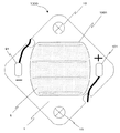
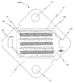
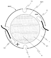
図1に本発明の発光装置1000を上面から見た模式図を示す。発光装置は、酸化アルミニウム(以下、アルミナとよぶ)基板1、発光部1001、正電極外部接続ランド101、負電極外部接続ランド91、取り付け部13のネジ、外部接続ランドに接続された外部配線、外部配線が通る外部配線用穴、第一の蛍光体含有封止樹脂層5から構成されている。
(Embodiment 1)
FIG. 1 shows a schematic view of a
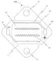
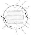
図2に本実施形態の発光装置の反射層および配線パターン等を示す。アルミナ基板1、アルミナ基板上の配線パターン2、チップ載置部41、正電極外部接続ランド101、負電極外部接続ランド91、取り付け部13、ボンディングワイヤ位置決めあるいはチップ搭載位置目安パターン42、アルミナ基板裏面に形成された反射層44から構成されている。
FIG. 2 shows a reflective layer, a wiring pattern, and the like of the light emitting device of this embodiment.
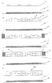
次に、図3(a)から(e)を参照して、発光装置1000の製造方法を以下に示す。
(a)アルミナ基板1厚さ1mmの片面に反射層44としてAg−Nd合金厚さ0.1mmをスパッタリング法を用いて形成する。その後、フォトエッチング法にてほぼ長方形状パターンを形成する。反射層44として、0.1mm程度の厚さがあれば、反射層としての効果がより得られる。また、Ag−Nd等の合金を用いる事により、Agの凝集を抑制し、反射率の低下を防ぐことができる。
Next, with reference to FIGS. 3A to 3E, a method for manufacturing the
(A)
また、アルミナ基板1厚さ1mm上面に金膜厚さ0.07mmをスパッタリング法を用いて形成する。その後、フォトエッチング法にて配線パターン形状2(幅1mm、間隔2mm)を形成する。ここで、配線パターン形状2は、ほぼ反射層44の形状と一致するような位置に形成されているが、反射層44は少なくとも配線パターン形状2の最外周部形状から外に出るように形成されている事が好ましい。そのように形成する事により、配線パターン間に設けられる各LEDチップからの光が、反射層の効果を一様に得る事ができ、色ずれが生じる事を避けるが可能となる。
(b)アルミナ基板上にLEDチップ3(短辺幅0.24mm、長辺0.48mm、厚み0.14mm)をエポキシ樹脂を用いて固定する。LEDチップ3と配線パターン2をボンディングワイヤWを用いて電気的接続する。
(c)アルミナ基板1上にほぼ長方形状のシリコーンゴムシート4を密着させる。
(d)次に、このシリコーンゴムシート4内に蛍光体を含む封止樹脂を注入し、この蛍光体を含む封止樹脂を熱硬化させ、第一の蛍光体含有封止樹脂層5を形成する。
Also, a gold film thickness of 0.07 mm is formed on the upper surface of the
(B) The LED chip 3 (short side width 0.24 mm, long side 0.48 mm, thickness 0.14 mm) is fixed on an alumina substrate using an epoxy resin. The
(C) A substantially rectangular
(D) Next, a sealing resin containing a phosphor is injected into the
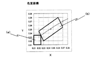
より具体的には、CIEの色度表で(x,y)=(0.345,0.35)となる光が得られるように下記蛍光物質と透光性樹脂であるシリコーン樹脂とが重量比が5:100となるように混合されたものを前記シリコーンゴムシート4内に注入した後、150℃の温度で60分硬化させ、第一の蛍光体含有封止樹脂層5を形成する。なお、色度範囲が図4の(b)領域内、たとえば黄色光を発光するように設定されている。また、上記色度範囲は本実施形態における好ましい範囲の一例であって、これに制限されるものではなく、取り出す光の光度に応じて適宜変更される。また、以下の実施形態においても同様である。
(e)その後にシリコーンゴムシート4を取り除き、発光部1001が形成される。
More specifically, the following fluorescent substance and the silicone resin, which is a translucent resin, are weighted so that light with (x, y) = (0.345, 0.35) is obtained in the CIE chromaticity table. The mixture mixed so as to have a ratio of 5: 100 is poured into the
(E) Thereafter, the
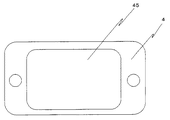
図19にシリコーンゴムシート4の概略図を示す。蛍光体を含有した透光性樹脂を注入する領域45から成っている。このため、シリコーンゴムシート4は蛍光体を含有した透光性樹脂を塗布する際のダム(樹脂漏れを防ぐ)のような機能を有している。したがって、前記シリコーンゴムシート4はダムシートと呼べるような特徴を有している。また、前記ダムシートは、何度も使用することが可能である。また、前記ダムシートの形状を変えることにより発光部の形状(蛍光体層の形状)を容易にいろいろと変えられることを特徴としている。
FIG. 19 shows a schematic view of the
次に、蛍光体を用いた発光装置に適用した本発明の効果について説明する。
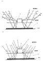
図23(a)(b)は、実施形態1の断面図を一部強調した模式図である。図23(a)に示した通り、本実施形態では、LEDチップからの光は、直接または反射層で反射して蛍光体に衝突し、蛍光体を励起して黄色光の発光がなされる。つまり、この反射層によって、基板に漏れる光が、反射層で反射されて、蛍光体含有封止樹脂層を通過するため、蛍光体により効率よく、たとえば黄色の光に変換されるので、演色性の高い発光装置となる。
Next, the effect of the present invention applied to a light emitting device using a phosphor will be described.
23A and 23B are schematic views partially highlighting the cross-sectional view of the first embodiment. As shown in FIG. 23A, in this embodiment, the light from the LED chip is reflected directly or by the reflection layer and collides with the phosphor, and the phosphor is excited to emit yellow light. In other words, the light that leaks to the substrate is reflected by the reflective layer and passes through the phosphor-containing sealing resin layer by this reflective layer, so that the phosphor is efficiently converted into, for example, yellow light. It becomes a high light emitting device.
また、蛍光体は封止樹脂内で沈降する場合(図23(b))があるが、本発明は基板側から光を反射するので、その場合であっても、反射層がなければ励起できない蛍光体までも励起する事が可能である。 Moreover, although a fluorescent substance may settle in sealing resin (FIG.23 (b)), since this invention reflects light from the board | substrate side, even in that case, it cannot excite without a reflective layer. Even phosphors can be excited.
よって、本実施の形態のように蛍光体を用いた発光装置においては、光を有効に活用し蛍光体を励起するので、たとえば黄色光の強い電球色が望まれる照明装置用の発光装置として特に好適である。なお、図23は、反射層を基板裏面に設けた実施形態であるが、基板内部に反射層を備える後述の実施形態においても同様の効果がある。 Therefore, in the light emitting device using the phosphor as in the present embodiment, the phosphor is excited by effectively utilizing the light, and therefore, particularly as a light emitting device for a lighting device in which a strong light bulb color with yellow light is desired. Is preferred. FIG. 23 shows an embodiment in which the reflective layer is provided on the back surface of the substrate. However, the same effect can be obtained in the later-described embodiment in which the reflective layer is provided inside the substrate.
また、基板をエッチングしてその窪みに反射層を設けている場合には、反射層は窪み内に納まり、発光装置を取り付ける際の機械的なダメージ(擦り傷・磨耗)などを避ける事が可能である。 In addition, when the substrate is etched and a reflective layer is provided in the dent, the reflective layer is stored in the dent and it is possible to avoid mechanical damage (abrasion / abrasion) etc. when mounting the light emitting device. is there.
また、配線パターン形状2を平行にし、配線パターン間にLEDチップ積載領域を設ける事により、LEDチップの載置ピッチを配線パターンと並行方向に自在に決めることが可能となり、発光装置の輝度調整、色度調整、放熱対策が容易にできる。
Also, by arranging the
本実施形態では、発光装置1000の外形形状をほぼ正方形状にし、発光部1001の形状はほぼ長方形状としたが、円形、楕円形等であってもよい。
In this embodiment, the outer shape of the
また、蛍光体層を形成する具体的材料としては、エポキシ樹脂、ユリア樹脂、シリコーン樹脂などの耐候性に優れた透明樹脂や、耐光性に優れたシリカゾル、硝子などの透光性無機材料が好適に用いられる。また、蛍光体と共に拡散剤を含有させても良い。具体的な拡散剤としては、チタン酸バリウム、酸化チタン、酸化アルミニウム、酸化珪素、炭酸カルシウム、二酸化珪素等が好適に用いられる。 In addition, as a specific material for forming the phosphor layer, transparent resins having excellent weather resistance such as epoxy resin, urea resin, silicone resin, and light-transmitting inorganic materials such as silica sol and glass having excellent light resistance are suitable. Used for. Moreover, you may contain a diffusing agent with fluorescent substance. As specific diffusing agents, barium titanate, titanium oxide, aluminum oxide, silicon oxide, calcium carbonate, silicon dioxide and the like are preferably used.
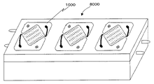
発光装置1000を用いて作製した照明器具の応用例として、図16に蛍光灯形LEDランプ8000、図18に電球形LEDランプ8002の模式図を示す。
As an application example of a lighting fixture manufactured using the light-emitting
以上、LEDチップとしては、サファイア基板上に窒化ガリウム系の発光部を形成した青色LEDチップを用いている。しかし、窒化ガリウム系化合物半導体よりなる青色系LEDチップに限らず、GaN基板上に青色系のLEDチップ、ZnO(酸化亜鉛)系化合物半導体よりなる青色系のLEDチップを使用してもよい。また、InGaAlP系、AlGaAs系化合物半導体のLEDチップを用いてもよいことは言うまでもない。 As described above, a blue LED chip in which a gallium nitride-based light emitting portion is formed on a sapphire substrate is used as the LED chip. However, it is not limited to a blue LED chip made of a gallium nitride compound semiconductor, and a blue LED chip made of a ZnO (zinc oxide) compound semiconductor may be used on a GaN substrate. It goes without saying that InGaAlP-based and AlGaAs-based compound semiconductor LED chips may be used.
蛍光体としては、Ce:YAG(セリウム賦活イットリウム・アルミニウム・ガーネット)蛍光体、Eu:BOSEあるいはSOSE(ユーロピウム賦活ストロンチウム・ガーネット)蛍光体、ユーロピウム賦活αサイアロン蛍光体等を好適に用いることができる。 As the phosphor, Ce: YAG (cerium activated yttrium aluminum garnet) phosphor, Eu: BOSE or SOSE (europium activated strontium garnet) phosphor, europium activated α sialon phosphor, and the like can be suitably used.
なお、樹脂封止体を形成する際にモールド用の封止樹脂を滴下していてもよい。また、金型を用いて樹脂封止体を形成してもよく、この樹脂封止体の形状として、樹脂封止体をたとえば上方に凸となる半球状の形状に形成して樹脂封止体にレンズとしての機能を持たせることも可能になる。 In addition, when forming the resin sealing body, the sealing resin for molds may be dripped. Further, the resin sealing body may be formed by using a mold. As the shape of the resin sealing body, for example, the resin sealing body is formed in a hemispherical shape that protrudes upward. It is also possible to have a lens function.
また、LEDチップの接着は熱硬化性樹脂などによって行なうことができる。具体的には、エポキシ樹脂、アクリル樹脂やイミド樹脂などが挙げられる。 The LED chip can be bonded with a thermosetting resin or the like. Specifically, an epoxy resin, an acrylic resin, an imide resin, etc. are mentioned.
なお、LEDチップの一方の面にP側電極およびN側電極が形成され、その面を上面として2本のワイヤボンディングを行なった状態を示した。また、LEDチップとして青色発光を示したが、発光色はこれに限定されず、たとえば紫外線発光のものや緑色発光のものを用いてもよい。また、LEDチップから発する光を蛍光体によって変換して白色を得る方法を示したが、蛍光体を用いずにたとえば赤、緑、青の3色のLEDチップをそれぞれ用いて白色、電球色など照明に必要な色を得ても良い。 In addition, the P side electrode and the N side electrode were formed on one surface of the LED chip, and the state where two wires were bonded with the surfaces as the upper surface was shown. Moreover, although blue light emission was shown as an LED chip, the luminescent color is not limited to this, For example, the thing of ultraviolet light emission and the thing of green light emission may be used. Moreover, although the method of obtaining the white color by converting the light emitted from the LED chip with the phosphor has been shown, white, light bulb color, etc. using, for example, red, green, and blue LED chips without using the phosphor. You may get the color you need for lighting.
また基板はアルミナ以外にセラミック基板でもよい。いずれの基板も熱膨張が小さく、熱伝導が良く、より高い放熱性と耐熱性を要求される用途に対してはより熱伝導性に優れているために、駆動電流として大電流が供給できる。さらにまた、LEDチップの信頼性の向上ができ、LEDチップからの熱による蛍光体の劣化を抑えることができる。 The substrate may be a ceramic substrate other than alumina. Since any of the substrates has a small thermal expansion, good thermal conductivity, and higher thermal conductivity for applications requiring higher heat dissipation and heat resistance, a large current can be supplied as a drive current. Furthermore, the reliability of the LED chip can be improved, and deterioration of the phosphor due to heat from the LED chip can be suppressed.
特に、セラミック基板は高い絶縁性を有しているために、基板上に絶縁層を形成しなくてもよいため、作製が容易となる。また、配線パターン側面とLEDチップ側面の間隔が沿面距離の確保が不要となる。 In particular, since the ceramic substrate has high insulating properties, it is not necessary to form an insulating layer on the substrate, so that the production becomes easy. Further, it is not necessary to secure a creepage distance between the side surface of the wiring pattern and the side surface of the LED chip.
さらに、セラミック基板の上に配線パターンを直接形成でき、ソルダーレジストを必要としない。配線を半田等で熱接続する際に生じていたソルダーレジストの変色問題もなくなる。さらに、発光素子の発熱によるソルダーレジストの変色問題もなくなる。 Furthermore, a wiring pattern can be directly formed on the ceramic substrate, and no solder resist is required. The problem of discoloration of the solder resist that has occurred when the wiring is thermally connected with solder or the like is also eliminated. Further, the problem of discoloration of the solder resist due to heat generation of the light emitting element is eliminated.
いずれにしても上記LEDチップ搭載に好適な基板は搭載したLEDチップから基板への光の漏れが生じる。 In any case, the substrate suitable for mounting the LED chip causes light leakage from the mounted LED chip to the substrate.
以下、実施形態1の発光装置の一部を変更した他の実施形態について説明する。実施形態1との共通の部分に関しては説明を省略して、それぞれの実施形態の特徴部分について記載する。
Hereinafter, another embodiment in which a part of the light-emitting device of
(実施形態2)
実施形態2の発光装置を、図5に示す。本実施の形態は基板の内部に反射層を設けたものである。
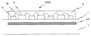
(Embodiment 2)
The light emitting device of
図5は、発光部1002の断面から見た模式図である。セラミック基板1内に、反射層44としてMo(モリブデン)厚さ0.1mmが形成されている。具体的には、たとえば2枚のセラミック板の間に反射層44を挟む。反射層44は、たとえば実施形態1と同様にスパッタリング法およびフォトエッチング法を用いて形成される。
FIG. 5 is a schematic view seen from the cross section of the
この基板内部へ反射層を設ける構成により、反射層を基板に漏れた光を有効に反射しえる位置に形成でき、かつ、基板全体の厚みを厚くして機械的強度や放熱効果をさらに高める利点がある。また、Moは、熱膨張係数が基板とほぼ同じであるため、基板と反射層の熱膨張係数の差から生じる破損を防止することができ、発光装置の信頼性を確保する事が可能となる。 With the configuration in which the reflective layer is provided inside the substrate, the reflective layer can be formed at a position where the light leaking to the substrate can be effectively reflected, and the overall thickness of the substrate is increased to further increase the mechanical strength and the heat dissipation effect. There is. Moreover, since Mo has a thermal expansion coefficient substantially the same as that of the substrate, it is possible to prevent damage resulting from the difference in the thermal expansion coefficient between the substrate and the reflective layer, and to ensure the reliability of the light emitting device. .
次に、配線パターン2を形成する。上記実施形態1でも説明したように、反射層44が少なくとも配線パターン形状2の最外周部形状から外に出るように形成されている事が好ましい。次に、LEDチップをセラミック基板にエポキシ樹脂を用いて接合し、さらに、LEDチップ3と配線パターン2をボンディングワイヤWを用いて電気的接続する。LEDチップ3、配線パターン2とボンディングワイヤWを覆うように蛍光体の含有された封止樹脂5を形成する。
Next, the
よって、発光部1002が作製される。
本実施形態の発光装置は、実施形態1と同様に、基板側から漏れる光を有効に活用する事ができる。また、反射層がセラミック基板内部にあるので、基板強度があり、さらに、発光装置を取り付ける際の機械的なダメージ(擦り傷・磨耗)などを避ける事が可能である。
Therefore, the
As in the first embodiment, the light emitting device according to the present embodiment can effectively utilize light leaking from the substrate side. In addition, since the reflective layer is inside the ceramic substrate, the substrate has strength, and further, mechanical damage (abrasion / abrasion) when the light-emitting device is attached can be avoided.
(実施形態3)
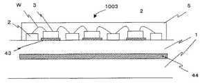
実施形態3の発光装置を、図6に示す。
(Embodiment 3)
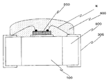
The light emitting device of
図6は、発光部1003の断面から見た模式図である。セラミック基板1内に、第二反射層44として銀層厚さ0.02mmが形成されている。次に、配線パターン2とLEDチップ搭載部および第一反射層43としての銀層厚さ0.05mmを形成する。
FIG. 6 is a schematic view seen from the cross section of the
ここで、反射層44が少なくとも配線パターン形状2の最外周部形状から外に出るように形成する。次に、LEDチップ3をシリコーン樹脂を用いてLEDチップ搭載部および第一反射層43に接合する。次に、LEDチップ3と配線パターン2をボンディングワイヤWを用いて電気的接続する。LEDチップ3、配線パターン2とボンディングワイヤWを覆うように蛍光体の含有された封止樹脂5を形成する。
Here, the
よって、発光部1003が作製される。
本実施形態の発光装置は、複数の反射層を有しており、実施形態1および2よりも、より高精度に基板側から光が漏れる光を有効に活用する事ができる。また、第一反射層に共晶チップが使用でき、蛍光体が黄色発光の場合は、より黄色光が強い電球色を持つ発光装置が作製できる。
Therefore, the
The light-emitting device of this embodiment has a plurality of reflective layers, and can effectively use light leaking from the substrate side with higher accuracy than in the first and second embodiments. Further, when a eutectic chip can be used for the first reflective layer and the phosphor emits yellow light, a light emitting device having a light bulb color with stronger yellow light can be produced.
(実施形態4)
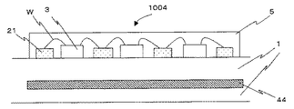
次に、実施形態4の発光装置を、図7に示す。
(Embodiment 4)
Next, the light-emitting device of
図7は、発光部1004の断面から見た模式図である。セラミック基板1内に、反射層44として銀膜厚さ0.1mmが形成されている。次に、セラミック基板1上に配線パターン21を形成する。ここで、配線パターン21は反射層44の形状内に入るように形成する。
FIG. 7 is a schematic view seen from the cross section of the
次に、LEDチップ3をエポキシ樹脂を用いてセラミック基板1に接合する。次に、LEDチップ3と配線パターン2をボンディングワイヤWを用いて電気的接続する。LEDチップ3、配線パターン21をボンディングワイヤWを覆うように蛍光体の含有された封止樹脂5を形成する。ここで、配線パターン21として透明導電体膜を用いた。透明導電体膜を用いる事により、配線パターン21での光損失を抑え、取り出す光量が増加させる事ができる。本実施形態では、透明導電体膜として、具体的にはITOを用いているが、他にはIn2O3(酸化インジウム)、SnO2(酸化スズ)、ZnO(酸化亜鉛)、Sn(スズ)ドープIn2O3,Sb(アンチモン)ドープSnO2等も適用できる。なお、配線パターンの厚さは0.010mm、幅は0.7mmとした。
Next, the
(実施形態5)
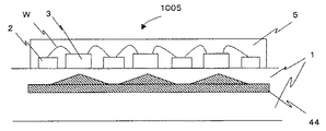
次に、実施形態5の発光装置を、図8に示す。
(Embodiment 5)
Next, a light-emitting device of
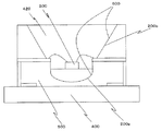
図8は、発光部1005の断面から見た模式図である。セラミック基板1内に、反射層44としてMo(モリブデン)厚さ0.07mmが形成されている。
FIG. 8 is a schematic view seen from the cross section of the
本実施形態における反射層44は、凹凸状に形成され、凸部はLEDチップのほぼ下方に位置するようにLEDチップを搭載する。このような凹凸形状の反射層44を用いる事により、セラミック基板1に照射される光をLEDチップのほぼ下方の反射層の凸部で角度をつけて拡散し、LEDチップ下面に光が戻るのを防ぐことができる。よって、LEDチップ下面での光損失を抑制する事が可能となる。また、反射層44の凹凸のパターンとしては、凸部がLEDチップ下方にあればよく、ストライプ状であってもよいし、ドット状であってもよい。また、凸部がLEDチップの下方にない場合であっても、光拡散の効果が得られる。
The
次に、セラミック基板1上に配線パターン2を形成する。ここで、配線パターン2は反射層44の形状内に入るように形成する。次に、LEDチップ3をエポキシ樹脂を用いてセラミック基板1に接合する。次に、LEDチップ3と配線パターン2をボンディングワイヤWを用いて電気的接続する。LEDチップ3、配線パターン2とボンディングワイヤWを覆うように蛍光体の含有された封止樹脂5を形成する。
Next, the
(実施形態6)
次に、実施形態6の発光装置を説明する。
(Embodiment 6)
Next, the light emitting device of Embodiment 6 will be described.
本実施形態は、蛍光体含有封止樹脂層を2層にすることにより、外部へ照射される光の色度をより正確に制御する事を可能とするものである。 This embodiment makes it possible to more accurately control the chromaticity of light irradiated to the outside by using two phosphor-containing sealing resin layers.
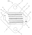
図9に本発明の発光装置2000を上面から見た模式図を示す。発光装置は、酸化アルミニウム(以下、アルミナとよぶ)基板1、発光部2001、正電極外部接続ランド101、負電極外部接続ランド91、取り付け部13のネジ、外部接続ランドに接続された外部配線、外部配線が通る外部配線用穴、第一の蛍光体含有封止樹脂層5、第一の蛍光体含有封止樹脂層5上に塗布された第二の蛍光体含有封止樹脂層51から構成されている。
FIG. 9 shows a schematic view of the
図10に本実施形態の発光装置の配線パターンと上面反射層等を示す。アルミナ基板1、アルミナ基板上の配線パターン2、第一反射層43およびチップ載置部41、正電極外部接続ランド101、負電極外部接続ランド91、取り付け部13、ボンディングワイヤ位置決めあるいはチップ搭載位置目安パターン42、第二反射層44から構成されている。
FIG. 10 shows a wiring pattern, a top reflective layer, and the like of the light emitting device of this embodiment.
図22(a)から(e)に発光装置2000の製造方法を以下に示す。
(a)アルミナ基板1厚さ1mm内に第二反射層44として、Ag厚さ0.1mmが形成されたアルミナ基板1を準備する。ここで、第二反射層44はほぼ長方形状パターンとする。
22A to 22E show a method for manufacturing the
(A)
アルミナ基板1表面上に配線パターンとして金膜厚さ0.07mmをスパッタリング法を用いて形成する。その後、フォトエッチング法にて配線パターン形状2(幅1mm、間隔2mm)を形成する。ここで、配線パターン形状2は、ほぼ第二反射層44の形状と一致するような位置に形成する。次に、アルミナ基板1表面上に第一反射層43およびチップ載置部41として、銀メッキ法にて銀箔膜0.01mm、長さ9mm、幅0.5mmを形成する。
(b)前記第一反射層43およびチップ載置部41上にLEDチップ3(短辺幅0.24mm、長辺0.48mm、厚み0.14mm)をエポキシ樹脂を用いて固定する。LEDチップ3と配線パターン2をボンディングワイヤWを用いて電気的接続する。
(c)アルミナ基板1上にほぼ長方形状のシリコーンゴムシート4を密着させる。
(d)次に、このシリコーンゴムシート4内に第一の蛍光体を含む封止樹脂5を注入し、この蛍光体を含む封止樹脂を熱硬化させる。
A gold film thickness of 0.07 mm is formed as a wiring pattern on the surface of the
(B) The LED chip 3 (short side width 0.24 mm, long side 0.48 mm, thickness 0.14 mm) is fixed on the first
(C) A substantially rectangular
(D) Next, the sealing
より具体的には、CIEの色度表で(x,y)=(0.325,0.335)となる光が得られるように、下記蛍光物質と透光性樹脂であるシリコーン樹脂とが重量比が5:100となるように混合されたものを前記シリコーンゴムシート4内に注入した後、150℃の温度で30分硬化させ蛍光体を含む封止樹脂体5を形成する。色度範囲が図4の(a)領域内に入るように形成する。
More specifically, the following fluorescent substance and a silicone resin which is a translucent resin are used so that light with (x, y) = (0.325, 0.335) is obtained in the CIE chromaticity table. After the mixture having been mixed so that the weight ratio is 5: 100 is poured into the
次に、発光装置2000の色度特性を測定する。色度範囲が図4の(b)領域内に入っていない場合、第一の蛍光体を含有した透光性樹脂5上にCIEの色度表でx、y=(0.345、0.35)となる光が得られるように下記蛍光物質と透光性樹脂であるシリコーン樹脂とが重量比が2:100となるように混合されたものを前記シリコーンゴムシート内に注入した後、150℃の温度で1時間硬化させ蛍光体を含む封止樹脂体51を形成する。
Next, the chromaticity characteristics of the
再度、発光装置2000の色度特性を測定する。色度範囲が図4の(b)領域内に入っていると、発光部2001が製造される。
(e)その後にシリコーンゴムシート4を取り除き、発光部2001が形成される。
Again, the chromaticity characteristics of the
(E) Thereafter, the
本実施形態では、第一の蛍光体含有封止樹脂層5および第二の蛍光体含有封止樹脂層51の2層の蛍光体封止樹脂層を有し、上述したようにそれぞれにおいて、所定の色度範囲に入るように制御して発光装置を形成している。したがって、より正確に外部へ照射される光の色度を制御する事が可能となる。
In the present embodiment, there are two phosphor encapsulating resin layers, a first phosphor-containing
また、第1反射層として共晶チップが使用でき、より黄色光の強い電球色を持つ発光装置を作製する事も可能である。 Further, a eutectic chip can be used as the first reflective layer, and a light emitting device having a light bulb color with a stronger yellow light can be produced.
なお、発光装置2000の外形形状をほぼ正方形状にし、発光部2001の形状はほぼ長方形状としたが、円形、楕円形等であっても本発明は適用が可能である。
Note that although the outer shape of the
次に、実施形態6の別形態を図11に示す。
図11は、発光装置の配線パターンと上面の反射層等を示している。アルミナ基板1、アルミナ基板上の配線パターン2、第一反射層43およびチップ載置部41、正電極外部接続ランド101、負電極外部接続ランド91、取り付け部13、ボンディングワイヤ位置決めあるいはチップ搭載位置目安パターン42、第二反射層44から構成されている。
Next, another embodiment of the sixth embodiment is shown in FIG.
FIG. 11 shows a wiring pattern of the light emitting device, a reflective layer on the upper surface, and the like.
第一反射層43およびチップ載置部41の形状が違うのみで、発光装置の作製方法(LEDチップの搭載、蛍光体含有封止樹脂の形成方法など)は、実施形態6と同様である。第一反射層43およびチップ載置部41の形状は、ほぼ丸形で、直径0.6mm、ピッチ0.738mm、配線パターンに対しての間隔は、ほぼ真ん中1mmの位置とした。
Only the shapes of the first
ここで作製された発光装置を3000とする。ここで、第二反射層44は、アルミナ基板1内に形成されている。
The light emitting device manufactured here is assumed to be 3000. Here, the second
次に、実施形態6の別形態を図12に示す。
図12は、別形態の発光装置4000を上面から見た模式図である。発光装置は、アルミナ基板1、発光部4001、正電極外部接続ランド101、負電極外部接続ランド91、取り付け部13、第一蛍光体含有封止樹脂層5で構成されている。
Next, another embodiment of the sixth embodiment is shown in FIG.
FIG. 12 is a schematic view of another embodiment of the
ここで、発光装置4000の外形形状をほぼ正方形状にした。発光部4001の形状はほぼ円形状とした。
Here, the outer shape of the light-emitting
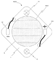
図13は、別形態の発光装置5000を上面から見た模式図を示す。発光装置は、アルミナ基板1、発光部5001、正電極外部接続ランド101、負電極外部接続ランド91、取り付け部13、第一蛍光体含有封止樹脂層5、第一蛍光体含有封止樹脂層5上のほぼ全面に塗布された第二蛍光体含有封止樹脂層51から構成されている。ここで、発光装置5000の外形状は円形で、発光部5001は六角形状をしている。
FIG. 13 is a schematic view of another embodiment of the
ここで、第一反射層43およびチップ載置部41がセラミック基板1上に形成されている。直径は0.5mm、ピッチ0.75mmとした。また、第二反射層44は発光部5001とほぼ同じ六角形状とした。
Here, the first
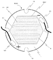
図14は、別形態の発光装置6000を上面から見た模式図を示す。発光装置は、セラミック基板1、発光部6001、正電極外部接続ランド101、負電極外部接続ランド91、取り付け部13、第一蛍光体含有封止樹脂層5から構成されている。ここで、発光装置6000の外形状は円形で、発光部6001も円形状をしている。また、反射層44は発光部6001とほぼ同じ円形状とした。
FIG. 14 is a schematic view of another embodiment of the
図15は、別形態の発光装置7000を上面から見た模式図を示す。発光装置は、セラミック基板1、発光部7001、正電極外部接続ランド101、負電極外部接続ランド91、取り付け部13、長方形状に形成された第一蛍光体含有封止樹脂層5、前記第一蛍光体含有封止樹脂層5上に部分的に塗布された第二蛍光体含有封止樹脂層51から構成されている。ここで、発光装置7000の外形状は円形で、発光部7001は長方形状をしている。また、反射層44は発光部7001とほぼ同じ長方形状とした。
FIG. 15 is a schematic view of another embodiment of the
以上、別形態を含めた実施形態1から6に記載の各実施形態の発光装置は、発光装置および発光部の外形状を適宜変更する事により、図16または図17の発光装置として適用して応用例である照明器具は作製できる。また、図18に示した応用例である照明器具も作製可能である。
As described above, the light emitting device of each embodiment described in
また、実施形態で示した発光装置は、いずれもLEDチップからの光を、発光素子が設けられた基板裏面(発光素子が設けられた面と反対の面)もしくは基板内部に反射層を設けることにより、基板側に漏れてくる光を反射させて外部に取り出す光量を増やす事が可能である。特に、照明器具に用いる発光装置においては、光の出力が大きいLEDを用いるため、基板に漏れる光の損失が問題であり、本願発明が好適に適用できる。 In any of the light-emitting devices shown in the embodiments, the light from the LED chip is provided with a reflective layer on the back surface of the substrate on which the light-emitting elements are provided (the surface opposite to the surface on which the light-emitting elements are provided) or inside the substrate Thus, it is possible to increase the amount of light extracted by reflecting light leaking to the substrate side. In particular, in a light-emitting device used for a lighting fixture, an LED having a large light output is used, and thus a loss of light leaking to the substrate is a problem, and the present invention can be suitably applied.
また、本願発明の発光装置は、上記実施形態の説明でも述べたように、色ずれが少ないという効果があり、照明装置と同様に、均一的な光照射が求められる表示装置等のバックライト照明用としても、有効に適用が可能である。 In addition, as described in the above embodiment, the light-emitting device of the present invention has an effect that there is little color misregistration and, like the illumination device, backlight illumination such as a display device that requires uniform light irradiation. It can be effectively applied even for use.
さらに、本願発明では、発光素子としてLEDチップを用いているが、これに限定される事なく他の発光素子を採用した場合でも適用は可能であり、複数のLEDチップを用いた発光装置に限らず、一つのLEDチップを搭載した発光装置においても、上述の効果は得られ適用できる。 Furthermore, in this invention, although the LED chip is used as a light emitting element, even if it employs other light emitting elements without being limited to this, it can be applied, and is limited to a light emitting device using a plurality of LED chips. In addition, the above-described effects can be obtained and applied to a light-emitting device equipped with one LED chip.
また、今回開示された上記各実施の形態はすべての点で例示であって、制限的なものではないと考えられるべきである。本発明の技術的範囲は特許請求の範囲によって画定され、また特許請求の範囲の記載と均等の意味および範囲内でのすべての変更が含まれることが意図される。 In addition, it should be considered that the above-described embodiments disclosed herein are illustrative in all respects and are not restrictive. The technical scope of the present invention is defined by the terms of the claims, and is intended to include any modifications within the scope and meaning equivalent to the terms of the claims.
1 基板、2 配線パターン、3 LEDチップ、4 シリコーンゴムシート、W ボンディングワイヤ、5 第一の蛍光体を含有した透光性樹脂、51 第二の蛍光体を含有した透光性樹脂、101 正電極配線パターン、91 負電極配線パターン、41 チップ搭載部、43 第一反射層、44 反射層あるいは第二反射層、1000,2000,3000,4000,5000,6000,7000 発光装置、1001,1002,1003,1004,1005,4001,5001,6001,7001 発光部、8000,8001 蛍光灯形LEDランプ、8002 電球形LEDランプ。
DESCRIPTION OF
Claims (16)
前記基板に設けられた発光素子と、前記発光素子を覆い前記発光素子によって励起される蛍光体を含む封止樹脂と、
前記基板の前記発光素子の設けられた面と反対の面に設けられた第1反射層とを有することを特徴とする発光装置。 A substrate,
A light-emitting element provided on the substrate; a sealing resin that covers the light-emitting element and includes a phosphor excited by the light-emitting element;
A light emitting device comprising: a first reflective layer provided on a surface of the substrate opposite to the surface on which the light emitting element is provided.
前記基板に設けられた発光素子と、前記発光素子を覆い前記発光素子によって励起される蛍光体を含む封止樹脂と、
前記基板の内部に設けられた第1反射層とを有することを特徴とする発光装置。 A substrate,
A light-emitting element provided on the substrate; a sealing resin that covers the light-emitting element and includes a phosphor excited by the light-emitting element;
A light emitting device comprising: a first reflective layer provided inside the substrate.
前記第1反射層は、前記少なくとも2枚の基板に挟まれていることを特徴とする請求項3に記載の発光装置。 The substrate is configured by bonding at least two substrates,
The light emitting device according to claim 3, wherein the first reflective layer is sandwiched between the at least two substrates.
Priority Applications (1)
| Application Number | Priority Date | Filing Date | Title |
|---|---|---|---|
| JP2007088427A JP5084324B2 (en) | 2007-03-29 | 2007-03-29 | Light emitting device and lighting device |
Applications Claiming Priority (1)
| Application Number | Priority Date | Filing Date | Title |
|---|---|---|---|
| JP2007088427A JP5084324B2 (en) | 2007-03-29 | 2007-03-29 | Light emitting device and lighting device |
Publications (2)
| Publication Number | Publication Date |
|---|---|
| JP2008251663A true JP2008251663A (en) | 2008-10-16 |
| JP5084324B2 JP5084324B2 (en) | 2012-11-28 |
Family
ID=39976302
Family Applications (1)
| Application Number | Title | Priority Date | Filing Date |
|---|---|---|---|
| JP2007088427A Expired - Fee Related JP5084324B2 (en) | 2007-03-29 | 2007-03-29 | Light emitting device and lighting device |
Country Status (1)
| Country | Link |
|---|---|
| JP (1) | JP5084324B2 (en) |
Cited By (15)
| Publication number | Priority date | Publication date | Assignee | Title |
|---|---|---|---|---|
| WO2011004798A1 (en) * | 2009-07-06 | 2011-01-13 | 株式会社 東芝 | Element mounting ceramic substrate, led mounting ceramic substrate, led lamp, and head light, and electronic component |
| WO2011070697A1 (en) * | 2009-12-07 | 2011-06-16 | パナソニック株式会社 | Light-emitting module and method for manufacturing same |
| JP2011151187A (en) * | 2010-01-21 | 2011-08-04 | Citizen Electronics Co Ltd | Semiconductor light-emitting device and method of manufacturing semiconductor light-emitting device |
| JP2011258611A (en) * | 2010-06-04 | 2011-12-22 | Sharp Corp | Light-emitting device |
| JP2012222011A (en) * | 2011-04-05 | 2012-11-12 | Panasonic Corp | Led light-emitting module and luminaire using the same |
| JP5073872B2 (en) * | 2011-01-18 | 2012-11-14 | パナソニック株式会社 | Light bulb shaped lamp and lighting device |
| JP2012529150A (en) * | 2009-06-02 | 2012-11-15 | ブリッジラックス インコーポレイテッド | Light source having optical components for generating a spherical emission pattern |
| JP2012227290A (en) * | 2011-04-18 | 2012-11-15 | Panasonic Corp | Light emitting device, back light unit, liquid crystal display device, and lighting device |
| JP2014187392A (en) * | 2014-06-23 | 2014-10-02 | Sharp Corp | Light-emitting device and luminaire having the same |
| US9018832B2 (en) | 2010-09-30 | 2015-04-28 | Sharp Kabushiki Kaisha | Light-emitting device and lighting device provided with the same |
| EP2858132A4 (en) * | 2012-05-31 | 2015-05-27 | Panasonic Ip Man Co Ltd | ELECTROLUMINESCENT DIODE MODULE |
| JP2016042602A (en) * | 2015-12-17 | 2016-03-31 | シャープ株式会社 | Light-emitting device and lighting apparatus |
| US9577153B2 (en) | 2012-02-20 | 2017-02-21 | Sharp Kabushiki Kaisha | Light emission device and illumination device |
| KR20170116211A (en) * | 2009-02-09 | 2017-10-18 | 에피스타 코포레이션 | Light emitting device |
| US10107477B2 (en) | 2010-11-11 | 2018-10-23 | Bridgelux Inc. | LED light using internal reflector |
Citations (6)
| Publication number | Priority date | Publication date | Assignee | Title |
|---|---|---|---|---|
| JPH0945965A (en) * | 1995-07-26 | 1997-02-14 | Nichia Chem Ind Ltd | Ceramic LED package and manufacturing method thereof |
| JP2001148509A (en) * | 1999-11-18 | 2001-05-29 | Matsushita Electric Works Ltd | Illumination light source |
| JP2005093896A (en) * | 2003-09-19 | 2005-04-07 | Stanley Electric Co Ltd | Semiconductor light emitting device |
| JP2005191192A (en) * | 2003-12-25 | 2005-07-14 | Kyocera Corp | Light emitting element mounting substrate and light emitting device |
| JP2005244152A (en) * | 2004-01-29 | 2005-09-08 | Kyocera Corp | Light emitting element mounting substrate and light emitting device |
| JP2006344925A (en) * | 2005-05-11 | 2006-12-21 | Sharp Corp | Light emitting element mounting frame and light emitting device |
-
2007
- 2007-03-29 JP JP2007088427A patent/JP5084324B2/en not_active Expired - Fee Related
Patent Citations (6)
| Publication number | Priority date | Publication date | Assignee | Title |
|---|---|---|---|---|
| JPH0945965A (en) * | 1995-07-26 | 1997-02-14 | Nichia Chem Ind Ltd | Ceramic LED package and manufacturing method thereof |
| JP2001148509A (en) * | 1999-11-18 | 2001-05-29 | Matsushita Electric Works Ltd | Illumination light source |
| JP2005093896A (en) * | 2003-09-19 | 2005-04-07 | Stanley Electric Co Ltd | Semiconductor light emitting device |
| JP2005191192A (en) * | 2003-12-25 | 2005-07-14 | Kyocera Corp | Light emitting element mounting substrate and light emitting device |
| JP2005244152A (en) * | 2004-01-29 | 2005-09-08 | Kyocera Corp | Light emitting element mounting substrate and light emitting device |
| JP2006344925A (en) * | 2005-05-11 | 2006-12-21 | Sharp Corp | Light emitting element mounting frame and light emitting device |
Cited By (27)
| Publication number | Priority date | Publication date | Assignee | Title |
|---|---|---|---|---|
| KR20170116211A (en) * | 2009-02-09 | 2017-10-18 | 에피스타 코포레이션 | Light emitting device |
| KR102116359B1 (en) * | 2009-02-09 | 2020-05-29 | 에피스타 코포레이션 | Light emitting device |
| JP2012529150A (en) * | 2009-06-02 | 2012-11-15 | ブリッジラックス インコーポレイテッド | Light source having optical components for generating a spherical emission pattern |
| US8922106B2 (en) | 2009-06-02 | 2014-12-30 | Bridgelux, Inc. | Light source with optics to produce a spherical emission pattern |
| WO2011004798A1 (en) * | 2009-07-06 | 2011-01-13 | 株式会社 東芝 | Element mounting ceramic substrate, led mounting ceramic substrate, led lamp, and head light, and electronic component |
| JP5839992B2 (en) * | 2009-07-06 | 2016-01-06 | 株式会社東芝 | LED lamp and headlight |
| EP2484957A4 (en) * | 2009-07-06 | 2015-09-30 | Toshiba Kk | CERAMIC ELEMENT MOUNTING SUBSTRATE, CERAMIC LIGHT EMITTING DIODE MOUNTING SUBSTRATE, LIGHT EMITTING DIODE LAMP, HEADLIGHT, AND ELECTRONIC COMPONENT |
| JP2015019106A (en) * | 2009-07-06 | 2015-01-29 | 株式会社東芝 | Ceramic substrate for mounting element, and electronic part |
| US9095051B2 (en) | 2009-07-06 | 2015-07-28 | Kabushiki Kaisha Toshiba | Ceramic substrate for mounting a device, ceramic substrate for mounting an LED, LED lamp, headlight and electronic parts |
| WO2011070697A1 (en) * | 2009-12-07 | 2011-06-16 | パナソニック株式会社 | Light-emitting module and method for manufacturing same |
| JP2011151187A (en) * | 2010-01-21 | 2011-08-04 | Citizen Electronics Co Ltd | Semiconductor light-emitting device and method of manufacturing semiconductor light-emitting device |
| JP2011258611A (en) * | 2010-06-04 | 2011-12-22 | Sharp Corp | Light-emitting device |
| US9188321B2 (en) | 2010-09-30 | 2015-11-17 | Sharp Kabushiki Kaisha | Light-emitting device and lighting device provided with the same |
| US9018832B2 (en) | 2010-09-30 | 2015-04-28 | Sharp Kabushiki Kaisha | Light-emitting device and lighting device provided with the same |
| US9735133B2 (en) | 2010-09-30 | 2017-08-15 | Sharp Kabushiki Kaisha | Light-emitting device and lighting device provided with the same |
| US9243791B2 (en) | 2010-09-30 | 2016-01-26 | Sharp Kabushiki Kaisha | Light-emitting device and lighting device provided with the same |
| US9490236B2 (en) | 2010-09-30 | 2016-11-08 | Sharp Kabushiki Kaisha | Light-emitting device and lighting device provided with the same |
| US10107477B2 (en) | 2010-11-11 | 2018-10-23 | Bridgelux Inc. | LED light using internal reflector |
| JP5073872B2 (en) * | 2011-01-18 | 2012-11-14 | パナソニック株式会社 | Light bulb shaped lamp and lighting device |
| JP2012222011A (en) * | 2011-04-05 | 2012-11-12 | Panasonic Corp | Led light-emitting module and luminaire using the same |
| JP2012227290A (en) * | 2011-04-18 | 2012-11-15 | Panasonic Corp | Light emitting device, back light unit, liquid crystal display device, and lighting device |
| US9577153B2 (en) | 2012-02-20 | 2017-02-21 | Sharp Kabushiki Kaisha | Light emission device and illumination device |
| EP2858132A4 (en) * | 2012-05-31 | 2015-05-27 | Panasonic Ip Man Co Ltd | ELECTROLUMINESCENT DIODE MODULE |
| CN104350618B (en) * | 2012-05-31 | 2017-07-25 | 松下知识产权经营株式会社 | Led module |
| US9437581B2 (en) | 2012-05-31 | 2016-09-06 | Panasonic Intellectual Property Management Co., Ltd. | LED module |
| JP2014187392A (en) * | 2014-06-23 | 2014-10-02 | Sharp Corp | Light-emitting device and luminaire having the same |
| JP2016042602A (en) * | 2015-12-17 | 2016-03-31 | シャープ株式会社 | Light-emitting device and lighting apparatus |
Also Published As
| Publication number | Publication date |
|---|---|
| JP5084324B2 (en) | 2012-11-28 |
Similar Documents
| Publication | Publication Date | Title |
|---|---|---|
| JP5084324B2 (en) | Light emitting device and lighting device | |
| US12080695B2 (en) | Method for manufacturing light emitting devices | |
| JP6868388B2 (en) | Light emitting device and integrated light emitting device | |
| JP5089212B2 (en) | LIGHT EMITTING DEVICE, LED LAMP USING THE SAME, AND METHOD FOR MANUFACTURING LIGHT EMITTING DEVICE | |
| JP5648422B2 (en) | Light emitting device and manufacturing method thereof | |
| JP5118110B2 (en) | Light emitting device | |
| JP2012099544A (en) | Manufacturing method of light-emitting apparatus | |
| JP2008235824A5 (en) | ||
| CN112838156A (en) | light-emitting device | |
| JP2008227412A (en) | Light emitting device and manufacturing method thereof | |
| JP6628739B2 (en) | Light emitting device | |
| JP5442534B2 (en) | Light emitting device | |
| JP5730711B2 (en) | Light emitting device | |
| KR20170043126A (en) | High power led package and method of the same improved color coordinates and thermal conductivity | |
| JP2005285871A (en) | LIGHT EMITTING DEVICE, ITS MANUFACTURING METHOD, AND LIGHTING DEVICE | |
| JP2015092622A (en) | Light emitting device | |
| JP6985622B2 (en) | Light emitting device and integrated light emitting device | |
| JP5752841B2 (en) | Light emitting device and manufacturing method thereof | |
| JP5829316B2 (en) | Light emitting device and manufacturing method thereof | |
| JP6242437B2 (en) | Light emitting device | |
| JP6030193B2 (en) | Light emitting device substrate | |
| JP2024113533A (en) | Light-emitting device | |
| JP5980860B2 (en) | LED lamp | |
| JP2023148970A (en) | Light emitting device and its manufacturing method | |
| JP5312556B2 (en) | Light emitting device and lighting device |
Legal Events
| Date | Code | Title | Description |
|---|---|---|---|
| A621 | Written request for application examination |
Free format text: JAPANESE INTERMEDIATE CODE: A621 Effective date: 20090218 |
|
| A977 | Report on retrieval |
Free format text: JAPANESE INTERMEDIATE CODE: A971007 Effective date: 20110823 |
|
| A131 | Notification of reasons for refusal |
Free format text: JAPANESE INTERMEDIATE CODE: A131 Effective date: 20110830 |
|
| A521 | Request for written amendment filed |
Free format text: JAPANESE INTERMEDIATE CODE: A523 Effective date: 20111024 |
|
| A131 | Notification of reasons for refusal |
Free format text: JAPANESE INTERMEDIATE CODE: A131 Effective date: 20111227 |
|
| A521 | Request for written amendment filed |
Free format text: JAPANESE INTERMEDIATE CODE: A523 Effective date: 20120220 |
|
| A02 | Decision of refusal |
Free format text: JAPANESE INTERMEDIATE CODE: A02 Effective date: 20120424 |
|
| A521 | Request for written amendment filed |
Free format text: JAPANESE INTERMEDIATE CODE: A523 Effective date: 20120629 |
|
| A911 | Transfer to examiner for re-examination before appeal (zenchi) |
Free format text: JAPANESE INTERMEDIATE CODE: A911 Effective date: 20120706 |
|
| TRDD | Decision of grant or rejection written | ||
| A01 | Written decision to grant a patent or to grant a registration (utility model) |
Free format text: JAPANESE INTERMEDIATE CODE: A01 Effective date: 20120828 |
|
| A01 | Written decision to grant a patent or to grant a registration (utility model) |
Free format text: JAPANESE INTERMEDIATE CODE: A01 |
|
| A61 | First payment of annual fees (during grant procedure) |
Free format text: JAPANESE INTERMEDIATE CODE: A61 Effective date: 20120904 |
|
| R150 | Certificate of patent or registration of utility model |
Free format text: JAPANESE INTERMEDIATE CODE: R150 |
|
| FPAY | Renewal fee payment (event date is renewal date of database) |
Free format text: PAYMENT UNTIL: 20150914 Year of fee payment: 3 |
|
| LAPS | Cancellation because of no payment of annual fees |