JP2008221652A - Method for inspecting liquid jet head - Google Patents
Method for inspecting liquid jet head Download PDFInfo
- Publication number
- JP2008221652A JP2008221652A JP2007064075A JP2007064075A JP2008221652A JP 2008221652 A JP2008221652 A JP 2008221652A JP 2007064075 A JP2007064075 A JP 2007064075A JP 2007064075 A JP2007064075 A JP 2007064075A JP 2008221652 A JP2008221652 A JP 2008221652A
- Authority
- JP
- Japan
- Prior art keywords
- flow path
- electrode film
- independent
- liquid
- electrode layer
- Prior art date
- Legal status (The legal status is an assumption and is not a legal conclusion. Google has not performed a legal analysis and makes no representation as to the accuracy of the status listed.)
- Withdrawn
Links
Images


Landscapes
- Particle Formation And Scattering Control In Inkjet Printers (AREA)
Abstract
Description
本発明は、ノズルから液滴を吐出する液体噴射ヘッドの検査方法に関し、特に、インク滴を吐出するインクジェット式記録ヘッドの検査方法に関する。 The present invention relates to a method for inspecting a liquid ejecting head that ejects droplets from nozzles, and more particularly, to a method for inspecting an ink jet recording head that ejects ink droplets.
液体噴射ヘッドの代表例としては、例えば、インク滴を吐出するノズル開口と連通する複数の圧力発生室と、これら複数の圧力発生室に連通するリザーバとを有し、リザーバから圧力発生室に供給されたインクを圧電素子によって加圧してノズル開口から噴射するインクジェット式記録ヘッドが挙げられる。具体的には、複数の圧力発生室と、これら複数の圧力発生室にそれぞれ連通するインク供給路と、インク供給路を介して各圧力発生室に連通する連通部とが形成された流路形成基板と、この流路形成基板の一方面側に形成される圧電素子と、流路形成基板に接合され圧電素子を保護するための圧電素子保持部を有する封止基板(接合基板)とを具備し、連通部と共にリザーバを構成するリザーバ部が封止基板を貫通して設けられたものがある(例えば、特許文献1参照)。 As a typical example of the liquid ejecting head, for example, it has a plurality of pressure generation chambers communicating with nozzle openings for ejecting ink droplets and a reservoir communicating with the plurality of pressure generation chambers, and is supplied from the reservoir to the pressure generation chamber An ink jet recording head in which the applied ink is pressurized by a piezoelectric element and ejected from a nozzle opening is exemplified. Specifically, a flow path formed with a plurality of pressure generation chambers, an ink supply path that communicates with each of the plurality of pressure generation chambers, and a communication portion that communicates with each pressure generation chamber via the ink supply path. A substrate, a piezoelectric element formed on one side of the flow path forming substrate, and a sealing substrate (bonding substrate) having a piezoelectric element holding portion bonded to the flow path forming substrate and protecting the piezoelectric element. In some cases, a reservoir portion that constitutes a reservoir together with the communication portion is provided so as to penetrate the sealing substrate (see, for example, Patent Document 1).
このようなインクジェット式記録ヘッドでは、その製造過程において、リザーバから圧力発生室に至るまで導電性液体、例えば、インクを充填した状態で、圧電素子を構成する下電極膜と導電性液体との間の導通状態を検出する検査工程が実施されている。つまり、この検査工程では導電性液体の漏れがないかを検査している。そして、この検査工程において、導通状態であるものは振動板に割れが生じている不良品であると判定して廃棄し、絶縁状態であるものを良品と判定して製品としていた。 In such an ink jet recording head, in the manufacturing process, a conductive liquid, for example, ink is filled from the reservoir to the pressure generating chamber, and the gap between the lower electrode film constituting the piezoelectric element and the conductive liquid is filled. An inspection process for detecting the continuity state is performed. That is, in this inspection process, it is inspected for the leakage of the conductive liquid. And in this inspection process, what is in a conductive state is determined to be a defective product in which the diaphragm is cracked and discarded, and what is in an insulating state is determined to be a non-defective product.
しかしながら、導電性液体の漏れとしては、下電極膜が形成された領域の振動板の割れによるものだけでなく、例えば、下電極膜が形成されていない領域の振動板の割れによるものや、接合基板を接合している接着剤の不良によるリザーバ内からの漏れ等があり、下電極膜と導電性液体との導通状態を検出するだけでは、これらの不良を確実に検出することができないという問題がある。また、仮に下電極膜が流路形成基板の全面に形成されていたとしても、下電極膜と導電性液体との導通状態を判定するだけでは、不良の発生位置やその原因を特定することができず、不良の発生に対する適切な対策を講じることができないという問題がある。 However, the leakage of the conductive liquid is not only due to the crack of the diaphragm in the region where the lower electrode film is formed, but also due to the crack of the diaphragm in the region where the lower electrode film is not formed, There is a leakage from the reservoir due to a defect in the adhesive bonding the substrates, and it is not possible to reliably detect these defects only by detecting the conduction state between the lower electrode film and the conductive liquid. There is. Moreover, even if the lower electrode film is formed on the entire surface of the flow path forming substrate, it is possible to specify the position where the defect occurs and the cause thereof only by determining the conduction state between the lower electrode film and the conductive liquid. There is a problem that it is impossible to take appropriate measures against the occurrence of defects.
なお、このような問題はインクジェット式記録ヘッドだけではなく、インク以外の液体を噴射する液体噴射ヘッドにおいても同様に存在する。 Such a problem exists not only in an ink jet recording head but also in a liquid ejecting head that ejects liquid other than ink.
本発明は、このような事情に鑑みてなされたものであり、不良の発生位置及びその原因を特定することができる液体噴射ヘッドの検査方法を提供することを目的とする。 The present invention has been made in view of such circumstances, and an object of the present invention is to provide a liquid ejecting head inspection method capable of specifying the occurrence position of a defect and the cause thereof.
上記課題を解決する本発明は、液滴を吐出するノズルに連通する圧力発生室を含む第1の液体流路を有する流路形成基板と、該流路形成基板の一方面側に振動板を介して設けられる下電極膜、圧電体層及び上電極膜からなる圧電素子と、前記流路形成基板の一方面側に接着剤によって接合され前記振動板に設けられた開口部を介して前記第1の液体流路に連通する第2の液体流路を有する接合基板とを有する液体噴射ヘッドの検査方法であって、前記流路形成基板上に前記圧電素子を形成する際に、前記圧電素子の前記下電極膜及び前記上電極膜とは電気的に独立する第1の独立電極層を前記振動板上の少なくとも前記開口部の周縁部に形成しておき、前記液体噴射ヘッドの前記第1及び第2の液体流路内に導電性液体を充填した状態で、前記圧電素子の下電極膜及び前記第1の独立電極層と、前記導電性液体との間での導通状態をそれぞれ検出する導通検査工程を実施することを特徴とする液体噴射ヘッドの検査方法にある。
かかる本発明では、導通検査工程における不良の発生位置及びその原因、具体的には、振動板の割れであるか、接合基板を接合する接着剤の接着不良であるかを容易且つ正確に特定することができる。よって、不良の発生に対する適切な対策を講じることができるようになる。
The present invention that solves the above-described problems includes a flow path forming substrate having a first liquid flow path including a pressure generation chamber that communicates with a nozzle that discharges droplets, and a diaphragm on one surface side of the flow path forming substrate. A piezoelectric element composed of a lower electrode film, a piezoelectric layer, and an upper electrode film provided through an opening, and an opening provided in the diaphragm and bonded to one surface side of the flow path forming substrate by the adhesive. A method for inspecting a liquid jet head having a bonding substrate having a second liquid channel communicating with one liquid channel, wherein the piezoelectric element is formed when the piezoelectric element is formed on the channel forming substrate. A first independent electrode layer that is electrically independent of the lower electrode film and the upper electrode film is formed on at least a peripheral portion of the opening on the diaphragm, and the first of the liquid jet head is formed. And in the state where the second liquid channel is filled with the conductive liquid, A method for inspecting a liquid ejecting head, comprising conducting a continuity inspection step of detecting a continuity state between a lower electrode film of a piezoelectric element, the first independent electrode layer, and the conductive liquid. .
In the present invention, the occurrence position and the cause of the defect in the continuity inspection process, specifically, whether the vibration plate is cracked or the adhesion failure of the adhesive bonding the bonded substrate is easily and accurately specified. be able to. Therefore, it is possible to take appropriate measures against the occurrence of defects.
ここで、前記液体噴射ヘッドが、導電性を有する材料からなり前記流路形成基板の他方面側に接合されるノズル形成部材を具備するものであり、前記導通検査工程では、前記下電極膜及び前記第1の独立電極層と、前記ノズル形成部材との間での導通状態をそれぞれ検出することが好ましい。これにより、下電極膜及び独立電極層と導電性液体との間の導通状態を比較的容易に検出することができる。 Here, the liquid ejecting head includes a nozzle forming member made of a conductive material and bonded to the other surface side of the flow path forming substrate. In the continuity inspection step, the lower electrode film and It is preferable to detect a conduction state between the first independent electrode layer and the nozzle forming member. Thereby, the conduction state between the lower electrode film and the independent electrode layer and the conductive liquid can be detected relatively easily.
また、前記流路形成基板上に前記圧電素子を形成する際に、前記下電極膜、前記上電極膜及び前記第1の独立電極層とは電気的に独立した第2の独立電極層を、前記第1の独立電極層と前記下電極膜との間の前記第1の液体流路に対向する領域にさらに設け、前記導通検出工程では、前記第2の独立電極層と、前記導電性液体との間での導通状態をさらに検出することが好ましい。これにより、不良の発生位置及びその原因をより正確に特定することができるようになる。 When forming the piezoelectric element on the flow path forming substrate, a second independent electrode layer that is electrically independent from the lower electrode film, the upper electrode film, and the first independent electrode layer, It is further provided in a region facing the first liquid flow path between the first independent electrode layer and the lower electrode film, and in the conduction detection step, the second independent electrode layer and the conductive liquid are provided. It is preferable to further detect a conduction state between the two. As a result, it is possible to more accurately identify the occurrence position of the defect and the cause thereof.
さらに、前記第1の独立電極層の開口部に沿った部分の幅を可及的に細く形成することが好ましい。これにより、不良の発生位置及びその原因をより正確に特定することができるようになる。 Furthermore, it is preferable to form the width of the portion along the opening of the first independent electrode layer as thin as possible. As a result, it is possible to more accurately identify the occurrence position of the defect and the cause thereof.
以下に本発明を一実施形態に基づいて詳細に説明する。
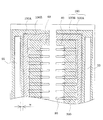
図1は、本発明の一実施形態に係るインクジェット式記録ヘッドの概略を示す分解斜視図であり、図2は、図1の平面図及びA−A′断面図であり、図3は、下電極膜及び独立電極層のパターンを示す平面図である。
Hereinafter, the present invention will be described in detail based on an embodiment.
FIG. 1 is an exploded perspective view showing an outline of an ink jet recording head according to an embodiment of the present invention, FIG. 2 is a plan view and a sectional view taken along line AA ′ of FIG. 1, and FIG. It is a top view which shows the pattern of an electrode film and an independent electrode layer.
図示するように、液体噴射ヘッドの一例であるインクジェット式記録ヘッドを構成する流路形成基板10は、本実施形態では面方位(110)のシリコン単結晶基板からなり、その一方の面には二酸化シリコンからなる弾性膜50が形成されると共に、圧力発生室12を含む第1のインク流路が形成されている。まず流路形成基板10には、隔壁11によって区画される複数の圧力発生室12がその幅方向に沿って並設された列が2列設けられている。また流路形成基板10の各圧力発生室12の列の外側には、隔壁11によって区画され各圧力発生室12に連通するインク供給路13と連通路14とがそれぞれ設けられている。さらに連通路14の外側には、各連通路14と連通する連通部15が設けられている。この連通部15は、後述する保護基板のリザーバ部と連通して、各列の圧力発生室12に共通するリザーバの一部を構成する。
As shown in the drawing, a flow
インク供給路13は、圧力発生室12よりも狭い断面積となるように形成されており、連通部15から圧力発生室12に流入するインクの流路抵抗を一定に保持している。例えば、本実施形態では、インク供給路13は、流路の幅を片側から絞ることで、圧力発生室12の幅より小さい幅で形成されている。各連通路14は、圧力発生室12の幅方向両側の隔壁11を連通部15側に延設してインク供給路13と連通部15との間の空間を区画することで形成されている。
The
なお、本実施形態では、流路の幅を片側から絞ることでインク供給路を形成したが、流路の幅を両側から絞ることでインク供給路を形成してもよい。 In this embodiment, the ink supply path is formed by narrowing the width of the flow path from one side. However, the ink supply path may be formed by narrowing the width of the flow path from both sides.
流路形成基板10の材料として、本実施形態ではシリコン単結晶基板を用いているが、勿論これに限定されず、例えば、ガラスセラミックス、ステンレス鋼等を用いてもよい。
As a material for the flow
流路形成基板10の開口面側には、各圧力発生室12のインク供給路13とは反対側の端部近傍に連通するノズル開口21が穿設されたノズルプレート(ノズル形成部材の一種)20が接着剤や熱溶着フィルム等を介して固着されている。ノズルプレート20の材料としては、例えば、ガラスセラミックス、シリコン単結晶基板又はステンレス鋼(SUS)等が挙げられるが、本実施形態では、ステンレス鋼を用いている。
A nozzle plate (a kind of nozzle forming member) in which a nozzle opening 21 communicating with the vicinity of the end of each
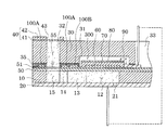
一方、このような流路形成基板10の開口面とは反対側には、上述したように弾性膜50が形成され、この弾性膜50上には、絶縁体膜51が形成されている。さらに、この絶縁体膜51上には、下電極膜60、圧電体層70及び上電極膜80からなる圧電素子300が形成されている。一般的には、圧電素子300の何れか一方の電極を共通電極とし、他方の電極を圧電体層70と共に圧力発生室12毎にパターニングして個別電極とする。本実施形態では、下電極膜60を圧電素子300の共通電極とし、上電極膜80を圧電素子300の個別電極としているが、駆動回路や配線の都合でこれを逆にしても支障はない。なお、上述した例では、弾性膜50、絶縁体膜51及び下電極膜60が実質的に振動板として作用するが、弾性膜50及び絶縁体膜51のみが振動板として機能するようにしてもよいし、弾性膜50及び絶縁体膜51を設けずに、下電極膜60のみが振動板として機能するようにしてもよい。
On the other hand, the
また流路形成基板10上には、圧電素子300を保護するための圧電素子保持部31を有する接合基板である保護基板30が接着剤35によって接合されている。圧電素子保持部31は、本実施形態では、各圧力発生室12の列毎に設けられている。なお、これらの圧電素子保持部31は密封されていてもよいが、密封されていなくてもよい。また保護基板30の各圧電素子保持部31の外側には、第2のインク流路であるリザーバ部32がそれぞれ形成されている。これらの各リザーバ部32は、弾性膜50及び絶縁体膜51を貫通して設けられる開口部55を介して流路形成基板10の各連通部15と連通されて、列毎の各圧力発生室12に共通するリザーバ150を構成している。さらに、保護基板30の各圧電素子保持部31の間、すなわち、保護基板30の中央部には、保護基板30を厚さ方向に貫通する接続孔33が設けられている。
On the flow
保護基板30上には、剛性が低く可撓性を有する材料で形成される封止膜41と金属等の硬質の材料で形成される固定板42とからなるコンプライアンス基板40が接合されている。なお、固定板42のリザーバ150に対向する領域は、厚さ方向に完全に除去された開口43となっており、リザーバ150の一方面は封止膜41のみで封止されている。
On the
ここで、各圧電素子300の個別電極である上電極膜80には、例えば、金(Au)等からなるリード電極90がそれぞれ接続されている。このリード電極90は、各圧電素子300の長手方向のインク供給路13とは反対側の端部近傍から引き出され、絶縁体膜51上を流路形成基板10の中央部近傍までそれぞれ延設されている。すなわち、リード電極90は、圧電素子保持部31内から接続孔33に対向する領域まで延設されている。また、圧電素子300の共通電極である下電極膜60は、各圧力発生室12に対向する領域に、圧力発生室12の並設方向に亘って連続的に延設されている。そして、下電極膜60は、圧力発生室12の列の外側で、リード電極90と同様に、保護基板30に設けられた接続孔33に対向する領域まで延設されている。そして、このように延設されたリード電極90及び下電極膜60は、図示しないが、接続孔33内に延設されるボンディングワイヤからなる接続配線によって、例えば、保護基板30上に実装される駆動ICと接続される。
Here,
また、圧力発生室12の列の外側に領域の絶縁体膜51上には、圧電素子300の上電極膜80及び下電極膜60とは独立した独立電極層100(第1の独立電極層100A、第2の独立電極層100B)が設けられている(図3参照)。この独立電極層100は、基本的には保護基板30が接合される接合領域内に設けられており接着剤35によって覆われている。なお、圧電素子300の上電極膜80及び下電極膜60と独立しているとは、これら上電極膜80及び下電極膜60と独立電極層100とが電気的に接続されていない状態をいう。勿論、独立電極層100は、上電極膜80から引き出されたリード電極90とも独立して設けられている。
The independent electrode layer 100 (first
詳細には、流路形成基板10の連通部15に対向する領域の弾性膜50及び絶縁体膜51には、連通部15とリザーバ部32とを連通させる開口部55の周縁部に、第1の独立電極層100Aが設けられている。第1の独立電極層100Aは、開口部55の端面から近接して設けられているが、第1の独立電極層100Aの端面が開口部55の端面とは一致しないように設けられている。
More specifically, the
インク供給路13及び連通路14に対向する領域の絶縁体膜51上、すなわち、第1の独立電極層100Aと下電極膜60との間の領域の絶縁体膜51上には、第2の独立電極層100Bがさらに設けられている。この第2の独立電極層100Bは、下電極膜60及び上電極膜80と電気的に独立していると共に、第1の独立電極層100Aとも電気的に独立して設けられている。
On the
これら第1及び第2の独立電極層100A,100Bは、上述したように接着剤35によって覆われているが、下電極膜60と同様に圧力発生室12の列の外側の領域で保護基板30の接続孔33に対向する領域まで延設され、各先端部が接続孔33内に露出されている。
The first and second
また、これら第1及び第2の独立電極層100A,100Bは、本実施形態では、下電極膜60と同一層からなり、下電極膜60をパターニングする際に同時に形成される。なお、第1及び第2の独立電極層100A,100Bは、必ずしも下電極膜60と同一の層で形成されている必要はなく、例えば、リード電極90と同一の層で形成されていてもよいし、下電極膜60及びリード電極90とは別途設けられていてもよい。
Further, in the present embodiment, the first and second
このような本実施形態のインクジェット式記録ヘッドは、図示しない外部インク供給手段からインクを取り込み、リザーバ150からノズル開口21に至るまで内部をインクで満たした後、図示しない駆動回路からの記録信号に従い、外部配線を介して圧力発生室12に対応するそれぞれの下電極膜60と上電極膜80との間に電圧を印加して圧電素子300を駆動することで、振動板を構成する弾性膜50及び絶縁体膜51をたわみ変形させることにより、各圧力発生室12内の圧力が高まりノズル開口21からインク滴が吐出する。
Such an ink jet recording head of this embodiment takes in ink from an external ink supply means (not shown), fills the interior from the
以下、このような本実施形態のインクジェット式記録ヘッドの製造方法及び検査方法の一例について、図4〜図7の流路形成基板の圧力発生室12の長手方向の一部を示す断面図を参照して説明する。なお、図4〜図6は、記録ヘッドの製造工程を示す図であり、図7は、記録ヘッドの導通検査工程を示す図である。
Hereinafter, for an example of the manufacturing method and the inspection method of the ink jet recording head according to this embodiment, refer to cross-sectional views showing a part in the longitudinal direction of the
まず、図4(a)に示すように、シリコンウェハであり流路形成基板10が複数一体的に形成される流路形成基板用ウェハ110の表面に弾性膜50を構成する二酸化シリコン膜52を形成する。次に、図4(b)に示すように、弾性膜50上に、弾性膜50とは異なる材料の酸化膜からなる絶縁体膜51を形成する。
First, as shown in FIG. 4A, a
次いで、図4(c)に示すように、絶縁体膜51上の全面に第1の金属膜160を形成し、この第1の金属膜160をパターニングすることによって、下電極膜60、第1及び第2の独立電極層100A,100Bを形成する。次に、図3(d)に示すように、例えば、チタン酸ジルコン酸鉛(PZT)等からなる圧電材料層170と、第2の金属膜180とを流路形成基板用ウェハ110の全面に形成し、これら圧電材料層170及び第2の金属膜180とを、各圧力発生室12に対向する領域にパターニングして下電極膜60、圧電体層70及び上電極膜80からなる圧電素子300を形成する。
Next, as shown in FIG. 4C, a
次に、図4(e)に示すように、流路形成基板用ウェハ110の全面に亘って、第3の金属膜190を形成し、この金属膜190を各圧電素子300毎にパターニングすることによってリード電極90を形成する。
Next, as shown in FIG. 4E, a
次いで、複数の保護基板30が一体的に形成されるシリコンウェハからなる保護基板用ウェハ130を、図5(a)に示すように、流路形成基板用ウェハ110上に、接着剤35、例えば、エポキシ系の接着剤によって接合する。
Next, a
次いで、図5(b)に示すように、流路形成基板用ウェハ110をある程度の厚さまで薄くした後、図6(a)に示すように、流路形成基板用ウェハ110上に、例えば、保護膜53を新たに形成して所定形状にパターニングする。そして、図6(b)に示すように、この保護膜53をマスクとして流路形成基板用ウェハ110を異方性エッチング(ウェットエッチング)して、流路形成基板用ウェハ110に圧力発生室12、インク供給路13、連通路14及び連通部15を形成する。すなわち、流路形成基板用ウェハ110を、例えば、水酸化カリウム(KOH)水溶液等のエッチング液によって、弾性膜50が露出するまで流路形成基板用ウェハ110をエッチングすることより、圧力発生室12等を同時に形成する。また、弾性膜50及び絶縁体膜51を除去して開口部55を形成して、連通部15とリザーバ部32とを連通させる。
Next, as shown in FIG. 5 (b), after the flow path forming
その後は、流路形成基板用ウェハ110及び保護基板用ウェハ130の外周縁部の不要部分を、例えば、ダイシング等により切断することによって除去する。そして、流路形成基板用ウェハ110の保護基板用ウェハ130とは反対側の面に、ノズル開口21が穿設されたノズルプレート20を接合すると共に、保護基板用ウェハ130にコンプライアンス基板40を接合する。そして、これら流路形成基板用ウェハ110、保護基板用ウェハ130等を一つのチップサイズの流路形成基板10等に分割する(図2参照)。
Thereafter, unnecessary portions of the outer peripheral edge portions of the flow path forming
このような状態で、次に導通検査工程を実施する。具体的には、図7に示すように、インク流路、すなわち、リザーバ150から圧力発生室12まで導電性液体、例えば、インクを充填し、この状態で下電極膜60、第1の独立電極層100A及び第2の独立電極層100Bと、導電性液体との間での導通状態をそれぞれ検出する。本実施形態では、ノズルプレート20が、導電性を有する材料で形成されているため、下電極膜60、第1及び第2の独立電極層100A,100Bとノズルプレート20との間で導通状態を検出するようにした。導通状態の検出方法は、特に限定されないが、例えば、所定のプローブピン200を、接続孔33内に露出された下電極膜60、第1及び第2の独立電極層100A,100Bとノズルプレート20とにそれぞれ接触させて両プローブピン200間の抵抗値等を測定すればよい。そして、この測定結果から接続孔33内に露出された下電極膜60、第1及び第2の独立電極層100A,100Bとノズルプレート20との間が導通状態であるか絶縁状態であるかを判定し、絶縁状態と判定されたインクジェット式記録ヘッドのみを良品、すなわち製品とする。
In this state, a continuity inspection process is performed next. Specifically, as shown in FIG. 7, the ink flow path, that is, the
このように本実施形態では、インクジェット式記録ヘッドを製造する際に、圧電素子300を構成する下電極膜60とは独立する独立電極層100(第1及び第2の独立電極層100A,100B)とを設けておき、導通検査工程で、下電極膜60及び独立電極層100と、ノズルプレート20との間の導通状態を検出するようにした。これにより、例えば、振動板を構成する弾性膜50及び絶縁体膜51の割れや、接着剤35の接着不良等による製造不良を容易且つ確実に検出することができる。弾性膜50及び絶縁体膜51に割れが発生していたり、接着剤35の接着不良が生じていたりするとインクが漏れ出し、下電極膜60、第1及び第2の独立電極層100A,100Bと、ノズルプレート20との間が導通状態となる。このため、導通検査工程を実施することで、このような不良の発生を容易且つ確実に検出することができ、ユーザ使用時の初期不良の発生を大幅に削減することができる。
As described above, in the present embodiment, when the ink jet recording head is manufactured, the independent electrode layer 100 (first and second
また、下電極膜60とノズルプレート20間の導通状態と共に、独立電極層100とノズルプレート20との間の導通状態を検出することで、不良の発生位置及び原因を特定することができる。具体的には、ノズルプレート20と、下電極膜60、第1の独立電極層100A又は第2の独立電極層100Bの何れとの間が導通状態となっているかによって、不良の発生位置をある程度特定することができる。さらに、下電極膜60又は第2の独立電極層100Bとノズルプレート20との間が導通状態であれば、振動板の割れによるものと判断することができ、一方、第1の独立電極層100Aとノズルプレート20との間が導通状態であれば、接着剤35の接着不良によるものと判断することができる。このように不良の発生位置及び発生原因を特定することで、発生した不良への適切な対策を講じることができるようになる。
Further, by detecting the conduction state between the
なお、このように発生原因を特定するという観点からは、第1の独立電極層100Aの開口部55に沿った部分の幅を可及的に細く形成しておくことが好ましい。特に、第2の独立電極層100Bに隣接する部分、つまり、連通路14に対向する領域の第1の独立電極層100Aの幅W(図2参照)を可及的に細く形成しておくことが好ましい。これにより、不良の発生原因が、振動板の割れであるか、接着不良であるかをより正確に判断することができる。
From the viewpoint of specifying the cause of occurrence in this way, it is preferable to form the width of the portion along the
(他の実施形態)
以上、本発明の実施形態について説明したが、勿論、本発明は、この実施形態に限定されるものではない。例えば、上述の実施形態では、下電極膜60、第1及び第2の独立電極層100A,100Bとノズルプレート20との間の導通状態を検出するようにしたが、これに限定されず、下電極膜60、第1及び第2の独立電極層100A,100Bと導電性液体(インク)との間の導通状態を直接検出するようにしてもよい。また、上述の実施形態では、下電極膜60と第1の独立電極層100Aとの間に、第2の独立電極層100Bを設けるようにしたが、この第2の独立電極層100Bは設けられていなくてもよく、また第2の独立電極層100Bは、上電極膜80と電気的に独立していれば良く、下電極膜60から連続して形成されていてもよい。
(Other embodiments)
As mentioned above, although embodiment of this invention was described, of course, this invention is not limited to this embodiment. For example, in the above-described embodiment, the conduction state between the
なお、上述した実施形態においては、液体噴射ヘッドの一例としてインクジェット式記録ヘッドを挙げて説明したが、本発明は、広く液体噴射ヘッド全般を対象としたものであり、インク以外の液体を噴射する液体噴射ヘッドを検査する場合にも勿論適用することができる。その他の液体噴射ヘッドとしては、例えば、プリンタ等の画像記録装置に用いられる各種の記録ヘッド、液晶ディスプレー等のカラーフィルタの製造に用いられる色材噴射ヘッド、有機ELディスプレー、FED(電界放出ディスプレー)等の電極形成に用いられる電極材料噴射ヘッド、バイオchip製造に用いられる生体有機物噴射ヘッド等が挙げられる。 In the above-described embodiment, an ink jet recording head has been described as an example of a liquid ejecting head. However, the present invention is widely intended for all liquid ejecting heads and ejects liquids other than ink. Of course, the present invention can also be applied to the case of inspecting the liquid jet head. Other liquid ejecting heads include, for example, various recording heads used in image recording apparatuses such as printers, color material ejecting heads used in the manufacture of color filters such as liquid crystal displays, organic EL displays, and FEDs (field emission displays). Examples thereof include an electrode material ejection head used for electrode formation, a bioorganic matter ejection head used for biochip production, and the like.
10 流路形成基板、 12 圧力発生室、 13 インク供給路、 14 連通路、 15 連通部、 20 ノズルプレート、 21 ノズル開口、 30 保護基板、 31 圧電素子保持部、 32 リザーバ部、 33 接続孔、 35 接着剤、 40 コンプライアンス基板、 50 弾性膜、 51 絶縁体膜、 55 開口部、 60 下電極膜、 70 圧電体層、 80 上電極膜、 90 リード電極、 100 独立電極層、 300 圧電素子
DESCRIPTION OF
Claims (4)
前記流路形成基板上に前記圧電素子を形成する際に、前記圧電素子の前記下電極膜及び前記上電極膜とは電気的に独立する第1の独立電極層を前記振動板上の少なくとも前記開口部の周縁部に形成しておき、
前記液体噴射ヘッドの前記第1及び第2の液体流路内に導電性液体を充填した状態で、前記圧電素子の下電極膜及び前記第1の独立電極層と、前記導電性液体との間での導通状態をそれぞれ検出する導通検査工程を実施することを特徴とする液体噴射ヘッドの検査方法。 A flow path forming substrate having a first liquid flow path including a pressure generating chamber communicating with a nozzle for discharging droplets, a lower electrode film provided on one surface side of the flow path forming substrate via a vibration plate, and piezoelectric A piezoelectric element composed of a body layer and an upper electrode film, and a first element connected to the one surface side of the flow path forming substrate by an adhesive and communicated with the first liquid flow path through an opening provided in the diaphragm. An inspection method for a liquid jet head having a bonding substrate having two liquid flow paths,
When forming the piezoelectric element on the flow path forming substrate, at least the first independent electrode layer electrically independent from the lower electrode film and the upper electrode film of the piezoelectric element is provided on the diaphragm. Formed on the periphery of the opening,
Between the lower electrode film and the first independent electrode layer of the piezoelectric element and the conductive liquid in a state where the first and second liquid flow paths of the liquid jet head are filled with the conductive liquid. A method for inspecting a liquid ejecting head, comprising performing a continuity inspection step of detecting a continuity state in each.
前記導通検査工程では、前記下電極膜及び前記第1の独立電極層と、前記ノズル形成部材との間での導通状態をそれぞれ検出することを特徴とする請求項1に記載の液体噴射ヘッドの検査方法。 The liquid ejecting head includes a nozzle forming member made of a conductive material and joined to the other surface side of the flow path forming substrate.
2. The liquid ejecting head according to claim 1, wherein in the continuity inspection step, a continuity state between the lower electrode film and the first independent electrode layer and the nozzle forming member is detected. Inspection method.
前記導通検出工程では、前記第2の独立電極層と、前記導電性液体との間での導通状態をさらに検出するようにしたことを特徴とする請求項1又は2に記載の液体噴射ヘッドの検査方法。 When forming the piezoelectric element on the flow path forming substrate, a second independent electrode layer that is electrically independent from the lower electrode film, the upper electrode film, and the first independent electrode layer, Further provided in a region facing the first liquid flow path between one independent electrode layer and the lower electrode film,
3. The liquid ejecting head according to claim 1, wherein in the conduction detecting step, a conduction state between the second independent electrode layer and the conductive liquid is further detected. Inspection method.
Priority Applications (1)
| Application Number | Priority Date | Filing Date | Title |
|---|---|---|---|
| JP2007064075A JP2008221652A (en) | 2007-03-13 | 2007-03-13 | Method for inspecting liquid jet head |
Applications Claiming Priority (1)
| Application Number | Priority Date | Filing Date | Title |
|---|---|---|---|
| JP2007064075A JP2008221652A (en) | 2007-03-13 | 2007-03-13 | Method for inspecting liquid jet head |
Publications (2)
| Publication Number | Publication Date |
|---|---|
| JP2008221652A true JP2008221652A (en) | 2008-09-25 |
| JP2008221652A5 JP2008221652A5 (en) | 2010-02-12 |
Family
ID=39840810
Family Applications (1)
| Application Number | Title | Priority Date | Filing Date |
|---|---|---|---|
| JP2007064075A Withdrawn JP2008221652A (en) | 2007-03-13 | 2007-03-13 | Method for inspecting liquid jet head |
Country Status (1)
| Country | Link |
|---|---|
| JP (1) | JP2008221652A (en) |
Cited By (6)
| Publication number | Priority date | Publication date | Assignee | Title |
|---|---|---|---|---|
| JP2008221686A (en) * | 2007-03-14 | 2008-09-25 | Brother Ind Ltd | Liquid ejection head checking method and manufacturing method |
| JP2010221577A (en) * | 2009-03-24 | 2010-10-07 | Brother Ind Ltd | Liquid discharge device |
| JP2011167964A (en) * | 2010-02-19 | 2011-09-01 | Seiko Epson Corp | Liquid ejection head |
| US8393717B2 (en) | 2009-08-04 | 2013-03-12 | Seiko Epson Corporation | Liquid ejecting head and method of inspecting liquid ejecting head |
| JP2013146886A (en) * | 2012-01-18 | 2013-08-01 | Seiko Epson Corp | Liquid ejection head and liquid ejection device |
| KR20210082942A (en) * | 2019-12-26 | 2021-07-06 | 한국기계연구원 | Inkjet head and inkjet printer |
-
2007
- 2007-03-13 JP JP2007064075A patent/JP2008221652A/en not_active Withdrawn
Cited By (8)
| Publication number | Priority date | Publication date | Assignee | Title |
|---|---|---|---|---|
| JP2008221686A (en) * | 2007-03-14 | 2008-09-25 | Brother Ind Ltd | Liquid ejection head checking method and manufacturing method |
| JP4582104B2 (en) * | 2007-03-14 | 2010-11-17 | ブラザー工業株式会社 | Inspection method and manufacturing method of liquid discharge head |
| JP2010221577A (en) * | 2009-03-24 | 2010-10-07 | Brother Ind Ltd | Liquid discharge device |
| US8393717B2 (en) | 2009-08-04 | 2013-03-12 | Seiko Epson Corporation | Liquid ejecting head and method of inspecting liquid ejecting head |
| JP2011167964A (en) * | 2010-02-19 | 2011-09-01 | Seiko Epson Corp | Liquid ejection head |
| JP2013146886A (en) * | 2012-01-18 | 2013-08-01 | Seiko Epson Corp | Liquid ejection head and liquid ejection device |
| KR20210082942A (en) * | 2019-12-26 | 2021-07-06 | 한국기계연구원 | Inkjet head and inkjet printer |
| KR102400052B1 (en) * | 2019-12-26 | 2022-05-19 | 한국기계연구원 | Inkjet head and inkjet printer |
Similar Documents
| Publication | Publication Date | Title |
|---|---|---|
| JP2008221652A (en) | Method for inspecting liquid jet head | |
| JP5321831B2 (en) | Liquid ejecting head and manufacturing method thereof | |
| JP4221611B2 (en) | Method for manufacturing liquid jet head | |
| JP5977923B2 (en) | Liquid ejecting head, manufacturing method thereof, and liquid ejecting apparatus | |
| JP2007194373A (en) | Manufacturing method of silicon device and manufacturing method of liquid injection head | |
| JP2009184213A (en) | Liquid jetting head unit | |
| JP4849240B2 (en) | Method for manufacturing liquid jet head and liquid jet head | |
| JP6708015B2 (en) | MEMS device, liquid ejecting head, liquid ejecting apparatus, and method for manufacturing MEMS device | |
| JP4572371B2 (en) | Functional device, manufacturing method thereof, and liquid jet head | |
| JP2007245660A (en) | Manufacturing method of metal wiring board and manufacturing method of liquid jet head | |
| JP2017042952A (en) | Electronic device, piezoelectric device, liquid injection head and manufacturing method for the same | |
| JP2009190339A (en) | Liquid jet head and its manufacturing method | |
| JP2004066538A (en) | Liquid ejection head, its inspecting method and manufacturing process | |
| JP2013121694A (en) | Circuit member, head and device for ejecting liquid | |
| JP2011207072A (en) | Method for manufacturing liquid jet head | |
| JP2007216433A (en) | Penetration method and manufacturing method for liquid jet head | |
| JP2009208382A (en) | Liquid jet head and manufacturing method therefor | |
| JP2007098659A (en) | Penetration method and method for manufacturing liquid jet head | |
| JP2008194985A (en) | Manufacturing method of liquid ejection head | |
| JP2011073357A (en) | Liquid jetting head, liquid jetting apparatus, and method for manufacturing liquid jetting head | |
| JP2009126020A (en) | Method for inspecting liquid injection head | |
| JP5024824B2 (en) | Head abnormality detection method | |
| JP2005169874A (en) | Method of inspecting liquid jet head | |
| JP2008168549A (en) | Method for manufacturing liquid jetting head | |
| TW202030096A (en) | Fluidic device with nozzle layer conductors |
Legal Events
| Date | Code | Title | Description |
|---|---|---|---|
| A521 | Written amendment |
Effective date: 20091218 Free format text: JAPANESE INTERMEDIATE CODE: A523 |
|
| A621 | Written request for application examination |
Effective date: 20091218 Free format text: JAPANESE INTERMEDIATE CODE: A621 |
|
| A977 | Report on retrieval |
Free format text: JAPANESE INTERMEDIATE CODE: A971007 Effective date: 20111125 |
|
| A761 | Written withdrawal of application |
Free format text: JAPANESE INTERMEDIATE CODE: A761 Effective date: 20111205 |