JP2008216425A - Electrooptical device, driving method, and electronic equipment - Google Patents
Electrooptical device, driving method, and electronic equipment Download PDFInfo
- Publication number
- JP2008216425A JP2008216425A JP2007051226A JP2007051226A JP2008216425A JP 2008216425 A JP2008216425 A JP 2008216425A JP 2007051226 A JP2007051226 A JP 2007051226A JP 2007051226 A JP2007051226 A JP 2007051226A JP 2008216425 A JP2008216425 A JP 2008216425A
- Authority
- JP
- Japan
- Prior art keywords
- voltage
- signal
- data
- scanning
- line
- Prior art date
- Legal status (The legal status is an assumption and is not a legal conclusion. Google has not performed a legal analysis and makes no representation as to the accuracy of the status listed.)
- Withdrawn
Links
Images


Abstract
Description
本発明は、電気光学装置において、いわゆる縦クロストーク等の発生を抑える技術に関する。 The present invention relates to a technique for suppressing the occurrence of so-called vertical crosstalk in an electro-optical device.
近年では、液晶装置のような電気光学装置を用いて所定の画像を形成し、形成した画像を光学系によって拡大投射するプロジェクタが普及しつつある。このような電気光学装置では、複数行の走査線と複数列のデータ線との交差に対応して画素が複数設けられ、各画素は、液晶容量と、薄膜トランジスタ(thin film transistor:以下「TFT」と称する)のようなスイッチング素子とを有し、液晶容量は、画素電極と対向電極とで液晶を挟持して保持電圧に応じて透過率(反射率)が変化し、TFTは、走査線に選択電圧が印加したときにデータ線と画素電極との間でオン状態となる。
このため、複数行の走査線を順番に選択して、選択した走査線に選択電圧を印加して、TFTをオンさせるとともに、選択走査線に位置する画素電極に対し、階調(明るさ)に応じた電圧のデータ信号を、データ線およびオン状態のTFTを介して供給すると、各液晶容量に対しデータ信号に応じた電圧を保持させることができるので、所定の画像を形成することが可能となる。
ここで、プロジェクタに適用される電気光学装置では、画素間が非常に狭いので、いわゆるディスクリネーション(配向不良)が問題となるが、このディスクリネーションについては、隣接画素同士を互いに同一極性とする面反転方式を採用することで回避することができる(特許文献1参照)。
Therefore, a plurality of scanning lines are sequentially selected, a selection voltage is applied to the selected scanning lines, the TFT is turned on, and a gradation (brightness) is applied to the pixel electrode positioned on the selected scanning line. When a data signal having a voltage corresponding to the voltage is supplied via the data line and the on-state TFT, the voltage corresponding to the data signal can be held in each liquid crystal capacitor, so that a predetermined image can be formed. It becomes.
Here, in the electro-optical device applied to the projector, since the distance between the pixels is very narrow, so-called disclination (orientation failure) is a problem. However, with regard to this disclination, adjacent pixels have the same polarity. This can be avoided by adopting a surface reversal method (see Patent Document 1).
しかしながら、この面反転方式では、例えば灰色を背景として黒色領域をウィンドウ表示させようとする場合、図8(a)に示されるように、黒色領域の上および下側の灰色領域が、他の灰色領域の明るさと異なってしまう現象が発生する。この現象は、明るさの異なる領域が縦方向に現れるので、縦クロスロークと呼ばれることがある。
本発明は、上述した事情に鑑みてなされたもので、その目的とするところは、このような縦クロストークの発生を抑えた電気光学装置、駆動方法および電子機器を提供することにある。
However, in this surface inversion method, for example, when displaying a black region in a window with a gray background, as shown in FIG. 8A, the gray region above and below the black region is replaced with another gray region. A phenomenon occurs that differs from the brightness of the area. This phenomenon is sometimes called a vertical cross-roke because areas with different brightness appear in the vertical direction.
The present invention has been made in view of the above-described circumstances, and an object thereof is to provide an electro-optical device, a driving method, and an electronic apparatus in which occurrence of such vertical crosstalk is suppressed.
上記目的を達成するために本発明に係る電気光学装置の駆動方法にあっては、複数行の走査線と複数列のデータ線との交差に対応して設けられ、走査線に選択電圧を印加したときに、データ線に供給されるとともに所定電位を基準とした正極性電圧または負極性電圧に応じた階調となる複数の画素を備える電気光学装置の駆動方法であって、前記複数行の走査線を所定の順番で選択して、前記選択電圧を印加し、前記複数列のデータ線に対して、一の走査線に前記選択電圧を印加する前に、極性とは無関係の第1電圧を印加し、前記第1電圧の印加後に、前記正極性または前記負極性に応じた第2電圧を印加し、前記一の走査線に選択電圧を印加したときに、一のデータ線と前記一の走査線との交差に対応する画素の階調に応じ、かつ、前記第2電圧を印加したときの極性に応じた電圧を、前記一のデータ線に供給することを特徴とする。本発明によれば、複数列のデータ線に対して階調に応じた電圧を印加する前に、第1および第2電圧のプリチャージが2回実行される。このうち、第1電圧のプリチャージによってスイッチング素子のオフリークが促進し、第2電圧のプリチャージによって階調に応じた電圧を印加する前の初期状態が揃えられる。 In order to achieve the above object, the electro-optical device driving method according to the present invention is provided corresponding to the intersection of a plurality of scanning lines and a plurality of columns of data lines, and applies a selection voltage to the scanning lines. A driving method of an electro-optical device including a plurality of pixels that are supplied to a data line and have gradations according to a positive voltage or a negative voltage with reference to a predetermined potential, A scanning voltage is selected in a predetermined order, the selection voltage is applied, and before the selection voltage is applied to one scanning line with respect to the plurality of columns of data lines, a first voltage independent of polarity is applied. After the first voltage is applied, a second voltage corresponding to the positive polarity or the negative polarity is applied, and when a selection voltage is applied to the one scanning line, one data line and the one voltage are applied. According to the gradation of the pixel corresponding to the intersection with the scanning line, and A voltage corresponding to the polarity upon application of second voltage, and supplying to the one of the data lines. According to the present invention, the precharge of the first and second voltages is performed twice before applying the voltage corresponding to the gradation to the data lines in a plurality of columns. Among them, the off-leakage of the switching element is promoted by the precharge of the first voltage, and the initial state before applying the voltage corresponding to the gradation is made uniform by the precharge of the second voltage.
本発明において、前記画素は、画素電極と対向電極とで液晶を挟持した液晶容量と、走査線に印加されたときに、データ線と画素電極との間で導通状態となるスイッチング素子と、を有し、前記第1電圧は、前記データ線に供給される電圧範囲のうち、前記スイッチング素子が非導通状態であるときに、前記液晶容量のリークが最大となる電圧であることが好ましい。
また、本発明において、前記複数列のデータ線に前記第2電圧を印加するときに、前記一の走査線に選択電圧を印加しても良い。
なお、本発明は、電気光学装置の駆動方法のみならず、電気光学装置、さらには、当該電気光学装置を有する電子機器としても概念することが可能である。
In the present invention, the pixel includes a liquid crystal capacitor in which a liquid crystal is sandwiched between a pixel electrode and a counter electrode, and a switching element that is conductive between the data line and the pixel electrode when applied to the scanning line. Preferably, the first voltage is a voltage that maximizes leakage of the liquid crystal capacitance when the switching element is in a non-conducting state within a voltage range supplied to the data line.
In the present invention, when the second voltage is applied to the plurality of columns of data lines, a selection voltage may be applied to the one scanning line.
The present invention can be conceptualized not only as a method for driving an electro-optical device, but also as an electro-optical device, and also as an electronic apparatus having the electro-optical device.
以下、本発明の実施形態について図面を参照して説明する。 Embodiments of the present invention will be described below with reference to the drawings.
図1は、本実施形態に係る電気光学装置の構成を示すブロック図である。
この図に示されるように、電気光学装置10は、制御回路50と液晶表示パネル100とを含む。
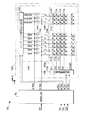
このうち、液晶表示パネル100は、表示領域100aの周辺に走査線駆動回路130およびデータ線駆動回路140を内蔵した周辺回路内蔵型となっている。表示領域100aでは、1080行の走査線112が行(X)方向に延在するように設けられ、また、1920列のデータ線114が列(Y)方向に延在するように、かつ、各走査線112と互いに電気的に絶縁を保つように設けられ、さらに、画素110が1080行の走査線112と1920列のデータ線114との交差に対応して、それぞれ配列している。したがって、本実施形態では、画素110が縦1080行×横1920列のマトリクス状に配列することになる。
FIG. 1 is a block diagram illustrating a configuration of the electro-optical device according to the present embodiment.
As shown in this figure, the electro-
Among these, the liquid
説明の便宜上、画素110の構成について図2を参照して説明する。図2は、i行及びこれと1行下で隣接する(i+1)行と、j列及びこれと1列右で隣接する(j+1)列との交差に対応する2×2の計4画素分の構成を示している。なお、i、(i+1)は、画素110が配列する行を一般的に示す場合の記号であって、この例では、1以上1080以下の整数である。また、j、(j+1)は、画素110が配列する列を一般的に示す場合の記号であって、この例では、1以上1920以下の整数である。
For convenience of description, the configuration of the
図2に示されるように、各画素110は、nチャネル型のTFT116と液晶容量120とを含む。
ここで、各画素110については互いに同一構成なので、i行j列に位置するもので代表させて説明すると、当該i行j列の画素110におけるTFT116のゲート電極はi行目の走査線112に接続される一方、そのソース電極はj列目のデータ線114に接続され、そのドレイン電極は液晶容量120の一端である画素電極118に接続されている。また、液晶容量120の他端は、対向電極108に接続されている。この対向電極108は、全ての画素110にわたって共通であって、本実施形態では、時間的に一定の電圧LCcomが印加されている。
As shown in FIG. 2, each
Here, since each
この液晶表示パネル100は、特に図示しないが、素子基板と対向基板との一対の基板が一定の間隙を保って貼り合わせられるとともに、この間隙に液晶が封止された構成となっている。このうち、素子基板には、走査線112や、データ線114、TFT116および画素電極118が走査線駆動回路130やデータ線駆動回路140とともに形成される一方、対向基板に対向電極108が形成されて、これらの電極形成面が互いに対向するように一定の間隙を保って貼り合わせられている。このため、本実施形態において液晶容量120は、画素電極118と対向電極108とで液晶105を挟持することによって構
成される。
なお、本実施形態では、液晶容量120において保持される電圧実効値がゼロに近ければ、液晶容量を通過する光の透過率が最大となって白色表示になる一方、電圧実効値が大きくなるにつれて透過率が減少して、ついには透過率が最小の黒色表示になるノーマリーホワイトモードに設定されている。
The liquid
In this embodiment, if the effective voltage value held in the
この構成において、走査線112に選択電圧を印加し、TFT116をオン(導通)させるとともに、画素電極118に、データ線114およびオン状態のTFT116を介して、階調(明るさ)に応じた電圧のデータ信号を供給すると、選択電圧を印加した走査線112とデータ信号を供給したデータ線114との交差に対応する液晶容量120に、階調に応じた電圧を書き込むことができる。
なお、走査線112が非選択電圧になると、TFT116がオフ(非導通)状態となるが、液晶容量120では、TFT116がオン状態となったときに書き込まれた電圧が、その容量性により保持される。
In this configuration, a selection voltage is applied to the
Note that when the
走査線駆動回路130は、それぞれ1、2、3、…、1080行目の走査線112を、それぞれこの順番で選択して、この選択に応じた走査信号G1、G2、G3、…、G1080を
、供給するものである。ここで、走査線駆動回路130は、選択した走査線への走査信号をHレベルに相当する電圧Vddとし、それ以外の走査線への走査信号をLレベルに相当する非選択電圧(接地電位Gnd)とする。
走査線駆動回路130の構成については、特に詳述しないが、簡単にいえば例えば図5に示されるように、垂直走査期間(F)の最初に供給されるスタートパルスDyを、クロ
ック信号Clyの論理レベルが遷移する(立ち下がり及び立ち上がる)毎に順番にシフト転送して、このシフト信号を走査信号として出力する構成である。
The scanning
Although the configuration of the scanning
データ線駆動回路140は、サンプリング信号出力回路142と、各データ線114にそれぞれ設けられたOR回路144およびnチャネル型のTFT146の組とによって構成される。サンプリング信号出力回路142は、各行の走査線112が選択される水平走査期間にわたって、順次排他的にHレベルとなるサンプリング信号S1、S2、S3、…、
S1920を出力するものである。
なお、サンプリング信号出力回路142の構成については、特に詳述しないが、簡単にいえば例えば図6に示されるように、水平走査期間(H)の最初に供給されるスタートパルスDxを、クロック信号Clxの論理レベルが遷移する毎に順番にシフト転送して、この
シフト信号をサンプリング信号として出力する構成である。
The data
S1920 is output.
The configuration of the sampling
OR回路144は、サンプリング信号とプリチャージ指定信号Nrgとの論理和信号を求めるものである。TFT146は、そのソース電極が画像信号線148に接続され、そのドレイン電極がデータ線114に接続されて、そのゲート電極には、サンプリング信号が供給される。例えばj列目のOR回路144は、サンプリング信号Sjとプリチャージ指
定信号Nrgとの論理和信号を求めて、j列目のTFT146のゲート電極に供給する。また、j列目のTFT146のドレイン電極がj列目のデータ線114に接続されている。
したがって、j列目のTFT146は、サンプリング信号SjがHレベルになると、ま
たは、プリチャージ指定信号NrgがHレベルになると、オン状態になって、画像信号線148に供給されたデータ信号Vidを、j列目のデータ線114にサンプリングすることになる。
The OR
Therefore, the
説明を再び図1に戻すと、制御回路50は、走査線駆動回路130およびデータ線駆動回路140を制御するとともに、これらの制御に合わせて画像信号線148にデータ信号Vidを供給するものである。
Returning to FIG. 1 again, the
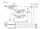
図3は、制御回路50の構成を示すブロック図である。
制御回路50には、図示しない上位回路から画像データVdが、垂直同期信号Vs、水平同期信号Hsおよびクロック信号Clkに同期して供給される。ここで、画像データVdは、縦1080行×横1920列の画素110の階調を例えば8ビットで指定するデジタルデータであり、図4に示されるように、垂直同期信号Vsで規定される垂直走査期間(F)
にわたって、1行1列〜1行1920列、2行1列〜2行1920列、3行1列〜3行1920列、…、1080行1列〜1080行1920列という画素の順番で供給される。この供給の際に、水平同期信号Hsで規定される水平走査期間(H)において1行分の画
像データVdが供給され、さらに、クロック信号Clkの1周期で1画素分の画像データVdが供給される。
FIG. 3 is a block diagram showing a configuration of the
Image data Vd is supplied to the
1 row, 1 column to 1 row, 1920 column, 2 rows, 1 column to 2 rows, 1920 columns, 3 rows, 1 column to 3 rows, 1920 columns,..., 1080 rows, 1 column to 1080 rows, 1920 columns are supplied in this order. The At the time of this supply, one row of image data Vd is supplied in the horizontal scanning period (H) defined by the horizontal synchronizing signal Hs, and one pixel of image data Vd is supplied in one cycle of the clock signal Clk. Is done.
なお、図4において、水平帰線期間Hbとは、ある水平走査期間において、最終192
0列の画素の画像データVdが供給終了してから、次の水平走査期間において1列の画素
の画像データVdが供給開始されるまでの期間をいう。
また、ある垂直走査期間において最終行最終列である1080行1920列の画素の画像データVdが供給終了してから、次の垂直走査期間において1行1列の画素の画像デー
タVdが供給開始されるまでの期間を、特に垂直帰線期間という場合もあるが、本説明で
は、水平帰線期間として区別していない。
本実施形態において8ビットの画像データVdは、十進表記の「0」が最低階調の黒色
を指定し、数値が増加するにつれて明るくなる階調を指定し、「255」が最高階調の白色を指定するものとする。上述したように本実施形態ではノーマリーホワイトモードに設定されているので、階調値「255」で指定された白色とする場合には、液晶容量120で保持される電圧の実効値をゼロ近傍とし、階調値「0」で指定された黒色とする場合には、液晶容量120で保持される電圧の実効値を最高値とすれば良いことになる。
In FIG. 4, the horizontal blanking period Hb is the last 192 in a horizontal scanning period.
This is a period from the end of the supply of the image data Vd of the pixels in the 0th column to the start of the supply of the image data Vd of the pixels in the first column in the next horizontal scanning period.
In addition, after the supply of image data Vd of pixels of 1080 rows and 1920 columns, which is the final row and final column, is completed in a certain vertical scanning period, supply of image data Vd of pixels of 1 row and 1 column is started in the next vertical scanning period. This period is sometimes referred to as a vertical blanking period, but in this description, it is not distinguished as a horizontal blanking period.
In the present embodiment, the 8-bit image data Vd specifies “0” in decimal notation to specify black with the lowest gradation, specifies a gradation that becomes brighter as the numerical value increases, and “255” indicates the highest gradation. White color shall be specified. As described above, since the normally white mode is set in the present embodiment, when the white color specified by the gradation value “255” is set, the effective value of the voltage held in the
走査制御回路52は、垂直同期信号Vs、水平同期信号Hsおよびクロック信号Clkに同期して、スタートパルスDx、Dyおよびクロック信号Clx、Clyを出力する。
詳細には、画像データVdが図4に示されるように供給される場合に、走査制御回路5
2は、1行目の画像データVdが供給される水平走査期間(H)に1行目の走査線112
が選択されるように、同様に、2、3、4、…、1080行の画像データVdが供給され
る水平走査期間(H)にそれぞれ2、3、4、…、1080行目の走査線112が選択されるように、スタートパルスDyおよびクロック信号Clyを出力して走査線駆動回路13
0を制御する。
さらに、走査制御回路52は、ある走査線112が選択される水平走査期間(H)において、1列目の画像データVdが供給されるときにサンプリング信号S1がHレベルとなるように、同様に、2、3、4、…、1920列目の画像データVdが供給されるときにそ
れぞれサンプリング信号S2、S3、S4、…、S1920がHレベルとなるように、スタート
パルスDxおよびクロック信号Clxを出力してサンプリング信号出力回路142を制御す
る。
The
More specifically, when the image data Vd is supplied as shown in FIG.
2 shows a
Similarly, the second, third, fourth,..., 1080th scanning lines in the horizontal scanning period (H) during which the second, third, fourth,... 1080th image data Vd is supplied. The scan line drive circuit 13 outputs the start pulse Dy and the clock signal Cly so that 112 is selected.
Control 0.
Further, the
走査制御回路52は、また、極性指定信号Pol、プリチャージ指定信号Nrgおよび信号Praを出力する。このうち、極性指定信号Polは、液晶容量120に対する電圧の書込極性を指定する信号であり、例えばHレベルであれば正極性を、Lレベルであれば負極性を、それぞれ指定する。ここで、正極性とは、対向電極108への印加電圧LCcomよりも
やや高位側に設定された基準電圧Vc(図6)に対して高位側の電圧をいい、負極性とは
、基準電圧Vcに対して低位側の電圧をいう。
また、本実施形態において書込極性については、電圧Vcを基準とするが、電圧につい
ては、特に説明のない限り、論理レベルのLレベルに相当する接地電位Gndを電圧ゼロの基準としている。
The
In this embodiment, the writing polarity is based on the voltage Vc. However, the voltage is based on the ground potential Gnd corresponding to the L level of the logic level unless otherwise specified.
プリチャージ指定信号Nrgは、データ線114へのプリチャージを指定する信号であり、図5に示されるように水平帰線期間HbにおいてHレベルとなり、それ以外の期間にお
いてLレベルとなる。
なお、この説明では、水平帰線期間Hbの全域にわたってプリチャージ指定信号Nrgが
Hレベルとしているが、水平帰線期間Hbの一部期間においてプリチャージ指定信号Nrg
がHレベルとなるようにしても良い。
本実施形態では、データ線114へのプリチャージを2回に分けて実行する。信号Praは、第1回目のプリチャージを指定する信号であり、同図に示されるように、プリチャージが実行される水平帰線期間Hbの前半期間PaでHレベルとなり、後半期間PbでLレベ
ルとなる。なお、第2回目のプリチャージは、プリチャージ指定信号NrgがHレベルであって、信号PraがLレベルとなることによって指定される。
The precharge designation signal Nrg is a signal for designating precharge to the
In this description, the precharge designation signal Nrg is at the H level over the entire horizontal blanking period Hb. However, the precharge designation signal Nrg in a part of the horizontal blanking period Hb.
May be at the H level.
In the present embodiment, precharge to the
対向電極108への印加電圧LCcomは、基準電圧Vcよりも低位側に設定されることになるが、これは、nチャネル型のTFT116では、ゲート・ドレイン電極間の寄生容量に起因して、オンからオフに状態変化するときにドレイン(画素電極118)の電位が低下する、というプッシュダウンが発生するためである。仮に電圧LCcomを基準電圧Vcと一致させた場合、負極性書込による液晶容量120の電圧実効値が、プッシュダウンのために、正極性書込による電圧実効値よりも若干大きくなってしまう(TFT116がnチャネルの場合)。このため、プッシュダウンの影響が相殺されるような適正値に、電圧LCcomを基準電圧Vcよりも低位側にオフセットして設定しているのである。
また、マトリクス状に配列する画素に対してどの極性で書き込むかについては、本実施形態では、垂直走査期間毎の極性反転としている。このため、本実施形態において、極性指定信号Polの論理レベルは、図5に示されるように、同一の垂直走査期間(F)では一定である。
なお、液晶容量120に直流成分が印加されると、液晶が劣化するので、極性指定信号Polは、同図に示されるように、垂直走査期間(F)毎に論理レベルが反転する。
The applied voltage LCcom to the
In the present embodiment, the polarity is written to the pixels arranged in a matrix in the polarity inversion in each vertical scanning period. Therefore, in this embodiment, the logic level of the polarity designation signal Pol is constant in the same vertical scanning period (F) as shown in FIG.
Since a liquid crystal deteriorates when a direct current component is applied to the
データ信号変換回路54は、デジタルの画像データVdを、アナログのデータ信号Vd aに変換するものである。詳細には、データ信号変換回路54は、画像データVdが指定す
る階調値に応じた電圧であって、極性指定信号Polで指定された極性の電圧のデータ信号Vdaに変換して、スイッチ84における一方の入力端に供給する。
The data signal
第1プリチャージ信号生成回路61は、図5に示されるような電圧Vb(-)の信号P1を
出力する。
第2プリチャージ信号生成回路62は、同図に示されるように、電圧Vg(+)またはVg(-)で交互に切り替わる信号P2を出力するものである。なお、信号P2の電圧切替タイミングは、垂直走査期間(F)の開始時よりも水平帰線期間だけ先んじたタイミングである。
The first precharge
As shown in the figure, the second precharge
図5において、電圧Vw(+)、Vb(+)は、当該電圧が画素電極118に印加されたときに、当該画素電極118で構成される液晶容量120を最高階調の白色、最低階調の黒色とさせる正極性電圧である。このため、正極性書込が指定されていれば、データ信号Vidは、電圧Vw(+)以上、電圧Vw(+)以下の電圧範囲をとる。また、電圧Vb(-)、Vw(-)は、当該電圧が画素電極118に印加されたときに、当該画素電極118で構成される液晶容量120を最低階調の黒色、最高階調の白色とさせる負極性電圧である。このため、負極性書込が指定されていれば、データ信号Vidは、電圧Vb(-)以上、電圧Vw(-)以下の電圧範囲をとる。
換言すれば、第1プリチャージ信号生成回路61が出力する信号P1の電圧Vb(-)は、
データ線114がとり得る電圧のうち、最も低い電圧である。これは、nチャネル型のTFT116がオフしている場合に、オフリークが最も大きくなる電圧である。
また、第2プリチャージ信号生成回路62が出力する信号P2の電圧Vg(+)、Vg(-)は
、当該電圧が画素電極118に印加されたときに、当該画素電極118で構成される液晶容量120を最低階調の黒色と最高階調の白色とのほぼ中間階調とさせる正極性、負極性電圧である。
なお、電圧Vb(+)およびVb(-)同士、電圧Vg(+)およびVg(-)同士、並びに、電圧Vw(+)およびVw(-)同士は、いずれも電圧Vcを基準に対称の関係にある。
In FIG. 5, when the voltages Vw (+) and Vb (+) are applied to the
In other words, the voltage Vb (−) of the signal P1 output from the first precharge
This is the lowest voltage that can be taken by the
Further, the voltages Vg (+) and Vg (−) of the signal P2 output from the second precharge
The voltages Vb (+) and Vb (-), the voltages Vg (+) and Vg (-), and the voltages Vw (+) and Vw (-) are all symmetrical with respect to the voltage Vc. There is a relationship.
信号P1は、スイッチ82における一方の入力端に供給され、信号P2は、スイッチ82における他方の入力端に供給される。
双投型のスイッチ82は、信号PraがLレベルであれば、図において実線の位置となって、他方の入力端に供給された信号P2を選択し、信号PraがHレベルであれば、図にお
いて破線の位置となって、一方の入力端に供給された信号P1を選択して、スイッチ84
の他方の入力端に供給する。
同じく、双投型のスイッチ84は、信号NrgがLレベルであれば、図において実線の位置となって、一方の入力端に供給されたデータ信号Vdaを選択し、信号NrgがHレベルであれば、図において破線の位置となって、他方の入力端に供給された信号、すなわち、スイッチ82により選択された信号P1またはP2を選択して、いずれかで選択した信号をデータ信号Vidとして、液晶表示パネル100(の画像信号線148)に供給する。
The
If the signal Pra is at the L level, the double
Is supplied to the other input terminal.
Similarly, when the signal Nrg is at L level, the
したがって、データ信号Vidは、1回目のプリチャージが指定されると信号P1となり
、2回目のプリチャージが指定されると信号P2となり、プリチャージの指定が解除され
ていれば、データ信号Vdaとなる。
Therefore, the data signal Vid becomes the signal P1 when the first precharge is designated, and becomes the signal P2 when the second precharge is designated, and if the precharge designation is released, the data signal Vda Become.
次に、本実施形態に係る電気光学装置10の動作について説明する。
まず、図4に示されるように、1行目の画素の階調を指定する画像データVdが、1列
〜1080列という順番で供給されるが、その直前の水平走査期間Hbにおいてプリチャ
ージ信号Nrgおよび信号PraがHレベルになって、1回目のプリチャージが指定されたときに、画像信号線148に供給されるデータ信号Vidは、信号P1の電圧Vb(-)となる。
一方、信号NrgがHレベルになると、各列のOR回路144による論理和信号は、サンプリング信号とは無関係にHレベルとなる。このため、1〜1920列のTFT146がオンするので、すべてのデータ線114は、画像信号線148に接続された状態となり、電圧Vb(-)にプリチャージされる。
Next, the operation of the electro-
First, as shown in FIG. 4, image data Vd specifying the gradation of the pixels in the first row is supplied in the order of 1st to 1080th columns, and the precharge signal is supplied in the immediately preceding horizontal scanning period Hb. When Nrg and the signal Pra become H level and the first precharge is designated, the data signal Vid supplied to the
On the other hand, when the signal Nrg becomes H level, the logical sum signal by the
続いて、プリチャージ指定信号NrgがHレベルを保ったまま、信号PraがLレベルとなって、2回目のプリチャージが指定される。このため、データ信号Vidは、信号P2とな
る。ここで、この水平帰線期間Hbの直後において正極性書込が指定されていれば、信号
P2は、電圧Vg(+)となる。信号Nrgが依然としてHレベルであるから、すべてのデータ
線114は、電圧Vb(-)から電圧Vg(+)にプリチャージされる。
Subsequently, while the precharge designation signal Nrg is kept at the H level, the signal Pra becomes the L level and the second precharge is designated. Therefore, the data signal Vid becomes the signal P2. Here, if the positive polarity writing is designated immediately after the horizontal blanking period Hb, the signal P2 becomes the voltage Vg (+). Since the signal Nrg is still at the H level, all the
すべてのデータ線114に対して2回目のプリチャージがなされると、信号NrgがLレベルとなるので、データ信号Vidは、データ信号Vdaとなる。
また、1行目の画素の階調を指定する画像データVdが、1列〜1080列という順番
で供給されるので、当該データ信号Vdaは、1行目の画素の階調に応じた正極性電圧となる。
このとき、走査制御回路52は、1行目の画像データVdが供給される水平走査期間(
H)にわたって、走査信号G1がHレベルとなるように走査線駆動回路130を制御する
とともに、画像データVdの供給に同期して、サンプリング信号S1、S2、S3、S4、…
、S1920が順番にHレベルとなるように、サンプリング信号出力回路142を制御する。
なお、信号NrgがLレベルであるので、サンプリング信号がそのまま各列のOR回路144における論理和信号として出力される。
When the second precharge is performed for all the
In addition, since the image data Vd specifying the gradation of the pixels in the first row is supplied in the order of 1 column to 1080 columns, the data signal Vda is positive according to the gradation of the pixels in the first row. Voltage.
At this time, the
H), the scanning
, S1920 is controlled so that the sampling
Since the signal Nrg is at the L level, the sampling signal is output as it is as a logical sum signal in the
1行目のうち、1列目の画素に対応する画像データVdを変換したデータ信号Vda(Vid)が画像信号線148に出力されたときにサンプリング信号S1がHレベルになる。これにより1列目のTFT146がオンするので、当該データ信号Vidが1列目のデータ線114にサンプリングされる。同様に、1行目のうち、2列、3列、4列、…、1920列の画素に対応するデータ信号Vda(Vid)が画像信号線148に出力されたときに、それぞれサンプリング信号S2、S3、S4、…、S1920がHレベルになると、2、3、4、…
、1920列目のデータ線114には、それぞれ1行2列、1行3列、1行4列、…、1行1920列の画素に対応するデータ信号Vidがサンプリングされる。
一方、走査信号G1がHレベルであると、1行目に位置する画素110におけるTFT
116がすべてオンするので、データ線114にサンプリングされたデータ信号Vidの電圧が画素電極118に印加される。このため、1行目であって1、2、3、4、…、1920列の画素における液晶容量120には、画像データVdで指定された階調に相当する
正極性電圧が書き込まれて、保持されることになる。
最終列の1920列の画素における液晶容量120に対して階調に応じた正極性電圧が書き込まれると、水平帰線期間Hbとなる。
When the data signal Vda (Vid) obtained by converting the image data Vd corresponding to the pixel in the first column in the first row is output to the
The data signal Vid corresponding to the pixels in the first row, the second column, the first row, the third column, the first row, the fourth column,...
On the other hand, if the scanning signal G1 is at the H level, the TFT in the
Since all of 116 are turned on, the voltage of the data signal Vid sampled on the
When a positive polarity voltage corresponding to the gradation is written to the
この水平帰線期間Hbでも、先と同様にすべてのデータ線114は、1回目で電圧Vb(-)にプリチャージされ、この後、2回目で電圧Vg(+)にプリチャージされる。
この後、2行目の画素の階調を指定する画像データVdが、1列〜1080列という順
番で供給されて、1行目と同様な動作が実行される。これにより、2行目であって1、2、3、4、…、1920列の画素における液晶容量120には、画像データVdで指定さ
れた階調に相当する正極性電圧が書き込まれて、保持されることになる。
以降同様な動作が1080行目の画像データVdが供給されるまで繰り返される。
すなわち、すべてのデータ線114が1回目で電圧Vb(-)にプリチャージされ、2回目で電圧Vg(+)にプリチャージされた後に、電圧Vg(+)と同じ極性であって階調に応じた電圧のデータ信号が供給される、という動作が、1行目から1080行目まで繰り返される。これにより、すべての画素における液晶容量120には、画像データVdで指定された
階調に相当する正極性電圧が書き込まれて、保持されることになる。
Also in the horizontal blanking period Hb, all the
Thereafter, the image data Vd specifying the gradation of the pixels in the second row is supplied in the order of the first column to 1080 column, and the same operation as that in the first row is executed. As a result, the positive voltage corresponding to the gradation specified by the image data Vd is written into the
Thereafter, the same operation is repeated until the image data Vd in the 1080th row is supplied.
That is, after all the
なお、次の垂直走査期間でも同様な電圧の書き込み動作が実行されるが、本実施形態では上述したように垂直走査期間毎の極性反転としているので、書込極性が反転して負極性となる。また、信号P2は、当該垂直走査期間よりも水平帰線期間だけ先んじたタイミン
グで電圧Vg(+)からVg(-)に切り替わる。
このため、液晶容量120に対する書き込みの前に、すべてのデータ線114が1回目で電圧Vb(-)にプリチャージされ、2回目で負極性電圧Vg(-)にプリチャージされる。
そして、2回のプリチャージを経た後に、電圧Vg(-)と同じ負極性であって階調に応じた電圧のデータ信号が供給される、という動作が、1行目から1080行目まで繰り返される。これにより、すべての画素における液晶容量120には、画像データVdで指定さ
れた階調に相当する負極性電圧が書き込まれて、保持されることになる。
Note that the same voltage writing operation is performed also in the next vertical scanning period. However, in this embodiment, since the polarity inversion is performed every vertical scanning period as described above, the writing polarity is inverted to become negative. . Further, the signal P2 is switched from the voltage Vg (+) to Vg (-) at a timing preceding the vertical scanning period by the horizontal blanking period.
Therefore, before writing to the
Then, after two precharges, the operation of supplying the data signal having the same negative polarity as the voltage Vg (−) and the voltage corresponding to the gradation is repeated from the first row to the 1080th row. It is. As a result, the negative voltage corresponding to the gradation designated by the image data Vd is written and held in the
図6は、正極性書込が指定される垂直走査期間において、i行目の走査線112が選択される水平走査期間(H)でのデータ信号Vidの電圧波形の一例を示すとともに、j列目のデータ線114の電圧がどのように変化するのかを示す図である。
この図に示されるように、j列目のデータ線は、信号NrgがHレベルであって信号PraがHレベルであるときに、1回目のプリチャージによって電圧Vb(-)になり、信号NrgがHレベルの状態で信号PraがLレベルになったときに、2回目のプリチャージによって電圧Vg(+)になる。さらに、j列目のデータ線は、信号NrgがLレベルになっても電圧Vg(+)を保持し、サンプリング信号SjがHレベルになったときに、データ信号Vidがサンプ
リングされ、これによって当該データ信号Vidの電圧となり、この後、サンプリング信号SjがLレベルになっても保持される、という状態が示されている。
また、図7は、負極性書込が指定される垂直走査期間において、i行目が選択される水平走査期間(H)でのデータ信号Vidの電圧波形の一例を示すとともに、j列目のデータ線114の電圧がどのように変化するのかを示す図である。この図では、データ信号Vidの極性が反転し、これに伴って、2回目のプリチャージ電圧はVg(-)になる。ただし、1回目のプリチャージ電圧は、極性にかかわらず電圧Vb(-)である。
FIG. 6 shows an example of the voltage waveform of the data signal Vid in the horizontal scanning period (H) in which the i-
As shown in this figure, when the signal Nrg is at the H level and the signal Pra is at the H level, the data line in the jth column becomes the voltage Vb (−) by the first precharge, and the signal Nrg. When the signal Pra becomes L level when is at H level, the voltage Vg (+) is obtained by the second precharge. Further, the data line in the j-th column holds the voltage Vg (+) even when the signal Nrg becomes L level, and when the sampling signal Sj becomes H level, the data signal Vid is sampled. A state is shown in which the voltage of the data signal Vid is maintained, and thereafter, even if the sampling signal Sj becomes L level.
FIG. 7 shows an example of the voltage waveform of the data signal Vid in the horizontal scanning period (H) in which the i-th row is selected in the vertical scanning period in which negative polarity writing is designated, and the j-th column. It is a figure which shows how the voltage of the
このように本実施形態では、階調に応じたデータ信号Vidをサンプリングする前に、すべてのデータ線114を、1回目で電圧Vb(-)にプリチャージした後、2回目で電圧Vg(+)またはVg(-)にプリチャージし、この後、階調に応じたデータ信号Vidをサンプリングする構成となっている。
ここで、1回目で電圧Vb(-)にプリチャージしている理由は、液晶容量120におけるTFT116を介したオフリークを促進させて、縦クロストークを目立たなくするためである。この点について詳述する。
As described above, in this embodiment, before sampling the data signal Vid corresponding to the gradation, all the
Here, the reason why the voltage Vb (−) is precharged for the first time is to promote off-leakage through the
まず、データ線114に対し、階調に応じた電圧をサンプリングする前にプリチャージを想定しない場合について検討する。
正極性電圧を書き込む垂直走査期間において、灰色を背景として黒色の矩形領域をウィンドウ表示させる場合に、当該黒色領域よりも下側に位置し、かつ、当該黒色領域と同列に位置する画素の非選択期間は、背景となる自己の行が選択されてから、次の負極性電圧を書き込む垂直走査期間に移行して黒色を含む領域の複数行の選択を経て、背景となる自己の行が再び選択されるまでの期間である。
nチャネル型のTFT116がオフしている状態のオフ抵抗は、ソース電極に接続されたデータ線114の電圧が低いほど、小さくなる。換言すれば、TFT116のオフリークは、正極性と負極性とでは負極性の方が大きくなり、また、負極性であれば、黒色を指定する電圧の方が大きくなる(ノーマリーホワイトモードである場合)。オフ抵抗が小さくなるにつれ、画素電極118は、ソース電極に接続されたデータ線の電圧に近づく。
灰色領域と黒色領域との双方を含む列のうち、黒色領域よりも下側に位置する画素からみると、当該列のデータ線では、オフリークの影響が最も大きくなる電圧側に振られる期間の占める割合が大きくなる。
これに対して、灰色領域のみを含む列のデータ線では、常に灰色に相当する電圧に保たれるので、オフリークの影響はさほど大きくはならない。
このため、黒色領域よりも下側に位置し、黒色領域と同列に位置する灰色領域の画素は、灰色に相当する正極性電圧が書き込まれた後、次の負極性書込が指定される垂直走査期間に移行して負極性の電圧が書き込まれるまでの間にオフリークが進行するので、黒色領域と異なる列に位置する灰色領域の画素よりも明るくなってしまうのである。
First, a case where no precharge is assumed for the
In a vertical scanning period in which positive voltage is written, when a black rectangular area is displayed in a window with a gray background, non-selection of pixels located below the black area and in the same column as the black area During the period, the background row is selected, then the next negative scan voltage is written and the vertical scan period is written. It is a period until it is done.
The off-resistance in the state where the n-
In the column including both the gray region and the black region, when viewed from the pixel located below the black region, the data line of the column occupies a period that is shifted to the voltage side where the influence of off-leakage is greatest. The proportion increases.
On the other hand, in the data line of the column including only the gray area, the voltage corresponding to gray is always maintained, so that the influence of off-leakage does not become so great.
For this reason, the pixels in the gray region located below the black region and in the same column as the black region are written with the positive polarity voltage corresponding to gray and then the next negative polarity writing is designated. Since the off-leakage progresses until the negative voltage is written after the scanning period starts, the pixel becomes brighter than the pixel in the gray region located in a different column from the black region.
正極性の電圧を書き込む垂直走査期間において、当該黒色領域よりも上側に位置し、かつ、当該黒色領域と同列に位置する画素の非選択期間では、黒色領域が正極性電圧で書き込まれるので、オフリークの影響が比較的小さい。灰色領域のみを含む列のデータ線では、常に灰色に相当する電圧に保たれるので、オフリークの影響はさほど大きくはならない。このため、黒色領域よりも上側に位置し、正極性電圧が書き込まれる灰色領域の画素は、黒色領域と同列であるか、異なる列であるかにかかわらず、明るさの変化が小さい。 In the vertical scanning period in which the positive voltage is written, the black area is written with the positive voltage in the non-selection period of the pixel located above the black area and in the same column as the black area. The influence of is relatively small. Since the data line of the column including only the gray region is always kept at a voltage corresponding to gray, the influence of off-leakage does not increase so much. For this reason, the change in brightness is small regardless of whether the pixels in the gray region that are located above the black region and in which the positive voltage is written are in the same column as the black region or in a different column.
ただし、黒色領域よりも上側に位置する灰色領域の画素では、次の負極性の電圧を書き込む垂直走査期間において、同様な明るさの相違が発生する。
すなわち、負極性電圧を書き込む垂直走査期間において、同様に灰色を背景として黒色の矩形領域をウィンドウ表示させる場合に、灰色領域と黒色領域との双方を含む列のうち、黒色領域よりも上側に位置する画素からみると、当該列のデータ線では、オフリークの影響が最も大きくなる電圧側に振られる期間の占める割合が大きくなる。これに対して、灰色領域のみを含む列のデータ線では、常に灰色に相当する電圧に保たれるので、オフリ
ークの影響はさほど大きくはならない。このため、黒色領域よりも上側に位置し、黒色領域と同列に位置する灰色領域の画素は、灰色に相当する負極性電圧が書き込まれた後、次の負極性書込が指定される垂直走査期間に移行して正極性の電圧が書き込まれるまでの間にオフリークが進行するので、黒色領域と異なる列に位置する灰色領域の画素よりも明るくなってしまうのである。
なお、負極性電圧を書き込む垂直走査期間において、当該黒色領域よりも下側に位置し、かつ、当該黒色領域と同列に位置する画素の非選択期間では、黒色領域が次の垂直走査期間において正極性電圧で書き込まれるので、オフリークの影響が比較的小さい。また、灰色領域のみを含む列のデータ線では、常に灰色に相当する電圧に保たれるので、オフリークの影響はさほど大きくはならない。
このため、黒色領域よりも下側に位置し、負極性電圧が書き込まれる灰色領域の画素は、黒色領域と同列であるか、異なる列であるかにかかわらず、明るさの変化が小さい。
However, in the pixel in the gray region positioned above the black region, the same brightness difference occurs in the vertical scanning period in which the next negative voltage is written.
That is, in the vertical scanning period in which the negative polarity voltage is written, when a black rectangular region is displayed with a gray background, the column including both the gray region and the black region is positioned above the black region. From the viewpoint of the pixel to be processed, in the data line of the column, the ratio of the period that is shifted to the voltage side where the influence of the off-leakage is the largest is increased. On the other hand, in the data line of the column including only the gray area, the voltage corresponding to gray is always maintained, so that the influence of off-leakage does not become so great. For this reason, the pixels in the gray area located above the black area and in the same row as the black area are written with the negative polarity voltage corresponding to gray and then the vertical scanning in which the next negative polarity writing is designated. Since the off-leakage progresses until the positive voltage is written after the transition to the period, it becomes brighter than the pixels in the gray region located in a column different from the black region.
Note that in the vertical scanning period in which the negative voltage is written, in the non-selection period of the pixel located below the black area and located in the same column as the black area, the black area is positive in the next vertical scanning period. Since the write voltage is written at a low voltage, the influence of off-leakage is relatively small. In addition, in the data line of the column including only the gray region, the voltage corresponding to gray is always maintained, so that the influence of off-leakage does not increase so much.
For this reason, the change in brightness is small regardless of whether the pixels in the gray region, which are located below the black region and in which the negative voltage is written, are in the same column as the black region or in different columns.
正極性書込が指定される垂直走査期間と負極性書込が指定される垂直走査期間とでは時間的に交互に現れるので、両フレームとの影響が平均化された状態を考えると、図8(a)に示されるように、黒色領域の上側および下側に位置し、かつ、黒色領域と同列に位置する灰色領域は、他の灰色領域と比較して平均値でみて明るくなってしまい、上述した縦クロスロークが発生するのである。 Since the vertical scanning period in which the positive polarity writing is designated and the vertical scanning period in which the negative polarity writing is designated appear alternately in time, considering the state where the influences of both frames are averaged, FIG. As shown in (a), the gray area located on the upper side and the lower side of the black area and located in the same row as the black area becomes brighter in terms of the average value than the other gray areas, The above vertical cross-roke occurs.
このように、縦クロストークの原因はTFT116のオフリークであり、その影響は、TFT116がオンしてオフしてから次回再びオンするまでの非選択期間においてデータ線114が低い電圧(負極性であって暗い色に相当する電圧)となる期間が長くなるほど、大きくなる。
本実施形態では、1回目において、すべてのデータ線114を電圧Vb(-)にプリチャージしている。このため、電圧Vb(-)でプリチャージされる期間では、すべての画素においてTFT116を介したオフリークが促進されるので、図8(b)に示されるように、黒色領域と異なる列に位置する灰色領域も明るくなり、上述した縦クロストークが目立たなくなるのである。
As described above, the cause of the vertical crosstalk is the off-leakage of the
In the present embodiment, all
続いて、2回目のプリチャージは、階調に応じた電圧をサンプリングする前の初期状態をデータ線114同士で揃えて、当該電圧のサンプリングに要する期間を短縮化するためである。この点について詳述する。
上述したように、データ線114は素子基板に形成され、また、配列ピッチも狭く、さらに、走査線112などと交差するために、様々な容量が寄生する。このため、TFT146のオンによってデータ線114にデータ信号Vidがサンプリングされると、TFT146がオフしても、データ線114では、サンプリングされた電圧が保持される。ここで、プリチャージを実行しない構成とした場合、例えばi行目の走査線を選択して階調に応じた電圧のデータ信号Vidをデータ線にサンプリングする前の電圧状態は、1行前の(i−1)行目の走査線を選択したときにサンプリングしたときの電圧に保持される。したがって、i行目の走査線を選択して、データ線にデータ信号Vidをサンプリングする前の状態は、1行前の表示内容に応じて異なることになる。このため、隣接するデータ線同士で同じ電圧をサンプリングしようとしても、サンプリング前の状態が異なっていると、隣接するデータ線のサンプリング電圧は、TFT146がオフした直後では異なってしまい、同じ階調とすることができない等の不都合がある。
これに対して、本実施形態では、データ線に階調に応じたデータ信号Vidをサンプリングする前の状態は、2回目のプリチャージによる電圧Vg(+)またはVg(-)に揃っているので、上記不都合が発生しない。
さらに、データ線に階調に応じたデータ信号Vidをサンプリングする前に揃えられる電圧Vg(+)またはVg(-)は、当該階調に応じたデータ信号Vidの極性と同一極性であるので、当該階調に応じたデータ信号Vidをデータ線にサンプリングするための充放電量が少な
くて済む。このため、階調に応じたデータ信号Vidをサンプリングするのに要する期間を短くすることが可能となる。
Subsequently, the second precharge is performed in order to shorten the period required for sampling the voltage by aligning the initial state before sampling the voltage corresponding to the gradation between the data lines 114. This point will be described in detail.
As described above, the
On the other hand, in the present embodiment, the state before sampling the data signal Vid corresponding to the gradation on the data line is equal to the voltage Vg (+) or Vg (−) by the second precharge. The above inconvenience does not occur.
Further, the voltage Vg (+) or Vg (−) that is aligned before sampling the data signal Vid corresponding to the gradation on the data line has the same polarity as the polarity of the data signal Vid corresponding to the gradation. The amount of charge / discharge for sampling the data signal Vid corresponding to the gradation on the data line is small. For this reason, it is possible to shorten the period required to sample the data signal Vid corresponding to the gradation.
このように本実施形態では、1回目のプリチャージによって縦クロストークを目立たなくすることができ、さらに、2回目目のプリチャージによって、階調に応じた電圧を電プリングする前の状態をデータ線114同士で揃えるとともに、サンプリングに要する期間を短縮化することが可能となる。
As described above, in the present embodiment, vertical crosstalk can be made inconspicuous by the first precharge, and further, the state before the voltage according to the gray scale is electrified by the second precharge. It is possible to align the
上述した実施形態では、2回目のプリチャージを実行する期間Pbでは、すべての走査
信号をLレベルとしたが、直後にi行目の書き込みを行う場合には、走査信号GiがHレ
ベルとなる期間を時間的前方に延ばして、期間PbにおいてHレベルとなるようにしても
良い。このように2回目のプリチャージの際に、走査信号GiをHレベルにすると、i行
目のTFT116がオンするので、データ線114のみならず、画素電極118も電圧Vg(+)またはVg(-)に揃う。このため、液晶容量120に対し階調に応じた電圧の書き込みに要する期間の短縮化を図ることが可能となる。
In the above-described embodiment, in the period Pb in which the second precharge is executed, all the scanning signals are set to the L level. However, when writing the i-th row immediately after, the scanning signal Gi is set to the H level. The period may be extended forward in time so as to become the H level in the period Pb. In this way, when the scanning signal Gi is set to H level during the second precharge, the
また、上述した実施形態では、プリチャージ電圧を画像信号線148に供給するとともに、すべての列のTFT146をオンさせて、画像信号線148に供給された電圧をサンプリングすることで、データ線114をプリチャージしたが、次のように構成でプリチャージを実行しても良い。すなわち、図示については省略するが、プリチャージ電圧を別途設けたプリチャージ信号線に供給するとともに、すべての列に別途設けたTFTをプリチャージ指定信号Nrgでオンさせる構成でプリチャージを実行しても良い。
In the above-described embodiment, the precharge voltage is supplied to the
また、実施形態では、TFT116をnチャネル型としたので、1回目のプリチャージ電圧をVb(-)としたが、TFT116をpチャネル型とする場合には、電圧Vb(+)とすれば良い。
さらに、上述した実施形態では、ある1行の走査線112に対応する画素に、階調に応じた電圧を、1列〜1920列のデータ信号Vidを順番にサンプリングすることによって、当該行の画素を1列から1920列まで順に書き込むという、いわゆる点順次の構成としたが、データ信号を時間軸にn(nは2以上の整数)倍に伸長するとともに、n本の画像信号線に供給する、いわゆる相展開(シリアル−パラレル変換ともいう)駆動を併用した構成としても良いし(特開平2000−112437号公報参照)、すべてのデータ線114に対しデータ信号を一括して供給する、いわゆる線順次の構成としても良い。
さらに、実施形態では、電圧無印加状態において白色を表示するノーマリーホワイトモードとしたが、電圧無印加状態において黒色を表示するノーマリーブラックモードとしても良い。
In the embodiment, since the
Further, in the above-described embodiment, the pixels corresponding to a
Furthermore, in the embodiment, a normally white mode in which white is displayed in a state in which no voltage is applied is used. However, a normally black mode in which black is displayed in a state in which no voltage is applied may be used.
次に、上述した実施形態に係る電気光学装置を用いた電子機器の例について説明する。図10は、上述した電気光学装置10をライトバルブとして用いた3板式プロジェクタの構成を示す平面図である。
このプロジェクタ2100において、ライトバルブに入射させるための光は、内部に配置された3枚のミラー2106および2枚のダイクロイックミラー2108によってR(赤)、G(緑)、B(青)の3原色に分離されて、各原色に対応するライトバルブ100R、100Gおよび100Bにそれぞれ導かれる。
なお、Bの光路長は、他のRおよびGの光路長と比較して長くなっているので、Bの光路の途中には光路長を補正するために、入射レンズ2122、リレーレンズ2123および出射レンズ2124からなるリレーレンズ系2121を介して導かれる。
Next, an example of an electronic apparatus using the electro-optical device according to the above-described embodiment will be described. FIG. 10 is a plan view showing a configuration of a three-plate projector using the above-described electro-
In this
Since the optical path length of B is longer than the other optical path lengths of R and G, in order to correct the optical path length in the middle of the optical path of B, the
ここで、ライトバルブ100R、100Gおよび100Bの構成は、上述した実施形態における電気光学装置10の液晶表示パネル100と同様であり、外部上位装置(図示省
略)から供給されるR、G、Bの各色に対応する表示データでそれぞれ駆動されるものである。
ライトバルブ100R、100G、100Bによってそれぞれ変調された光は、ダイクロイックプリズム2112に3方向から入射する。そして、このダイクロイックプリズム2112において、R色およびB色の光は90度に屈折する一方、G色の光は直進する。したがって、各色の画像が合成された後、レンズユニット2114によって拡大投影されるので、スクリーン2120には、カラー画像が表示されることとなる。
Here, the configuration of the
The lights modulated by the
なお、ライトバルブ100R、100Bの透過像は、ダイクロイックプリズム2112により反射した後に投射されるのに対し、ライトバルブ100Gの透過像はそのまま投射されるので、ライトバルブ100R、100Bによる水平走査方向は、ライトバルブ100Gによる水平走査方向と逆向きにして、左右反転像を表示させる構成となっている。
The transmitted images of the
また、電子機器としては、図10を参照して説明した他にも、直視型、例えば携帯電話や、パーソナルコンピュータ、テレビジョン、ビデオカメラのモニタ、カーナビゲーション装置、ページャ、電子手帳、電卓、ワードプロセッサ、ワークステーション、テレビ電話、POS端末、ディジタルスチルカメラ、タッチパネルを備えた機器等などが挙げられる。そして、これらの各種の電子機器に対して、本発明に係る電気光学装置が適用可能なのは言うまでもない。 In addition to the electronic device described with reference to FIG. 10, the direct view type, for example, a mobile phone, personal computer, television, video camera monitor, car navigation device, pager, electronic notebook, calculator, word processor , Workstations, videophones, POS terminals, digital still cameras, devices equipped with touch panels, and the like. Needless to say, the electro-optical device according to the present invention is applicable to these various electronic devices.
10…電気光学装置、50…制御回路、52…走査制御回路、54…データ信号変換回路、61…第1プリチャージ信号生成回路、62…第2プリチャージ信号生成回路、100…液晶表示パネル、108…対向電極、110…画素、112…走査線、114…データ線、116…TFT、118…画素電極、120…液晶容量、144…TFT、2100…プロジェクタ
DESCRIPTION OF
Claims (5)
前記複数行の走査線を所定の順番で選択して、前記選択電圧を印加し、
前記複数列のデータ線に対して、一の走査線に前記選択電圧を印加する前に、極性とは無関係の第1電圧を印加し、
前記第1電圧の印加後に、前記正極性または前記負極性に応じた第2電圧を印加し、
前記一の走査線に選択電圧を印加したときに、一のデータ線と前記一の走査線との交差に対応する画素の階調に応じ、かつ、前記第2電圧を印加したときの極性に応じた電圧を、前記一のデータ線に供給する
ことを特徴とする電気光学装置の駆動方法。 A positive voltage or a negative electrode provided corresponding to the intersection of a plurality of rows of scanning lines and a plurality of columns of data lines and supplied to the data lines when a selection voltage is applied to the scanning lines and based on a predetermined potential A driving method of an electro-optical device including a plurality of pixels having gradations according to a characteristic voltage,
Selecting the plurality of rows of scanning lines in a predetermined order, and applying the selection voltage;
A first voltage independent of polarity is applied to the data lines of the plurality of columns before applying the selection voltage to one scanning line,
After application of the first voltage, a second voltage corresponding to the positive polarity or the negative polarity is applied,
When a selection voltage is applied to the one scanning line, the polarity corresponds to the gradation of the pixel corresponding to the intersection of the one data line and the one scanning line, and the polarity when the second voltage is applied. A corresponding voltage is supplied to the one data line. A method of driving an electro-optical device.
画素電極と対向電極とで液晶を挟持した液晶容量と、
走査線に印加されたときに、データ線と画素電極との間で導通状態となるスイッチング素子と、
を有し、
前記第1電圧は、前記データ線に供給される電圧範囲のうち、前記スイッチング素子が非導通状態であるときに、前記液晶容量のリークが最大となる電圧である
ことを特徴とする請求項1に記載の電気光学装置の駆動方法。 The pixel is
A liquid crystal capacitor having a liquid crystal sandwiched between a pixel electrode and a counter electrode;
A switching element that is conductive between the data line and the pixel electrode when applied to the scan line;
Have
The first voltage is a voltage in which a leakage of the liquid crystal capacitance becomes maximum when the switching element is in a non-conducting state in a voltage range supplied to the data line. A driving method of the electro-optical device according to claim 1.
ことを特徴とする請求項1に記載の電気光学装置の駆動方法。 2. The driving method of the electro-optical device according to claim 1, wherein a selection voltage is applied to the one scanning line when the second voltage is applied to the plurality of columns of data lines.
前記複数行の走査線を所定の順番で選択して、選択した走査線に前記選択電圧を印加する走査線駆動回路と、
前記複数列のデータ線に対して、一の走査線に前記選択電圧が印加される前に、極性とは無関係の第1電圧を印加し、
前記第1電圧の印加後に、前記正極性または前記負極性に応じた第2電圧を印加し、
前記一の走査線に選択電圧が印加されたときに、一のデータ線と前記一の走査線との交差に対応する画素の階調に応じ、かつ、前記第2電圧を印加したときの極性に応じた電圧を、前記一のデータ線に供給するデータ線駆動回路と、
を具備することを特徴とする電気光学装置。 Provided corresponding to the intersection of a plurality of rows of scanning lines and a plurality of columns of data lines, and when a selection voltage is applied to the scanning lines, a positive voltage with respect to a predetermined potential supplied to the data lines A plurality of pixels having gradation according to the negative voltage;
A scanning line driving circuit that selects the plurality of scanning lines in a predetermined order and applies the selection voltage to the selected scanning lines;
A first voltage independent of polarity is applied to the data lines in the plurality of columns before the selection voltage is applied to one scanning line,
After application of the first voltage, a second voltage corresponding to the positive polarity or the negative polarity is applied,
When a selection voltage is applied to the one scanning line, the polarity according to the gradation of the pixel corresponding to the intersection of the one data line and the one scanning line, and the second voltage is applied A data line driving circuit for supplying a voltage corresponding to the one data line,
An electro-optical device comprising:
Priority Applications (1)
| Application Number | Priority Date | Filing Date | Title |
|---|---|---|---|
| JP2007051226A JP2008216425A (en) | 2007-03-01 | 2007-03-01 | Electrooptical device, driving method, and electronic equipment |
Applications Claiming Priority (1)
| Application Number | Priority Date | Filing Date | Title |
|---|---|---|---|
| JP2007051226A JP2008216425A (en) | 2007-03-01 | 2007-03-01 | Electrooptical device, driving method, and electronic equipment |
Related Child Applications (1)
| Application Number | Title | Priority Date | Filing Date |
|---|---|---|---|
| JP2013053337A Division JP2013156645A (en) | 2013-03-15 | 2013-03-15 | Electro-optic device, controller of electro-optic device, and electronic equipment |
Publications (2)
| Publication Number | Publication Date |
|---|---|
| JP2008216425A true JP2008216425A (en) | 2008-09-18 |
| JP2008216425A5 JP2008216425A5 (en) | 2010-02-12 |
Family
ID=39836577
Family Applications (1)
| Application Number | Title | Priority Date | Filing Date |
|---|---|---|---|
| JP2007051226A Withdrawn JP2008216425A (en) | 2007-03-01 | 2007-03-01 | Electrooptical device, driving method, and electronic equipment |
Country Status (1)
| Country | Link |
|---|---|
| JP (1) | JP2008216425A (en) |
Cited By (5)
| Publication number | Priority date | Publication date | Assignee | Title |
|---|---|---|---|---|
| JP2010181804A (en) * | 2009-02-09 | 2010-08-19 | Seiko Epson Corp | Drive circuit and drive method, and electro-optical device and electronic equipment |
| JP2013148887A (en) * | 2011-12-23 | 2013-08-01 | Semiconductor Energy Lab Co Ltd | Signal conversion circuit, display device, and electronic device |
| JP2015072328A (en) * | 2013-10-02 | 2015-04-16 | セイコーエプソン株式会社 | Electro-optic device, integrated circuit for driving, driving method of electro-optic device, and electronic apparatus |
| JP2016085401A (en) * | 2014-10-28 | 2016-05-19 | セイコーエプソン株式会社 | Electro-optic device, method for controlling electro-optic device, and electronic apparatus |
| US10861404B2 (en) | 2016-02-02 | 2020-12-08 | Sony Corporation | Display device, electronic apparatus, and projection display apparatus |
Citations (12)
| Publication number | Priority date | Publication date | Assignee | Title |
|---|---|---|---|---|
| JPH08286639A (en) * | 1995-04-11 | 1996-11-01 | Sony Corp | Active matrix display device |
| JPH10105126A (en) * | 1996-09-30 | 1998-04-24 | Sanyo Electric Co Ltd | Liquid crystal display device |
| JP2002196360A (en) * | 2000-12-25 | 2002-07-12 | Sharp Corp | Active matrix substrate and display device |
| JP2002297105A (en) * | 2001-03-29 | 2002-10-11 | Sanyo Electric Co Ltd | Method and circuit for driving display device |
| JP2003122317A (en) * | 2001-10-17 | 2003-04-25 | Sony Corp | Display device |
| JP2004054292A (en) * | 2002-07-19 | 2004-02-19 | Samsung Electronics Co Ltd | Liquid crystal display device |
| JP2004246371A (en) * | 2004-03-11 | 2004-09-02 | Seiko Epson Corp | Electrooptical device and electronic equipment |
| JP2004334115A (en) * | 2003-05-12 | 2004-11-25 | Seiko Epson Corp | Driving circuit for electrooptical panel, electrooptical apparatus equipped with the same, and electronic equipment |
| JP2005070540A (en) * | 2003-08-26 | 2005-03-17 | Seiko Epson Corp | Method for driving liquid crystal display device, liquid crystal display device, and mobile electronic equipment |
| JP2006259224A (en) * | 2005-03-17 | 2006-09-28 | Sony Corp | Active matrix display apparatus |
| JP2007004047A (en) * | 2005-06-27 | 2007-01-11 | Seiko Epson Corp | Driving circuit, electrooptical device, electronic equipment, and driving method |
| JP2007011262A (en) * | 2005-06-28 | 2007-01-18 | Lg Phillips Lcd Co Ltd | Liquid crystal display device and driving method thereof |
-
2007
- 2007-03-01 JP JP2007051226A patent/JP2008216425A/en not_active Withdrawn
Patent Citations (12)
| Publication number | Priority date | Publication date | Assignee | Title |
|---|---|---|---|---|
| JPH08286639A (en) * | 1995-04-11 | 1996-11-01 | Sony Corp | Active matrix display device |
| JPH10105126A (en) * | 1996-09-30 | 1998-04-24 | Sanyo Electric Co Ltd | Liquid crystal display device |
| JP2002196360A (en) * | 2000-12-25 | 2002-07-12 | Sharp Corp | Active matrix substrate and display device |
| JP2002297105A (en) * | 2001-03-29 | 2002-10-11 | Sanyo Electric Co Ltd | Method and circuit for driving display device |
| JP2003122317A (en) * | 2001-10-17 | 2003-04-25 | Sony Corp | Display device |
| JP2004054292A (en) * | 2002-07-19 | 2004-02-19 | Samsung Electronics Co Ltd | Liquid crystal display device |
| JP2004334115A (en) * | 2003-05-12 | 2004-11-25 | Seiko Epson Corp | Driving circuit for electrooptical panel, electrooptical apparatus equipped with the same, and electronic equipment |
| JP2005070540A (en) * | 2003-08-26 | 2005-03-17 | Seiko Epson Corp | Method for driving liquid crystal display device, liquid crystal display device, and mobile electronic equipment |
| JP2004246371A (en) * | 2004-03-11 | 2004-09-02 | Seiko Epson Corp | Electrooptical device and electronic equipment |
| JP2006259224A (en) * | 2005-03-17 | 2006-09-28 | Sony Corp | Active matrix display apparatus |
| JP2007004047A (en) * | 2005-06-27 | 2007-01-11 | Seiko Epson Corp | Driving circuit, electrooptical device, electronic equipment, and driving method |
| JP2007011262A (en) * | 2005-06-28 | 2007-01-18 | Lg Phillips Lcd Co Ltd | Liquid crystal display device and driving method thereof |
Cited By (7)
| Publication number | Priority date | Publication date | Assignee | Title |
|---|---|---|---|---|
| JP2010181804A (en) * | 2009-02-09 | 2010-08-19 | Seiko Epson Corp | Drive circuit and drive method, and electro-optical device and electronic equipment |
| JP2013148887A (en) * | 2011-12-23 | 2013-08-01 | Semiconductor Energy Lab Co Ltd | Signal conversion circuit, display device, and electronic device |
| JP2017203992A (en) * | 2011-12-23 | 2017-11-16 | 株式会社半導体エネルギー研究所 | Display device |
| US10009020B2 (en) | 2011-12-23 | 2018-06-26 | Semiconductor Energy Laboratory Co., Ltd. | Signal converter circuit, display device, and electronic device |
| JP2015072328A (en) * | 2013-10-02 | 2015-04-16 | セイコーエプソン株式会社 | Electro-optic device, integrated circuit for driving, driving method of electro-optic device, and electronic apparatus |
| JP2016085401A (en) * | 2014-10-28 | 2016-05-19 | セイコーエプソン株式会社 | Electro-optic device, method for controlling electro-optic device, and electronic apparatus |
| US10861404B2 (en) | 2016-02-02 | 2020-12-08 | Sony Corporation | Display device, electronic apparatus, and projection display apparatus |
Similar Documents
| Publication | Publication Date | Title |
|---|---|---|
| JP4797823B2 (en) | Electro-optical device, driving method of electro-optical device, and electronic apparatus | |
| KR100684097B1 (en) | Electro-optical device and electronic apparatus | |
| JP4114655B2 (en) | Brightness unevenness correction method, brightness unevenness correction circuit, electro-optical device, and electronic apparatus | |
| US8063875B2 (en) | Electrooptic device, scanning-line driving circuit, method for driving the same, and electronic device | |
| JP5023725B2 (en) | Electro-optical device, driving method, and electronic apparatus | |
| EP1580712A2 (en) | Electro-optical display device and electronic apparatus comprising such a device | |
| JP4501952B2 (en) | Electro-optical device, driving method thereof, and electronic apparatus | |
| JP2007232869A (en) | Electrooptical device, its driving method, driving circuit, and electronic apparatus | |
| JP4232819B2 (en) | Electro-optical device, driving method, and electronic apparatus | |
| WO2001057837A1 (en) | Method for driving electrooptical device, drivinng circuit, and electrooptical device, and electronic apparatus | |
| JP4400593B2 (en) | Electro-optical device, driving method thereof, and electronic apparatus | |
| JP4385730B2 (en) | Electro-optical device driving method, electro-optical device, and electronic apparatus | |
| JP2008216425A (en) | Electrooptical device, driving method, and electronic equipment | |
| JP2008185993A (en) | Electro-optical device, processing circuit, process method and projector | |
| JP4285314B2 (en) | Electro-optic device | |
| JP4508122B2 (en) | Electro-optical device and electronic apparatus | |
| JP5023740B2 (en) | Electro-optical device, data signal supply circuit, supply method, and electronic apparatus | |
| JP2006003877A (en) | Electro-optical device, method for driving same, and electronic apparatus | |
| JP2007199418A (en) | Electro-optical device, driving method, and electronic equipment | |
| US7626567B2 (en) | Electro-optic device, method for driving the same, and electronic device | |
| JP4103886B2 (en) | Image signal correction method, correction circuit, electro-optical device, and electronic apparatus | |
| JP2007017947A (en) | Electro-optical device, method of driving the same, and electronic apparatus | |
| JP2013156645A (en) | Electro-optic device, controller of electro-optic device, and electronic equipment | |
| JP2007017564A (en) | Electro-optical device, driving method and electronic equipment | |
| JP2007010946A (en) | Optoelectronic device, driving method, and electronic apparatus |
Legal Events
| Date | Code | Title | Description |
|---|---|---|---|
| A521 | Written amendment |
Effective date: 20091217 Free format text: JAPANESE INTERMEDIATE CODE: A523 |
|
| A621 | Written request for application examination |
Free format text: JAPANESE INTERMEDIATE CODE: A621 Effective date: 20091217 |
|
| A131 | Notification of reasons for refusal |
Effective date: 20111220 Free format text: JAPANESE INTERMEDIATE CODE: A131 |
|
| A521 | Written amendment |
Free format text: JAPANESE INTERMEDIATE CODE: A523 Effective date: 20120220 |
|
| A131 | Notification of reasons for refusal |
Free format text: JAPANESE INTERMEDIATE CODE: A131 Effective date: 20120515 |
|
| A521 | Written amendment |
Effective date: 20120713 Free format text: JAPANESE INTERMEDIATE CODE: A523 |
|
| A131 | Notification of reasons for refusal |
Free format text: JAPANESE INTERMEDIATE CODE: A131 Effective date: 20130115 |
|
| A761 | Written withdrawal of application |
Effective date: 20130318 Free format text: JAPANESE INTERMEDIATE CODE: A761 |