JP2008211215A - Multi-finger transistor - Google Patents
Multi-finger transistor Download PDFInfo
- Publication number
- JP2008211215A JP2008211215A JP2008041673A JP2008041673A JP2008211215A JP 2008211215 A JP2008211215 A JP 2008211215A JP 2008041673 A JP2008041673 A JP 2008041673A JP 2008041673 A JP2008041673 A JP 2008041673A JP 2008211215 A JP2008211215 A JP 2008211215A
- Authority
- JP
- Japan
- Prior art keywords
- finger
- gate
- wiring
- finger transistor
- transistor
- Prior art date
- Legal status (The legal status is an assumption and is not a legal conclusion. Google has not performed a legal analysis and makes no representation as to the accuracy of the status listed.)
- Pending
Links
- 239000000758 substrate Substances 0.000 claims abstract description 14
- 239000002184 metal Substances 0.000 claims description 12
- 239000012535 impurity Substances 0.000 claims description 6
- 229910021420 polycrystalline silicon Inorganic materials 0.000 claims description 3
- 229920005591 polysilicon Polymers 0.000 claims description 3
- 239000007769 metal material Substances 0.000 claims description 2
- 230000003071 parasitic effect Effects 0.000 abstract description 19
- 239000011229 interlayer Substances 0.000 description 11
- 239000004020 conductor Substances 0.000 description 7
- 230000000052 comparative effect Effects 0.000 description 5
- 230000010355 oscillation Effects 0.000 description 5
- 238000009792 diffusion process Methods 0.000 description 2
- 238000002955 isolation Methods 0.000 description 2
- 229910052732 germanium Inorganic materials 0.000 description 1
- GNPVGFCGXDBREM-UHFFFAOYSA-N germanium atom Chemical compound [Ge] GNPVGFCGXDBREM-UHFFFAOYSA-N 0.000 description 1
- 239000010410 layer Substances 0.000 description 1
- 238000004519 manufacturing process Methods 0.000 description 1
- 229910052710 silicon Inorganic materials 0.000 description 1
- 239000010703 silicon Substances 0.000 description 1
Images


Classifications
-
- H—ELECTRICITY
- H01—ELECTRIC ELEMENTS
- H01L—SEMICONDUCTOR DEVICES NOT COVERED BY CLASS H10
- H01L29/00—Semiconductor devices adapted for rectifying, amplifying, oscillating or switching, or capacitors or resistors with at least one potential-jump barrier or surface barrier, e.g. PN junction depletion layer or carrier concentration layer; Details of semiconductor bodies or of electrodes thereof ; Multistep manufacturing processes therefor
- H01L29/40—Electrodes ; Multistep manufacturing processes therefor
- H01L29/41—Electrodes ; Multistep manufacturing processes therefor characterised by their shape, relative sizes or dispositions
- H01L29/423—Electrodes ; Multistep manufacturing processes therefor characterised by their shape, relative sizes or dispositions not carrying the current to be rectified, amplified or switched
- H01L29/42312—Gate electrodes for field effect devices
- H01L29/42316—Gate electrodes for field effect devices for field-effect transistors
-
- B—PERFORMING OPERATIONS; TRANSPORTING
- B01—PHYSICAL OR CHEMICAL PROCESSES OR APPARATUS IN GENERAL
- B01D—SEPARATION
- B01D21/00—Separation of suspended solid particles from liquids by sedimentation
- B01D21/18—Construction of the scrapers or the driving mechanisms for settling tanks
- B01D21/20—Driving mechanisms
-
- B—PERFORMING OPERATIONS; TRANSPORTING
- B01—PHYSICAL OR CHEMICAL PROCESSES OR APPARATUS IN GENERAL
- B01D—SEPARATION
- B01D21/00—Separation of suspended solid particles from liquids by sedimentation
- B01D21/18—Construction of the scrapers or the driving mechanisms for settling tanks
- B01D21/22—Safety mechanisms
-
- B—PERFORMING OPERATIONS; TRANSPORTING
- B01—PHYSICAL OR CHEMICAL PROCESSES OR APPARATUS IN GENERAL
- B01D—SEPARATION
- B01D21/00—Separation of suspended solid particles from liquids by sedimentation
- B01D21/24—Feed or discharge mechanisms for settling tanks
- B01D21/245—Discharge mechanisms for the sediments
-
- C—CHEMISTRY; METALLURGY
- C02—TREATMENT OF WATER, WASTE WATER, SEWAGE, OR SLUDGE
- C02F—TREATMENT OF WATER, WASTE WATER, SEWAGE, OR SLUDGE
- C02F1/00—Treatment of water, waste water, or sewage
- C02F1/52—Treatment of water, waste water, or sewage by flocculation or precipitation of suspended impurities
-
- H—ELECTRICITY
- H01—ELECTRIC ELEMENTS
- H01L—SEMICONDUCTOR DEVICES NOT COVERED BY CLASS H10
- H01L21/00—Processes or apparatus adapted for the manufacture or treatment of semiconductor or solid state devices or of parts thereof
- H01L21/70—Manufacture or treatment of devices consisting of a plurality of solid state components formed in or on a common substrate or of parts thereof; Manufacture of integrated circuit devices or of parts thereof
- H01L21/71—Manufacture of specific parts of devices defined in group H01L21/70
- H01L21/768—Applying interconnections to be used for carrying current between separate components within a device comprising conductors and dielectrics
- H01L21/76838—Applying interconnections to be used for carrying current between separate components within a device comprising conductors and dielectrics characterised by the formation and the after-treatment of the conductors
- H01L21/76895—Local interconnects; Local pads, as exemplified by patent document EP0896365
-
- H—ELECTRICITY
- H01—ELECTRIC ELEMENTS
- H01L—SEMICONDUCTOR DEVICES NOT COVERED BY CLASS H10
- H01L29/00—Semiconductor devices adapted for rectifying, amplifying, oscillating or switching, or capacitors or resistors with at least one potential-jump barrier or surface barrier, e.g. PN junction depletion layer or carrier concentration layer; Details of semiconductor bodies or of electrodes thereof ; Multistep manufacturing processes therefor
- H01L29/40—Electrodes ; Multistep manufacturing processes therefor
- H01L29/41—Electrodes ; Multistep manufacturing processes therefor characterised by their shape, relative sizes or dispositions
- H01L29/423—Electrodes ; Multistep manufacturing processes therefor characterised by their shape, relative sizes or dispositions not carrying the current to be rectified, amplified or switched
- H01L29/42312—Gate electrodes for field effect devices
- H01L29/42316—Gate electrodes for field effect devices for field-effect transistors
- H01L29/4232—Gate electrodes for field effect devices for field-effect transistors with insulated gate
- H01L29/42372—Gate electrodes for field effect devices for field-effect transistors with insulated gate characterised by the conducting layer, e.g. the length, the sectional shape or the lay-out
- H01L29/4238—Gate electrodes for field effect devices for field-effect transistors with insulated gate characterised by the conducting layer, e.g. the length, the sectional shape or the lay-out characterised by the surface lay-out
-
- H—ELECTRICITY
- H01—ELECTRIC ELEMENTS
- H01L—SEMICONDUCTOR DEVICES NOT COVERED BY CLASS H10
- H01L29/00—Semiconductor devices adapted for rectifying, amplifying, oscillating or switching, or capacitors or resistors with at least one potential-jump barrier or surface barrier, e.g. PN junction depletion layer or carrier concentration layer; Details of semiconductor bodies or of electrodes thereof ; Multistep manufacturing processes therefor
- H01L29/66—Types of semiconductor device ; Multistep manufacturing processes therefor
- H01L29/68—Types of semiconductor device ; Multistep manufacturing processes therefor controllable by only the electric current supplied, or only the electric potential applied, to an electrode which does not carry the current to be rectified, amplified or switched
- H01L29/76—Unipolar devices, e.g. field effect transistors
- H01L29/772—Field effect transistors
- H01L29/78—Field effect transistors with field effect produced by an insulated gate
Abstract
Description
本発明は、マルチフィンガートランジスタに係り、より詳細には、面積が縮小化され及び優れた特性を有するマルチフィンガートランジスタに関する。 The present invention relates to a multi-finger transistor, and more particularly, to a multi-finger transistor having a reduced area and excellent characteristics.
一般的に、入出力回路またはRF(Radio Frequency;RF)においてMOSトランジスタの最大発振周波数(maximum oscillation frequency)を増加させるために、単一ゲートよりは複数のゲートフィンガーを有するマルチフィンガーゲートが用いられ、前記マルチフィンガーゲートを用いたトランジスタをマルチフィンガートランジスタという。 In general, in order to increase the maximum oscillation frequency of a MOS transistor in an input / output circuit or RF (Radio Frequency; RF), a multi-finger gate having a plurality of gate fingers is used rather than a single gate. A transistor using the multi-finger gate is called a multi-finger transistor.
図1ないし図3は、従来のフィンガートランジスタのレイアウトを説明するための平面図である。 1 to 3 are plan views for explaining a layout of a conventional finger transistor.
図1を参照すると、マルチフィンガートランジスタ100は、基板110に形成されたガードリング140によって定義される単位セルを有する。前記単位セル内にはアクティブ領域120とフィールド領域130が定義される。アクティブ領域120には複数のゲートフィンガー152が形成され、ゲートフィンガー152は、ゲート接続部154によって電気的に接続される。ゲートフィンガー152及びゲート接続部154は、マルチフィンガーゲート150に命名することができる。ゲートフィンガー152に隣接するアクティブ領域120にはソース領域160及びドレイン領域170が形成される。
Referring to FIG. 1, the
第1プラグ155は、マルチフィンガーゲート150を第1配線(図示せず)に電気的に接続させる。一方、示していないが、ソース領域160及びドレイン領域170も第2及び第3配線に第2及び第3プラグを通じて電気的に接続される。第4プラグ145は、ガードリング140を第4配線(図示せず)に電気的に接続させる。
The
図2及び図3を参照すると、マルチフィンガートランジスタ(200、300)は、ゲート接続部(254、354)及び第1プラグ(255、355)を除くと図1のマルチフィンガートランジスタ100と同一であるか類似である。一般的に、ゲート接続部(154、254、354)の形態によって、図1ないし図3のマルチフィンガートランジスタ(100、200、300)をそれぞれミアンダー(meander)タイプトランジスタ、コーム(comb)タイプトランジスタと呼ぶ。
Referring to FIGS. 2 and 3, the multi-finger transistors (200, 300) are the same as the
図1のマルチフィンガートランジスタ100のゲート接続部154は、ゲートフィンガー152を直列接続させ、図2のマルチフィンガートランジスタ200のゲート接続部254はゲートフィンガー252をアクティブ領域220の一側面で互いに接続させることに対し、図3のマルチフィンガートランジスタ300のゲート接続部354は、ゲートフィンガー352をアクティブ領域320の両側面で全て互いに接続させる。
The
図3のフォルデッドタイプトランジスタ300は、図1のミアンダータイプトランジスタ100または図2のコームタイプトランジスタ200に比べて1/2または1/4のゲート抵抗を有するので相対的に高い最大発振周波数を有することができるが、寄生キャパシタンス面から不利な点を有する。
The folded
即ち、フォルデッドタイプトランジスタ300は、第1プラグ355を通じてゲート接続部354と電気的に接続される第1配線(図示せず)とガードリング340との間の寄生キャパシタンスがミアンダータイプのトランジスタ100またはコームタイプトランジスタ200が有する寄生キャパシタンスより大きい値を有する。具体的に、フォルデッドタイプトランジスタ300におけるガードリング340に隣接する前記第1配線の面積は、コームタイプトランジスタ200におけるガードリング240に隣接する第1配線の面積の2倍になり、またミアンダータイプトランジスタ100におけるガードリング140に隣接する前記第1配線の面積よりも大きいので、相対的に大きな寄生キャパシタンス値を有するようになる。
In other words, the folded
一方、カットオフ周波数は、寄生キャパシタンスに反比例するので、前記寄生キャパシタンスの増加は前記カットオフ周波数の減少を招来し、これによってフォルデッドタイプトランジスタ300の特性が劣化する問題点を有する。一方、前記寄生キャパシタンスを減少させるためには、マルチフィンガーゲート350とガードリング340との距離が増加しなければならないが、この場合にはトランジスタの全面積が増加するという問題点を有する。
これによって、本発明の目的は、小さい面積を有しかつ低いゲート抵抗及び低い寄生キャパシタンスを有するマルチフィンガートランジスタを提供することにある。 Accordingly, an object of the present invention is to provide a multi-finger transistor having a small area and low gate resistance and low parasitic capacitance.
前述した本発明の目的を実現するために、本発明の実施形態によるマルチフィンガートランジスタは、アクティブ領域、マルチフィンガーゲート、ソース領域、及びドレイン領域を含む。前記アクティブ領域は、基板の単位セル内に定義され、二つに形成される。前記マルチフィンガーゲートは、前記アクティブ領域内に形成された複数のゲートフィンガー、及び前記ゲートフィンガーを互いに接続して前記二つのアクティブ領域の間に形成されたゲート接続部を含む。前記ソース領域は、前記ゲートフィンガーに隣接する前記アクティブ領域の一部に複数に形成される。前記ドレイン領域は、前記ゲートフィンガーに隣接する前記アクティブ領域の一部に形成される。 In order to realize the above-described object of the present invention, a multi-finger transistor according to an embodiment of the present invention includes an active region, a multi-finger gate, a source region, and a drain region. The active region is defined in a unit cell of the substrate and is formed in two. The multi-finger gate includes a plurality of gate fingers formed in the active region and a gate connection part formed between the two active regions by connecting the gate fingers to each other. The source region is formed in a plurality in part of the active region adjacent to the gate finger. The drain region is formed in a part of the active region adjacent to the gate finger.
本発明の一実施形態によると、前記各ゲートフィンガーは第1方向に延長して形成され、前記ゲート接続部は前記第1方向と垂直する第2方向に延長して形成することができる。 According to an embodiment of the present invention, the gate fingers may be formed to extend in a first direction, and the gate connection part may be formed to extend in a second direction perpendicular to the first direction.
本発明の一実施形態によると、前記各ソース及びドレイン領域は、前記第1方向に延長して形成することができ、前記第2方向に交互に形成することができる。 According to an embodiment of the present invention, the source and drain regions may be formed to extend in the first direction, and may be alternately formed in the second direction.
本発明の一実施形態によると、前記マルチフィンガーゲートと電気的に接続された第1配線と、前記ソース領域と電気的に接続された第2配線と、前記ドレイン領域と電気的に接続された第3配線と、を更に含むことができる。 According to an embodiment of the present invention, a first wiring electrically connected to the multi-finger gate, a second wiring electrically connected to the source region, and an electrical connection to the drain region. And a third wiring.
本発明の一実施形態によると、前記第2及び第3配線は、前記基板から同一の高さに形成されて互いに対向することができる。 The second and third wirings may be formed at the same height from the substrate and face each other.
本発明の一実施形態によると、前記単位セルは、不純物のドープされたガードリングによって定義され、前記マルチフィンガートランジスタは、前記ガードリングと電気的に接続された第4配線を更に含むことができる。 The unit cell may be defined by an impurity-doped guard ring, and the multi-finger transistor may further include a fourth wiring electrically connected to the guard ring. .
本発明の一実施形態によると、前記第1及び第4配線は、前記基板から同一の高さに形成することができる。 According to an embodiment of the present invention, the first and fourth wirings can be formed at the same height from the substrate.
本発明の一実施形態によると、前記ソース及びドレイン領域はN型不純物を含み、前記ガードリングはP型不純物を含むことができる。 The source and drain regions may include N-type impurities, and the guard ring may include P-type impurities.
本発明の一実施形態によると、前記第2及び第4配線は接地され、前記第3配線は入出力信号の印加を受けることができる。 According to an embodiment of the present invention, the second and fourth wirings are grounded, and the third wiring can receive an input / output signal.
本発明の一実施形態によると、前記第1ないし第4配線は、金属性物質を含むことができる。 According to an embodiment of the present invention, the first to fourth wirings may include a metallic material.
本発明の一実施形態によると、前記第3配線は前記第2配線と同一の金属を含み、前記第1配線は前記第2配線と異なる金属を含むことができる。 The third wiring may include the same metal as the second wiring, and the first wiring may include a different metal from the second wiring.
本発明の一実施形態によると、前記マルチフィンガーゲート、前記ソース領域、前記ドレイン領域、及び前記ガードリングは前記第1ないし第4配線とそれぞれ第1、第2、第3、及び第4プラグを通じて電気的に接続することができる。 According to an embodiment of the present invention, the multi-finger gate, the source region, the drain region, and the guard ring pass through the first to fourth wirings and the first, second, third, and fourth plugs, respectively. Can be electrically connected.
本発明の一実施形態によると、前記マルチフィンガーゲートは、ポリシリコンを含むことができる。 According to an embodiment of the present invention, the multi-finger gate may include polysilicon.
本発明の一実施形態によると、前記二つのアクティブ領域は互いに同一の面積を有することができる。 According to an embodiment of the present invention, the two active regions may have the same area.
本発明の実施例によるマルチフィンガートラジスタでは、ガードリングに定義される単位セル内のアクティブ領域が二つに形成され、前記アクティブ領域の間にゲート接続部を形成する。これによって、前記ゲート接続部の上部に形成される配線と前記ガードリングとの距離が増加することによって、前記マルチフィンガートランジスタは小さい寄生キャパシタンスを有することができ、高いカットオフ周波数を有することができる。 In the multi-finger transistor according to the embodiment of the present invention, two active regions in the unit cell defined in the guard ring are formed, and a gate connection is formed between the active regions. As a result, the multi-finger transistor can have a small parasitic capacitance and a high cut-off frequency due to an increase in the distance between the wiring formed above the gate connection and the guard ring. .
また、前記配線が単位セルの中央部分に一つのみを配置することで、従来のフォルデッドタイプトランジスタに比べて小さいゲート抵抗を有することができ、高い最大発振周波数を有することができる。 In addition, by arranging only one wiring in the central portion of the unit cell, it is possible to have a smaller gate resistance than a conventional folded type transistor and to have a high maximum oscillation frequency.
本発明によるマルチフィンガートランジスタでは、ガードリングに定義される単位セル内のアクティブ領域を二つに分けて形成し、前記アクティブ領域の間にゲート接続部を形成する。これによって、前記ゲート接続部の上部に形成される配線と前記ガードリングとの距離が増加するため、前記マルチフィンガートランジスタは小さい寄生キャパシタンスを有することができ、高いカットオフ周波数を有することができる。 In the multi-finger transistor according to the present invention, the active region in the unit cell defined by the guard ring is divided into two, and a gate connection is formed between the active regions. Accordingly, since the distance between the wiring formed on the gate connection and the guard ring is increased, the multi-finger transistor can have a small parasitic capacitance and a high cut-off frequency.
また、前記配線が単位セルの中央部分に一つのみが配置されることによって、従来のフォルデッドタイプトランジスタに比べて小さいゲート抵抗とすることができ、高い最大発振周波数を有することができる。 In addition, since only one wiring is arranged at the central portion of the unit cell, the gate resistance can be made smaller than that of a conventional folded type transistor, and a high maximum oscillation frequency can be obtained.
以下、添付する図面を参照して本発明の望ましい実施形態によるマルチフィンガートランジスタに対して詳細に説明する。 Hereinafter, a multi-finger transistor according to a preferred embodiment of the present invention will be described in detail with reference to the accompanying drawings.
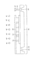
図4は、本発明の実施形態によるマルチフィンガートランジスタのレイアウトを説明するための平面図であり、図5ないし図8は、図4に示したマルチフィンガートランジスタをI−I、II−II、III−III、及びIV−IVに沿って見た断面図である。図面の簡単明瞭さのために、図4では第4配線の図示を省略し、図5ないし図8では各層の間に形成された層間絶縁膜の図示を省略した。 FIG. 4 is a plan view illustrating a layout of the multi-finger transistor according to the embodiment of the present invention. FIGS. 5 to 8 illustrate the multi-finger transistor illustrated in FIG. 4 as II, II-II, III. It is sectional drawing seen along -III and IV-IV. For the sake of simplicity of the drawing, the fourth wiring is not shown in FIG. 4, and the interlayer insulating film formed between the layers is omitted in FIGS.
図4及び図5ないし図8を参照すると、マルチフィンガートランジスタ400は、複数の単位セルを有し、前記単位セルはガードリング440によって定義される。図面では、一つの単位セルのみを示し、これからは一つの単位セルについてのみ説明する。
4 and 5 to 8, the
マルチフィンガートランジスタ400は、基板410内に第1アクティブ領域422及び第2アクティブ領域424を含むアクティブ領域420を有する。アクティブ領域420は、素子分離膜435によって定義されるフィールド領域430と区分される。素子分離膜435は酸化物を含むことができる。
The
基板410は、シリコンまたはゲルマニウムを含むことができる。基板410の上部にはP型またはN型不純物のドープされたP型またはN型ウェル(well)を形成することができる。本発明の一実施形態によると、基板410の上部にはP型ウェルが形成され、ガードリング440は、P+拡散領域であって前記P型ウェルにバイアス(bias)を提供する。
The
本発明の一実施形態によると、第1及び第2アクティブ領域(422、424)は実質的に同一の形状と面積を有する。これとは違って、第1及び第2アクティブ領域(422、424)は互いに異なる形状または面積を有することができる。特に、第1アクティブ領域422の幅である第1幅(W1)と第2アクティブ領域の幅である第2幅(W2)が互いに異なる値を有することができる。
According to an embodiment of the present invention, the first and second active regions (422, 424) have substantially the same shape and area. In contrast, the first and second
アクティブ領域420には、複数のゲートフィンガー452が形成される。本発明の一実施形態によると、各ゲートフィンガー452は、互いに平行でありかつ第1方向に延長するように形成する。
A plurality of
ゲートフィンガー452は、第1アクティブ領域422と第2アクティブ領域424との間に形成されたゲート接続部454によって互いに接続される。ゲート接続部454が第1アクティブ領域422と第2アクティブ領域424との間に形成されることによって、アクティブ領域とガードリングとの間にゲート接続部の形成された従来マルチフィンガーゲートに比べて、本発明の実施形態によるマルチフィンガーゲート400はゲート接続部454とガードリング440との距離を大きくすることができる。これによって、ゲート接続部454の上部に形成される第1配線480とガードリング440との距離(L1)も増加し、本発明の実施形態によるマルチフィンガーゲート400は低い寄生キャパシタンスを有することができる。
The
一方、本発明の一実施例によると、ゲート接続部454は、前記第1方向に実質的に垂直する第2方向に延長して形成される。
Meanwhile, according to an embodiment of the present invention, the
本発明の一実施形態によると、ゲートフィンガー452及びゲート接続部454は、ポリシリコンを含む。これとは違って、ゲートフィンガー452及びゲート接続部454は、金属を含むことができる。
According to an embodiment of the present invention, the
ゲートフィンガー452に隣接するアクティブ領域420には、ソース領域460及びドレイン領域470が形成される。具体的に、アクティブ領域420のゲートフィンガー452によってカバーされた部分間に複数のソース領域460及びドレイン領域470が交互に形成される。本発明の一実施形態によると、各ソース及びドレイン領域(460、470)は、前記第1方向に延長するように形成される。一方、基板410がP型ウェルを含む場合、ソース及びドレイン領域(460、470)はN型不純物のドープされたN+拡散領域になってもよい。
A
ゲート接続部454は、第1プラグ455を通じて第1配線480と電気的に接続される。第1ピラグ455は、導電性物質を含むことができる。
The
第1配線480は、第1プラグ455を通じてゲート接続部454と直接接続される第1接続部482及び第1接続部482から延長して外部信号の印加を受ける延長部484を含む。図示していないが、第1プラグ455は、第1層間絶縁膜を貫通するように形成することができ、第1配線480は、前記第1層間絶縁膜上に形成することができる。第1配線480は、金属のような導電性物質を含むことができる。
The
ガードリング440は、第4プラグ445を通じて第4配線447と電気的に接続される。第4プラグ445は導電性物質を含むことができる。
The
第4配線447は、接地線に接続することができ、金属のような導電性物質を含むことができる。また、第4プラグ445は、前記第1層間絶縁膜を貫通するように形成することができ、第4配線447は、前記第1層間絶縁膜上に形成することができる。
The
ソース領域460は、第2プラグ465を通じて第2配線490と電気的に接続される。第2プラグ465は導電性物質を含むことができる。
The
第2配線490は、第2プラグ465を通じて複数のソース領域460と直接接続される複数の第2接続部491及び第2接続部491とを互いに電気的に接続する第1接続部493を含む。第2配線490は、接地線に接続することができる。図示していないが、第2プラグ465は、前記第1層間絶縁膜及び前記第1層間絶縁膜上に形成された第2層間絶縁膜を貫通するように形成することができ、第2配線490は、前記第2層間絶縁膜上に形成することができる。第2配線490は、金属のような導電性物質を含むことができる。
The
第3配線495は、第3プラグ475を通じて複数のドレイン領域470と直接接続される複数の第3接続部497及び第3接続部497を互いに電気的に接続する第2接続部499を含む。第3配線495には入出力信号を印加することができる。本発明の一実施例によると、第3プラグ475は、前記第1及び第2層間絶縁膜を貫通するように形成することができ、第3配線495は、前記第2層間絶縁膜上に形成することができる。ここで、第2及び第3接続部(491、497)は前記第1方向に延長し、前記第2方向に交互に配置することができる。また、第1及び第2接続部(493、499)は前記第2方向に延長され、互いに対向するように配置することができる。
The
第3配線495は、金属のような導電性物質を含むことができる。本発明の一実施例よると、第2及び第3配線(490、495)は、同一の金属を含むことができ、第1配線480が含む金属と異なる金属を含むことができる。
The
図9は、比較例によるマルチトランジスタのレイアウトを説明するための平面図である。図9のマルチフィンガートランジスタ300は、従来の技術で言及したフォルデッドタイプトランジスタであって、図3に示したマルチフィンガートランジスタ300と同一である。ただし、本発明の実施例によるマルチフィンガートランジスタ400と比較するために、第1ないし第3配線を更に示した。
FIG. 9 is a plan view for explaining the layout of the multi-transistor according to the comparative example. The
図9を参照すると、アクティブ領域320の両側面にゲート接続部354が形成される。また、第1配線380が第1プラグ355を通じてゲート接続部354と電気的に接続されるようにゲート接続部354の上部に形成される。これによって、第1配線380とガードリング340との距離(L2)が図4に示したマルチフィンガートランジスタ400における第1配線480とガードリング440との距離(L1)よりも短い。よって、本発明の実施形態によるマルチフィンガートランジスタ400の寄生キャパシタンスが比較例によるマルチフィンガートランジスタ300の寄生キャパシタンスよりも小さくすることができ、これによって相対的に大きい値のカットオフ周波数を有することができる。
Referring to FIG. 9,
また、本発明の実施例によるマルチフィンガートランジスタ400は、比較例によるマルチフィンガートランジスタ300に比べて同一の単位セル面積で相対的に小さい寄生キャパシタンスを有するので、同一の寄生キャパシタンスを有すると仮定するとき、相対的に小さい単位セル面積を有することができる。
In addition, since the
一方、図9のマルチフィンガートランジスタ300において、第1配線380は第1プラグ355を通じてゲート接続部354と直接接続される第1接続部382、第1接続部382から延長して外部信号の印加を受ける延長部384及び第1接続部382と延長部384とを接続させるブリッジ部386を含む。ブリッジ部386が存在することによって、ブリッジ部386の長さだけゲート抵抗が増加するようになる。よって、本発明の実施例によるマルチフィンガートランジスタ400は、比較例によるマルチフィンガートランジスタ300に比べて低いゲート抵抗を有することができ、これによって相対的に大きい値の最大発振周波数を有することができる。
On the other hand, in the
以上、本発明の実施例によって詳細に説明したが、本発明はこれに限定されず、本発明が属する技術分野において通常の知識を有するものであれば本発明の思想と精神を離脱することなく、本発明を修正または変更できる。 As described above, the embodiments of the present invention have been described in detail. However, the present invention is not limited to these embodiments, and any person who has ordinary knowledge in the technical field to which the present invention belongs can be used without departing from the spirit and spirit of the present invention. The present invention can be modified or changed.
本発明によるマルチフィンガートランジスタでは、ガードリングに定義される単位セル内のアクティブ領域を二つに形成され、前記アクティブ領域の間にゲート接続部を形成する。これによって、前記ゲート接続部の上部に形成される配線と前記ガードリングとの距離が増加することによって、前記マルチフィンガートランジスタは小さい寄生キャパシタンスを有することができ、高いカットオフ周波数を有することができる。 In the multi-finger transistor according to the present invention, two active regions in the unit cell defined by the guard ring are formed, and a gate connection is formed between the active regions. As a result, the multi-finger transistor can have a small parasitic capacitance and a high cut-off frequency due to an increase in the distance between the wiring formed above the gate connection and the guard ring. .
また、前記配線が単位セルの中央部分に一つのみが配置されることによって、従来のフォルデッドタイプトランジスタに比べて小さいゲート抵抗を有することができ、高い最大発振周波数を有することができる。 In addition, since only one wiring is arranged at the central portion of the unit cell, it can have a smaller gate resistance than a conventional folded type transistor, and can have a high maximum oscillation frequency.
本発明は、マルチフィンガートランジスタの寄生キャパシタンスを小さくすることができ、ゲート抵抗を小さくすることができるため、高性能のマルチフィンガートランジスタの製造において使用することができる。 Since the parasitic capacitance of the multi-finger transistor can be reduced and the gate resistance can be reduced, the present invention can be used in the manufacture of a high-performance multi-finger transistor.
100 第1マルチフィンガートランジスタ、
110、210、310、410 基板、
120、220、320、420 アクティブ領域、
130、230、330、430 フィールド領域、
140、240、340、440 ガードリング、
145、245、345、445 第4プラグ、
150、250、350、450 マルチフィンガーゲート、
152、252、352、452 ゲートフィンガー、
154、254、354、454 ゲート接続部、
155、255、355、455 第1プラグ、
160、260、360、460 ソース領域、
170、270、370、470 ドレイン領域、
200 第2マルチフィンガートランジスタ、
300 第3マルチフィンガートランジスタ、
400 第4マルチフィンガートランジスタ、
447 第4配線、
465 第2プラグ、
475 第3プラグ、
480 第1配線、
490 第2配線、
495 第3配線、
100 first multi-finger transistor;
110, 210, 310, 410 substrate,
120, 220, 320, 420 active area,
130, 230, 330, 430 field region,
140, 240, 340, 440 guard ring,
145, 245, 345, 445 fourth plug,
150, 250, 350, 450 Multi-finger gate,
152, 252, 352, 452 gate fingers,
154, 254, 354, 454 gate connection,
155, 255, 355, 455 first plug,
160, 260, 360, 460 source region,
170, 270, 370, 470 drain region,
200 second multi-finger transistor,
300 third multi-finger transistor,
400 fourth multi-finger transistor,
447 Fourth wiring,
465 second plug,
475 Third plug,
480 1st wiring,
490 second wiring,
495 Third wiring,
Claims (14)
前記アクティブ領域内に形成された複数のゲートフィンガー、及び前記ゲートフィンガーを互いに接続して前記二つのアクティブ領域の間に形成されたゲート接続部を含むマルチフィンガーゲートと、
前記ゲートフィンガーに隣接する前記アクティブ領域の一部に形成された複数のソース領域と、
前記ゲートフィンガーに隣接する前記アクティブ領域の一部に形成された複数のドレイン領域と、を含むことを特徴とするマルチフィンガートランジスタ。 Two active areas defined in the unit cell of the substrate;
A multi-finger gate including a plurality of gate fingers formed in the active region, and a gate connection part formed between the two active regions by connecting the gate fingers to each other;
A plurality of source regions formed in a part of the active region adjacent to the gate finger;
And a plurality of drain regions formed in a part of the active region adjacent to the gate finger.
前記ソース領域と電気的に接続された第2配線と、
前記ドレイン領域と電気的に接続された第3配線と、を更に含むことを特徴とする請求項1に記載のマルチフィンガートランジスタ。 A first wiring electrically connected to the multi-finger gate;
A second wiring electrically connected to the source region;
The multi-finger transistor of claim 1, further comprising a third wiring electrically connected to the drain region.
Applications Claiming Priority (1)
| Application Number | Priority Date | Filing Date | Title |
|---|---|---|---|
| KR1020070019395A KR100873892B1 (en) | 2007-02-27 | 2007-02-27 | Multi-finger transistor |
Publications (2)
| Publication Number | Publication Date |
|---|---|
| JP2008211215A true JP2008211215A (en) | 2008-09-11 |
| JP2008211215A5 JP2008211215A5 (en) | 2011-03-31 |
Family
ID=39714883
Family Applications (1)
| Application Number | Title | Priority Date | Filing Date |
|---|---|---|---|
| JP2008041673A Pending JP2008211215A (en) | 2007-02-27 | 2008-02-22 | Multi-finger transistor |
Country Status (3)
| Country | Link |
|---|---|
| US (1) | US20080203444A1 (en) |
| JP (1) | JP2008211215A (en) |
| KR (1) | KR100873892B1 (en) |
Cited By (3)
| Publication number | Priority date | Publication date | Assignee | Title |
|---|---|---|---|---|
| JP2012134251A (en) * | 2010-12-20 | 2012-07-12 | Samsung Electro-Mechanics Co Ltd | High-frequency semiconductor switch |
| JP2016072532A (en) * | 2014-09-30 | 2016-05-09 | サンケン電気株式会社 | Semiconductor element |
| JP2016154182A (en) * | 2015-02-20 | 2016-08-25 | ローム株式会社 | Semiconductor device |
Families Citing this family (9)
| Publication number | Priority date | Publication date | Assignee | Title |
|---|---|---|---|---|
| CN102270659B (en) * | 2011-08-11 | 2012-09-26 | 中国科学院微电子研究所 | Multi-gate GaN high electron mobility transistors (HEMTs) |
| KR101299799B1 (en) * | 2011-10-24 | 2013-08-23 | 숭실대학교산학협력단 | Multi gate transistor |
| KR101977277B1 (en) * | 2012-10-29 | 2019-08-28 | 엘지이노텍 주식회사 | Power semiconductor device |
| US9269711B2 (en) * | 2013-07-01 | 2016-02-23 | Infineon Technologies Austria Ag | Semiconductor device |
| KR101666752B1 (en) | 2015-06-18 | 2016-10-14 | 주식회사 동부하이텍 | Semiconductor device and radio frequency module formed on high resistivity substrate |
| KR101666753B1 (en) | 2015-06-18 | 2016-10-14 | 주식회사 동부하이텍 | Semiconductor device and radio frequency module formed on high resistivity substrate |
| KR101692625B1 (en) | 2015-06-18 | 2017-01-03 | 주식회사 동부하이텍 | Semiconductor device and radio frequency module formed on high resistivity substrate |
| CN105742363B (en) * | 2016-03-21 | 2019-01-04 | 上海华虹宏力半导体制造有限公司 | RF switching devices and forming method thereof |
| CN111983411B (en) * | 2020-07-10 | 2022-12-27 | 中国电子科技集团公司第十三研究所 | Method and device for testing thermal resistance of multi-finger-gate transistor and terminal equipment |
Citations (6)
| Publication number | Priority date | Publication date | Assignee | Title |
|---|---|---|---|---|
| JP2004096118A (en) * | 2003-09-12 | 2004-03-25 | Hitachi Ltd | Semiconductor device and its manufacturing method |
| JP2004158813A (en) * | 2002-09-11 | 2004-06-03 | Toshiba Corp | Semiconductor device and manufacturing method therefor |
| JP2004335778A (en) * | 2003-05-08 | 2004-11-25 | Toshiba Corp | Semiconductor device |
| JP2005064462A (en) * | 2003-07-28 | 2005-03-10 | Nec Electronics Corp | Multi-finger type electrostatic discharging protective element |
| JP2005191031A (en) * | 2003-12-24 | 2005-07-14 | Renesas Technology Corp | Lateral direction diffusion type field effect semiconductor device |
| JP2005354014A (en) * | 2004-06-14 | 2005-12-22 | Nec Electronics Corp | Electrostatic discharge protection element |
Family Cites Families (5)
| Publication number | Priority date | Publication date | Assignee | Title |
|---|---|---|---|---|
| US4949139A (en) * | 1988-09-09 | 1990-08-14 | Atmel Corporation | Transistor construction for low noise output driver |
| US5789791A (en) | 1996-08-27 | 1998-08-04 | National Semiconductor Corporation | Multi-finger MOS transistor with reduced gate resistance |
| US6002156A (en) * | 1997-09-16 | 1999-12-14 | Winbond Electronics Corp. | Distributed MOSFET structure with enclosed gate for improved transistor size/layout area ratio and uniform ESD triggering |
| US7244975B2 (en) * | 2005-07-05 | 2007-07-17 | United Microelectronics Corp. | High-voltage device structure |
| US7689946B2 (en) * | 2006-10-19 | 2010-03-30 | International Business Machines Corporation | High-performance FET device layout |
-
2007
- 2007-02-27 KR KR1020070019395A patent/KR100873892B1/en not_active IP Right Cessation
-
2008
- 2008-02-20 US US12/071,339 patent/US20080203444A1/en not_active Abandoned
- 2008-02-22 JP JP2008041673A patent/JP2008211215A/en active Pending
Patent Citations (6)
| Publication number | Priority date | Publication date | Assignee | Title |
|---|---|---|---|---|
| JP2004158813A (en) * | 2002-09-11 | 2004-06-03 | Toshiba Corp | Semiconductor device and manufacturing method therefor |
| JP2004335778A (en) * | 2003-05-08 | 2004-11-25 | Toshiba Corp | Semiconductor device |
| JP2005064462A (en) * | 2003-07-28 | 2005-03-10 | Nec Electronics Corp | Multi-finger type electrostatic discharging protective element |
| JP2004096118A (en) * | 2003-09-12 | 2004-03-25 | Hitachi Ltd | Semiconductor device and its manufacturing method |
| JP2005191031A (en) * | 2003-12-24 | 2005-07-14 | Renesas Technology Corp | Lateral direction diffusion type field effect semiconductor device |
| JP2005354014A (en) * | 2004-06-14 | 2005-12-22 | Nec Electronics Corp | Electrostatic discharge protection element |
Cited By (3)
| Publication number | Priority date | Publication date | Assignee | Title |
|---|---|---|---|---|
| JP2012134251A (en) * | 2010-12-20 | 2012-07-12 | Samsung Electro-Mechanics Co Ltd | High-frequency semiconductor switch |
| JP2016072532A (en) * | 2014-09-30 | 2016-05-09 | サンケン電気株式会社 | Semiconductor element |
| JP2016154182A (en) * | 2015-02-20 | 2016-08-25 | ローム株式会社 | Semiconductor device |
Also Published As
| Publication number | Publication date |
|---|---|
| US20080203444A1 (en) | 2008-08-28 |
| KR100873892B1 (en) | 2008-12-15 |
| KR20080079377A (en) | 2008-09-01 |
Similar Documents
| Publication | Publication Date | Title |
|---|---|---|
| JP2008211215A (en) | Multi-finger transistor | |
| EP2368270B1 (en) | An improved rf cmos transistor design | |
| JP5086797B2 (en) | Semiconductor device | |
| US8035229B2 (en) | Semiconductor device | |
| US7777294B2 (en) | Semiconductor device including a high-breakdown voltage MOS transistor | |
| US20090242991A1 (en) | Semiconductor device | |
| US7999333B2 (en) | Semiconductor device | |
| JP6828588B2 (en) | Semiconductor device | |
| JP2018200916A (en) | Semiconductor device | |
| US9818833B2 (en) | Semiconductor device | |
| JP5586546B2 (en) | Semiconductor device | |
| US20210366902A1 (en) | Semiconductor integrated circuit device | |
| JP4215482B2 (en) | Electrostatic protection circuit and semiconductor device | |
| US11217604B2 (en) | Semiconductor device | |
| US8049279B2 (en) | Semiconductor device and method for fabricating the same | |
| US20190067185A1 (en) | Semiconductor Device and Layout Design Thereof | |
| JP2007019413A (en) | Semiconductor device for protection circuit | |
| JP2007027272A (en) | Semiconductor integrated circuit | |
| JP2004311824A (en) | Semiconductor integrated circuit | |
| US8710589B2 (en) | Semiconductor device | |
| JP2007273689A (en) | Semiconductor device | |
| US20200013901A1 (en) | Substrate contact for a transistor, intended in particular for a matrix-array arrangement | |
| US20100025816A1 (en) | Semiconductor device | |
| JP2008227197A (en) | Semiconductor device | |
| JPH09283752A (en) | Mis-type semiconductor device |
Legal Events
| Date | Code | Title | Description |
|---|---|---|---|
| A521 | Request for written amendment filed |
Free format text: JAPANESE INTERMEDIATE CODE: A523 Effective date: 20110210 |
|
| A621 | Written request for application examination |
Free format text: JAPANESE INTERMEDIATE CODE: A621 Effective date: 20110210 |
|
| A521 | Request for written amendment filed |
Free format text: JAPANESE INTERMEDIATE CODE: A523 Effective date: 20120113 |
|
| A977 | Report on retrieval |
Free format text: JAPANESE INTERMEDIATE CODE: A971007 Effective date: 20130228 |
|
| A131 | Notification of reasons for refusal |
Free format text: JAPANESE INTERMEDIATE CODE: A131 Effective date: 20130305 |
|
| A02 | Decision of refusal |
Free format text: JAPANESE INTERMEDIATE CODE: A02 Effective date: 20130730 |