JP2008166328A - Method of manufacturing conductive circuit board - Google Patents
Method of manufacturing conductive circuit board Download PDFInfo
- Publication number
- JP2008166328A JP2008166328A JP2006351003A JP2006351003A JP2008166328A JP 2008166328 A JP2008166328 A JP 2008166328A JP 2006351003 A JP2006351003 A JP 2006351003A JP 2006351003 A JP2006351003 A JP 2006351003A JP 2008166328 A JP2008166328 A JP 2008166328A
- Authority
- JP
- Japan
- Prior art keywords
- printed wiring
- solder
- wiring board
- solder powder
- conductive circuit
- Prior art date
- Legal status (The legal status is an assumption and is not a legal conclusion. Google has not performed a legal analysis and makes no representation as to the accuracy of the status listed.)
- Granted
Links
Classifications
-
- H—ELECTRICITY
- H05—ELECTRIC TECHNIQUES NOT OTHERWISE PROVIDED FOR
- H05K—PRINTED CIRCUITS; CASINGS OR CONSTRUCTIONAL DETAILS OF ELECTRIC APPARATUS; MANUFACTURE OF ASSEMBLAGES OF ELECTRICAL COMPONENTS
- H05K3/00—Apparatus or processes for manufacturing printed circuits
- H05K3/30—Assembling printed circuits with electric components, e.g. with resistors
- H05K3/32—Assembling printed circuits with electric components, e.g. with resistors electrically connecting electric components or wires to printed circuits
- H05K3/34—Assembling printed circuits with electric components, e.g. with resistors electrically connecting electric components or wires to printed circuits by soldering
- H05K3/3465—Application of solder
- H05K3/3485—Application of solder paste, slurry or powder
-
- H—ELECTRICITY
- H05—ELECTRIC TECHNIQUES NOT OTHERWISE PROVIDED FOR
- H05K—PRINTED CIRCUITS; CASINGS OR CONSTRUCTIONAL DETAILS OF ELECTRIC APPARATUS; MANUFACTURE OF ASSEMBLAGES OF ELECTRICAL COMPONENTS
- H05K3/00—Apparatus or processes for manufacturing printed circuits
- H05K3/30—Assembling printed circuits with electric components, e.g. with resistors
- H05K3/32—Assembling printed circuits with electric components, e.g. with resistors electrically connecting electric components or wires to printed circuits
- H05K3/34—Assembling printed circuits with electric components, e.g. with resistors electrically connecting electric components or wires to printed circuits by soldering
-
- H—ELECTRICITY
- H05—ELECTRIC TECHNIQUES NOT OTHERWISE PROVIDED FOR
- H05K—PRINTED CIRCUITS; CASINGS OR CONSTRUCTIONAL DETAILS OF ELECTRIC APPARATUS; MANUFACTURE OF ASSEMBLAGES OF ELECTRICAL COMPONENTS
- H05K2203/00—Indexing scheme relating to apparatus or processes for manufacturing printed circuits covered by H05K3/00
- H05K2203/04—Soldering or other types of metallurgic bonding
- H05K2203/0425—Solder powder or solder coated metal powder
-
- H—ELECTRICITY
- H05—ELECTRIC TECHNIQUES NOT OTHERWISE PROVIDED FOR
- H05K—PRINTED CIRCUITS; CASINGS OR CONSTRUCTIONAL DETAILS OF ELECTRIC APPARATUS; MANUFACTURE OF ASSEMBLAGES OF ELECTRICAL COMPONENTS
- H05K2203/00—Indexing scheme relating to apparatus or processes for manufacturing printed circuits covered by H05K3/00
- H05K2203/04—Soldering or other types of metallurgic bonding
- H05K2203/043—Reflowing of solder coated conductors, not during connection of components, e.g. reflowing solder paste
-
- H—ELECTRICITY
- H05—ELECTRIC TECHNIQUES NOT OTHERWISE PROVIDED FOR
- H05K—PRINTED CIRCUITS; CASINGS OR CONSTRUCTIONAL DETAILS OF ELECTRIC APPARATUS; MANUFACTURE OF ASSEMBLAGES OF ELECTRICAL COMPONENTS
- H05K2203/00—Indexing scheme relating to apparatus or processes for manufacturing printed circuits covered by H05K3/00
- H05K2203/12—Using specific substances
- H05K2203/122—Organic non-polymeric compounds, e.g. oil, wax or thiol
- H05K2203/124—Heterocyclic organic compounds, e.g. azole, furan
-
- H—ELECTRICITY
- H05—ELECTRIC TECHNIQUES NOT OTHERWISE PROVIDED FOR
- H05K—PRINTED CIRCUITS; CASINGS OR CONSTRUCTIONAL DETAILS OF ELECTRIC APPARATUS; MANUFACTURE OF ASSEMBLAGES OF ELECTRICAL COMPONENTS
- H05K3/00—Apparatus or processes for manufacturing printed circuits
- H05K3/22—Secondary treatment of printed circuits
- H05K3/28—Applying non-metallic protective coatings
- H05K3/282—Applying non-metallic protective coatings for inhibiting the corrosion of the circuit, e.g. for preserving the solderability
Landscapes
- Engineering & Computer Science (AREA)
- Manufacturing & Machinery (AREA)
- Microelectronics & Electronic Packaging (AREA)
- Electric Connection Of Electric Components To Printed Circuits (AREA)
Abstract
Description
本発明は、ハンダ回路基板の製造方法に関し、更に詳しくは、プリント配線板上の微細な導電性回路表面に、ハンダ層を形成する導電性回路基板の製造方法に関する。 The present invention relates to a method for manufacturing a solder circuit board, and more particularly to a method for manufacturing a conductive circuit board in which a solder layer is formed on a fine conductive circuit surface on a printed wiring board.
近年、プラスチック基板、セラミック基板、あるいはプラスチック等をコートした金属基板等の絶縁性基板上に、回路パターンを形成したプリント配線板が開発され、その回路パターン上にIC素子、半導体チップ、抵抗、コンデンサ等の電子部品をハンダ接合して電子回路を構成させる手段が広く採用されている。
この場合、電子部品のリード端子を、回路パターンの所定の部分に接合させるためには、基板上の導電性回路表面に予めハンダ薄層を形成させておき、ハンダペーストまたはフラックスを印刷し、所定の電子部品を位置決め載置した後、ハンダ薄層またはハンダ薄層及びハンダペーストをリフローさせ、ハンダ接続させるのが一般的である。
In recent years, a printed wiring board in which a circuit pattern is formed on an insulating substrate such as a plastic substrate, a ceramic substrate, or a metal substrate coated with plastic has been developed, and an IC element, a semiconductor chip, a resistor, a capacitor is formed on the circuit pattern. A means for soldering electronic components such as these to form an electronic circuit is widely used.
In this case, in order to join the lead terminal of the electronic component to a predetermined portion of the circuit pattern, a solder thin layer is formed in advance on the surface of the conductive circuit on the substrate, and solder paste or flux is printed, After the electronic components are positioned and mounted, the solder thin layer or the solder thin layer and the solder paste are generally reflowed and soldered.
また最近では電子製品の小型化のためハンダ回路基板にはファインピッチ化が要求され、ファインピッチの部品、例えば0.3mmピッチのQFP(Quad Flat Package)タイプのLSI、CSP(Chip Size Package)、0.15mmピッチのFC(Flip Chip)などが多く搭載されている。このため、ハンダ回路基板には、ファインピッチ対応の精細なハンダ回路パターンが要求されている。
プリント配線板にハンダ膜によるハンダ回路を形成するためには、メッキ法、HAL(ホットエアーレベラ)法、あるいはハンダ粉末のペーストを印刷しリフローする方法などが行われている。しかし、メッキ法によるハンダ回路の製造方法は、ハンダ層を厚くするのが困難であり、HAL法、ハンダペーストの印刷による方法は、ファインピッチパターンへの対応が困難である。
Recently, a fine pitch is required for a solder circuit board for miniaturization of electronic products. For example, a fine pitch component such as a 0.3 mm pitch QFP (Quad Flat Package) type LSI, a CSP (Chip Size Package), A large number of 0.15 mm pitch FC (Flip Chip) and the like are mounted. For this reason, a fine solder circuit pattern corresponding to the fine pitch is required for the solder circuit board.
In order to form a solder circuit using a solder film on a printed wiring board, a plating method, a HAL (hot air leveler) method, a method of printing a solder powder paste, and reflowing is performed. However, it is difficult for the solder circuit manufacturing method by the plating method to increase the thickness of the solder layer, and the HAL method and the solder paste printing method are difficult to cope with the fine pitch pattern.
そのため、回路パターンの位置合わせ等の面倒な操作を必要とせずハンダ回路を形成する方法として、プリント配線板の導電性回路表面に、粘着性付与化合物を反応させることにより粘着性を付与し、該粘着部にハンダ粉末を付着させ、次いで該プリント配線板を加熱し、ハンダを溶解してハンダ回路を形成する方法が開示されている(例えば、特許文献1参照。)。
また、特許文献1で開示されたプリント配線板へのハンダ粉末の付着方法は乾式で行うが、ハンダ粉末が静電気により余分な部分に付着したり、ハンダ粉末の飛散等が生ずる場合があるため、プリント配線板を、ハンダ粉末を含むスラリー中に浸漬することにより、粘着性を付与した回路部分にハンダ粉末を湿式プロセスで付着させる方法が開示されている(例えば、特許文献2参照。)。
In addition, the method of attaching solder powder to the printed wiring board disclosed in Patent Document 1 is performed by a dry method, but solder powder may adhere to an excess part due to static electricity or solder powder may be scattered. A method is disclosed in which a printed wiring board is immersed in a slurry containing solder powder so that the solder powder adheres to a circuit portion to which tackiness has been imparted by a wet process (see, for example, Patent Document 2).
特許文献1に記載された方法は、プリント配線板の回路部分の金属と、ナフトトリアゾール系誘導体等の物質とを反応させ、その金属部分に金属錯体を形成し、その金属錯体の粘着性を利用してハンダ粉末を付着させる。この金属錯体の粘着力は、時間の経過と共に低下するため、プリント配線板の回路部分に粘着性を付与した後は、速やかに、その粘着部分にハンダ粉末を付着させる必要があった。そのため、プリント配線板の回路部分に粘着性を付与する工程と、その粘着部分にハンダ粉末を付着させる工程は、その工程のスループットをあわせる必要があった。そして、装置トラブル等の理由により、ハンダ粉末を付着させる工程のスループットが低下した場合は、粘着性を付与した基板が滞留し、その基板の粘着性が低下する場合があった。このような場合、そのプリント配線板は、再度、その回路部分に粘着性を発現させる必要があった。 The method described in Patent Document 1 reacts a metal of a circuit part of a printed wiring board with a substance such as a naphthotriazole derivative to form a metal complex in the metal part, and utilizes the adhesiveness of the metal complex. Then, solder powder is attached. Since the adhesive strength of this metal complex decreases with the passage of time, it was necessary to quickly attach solder powder to the adhesive portion after imparting adhesiveness to the circuit portion of the printed wiring board. Therefore, it is necessary to match the throughput of the process of imparting adhesiveness to the circuit part of the printed wiring board and the process of attaching solder powder to the adhesive part. And when the throughput of the process which makes solder powder adhere falls for reasons, such as an apparatus trouble, the board | substrate which gave adhesiveness stagnates and the adhesiveness of the board | substrate may fall. In such a case, the printed wiring board needs to express adhesiveness in the circuit portion again.
本発明はこの問題点を解決し、プリント配線板の回路部分に付与した粘着性を持続させることにより、プリント配線板の回路部分に粘着性を付与する工程と、その粘着部分にハンダ粉末を付着させる工程との間の、プリント配線板の処理待可能な時間を長くし、円滑に導電性回路基板を製造することを可能とする方法を提供することを目的とする。 The present invention solves this problem and maintains the adhesiveness imparted to the circuit portion of the printed wiring board, thereby attaching the adhesiveness to the circuit portion of the printed wiring board, and adheres solder powder to the adhesive portion. It is an object of the present invention to provide a method that makes it possible to prolong a time during which a printed wiring board can be processed during the process of making the conductive circuit board and to smoothly manufacture a conductive circuit board.
本発明者は、上記課題を解決すべく鋭意努力検討した結果、本発明に到達した。即ち本発明は、以下に関する。
(1)プリント配線板上の導電性回路表面に粘着性付与化合物を用いて粘着性を付与し、該粘着部にハンダ粉末を付着させ、次いで該プリント配線板を加熱し、ハンダを溶融してハンダ回路を形成する導電性回路基板の製造方法であって、粘着性を付与した後でハンダ粉末を付着させる前のプリント配線板を、10℃以下で保存することを特徴とする導電性回路基板の製造方法。
(2)プリント配線板上の導電性回路表面に粘着性付与化合物を用いて粘着性を付与し、該粘着部にハンダ粉末を付着させ、次いで該プリント配線板を加熱し、ハンダを溶融してハンダ回路を形成する導電性回路基板の製造方法であって、粘着性を付与した後でハンダ粉末を付着させる前のプリント配線板を、10℃以下の液中に保存することを特徴とする導電性回路基板の製造方法。
(3)粘着性付与化合物が、ナフトトリアゾール系誘導体、べンゾトリアゾール系誘導体、イミダゾール系誘導体、べンゾイミダゾール系誘導体、メルカプトべンゾチアゾール系誘導体、べンゾチアゾールチオ脂肪酸からなる群から選ばれた何れか一種以上の物質を含むことを特徴とする上記(1)または(2)に記載の導電性回路基板の製造方法。
The inventor of the present invention has reached the present invention as a result of diligent efforts to solve the above problems. That is, the present invention relates to the following.
(1) Adhesion is imparted to the surface of the conductive circuit on the printed wiring board using a tackifier compound, solder powder is adhered to the adhesive part, and then the printed wiring board is heated to melt the solder. A method of manufacturing a conductive circuit board for forming a solder circuit, wherein the printed circuit board is coated at 10 ° C. or lower after the adhesive powder is applied and before the solder powder is applied. Manufacturing method.
(2) Adhesiveness is imparted to the surface of the conductive circuit on the printed wiring board using a tackifier compound, solder powder is adhered to the adhesive part, and then the printed wiring board is heated to melt the solder. A method for producing a conductive circuit board for forming a solder circuit, characterized in that a printed wiring board after adhesion is applied and before solder powder is deposited is stored in a liquid at 10 ° C. or lower. Method for manufacturing a circuit board.
(3) The tackifier compound is selected from the group consisting of naphthotriazole derivatives, benzotriazole derivatives, imidazole derivatives, benzoimidazole derivatives, mercaptobenzothioazole derivatives, and benzothiazole thio fatty acids. The method for producing a conductive circuit board according to the above (1) or (2), comprising any one or more substances.
(4)プリント配線板を保存する液中の保存温度が10℃以下、液体の凍結温度以上である上記(2)又は(3)に記載の導電性回路基板の製造方法。
(5)プリント配線板を保存する液体が水であることを特徴とする上記(2)〜(4)のいずれか1項に記載の導電性回路基板の製造方法。
(6)プリント配線板にハンダ粉末を付着させる工程を、ハンダ粉末を含む液体中で行うことを特徴とする上記(2)〜(5)の何れか1項に記載の導電性回路基板の製造方法。
(7)液体が水である上記(6)に記載の導電性回路基板の製造方法。
(8)液体中のハンダ粉末の濃度が0.5〜10体積%である上記(6)又は(7)に記載の導電性回路基板の製造方法。
(9)プリント配線板にハンダ粉末を付着させる際の、ハンダ粉末を含む液体の液温度が、30℃〜45℃の範囲内であることを特徴とする上記(6)〜(8)の何れか1項に記載の導電性回路基板の製造方法。
(4) The method for producing a conductive circuit board according to the above (2) or (3), wherein the storage temperature in the liquid for storing the printed wiring board is 10 ° C. or lower and the liquid freezing temperature or higher.
(5) The method for producing a conductive circuit board according to any one of (2) to (4), wherein the liquid for storing the printed wiring board is water.
(6) The process for adhering solder powder to a printed wiring board is performed in a liquid containing solder powder, wherein the conductive circuit board according to any one of (2) to (5) is manufactured. Method.
(7) The method for producing a conductive circuit board according to (6), wherein the liquid is water.
(8) The method for producing a conductive circuit board according to (6) or (7), wherein the concentration of the solder powder in the liquid is 0.5 to 10% by volume.
(9) Any of the above (6) to (8), wherein the temperature of the liquid containing the solder powder is within the range of 30 ° C. to 45 ° C. when the solder powder is adhered to the printed wiring board. A method for producing a conductive circuit board according to claim 1.
本発明は、微細な回路パターンや微少なバンプを有するプリント配線板の製造工程において、工程間の処理待可能な時間を長くすることを可能とするため、装置トラブル等による再処理等の工程を減らし、プリント配線板の製造における生産性を高めることを可能とする。 In the manufacturing process of a printed wiring board having a minute circuit pattern and a minute bump, the present invention makes it possible to lengthen the waiting time between the processes, so that a process such as reprocessing due to an apparatus trouble or the like is performed. This makes it possible to increase productivity in the production of printed wiring boards.
本発明を、その製造プロセスの順に、詳細に説明する。
本発明の対象となるプリント配線板は、プラスチック基板、プラスチックフィルム基板、ガラス布基板、紙基質エポキシ樹脂基板、セラミックス基板等に金属板を積層した基板、あるいは金属基材にプラスチックあるいはセラミックス等を被覆した絶縁基板上に、金属等の導電性物質を用いて回路パターンを形成した片面プリント配線板、両面プリント配線板、多層プリント配線板あるいはフレキシブルプリント配線板等である。その他、IC基板、コンデンサ、抵抗、コイル、バリスタ、ベアチップ、ウェーハ等への適用も可能である。
この中で、本発明は、BGA(ボール・グリッド・アレイ)やCSP(チップ・サイズ・パッケージ)接合用等のバンプ形成に適用するのが好ましい。
The present invention will be described in detail in the order of its manufacturing process.
The printed wiring board that is the subject of the present invention is a plastic substrate, a plastic film substrate, a glass cloth substrate, a paper substrate epoxy resin substrate, a substrate in which a metal plate is laminated on a ceramic substrate, or a metal substrate coated with plastic or ceramics. A single-sided printed wiring board, a double-sided printed wiring board, a multilayer printed wiring board, a flexible printed wiring board, or the like in which a circuit pattern is formed on a conductive substrate such as metal on the insulating substrate. In addition, application to IC substrates, capacitors, resistors, coils, varistors, bare chips, wafers, and the like is also possible.
Of these, the present invention is preferably applied to bump formation for bonding a BGA (ball grid array) or CSP (chip size package).
本発明は、上記プリント配線板上の導電性回路表面を、粘着性付与化合物と反応させることにより粘着性を付与し、該粘着部にハンダ粉末を付着させ、次いで該プリント配線板を加熱し、ハンダを溶融して回路基板にハンダ層を先ず形成する。
回路を形成する導電性物質としては、ほとんどの場合銅が用いられているが、本発明ではこれに限定されず、後述する粘着性付与物質により表面に粘着性が得られる導電性の物質であればよい。これらの物質として、例えば、Ni、Sn、Ni−Au、ハンダ合金等を含む物質が例示できる。
In the present invention, the surface of the conductive circuit on the printed wiring board is reacted with a tackifier compound to impart tackiness, and solder powder is attached to the adhesive portion, and then the printed wiring board is heated, First, a solder layer is formed on the circuit board by melting the solder.
In most cases, copper is used as a conductive material for forming a circuit. However, the present invention is not limited to this, and any conductive material can be used that provides adhesion to the surface by a tackifier that will be described later. That's fine. Examples of these substances include substances containing Ni, Sn, Ni—Au, solder alloys, and the like.
本発明で用いる粘着性付与化合物は、ナフトトリアゾール系誘導体、べンゾトリアゾール系誘導体、イミダゾール系誘導体、べンゾイミダゾール系誘導体、メルカプトべンゾチアゾール系誘導体及びべンゾチアゾールチオ脂肪酸からなる群から選ばれる何れか一種以上を含む物質を用いるのが好ましい。これらの粘着性付与化合物は特に銅に対しての効果が強いが、他の導電性物質にも粘着性を付与することができる。 The tackifier compound used in the present invention is selected from the group consisting of naphthotriazole derivatives, benzotriazole derivatives, imidazole derivatives, benzoimidazole derivatives, mercaptobenzobenzothiazole derivatives, and benzothiazole thio fatty acids. It is preferable to use a substance containing any one or more of the above. These tackifying compounds have a particularly strong effect on copper, but can also provide tackiness to other conductive substances.
本発明においては、べンゾトリアゾール系誘導体は一般式(1)で表される。
(但し、R1〜R4は、独立に水素原子、炭素数が1〜16、好ましくは、5〜16のアルキル基、アルコキシ基、F、Br、Cl、I、シアノ基、アミノ基またはOH基を表す。)
In the present invention, the benzotriazole derivative is represented by the general formula (1).
(However, R1 to R4 independently represent a hydrogen atom, an alkyl group having 1 to 16, preferably 5 to 16 carbon atoms, an alkoxy group, F, Br, Cl, I, a cyano group, an amino group, or an OH group. To express.)
ナフトトリアゾール系誘導体は一般式(2)で表される。
(但し、R5〜R10は、独立に水素原子、炭素数が1〜16、好ましくは、5〜16のアルキル基、アルコキシ基、F、Br、Cl、I、シアノ基、アミノ基またはOH基を表す。)
The naphthotriazole derivative is represented by the general formula (2).
(However, R5 to R10 independently represent a hydrogen atom, an alkyl group having 1 to 16, preferably 5 to 16 carbon atoms, an alkoxy group, F, Br, Cl, I, a cyano group, an amino group, or an OH group. To express.)
イミダゾール系誘導体は一般式(3)で表される。
(但し、R11、R12は、独立に水素原子、炭素数が1〜16、好ましくは、5〜16のアルキル基、アルコキシ基、F、Br、Cl、I、シアノ基、アミノ基またはOH基を表す。)
The imidazole derivative is represented by the general formula (3).
(However, R11 and R12 independently represent a hydrogen atom, an alkyl group having 1 to 16, preferably 5 to 16 carbon atoms, an alkoxy group, F, Br, Cl, I, a cyano group, an amino group, or an OH group. To express.)
べンゾイミダゾール系誘導体は一般式(4)で表される。
(但し、R13〜R17は、独立に水素原子、炭素数が1〜16、好ましくは、5〜16のアルキル基、アルコキシ基、F、Br、Cl、I、シアノ基、アミノ基またはOH基を表す。)
The benzimidazole derivative is represented by the general formula (4).
(However, R13 to R17 each independently represents a hydrogen atom, an alkyl group having 1 to 16, preferably 5 to 16 carbon atoms, an alkoxy group, F, Br, Cl, I, a cyano group, an amino group, or an OH group. To express.)
メルカプトべンゾチアゾール系誘導体は一般式(5)で表される。
(R18〜R21は、独立に水素原子、炭素数が1〜16、好ましくは、5〜16のアルキル基、アルコキシ基、F、Br、Cl、I、シアノ基、アミノ基またはOH基を表す。)
Mercaptobenzothiazole derivatives are represented by general formula (5).
(R18 to R21 independently represent a hydrogen atom, an alkyl group having 1 to 16, preferably 5 to 16 carbon atoms, an alkoxy group, F, Br, Cl, I, a cyano group, an amino group, or an OH group. )
べンゾチアゾールチオ脂肪酸系誘導体は一般式(6)で表される。
(但し、R22〜R26は、独立に水素原子、炭素数が1〜16、好ましくは、1または2のアルキル基、アルコキシ基、F、Br、Cl、I、シアノ基、アミノ基またはOH基を表す。)
The benzothiazole thio fatty acid derivative is represented by the general formula (6).
(However, R22 to R26 independently represent a hydrogen atom, an alkyl group having 1 to 16, preferably 1 or 2, an alkyl group, an alkoxy group, F, Br, Cl, I, a cyano group, an amino group, or an OH group. To express.)
これらの化合物のうち、一般式(1)で示されるべンゾトリアゾール系誘導体としてはR1〜R4は、一般には炭素数が多いほうが粘着性が強い。
一般式(3)及び一般式(4)で示されるイミダゾール系誘導体及びべンゾイミダゾール系誘導体のR11〜R17においても、一般に炭素数の多いほうが粘着性が強い。
一般式(6)で示されるべンゾチアゾールチオ脂肪酸系誘導体においては、R22〜R26は炭素数1または2が好ましい。
Among these compounds, as the benzotriazole derivatives represented by the general formula (1), R1 to R4 generally have higher adhesion as the number of carbon atoms increases.
Also in R11 to R17 of the imidazole derivatives and benzoimidazole derivatives represented by the general formula (3) and the general formula (4), in general, the higher the number of carbon atoms, the stronger the adhesiveness.
In the benzothiazole thio fatty acid derivative represented by the general formula (6), R22 to R26 preferably have 1 or 2 carbon atoms.
本発明では、該粘着性付与化合物の少なくとも一つを水または酸性水に溶解し、好ましくはpH3〜4程度の微酸性に調整して用いる。pHの調整に用いる物質としては、導電性物質が金属であるときは塩酸、硫酸、硝酸、リン酸等の無機酸をあげることができる。また有機酸としては、蟻酸、酢酸、プロピオン酸、リンゴ酸、シュウ酸、マロン酸、コハク酸、酒石酸等が使用できる。該粘着性付与化合物の濃度は厳しく限定はされないが溶解性、使用状況に応じて適宜調整して用いるが、好ましくは全体として0.05質量%〜20質量%の範囲内の濃度が使用しやすい。これより低濃度にすると粘着性膜の生成が不十分となり、性能上好ましくない。 In the present invention, at least one of the tackifying compounds is dissolved in water or acidic water, and adjusted to slightly acidic, preferably about pH 3-4. Examples of the substance used for adjusting the pH include inorganic acids such as hydrochloric acid, sulfuric acid, nitric acid, and phosphoric acid when the conductive substance is a metal. As the organic acid, formic acid, acetic acid, propionic acid, malic acid, oxalic acid, malonic acid, succinic acid, tartaric acid and the like can be used. The concentration of the tackifier compound is not strictly limited, but is appropriately adjusted according to solubility and use conditions, but preferably a concentration in the range of 0.05% by mass to 20% by mass is easy to use as a whole. . If the concentration is lower than this, the formation of an adhesive film becomes insufficient, which is not preferable in terms of performance.
処理温度は室温よりは若干加温したほうが粘着性膜の生成速度、生成量が良い。粘着性付与化合物濃度、金属の種類などにより変わり限定的でないが、一般的には30℃〜60℃位の範囲が好適である。浸漬時間は限定的でないが、作業効率から5秒〜5分間位の範囲になるように他の条件を調整することが好ましい。
なおこの場合、溶液中に銅をイオンとして100〜1000ppmを共存させると、粘着性膜の生成速度、生成量などの生成効率が高まるので好ましい。
The treatment temperature and the production amount of the adhesive film are better when the treatment temperature is slightly warmer than room temperature. Although it varies depending on the tackifying compound concentration, the type of metal, and the like, it is generally in the range of about 30 ° C to 60 ° C. Although immersion time is not limited, it is preferable to adjust other conditions so that it may become the range of 5 second-about 5 minutes from work efficiency.
In this case, it is preferable to coexist 100 to 1000 ppm with copper as ions in the solution because the production efficiency such as the production rate and production amount of the adhesive film is increased.
処理すべきプリント配線板は、ハンダ層の形成が不要の導電性回路部分をレジスト等で覆い、ハンダ層の形成が必要な回路パターンの部分のみが露出した状態にしておき、粘着性付与化合物溶液で処理するのが好ましい。
また、本願発明の導電性回路基板の製造方法は、プリント配線板上に形成した例えば円状の微小な電極部分に、ハンダボールを1個だけ付着させる、いわゆる単粒子付着に用いることが好ましい。プリント配線板を単粒子付着により製造する場合は、各電極部分に1個のハンダボールのみを付着させるため、その箇所にハンダボールが付着しなかった場合は、そのプリント配線板は不良品となってしまう。よって、導電性回路表面の粘着力は高度に管理する必要があり、本願発明の製造方法を用いるのに適している。
ここで使用する前述の粘着性付与化合物溶液にプリント配線板を浸漬するか、または溶液を塗布すると、導電性回路表面が粘着性を示す。
For the printed wiring board to be processed, the conductive circuit portion that does not require the formation of a solder layer is covered with a resist or the like, and only the portion of the circuit pattern that requires the formation of a solder layer is exposed. It is preferable to treat with.
The method for producing a conductive circuit board of the present invention is preferably used for so-called single particle adhesion, in which only one solder ball is adhered to, for example, a circular minute electrode portion formed on a printed wiring board. When a printed wiring board is manufactured by adhering single particles, only one solder ball is attached to each electrode portion. If the solder ball does not adhere to that portion, the printed wiring board becomes a defective product. End up. Therefore, it is necessary to manage the adhesive strength of the conductive circuit surface to a high degree, and it is suitable for using the manufacturing method of the present invention.
When the printed wiring board is immersed in the above-mentioned tackifier compound solution used here or the solution is applied, the surface of the conductive circuit exhibits tackiness.
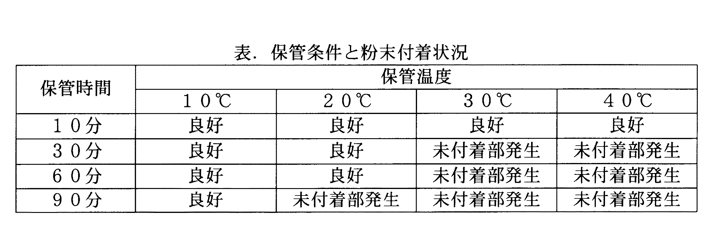
以上の方法で、導電性回路表面に付与された粘着性は、例えば40℃では、10分間程度しか、ハンダ粉末を十分に付着させるための粘着力が保持されない。すなわち、本願発明の導電性回路基板の製造方法を用いない場合は、この粘着性が保持される時間以内に、次工程である、導電性回路表面の粘着部分へのハンダ粉末の付着工程を行う必要があった。
本願発明では、導電性回路表面に付与された粘着性を、より長い時間持続させるために、粘着性を付与した後でハンダ粉末を付着させる前のプリント配線板を、10℃以下にして保存することを特徴とする。保存は大気中、あるいは窒素雰囲気などの気体中でも可能であるが、液体中が好ましい。このような条件下に粘着性を付与したプリント配線板を保持すると、その粘着力を2時間程度まで維持することが可能となる。すなわち、従来の製造方法では、粘着性を付与したプリント配線板は、10分間程度以内に次工程の、導電性回路表面の粘着部分へのハンダ粉末の付着工程を行う必要があったが、本発明の製造方法を用いた場合は、その処理待ち時間を2時間程度まで拡張できるため、粘着性付与工程、および、ハンダ粉末の付着工程において、より自由度の高い製造条件を設定することが可能となった。さらに、粘着性が低下したプリント配線板を再処理して粘着性を高めるなどの無駄な工程を低減させることが可能となった。
With the above method, the adhesiveness imparted to the surface of the conductive circuit is such that, for example, at 40 ° C., the adhesive force for sufficiently attaching the solder powder is maintained only for about 10 minutes. That is, when the manufacturing method of the conductive circuit board of the present invention is not used, the solder powder is adhered to the adhesive portion of the surface of the conductive circuit, which is the next step, within the time during which the adhesiveness is maintained. There was a need.
In the present invention, in order to maintain the adhesiveness applied to the surface of the conductive circuit for a longer period of time, the printed wiring board after applying the adhesive and before attaching the solder powder is stored at 10 ° C. or lower. It is characterized by that. Storage can be performed in the air or in a gas such as a nitrogen atmosphere, but is preferably in a liquid. Holding a printed wiring board to which tackiness has been imparted under such conditions makes it possible to maintain the adhesive strength for up to about 2 hours. That is, according to the conventional manufacturing method, the printed wiring board to which the adhesiveness has been imparted needs to be subjected to the solder powder adhesion step on the adhesive portion of the conductive circuit surface within about 10 minutes. When the manufacturing method of the invention is used, the processing waiting time can be extended to about 2 hours, so it is possible to set manufacturing conditions with a higher degree of freedom in the tackifying step and the solder powder attaching step. It became. Furthermore, it has become possible to reduce useless processes such as reprocessing a printed wiring board having reduced adhesiveness to increase adhesiveness.
10℃以下だと何故粘着性が下がらないのか、その理由の詳細は不明であるが、粘着性がなくなる理由が表面の改質、粘着付与物質の溶解等であることを鑑みれば、粘着物の化学反応性の低下や、溶解性(液体中の保存の場合)の低下が考えられる。
本願発明では、導電性回路表面に付与された粘着性を、より長い時間持続させるために、粘着性を付与した後でハンダ粉末を付着させる前のプリント配線板を、10℃以下で保存するが、その下限の温度は気体の場合は、粘着物の凍結温度、液体の場合は0℃、または、その液および粘着物の凍結温度である。必要以上に液温度を下げても、それほどの粘着性の持続効果は得られず、また、液体の場合、液が凍結しやすくなるなど液温度の管理が難しくなるからである。本願発明では、プリント配線板を液体中で保存する場合、液体としては水が好ましい。
水が好ましい理由は粘着物に影響を与えにくいためであり、また、粘着物の粘着発生機構に水が関与しているからである。
The reason why the adhesiveness does not decrease when it is 10 ° C. or lower is unknown, but considering that the reasons for the absence of adhesiveness are surface modification, dissolution of the tackifier, etc. A decrease in chemical reactivity and a decrease in solubility (when stored in a liquid) can be considered.
In the present invention, in order to maintain the adhesiveness imparted to the surface of the conductive circuit for a longer time, the printed wiring board after the adhesiveness is applied and before the solder powder is adhered is stored at 10 ° C. or lower. The lower limit temperature is the freezing temperature of the sticky substance in the case of gas, 0 ° C. in the case of liquid, or the freezing temperature of the liquid and sticky substance. This is because even if the liquid temperature is lowered more than necessary, such a sticky sustaining effect cannot be obtained, and in the case of a liquid, it becomes difficult to manage the liquid temperature because the liquid is easily frozen. In the present invention, when the printed wiring board is stored in a liquid, water is preferable as the liquid.
The reason why water is preferable is that it is difficult to affect the sticky material, and that water is involved in the sticking generation mechanism of the sticky material.
本発明では粘着性付与化合物として、ナフトトリアゾール系誘導体、べンゾトリアゾール系誘導体、イミダゾール系誘導体、べンゾイミダゾール系誘導体、メルカプトべンゾチアゾール系誘導体、べンゾチアゾールチオ脂肪酸等を用いるのが好ましいが、これらの物質により形成された金属錯体の粘着力を保持するためには水が最も好ましいからである。
本願発明では、プリント配線板の粘着部分にハンダ粉末を付着させる工程を、ハンダ粉末を含む液体中で行い、またその際の、ハンダ粉末を含む液体の液温度を、30℃〜45℃の範囲内とするのが好ましい。プリント配線板の粘着部分にハンダ粉末を付着させる工程を湿式で行うことにより、ハンダ粉末が静電気により余分な部分に付着すること、また、粉末が飛散等することを防止できる。また、ハンダ粉末を含む液体の液温度を、30℃〜45℃の範囲内とすることにより、粘着部分におけるハンダ粉末の付着力を最も高めることが可能となる。
In the present invention, it is preferable to use a naphthotriazole derivative, a benzotriazole derivative, an imidazole derivative, a benzoimidazole derivative, a mercaptobenzothioazole derivative, a benzothiazole thio fatty acid, etc. as the tackifier compound. However, water is most preferable in order to maintain the adhesive strength of the metal complex formed by these substances.
In this invention, the process which makes solder powder adhere to the adhesion part of a printed wiring board is performed in the liquid containing solder powder, and the liquid temperature of the liquid containing solder powder in that case is the range of 30 to 45 degreeC. It is preferable to be inside. By performing the process of adhering the solder powder to the adhesive part of the printed wiring board in a wet manner, it is possible to prevent the solder powder from adhering to an excess part due to static electricity and the scattering of the powder. Moreover, by making the liquid temperature of the liquid containing the solder powder within the range of 30 ° C. to 45 ° C., it becomes possible to maximize the adhesion of the solder powder in the adhesive portion.
ハンダ粉末の付着を液体中で行なうには具体的には、はんだ粉末を含むスラリーを入れた容器に、基板を水平に浸漬させ、さらに、はんだ粉末を含むスラリーをポンプで循環させて、その吐出ノズルを基板の電極部直上に設ける。また、基板を超音波振動させても良い。
本発明に用いるハンダ粉末を含む液体は、液体中のハンダ粉末の濃度を、好ましくは0.5体積%〜10体積%の範囲内、より好ましくは、3体積%〜8体積%の範囲内とする。
本発明に用いるハンダ粉末を含む液体は、その溶媒として、水を用いるのが好ましい。また水によりハンダ粉末が酸化するのを防ぐため、脱酸素した水を用ること、また、水に防錆剤を添加することが好ましい。
In order to adhere the solder powder in the liquid, specifically, the substrate is immersed horizontally in a container containing the slurry containing the solder powder, and the slurry containing the solder powder is circulated by a pump and discharged. A nozzle is provided immediately above the electrode portion of the substrate. Further, the substrate may be ultrasonically vibrated.
The liquid containing the solder powder used in the present invention preferably has a concentration of the solder powder in the liquid in the range of 0.5 vol% to 10 vol%, more preferably in the range of 3 vol% to 8 vol%. To do.
The liquid containing the solder powder used in the present invention preferably uses water as the solvent. Further, in order to prevent the solder powder from being oxidized by water, it is preferable to use deoxygenated water and to add a rust inhibitor to the water.
本発明のハンダ回路基板の製造方法に使用するハンダ粉末の金属組成としては、例えばSn−Pb系、Sn−Pb−Ag系、Sn−Pb−Bi系、Sn−Pb−Bi−Ag系、Sn−Pb−Cd系が挙げられる。また最近の産業廃棄物におけるPb排除の観点から、Pbを含まないSn−In系、Sn−Bi系、In−Ag系、In−Bi系、Sn−Zn系、Sn−Ag系、Sn−Cu系、Sn−Sb系、Sn−Au系、Sn−Bi−Ag−Cu系、Sn−Ge系、Sn−Bi−Cu系、Sn−Cu−Sb−Ag系、Sn−Ag−Zn系、Sn−Cu−Ag系、Sn−Bi−Sb系、Sn−Bi−Sb−Zn系、Sn−Bi−Cu−Zn系、Sn−Ag−Sb系、Sn−Ag−Sb−Zn系、Sn−Ag−Cu−Zn系、Sn−Zn−Bi系が好ましい。 Examples of the metal composition of the solder powder used in the method for manufacturing a solder circuit board of the present invention include Sn-Pb, Sn-Pb-Ag, Sn-Pb-Bi, Sn-Pb-Bi-Ag, and Sn. -Pb-Cd system is mentioned. Further, from the viewpoint of eliminating Pb in recent industrial waste, Sn-In, Sn-Bi, In-Ag, In-Bi, Sn-Zn, Sn-Ag, Sn-Cu, which does not contain Pb. -Based, Sn-Sb-based, Sn-Au-based, Sn-Bi-Ag-Cu-based, Sn-Ge-based, Sn-Bi-Cu-based, Sn-Cu-Sb-Ag-based, Sn-Ag-Zn-based, Sn -Cu-Ag system, Sn-Bi-Sb system, Sn-Bi-Sb-Zn system, Sn-Bi-Cu-Zn system, Sn-Ag-Sb system, Sn-Ag-Sb-Zn system, Sn-Ag -Cu-Zn type and Sn-Zn-Bi type are preferable.
上記の具体例としては、Snが63質量%、Pbが37質量%の共晶ハンダ(以下63Sn−37Pbと表す。)を中心として、62Sn−36Pb−2Ag、62.6Sn−37Pb−0.4Ag、60Sn−40Pb、50Sn−50Pb、30Sn−70Pb、25Sn−75Pb、10Sn−88Pb−2Ag、46Sn−8Bi−46Pb、57Sn−3Bi−40Pb、42Sn−42Pb−14Bi−2Ag、45Sn−40Pb−15Bi、50Sn−32Pb−18Cd、48Sn−52In、43Sn−57Bi、97In−3Ag、58Sn−42In、95In−5Bi、60Sn−40Bi、91Sn−9Zn、96.5Sn−3.5Ag、99.3Sn−0.7Cu、95Sn−5Sb、20Sn−80Au、90Sn−10Ag、90Sn−7.5Bi−2Ag−0.5Cu、97Sn−3Cu、99Sn−1Ge、92Sn−7.5Bi−0.5Cu、97Sn−2Cu−0.8Sb−0.2Ag、95.5Sn−3.5Ag−1Zn、95.5Sn−4Cu−0.5Ag、52Sn−45Bi−3Sb、51Sn−45Bi−3Sb−1Zn、85Sn−10Bi−5Sb、84Sn−10Bi−5Sb−1Zn、88.2Sn−10Bi−0.8Cu−1Zn、89Sn−4Ag−7Sb、88Sn−4Ag−7Sb−1Zn、98Sn−1Ag−1Sb、97Sn−1Ag−1Sb−1Zn、91.2Sn−2Ag−0.8Cu−6Zn、89Sn−8Zn−3Bi、86Sn−8Zn−6Bi、89.1Sn−2Ag−0.9Cu−8Znなどが挙げられる。また本発明に用いるハンダ粉末として、異なる組成のハンダ粉末を2種類以上混合したものでもよい。 Specific examples of the above are 62Sn-36Pb-2Ag, 62.6Sn-37Pb-0.4Ag centering on eutectic solder (hereinafter referred to as 63Sn-37Pb) with 63% by mass of Sn and 37% by mass of Pb. , 60Sn-40Pb, 50Sn-50Pb, 30Sn-70Pb, 25Sn-75Pb, 10Sn-88Pb-2Ag, 46Sn-8Bi-46Pb, 57Sn-3Bi-40Pb, 42Sn-42Pb-14Bi-2Ag, 45Sn-40Pb-15Bi, 50Sn -32Pb-18Cd, 48Sn-52In, 43Sn-57Bi, 97In-3Ag, 58Sn-42In, 95In-5Bi, 60Sn-40Bi, 91Sn-9Zn, 96.5Sn-3.5Ag, 99.3Sn-0.7Cu, 95Sn -5Sb, 20Sn-80Au, 0Sn-10Ag, 90Sn-7.5Bi-2Ag-0.5Cu, 97Sn-3Cu, 99Sn-1Ge, 92Sn-7.5Bi-0.5Cu, 97Sn-2Cu-0.8Sb-0.2Ag, 95.5Sn- 3.5Ag-1Zn, 95.5Sn-4Cu-0.5Ag, 52Sn-45Bi-3Sb, 51Sn-45Bi-3Sb-1Zn, 85Sn-10Bi-5Sb, 84Sn-10Bi-5Sb-1Zn, 88.2Sn-10Bi- 0.8Cu-1Zn, 89Sn-4Ag-7Sb, 88Sn-4Ag-7Sb-1Zn, 98Sn-1Ag-1Sb, 97Sn-1Ag-1Sb-1Zn, 91.2Sn-2Ag-0.8Cu-6Zn, 89Sn-8Zn- 3Bi, 86Sn-8Zn-6Bi, 89.1Sn-2Ag-0.9Cu-8Z And the like. Further, the solder powder used in the present invention may be a mixture of two or more kinds of solder powders having different compositions.
ハンダ粉末の粒径を変えることで形成されるハンダ膜厚を調整できることから、ハンダ粉末の粒径は形成するハンダコート厚から選定される。たとえば日本工業規格(JIS)には、ふるい分けにより63〜22μm、45〜22μm及び38〜22μm等の規格が定められている粉末や、63μm以上のボール等から選択する。
本発明のハンダ粉末の平均粒径測定には通常、JISにより定められた、標準ふるいと天秤による方法を用いることができる。また、この他にも顕微鏡による画像解析や、エレクトロゾーン法によるコールターカウンターでも行うことができる。コールターカウンターについては「粉体工学便覧」(粉体工学会編、第2版p19〜p20)にその原理が示されているが、粉末を分散させた溶液を隔壁にあけた細孔に通過させ、その細孔の両側で電気抵抗変化を測定することにより粉末の粒径分布を測定するもので、粉径の個数比率を再現性良く測定することが可能である。本発明のハンダ粉末の平均粒径はマイクロトラック法を用いて定めることができる。
Since the solder film thickness can be adjusted by changing the particle diameter of the solder powder, the particle diameter of the solder powder is selected from the thickness of the solder coat to be formed. For example, in the Japanese Industrial Standard (JIS), the powder is selected from powders having standards such as 63 to 22 μm, 45 to 22 μm, and 38 to 22 μm by sieving, balls of 63 μm or more, and the like.
In order to measure the average particle size of the solder powder of the present invention, a method using a standard sieve and a balance defined by JIS can be usually used. In addition to this, image analysis using a microscope or a Coulter counter using an electrozone method can also be performed. The principle of the Coulter Counter is shown in the “Powder Engineering Handbook” (Edition of Powder Engineering, 2nd edition, p19-p20), but the solution in which the powder is dispersed is passed through the pores in the partition walls. The particle size distribution of the powder is measured by measuring the change in electrical resistance on both sides of the pore, and the number ratio of the powder diameter can be measured with good reproducibility. The average particle size of the solder powder of the present invention can be determined using a microtrack method.
本発明で付着させたハンダ粉末の、リフローのプロセスはプレヒートが温度130〜180℃、好ましくは、130〜150℃、プレヒート時間が60〜120秒、好ましくは、60〜90秒、リフローは温度が用いる合金の融点に対し+20〜+50℃、好ましくは、合金の融点に対し+20〜+30℃、リフロー時間が30〜60秒、好ましくは、30〜40秒である。
上記のリフロープロセスを窒素中でも大気中でも実施することが可能である。窒素リフローの場合は酸素濃度を5体積%以下、好ましくは0.5体積%以下とすることで大気リフローの場合よりハンダ回路へのハンダの濡れ性が向上し、ハンダボールの発生も少なくなり安定した処理ができる。
In the reflow process of the solder powder adhered in the present invention, the preheating is performed at a temperature of 130 to 180 ° C, preferably 130 to 150 ° C, the preheating time is 60 to 120 seconds, preferably 60 to 90 seconds, and the reflow is performed at a temperature. The melting point of the alloy used is +20 to + 50 ° C., preferably +20 to + 30 ° C. with respect to the melting point of the alloy, and the reflow time is 30 to 60 seconds, preferably 30 to 40 seconds.
The above reflow process can be carried out in nitrogen or air. In the case of nitrogen reflow, by setting the oxygen concentration to 5% by volume or less, preferably 0.5% by volume or less, the wettability of solder to the solder circuit is improved and the generation of solder balls is reduced and stable compared to the case of atmospheric reflow. Can be processed.
本発明で作製したハンダ回路基板は、電子部品を載置する工程と、ハンダをリフローして電子部品を接合する工程とを含む電子部品の実装方法に好適に用いることができる。例えば本発明で作製したハンダ回路基板の、電子部品の接合を所望する部分に、印刷法等でハンダペーストを塗布し、電子部品を載置し、その後加熱してハンダペースト中のハンダ粉末を溶融し凝固させることにより電子部品を回路基板に接合することができる。 The solder circuit board produced by this invention can be used suitably for the mounting method of an electronic component including the process of mounting an electronic component, and the process of reflowing solder and joining an electronic component. For example, solder paste is applied to the part of the solder circuit board manufactured by the present invention where electronic parts are desired to be joined by a printing method or the like, the electronic parts are placed, and then heated to melt the solder powder in the solder paste. Then, the electronic component can be bonded to the circuit board by solidifying.
ハンダ回路基板と電子部品の接合方法(実装方法)としては、例えば表面実装技術(SMT)を用いることができる。この実装方法は、まず本発明方法またはハンダペーストを印刷法によりハンダ回路基板を準備する。例えば回路パターンの所望する箇所に塗布する。次いで、本発明方法によりハンダを付着またはリフローしたチップ部品やQFPなどの電子部品を回路パターンハンダペースト上に載置し、リフロー熱源により一括してハンダ接合をする。リフロー熱源には、熱風炉、赤外線炉、蒸気凝縮ハンダ付け装置、光ビームハンダ付け装置等を使用することができる。 As a bonding method (mounting method) between the solder circuit board and the electronic component, for example, surface mounting technology (SMT) can be used. In this mounting method, first, a solder circuit board is prepared by a printing method using the method of the present invention or a solder paste. For example, it is applied to a desired portion of the circuit pattern. Next, an electronic component such as a chip component or QFP to which solder is attached or reflowed by the method of the present invention is placed on a circuit pattern solder paste, and solder bonding is performed collectively by a reflow heat source. As the reflow heat source, a hot air furnace, an infrared furnace, a vapor condensation soldering device, a light beam soldering device, or the like can be used.
以下、実施例により本発明を説明するが、本発明はこれらに限定されるものではない。
(実施例1・比較例)
最小電極間隔が50μm、電極径が80μmの銅箔の電極部を有するプリント配線板を作製した。
粘着性付与化合物溶液として、一般式(3)のR12のアルキル基がC11H23、R11が水素原子であるイミダゾール系化合物の2質量%水溶液を、酢酸によりpHを約4に調整して用いた。該水溶液を40℃に加温し、これに塩酸水溶液により前処理した前記プリント配線板を3分間浸漬し、銅回路表面に粘着性物質を生成させた。
この基板を純水中で表に示す諸条件で保管した。これを次のハンダ粉末の付着に使用した。
EXAMPLES Hereinafter, although an Example demonstrates this invention, this invention is not limited to these.
(Example 1 and comparative example)
A printed wiring board having a copper foil electrode portion having a minimum electrode interval of 50 μm and an electrode diameter of 80 μm was produced.
As a tackifying compound solution, a 2% by mass aqueous solution of an imidazole compound in which the alkyl group of R12 in the general formula (3) is C 11 H 23 and R11 is a hydrogen atom is used by adjusting the pH to about 4 with acetic acid. It was. The aqueous solution was heated to 40 ° C., and the printed wiring board pretreated with an aqueous hydrochloric acid solution was immersed in the solution for 3 minutes to generate an adhesive substance on the surface of the copper circuit.
This substrate was stored in pure water under the conditions shown in the table. This was used to attach the next solder powder.
ハンダ粉末を含むスラリーは、96.5Sn/3.5Agの、平均粒径70μmのハンダ粉末(ハンダ粉末の平均粒径の測定には、マイクロトラックを用いた。)を、約20gと、脱酸素した純水約100gとを混合して製造した。
ハンダ粉末を含むスラリーをタンク内に入れた。その後粘着性を付与した基板上にタンクの吐出口をセットし、開閉バルブを開放しハンダ粉末を含むスラリーを、基板表面を走査することにより、回路が覆われるように吐出した。
その後基板上にある余分なハンダ粉末を純水で洗い流し、基板を乾燥させた。
洗い流した粉末は回収し、再度ハンダ粉末の付着に使用した 保管条件とハンダ粉末の付着状態を表に示した。
The slurry containing the solder powder was 96.5 Sn / 3.5 Ag, an average particle size of 70 μm solder powder (microtrack was used to measure the average particle size of the solder powder), about 20 g, and deoxidized. It was produced by mixing about 100 g of purified water.
A slurry containing solder powder was placed in the tank. Thereafter, the discharge port of the tank was set on the substrate to which tackiness was imparted, and the open / close valve was opened, and the slurry containing the solder powder was discharged so as to cover the circuit by scanning the surface of the substrate.
Thereafter, excess solder powder on the substrate was washed away with pure water, and the substrate was dried.
The washed-out powder was collected, and the storage conditions used for the solder powder adhesion and the solder powder adhesion state are shown in the table.
(実施例2)
実施例1に記載の方法において、粘着性を付与したプリント配線板を10℃、90分間純水中で保管し、このプリント配線板へのハンダ粉末の付着を、プリント配線板をスラリー中に浸漬することにより行った。具体的には、実施例1に記載のスラリーを容器に入れ、スラリーの温度を40℃とした。その後、その容器内に後粘着性を付与し純水中に冷水保管したプリント配線板を水平方向に浸漬した。さらに、スラリーをポンプにより循環させ、スラリーの吐出口でプリント配線板の表面を走査することにより、回路の粘着部分がハンダスラリーにより覆われるようにした。
製造後のプリント配線板の回路部分を実施例1と同様の方法で調べたが、ハンダ粉末が未付着の箇所はなかった。
(Example 2)
In the method described in Example 1, the printed wiring board to which tackiness was imparted was stored in pure water at 10 ° C. for 90 minutes, and the adhesion of the solder powder to the printed wiring board was immersed in the slurry. It was done by doing. Specifically, the slurry described in Example 1 was placed in a container, and the temperature of the slurry was 40 ° C. Then, the printed wiring board which gave post-adhesiveness in the container and was stored in pure water with cold water was immersed in the horizontal direction. Furthermore, the adhesive portion of the circuit was covered with the solder slurry by circulating the slurry with a pump and scanning the surface of the printed wiring board with the discharge port of the slurry.
The circuit portion of the printed wiring board after manufacture was examined by the same method as in Example 1, but there was no portion where the solder powder was not attached.
(実施例3)
電極径が70μm、間隔が60μmのエリアアレイのプリント配線板を作製した。プリント配線板には合計で400個の円状電極部が形成されている。導電性回路には銅を用いた。
粘着性付与化合物溶液として、実施例1と同一のイミダゾール系化合物を用いて、電極部に粘着性を付与した。このプリント配線板を、実施例2と同様の条件で、冷水保存した。
次いで該プリント配線板上に、平均粒径約60μmの96.5Sn/3.5Agハンダ粉末を50体積%の濃度で脱酸素水に分散させたスラリーを供給し、プリント配線板に50Hzの振動を与えた。このプリント配線板を脱酸素水中で軽く揺動した後に乾燥させた。
このプリント配線板にフラックスをスプレーで供給した後、240℃のオーブンに入れ、プリント配線板上のハンダ粉末を溶融した。
プリント配線板上の400個の全ての電極部には、厚さ約40μmの96.5Sn/3.5Agハンダバンプが形成した。また、ハンダバンプには、ブリッジ等は一切発生しなかった。
(Example 3)
An area array printed wiring board having an electrode diameter of 70 μm and an interval of 60 μm was produced. A total of 400 circular electrode portions are formed on the printed wiring board. Copper was used for the conductive circuit.
As the tackifier compound solution, the same imidazole compound as in Example 1 was used to impart tackiness to the electrode part. This printed wiring board was stored in cold water under the same conditions as in Example 2.
Next, a slurry in which 96.5Sn / 3.5Ag solder powder having an average particle diameter of about 60 μm is dispersed in deoxygenated water at a concentration of 50% by volume is supplied onto the printed wiring board, and 50 Hz vibration is applied to the printed wiring board. Gave. The printed wiring board was lightly swung in deoxygenated water and then dried.
After supplying flux to this printed wiring board by spraying, it was placed in an oven at 240 ° C. to melt the solder powder on the printed wiring board.
96.5Sn / 3.5Ag solder bumps having a thickness of about 40 μm were formed on all 400 electrode portions on the printed wiring board. In addition, no bridge or the like occurred on the solder bump.
本発明により、微細な回路パターンにおいてもハンダ層の厚さが均一で、また、ハンダバンプの高さが一定の、信頼性が著しく向上した電子回路基板を製造することが出来た。この結果、微細な回路パターンを有し信頼性の高い電子部品を実装した回路基板の小型化と高信頼性化が実現でき、電子回路基板、高信頼性、高実装密度を実現できる電子部品を実装した回路基板、優れた特性の電子機器を提供することが可能となった。 According to the present invention, it is possible to manufacture an electronic circuit board having a remarkably improved reliability with a uniform solder layer thickness and a constant solder bump height even in a fine circuit pattern. As a result, it is possible to reduce the size and reliability of a circuit board having a fine circuit pattern and mounted with highly reliable electronic components, and to achieve electronic circuit boards, electronic components that can achieve high reliability and high mounting density. It has become possible to provide mounted circuit boards and electronic devices with excellent characteristics.
Claims (9)
Priority Applications (7)
| Application Number | Priority Date | Filing Date | Title |
|---|---|---|---|
| JP2006351003A JP4920401B2 (en) | 2006-12-27 | 2006-12-27 | Method for manufacturing conductive circuit board |
| US12/517,320 US7775417B2 (en) | 2006-12-27 | 2007-12-17 | Method of producing conductive circuit board |
| EP07851018.7A EP2100486B1 (en) | 2006-12-27 | 2007-12-17 | Method of producing conductive circuit board |
| CN2007800483058A CN101569248B (en) | 2006-12-27 | 2007-12-17 | Method for preparing conductive circuit board |
| KR1020097012188A KR101047869B1 (en) | 2006-12-27 | 2007-12-17 | Method of manufacturing a conductive circuit board |
| PCT/JP2007/074611 WO2008078664A1 (en) | 2006-12-27 | 2007-12-17 | Method of producing conductive circuit board |
| TW096150283A TWI351904B (en) | 2006-12-27 | 2007-12-26 | Method of producing conductive circuit board |
Applications Claiming Priority (1)
| Application Number | Priority Date | Filing Date | Title |
|---|---|---|---|
| JP2006351003A JP4920401B2 (en) | 2006-12-27 | 2006-12-27 | Method for manufacturing conductive circuit board |
Publications (2)
| Publication Number | Publication Date |
|---|---|
| JP2008166328A true JP2008166328A (en) | 2008-07-17 |
| JP4920401B2 JP4920401B2 (en) | 2012-04-18 |
Family
ID=39562454
Family Applications (1)
| Application Number | Title | Priority Date | Filing Date |
|---|---|---|---|
| JP2006351003A Expired - Fee Related JP4920401B2 (en) | 2006-12-27 | 2006-12-27 | Method for manufacturing conductive circuit board |
Country Status (7)
| Country | Link |
|---|---|
| US (1) | US7775417B2 (en) |
| EP (1) | EP2100486B1 (en) |
| JP (1) | JP4920401B2 (en) |
| KR (1) | KR101047869B1 (en) |
| CN (1) | CN101569248B (en) |
| TW (1) | TWI351904B (en) |
| WO (1) | WO2008078664A1 (en) |
Families Citing this family (6)
| Publication number | Priority date | Publication date | Assignee | Title |
|---|---|---|---|---|
| WO2007007865A1 (en) | 2005-07-11 | 2007-01-18 | Showa Denko K.K. | Method for attachment of solder powder to electronic circuit board and solder-attached electronic circuit board |
| JP5447175B2 (en) * | 2010-05-17 | 2014-03-19 | 富士通セミコンダクター株式会社 | Semiconductor device |
| TWI406613B (en) * | 2010-11-29 | 2013-08-21 | Chien Han Ho | Line formation method |
| CN102689068A (en) * | 2011-03-24 | 2012-09-26 | 代芳 | Tin spraying technology added with spraying solder tiny particles |
| JP6210619B2 (en) * | 2013-04-09 | 2017-10-11 | 昭和電工株式会社 | Solder circuit board manufacturing method, solder circuit board, and electronic component mounting method |
| JP6402134B2 (en) * | 2016-05-12 | 2018-10-10 | 株式会社タムラ製作所 | Water-soluble preflux and surface treatment method using the same |
Citations (2)
| Publication number | Priority date | Publication date | Assignee | Title |
|---|---|---|---|---|
| JP2005174828A (en) * | 2003-12-12 | 2005-06-30 | Hitachi Ltd | Wiring conductor forming composition, wiring board manufacturing method using the same, and wiring board |
| JP2006278650A (en) * | 2005-03-29 | 2006-10-12 | Showa Denko Kk | Method for manufacturing soldered circuit board |
Family Cites Families (18)
| Publication number | Priority date | Publication date | Assignee | Title |
|---|---|---|---|---|
| JP2592757B2 (en) | 1992-10-30 | 1997-03-19 | 昭和電工株式会社 | Solder circuit board and method for forming the same |
| US6476487B2 (en) * | 1992-10-30 | 2002-11-05 | Showa Denko K.K. | Solder circuit |
| US5620795A (en) * | 1993-11-10 | 1997-04-15 | Minnesota Mining And Manufacturing Company | Adhesives containing electrically conductive agents |
| US20010028953A1 (en) * | 1998-11-16 | 2001-10-11 | 3M Innovative Properties Company | Adhesive compositions and methods of use |
| JP3678048B2 (en) * | 1999-04-05 | 2005-08-03 | 松下電器産業株式会社 | Solder precoat method and solder precoat substrate |
| US6540127B2 (en) * | 2000-06-22 | 2003-04-01 | The Regents Of The University Of California | Electrostatic methods and apparatus for mounting and demounting particles from a surface having an array of tacky and non-tacky areas |
| JP2002134886A (en) * | 2000-10-23 | 2002-05-10 | Showa Denko Kk | Soldering flux |
| US7166491B2 (en) * | 2003-06-11 | 2007-01-23 | Fry's Metals, Inc. | Thermoplastic fluxing underfill composition and method |
| US7160740B2 (en) | 2003-07-07 | 2007-01-09 | Advanced Micro Devices, Inc. | Methods of controlling properties and characteristics of a gate insulation layer based upon electrical test data, and system for performing same |
| JP4576286B2 (en) * | 2004-05-10 | 2010-11-04 | 昭和電工株式会社 | Electronic circuit board manufacturing method and electronic component mounting method |
| JP2008510621A (en) * | 2004-08-25 | 2008-04-10 | 松下電器産業株式会社 | Solder composition, solder joint method, and solder joint structure |
| CN100594089C (en) * | 2004-08-25 | 2010-03-17 | 松下电器产业株式会社 | Solder composition, connecting process and substrate producing process using soldering |
| WO2007007865A1 (en) * | 2005-07-11 | 2007-01-18 | Showa Denko K.K. | Method for attachment of solder powder to electronic circuit board and solder-attached electronic circuit board |
| WO2007029866A1 (en) * | 2005-09-09 | 2007-03-15 | Showa Denko K.K. | Method for attachment of solder powder to electronic circuit board and soldered electronic circuit board |
| JP4137112B2 (en) * | 2005-10-20 | 2008-08-20 | 日本テキサス・インスツルメンツ株式会社 | Manufacturing method of electronic parts |
| KR20090039740A (en) * | 2006-08-03 | 2009-04-22 | 쇼와 덴코 가부시키가이샤 | Method of manufacturing a solder circuit board |
| EP2082630B1 (en) * | 2006-10-17 | 2012-01-25 | Showa Denko K.K. | Slurry discharge device |
| JP2008141034A (en) * | 2006-12-04 | 2008-06-19 | Showa Denko Kk | Method of manufacturing conductive circuit substrate |
-
2006
- 2006-12-27 JP JP2006351003A patent/JP4920401B2/en not_active Expired - Fee Related
-
2007
- 2007-12-17 WO PCT/JP2007/074611 patent/WO2008078664A1/en not_active Ceased
- 2007-12-17 CN CN2007800483058A patent/CN101569248B/en not_active Expired - Fee Related
- 2007-12-17 KR KR1020097012188A patent/KR101047869B1/en not_active Expired - Fee Related
- 2007-12-17 EP EP07851018.7A patent/EP2100486B1/en not_active Not-in-force
- 2007-12-17 US US12/517,320 patent/US7775417B2/en not_active Expired - Fee Related
- 2007-12-26 TW TW096150283A patent/TWI351904B/en not_active IP Right Cessation
Patent Citations (2)
| Publication number | Priority date | Publication date | Assignee | Title |
|---|---|---|---|---|
| JP2005174828A (en) * | 2003-12-12 | 2005-06-30 | Hitachi Ltd | Wiring conductor forming composition, wiring board manufacturing method using the same, and wiring board |
| JP2006278650A (en) * | 2005-03-29 | 2006-10-12 | Showa Denko Kk | Method for manufacturing soldered circuit board |
Also Published As
| Publication number | Publication date |
|---|---|
| US7775417B2 (en) | 2010-08-17 |
| KR101047869B1 (en) | 2011-07-08 |
| WO2008078664A1 (en) | 2008-07-03 |
| JP4920401B2 (en) | 2012-04-18 |
| EP2100486A1 (en) | 2009-09-16 |
| EP2100486A4 (en) | 2012-12-05 |
| CN101569248B (en) | 2012-03-28 |
| CN101569248A (en) | 2009-10-28 |
| EP2100486B1 (en) | 2015-12-02 |
| US20100065615A1 (en) | 2010-03-18 |
| TWI351904B (en) | 2011-11-01 |
| KR20090082481A (en) | 2009-07-30 |
| TW200843597A (en) | 2008-11-01 |
Similar Documents
| Publication | Publication Date | Title |
|---|---|---|
| TWI418277B (en) | Method for producing a circuit board | |
| KR101047868B1 (en) | Method of manufacturing a conductive circuit board | |
| CN101536620B (en) | Method for forming solder layer on printed wiring board and paste discharge device | |
| CN101569248B (en) | Method for preparing conductive circuit board | |
| JP4576270B2 (en) | Method for manufacturing solder circuit board | |
| KR20090039740A (en) | Method of manufacturing a solder circuit board | |
| JP4576286B2 (en) | Electronic circuit board manufacturing method and electronic component mounting method | |
| JP3362079B2 (en) | Solder powder fixing method | |
| JP4875871B2 (en) | Method for attaching solder powder to electronic circuit board and electronic wiring board with solder | |
| JP4819611B2 (en) | Method for manufacturing solder circuit board | |
| JP4819422B2 (en) | Method for attaching solder powder to electronic circuit board and electronic wiring board with solder |
Legal Events
| Date | Code | Title | Description |
|---|---|---|---|
| A621 | Written request for application examination |
Free format text: JAPANESE INTERMEDIATE CODE: A621 Effective date: 20090903 |
|
| A131 | Notification of reasons for refusal |
Free format text: JAPANESE INTERMEDIATE CODE: A131 Effective date: 20110830 |
|
| A521 | Written amendment |
Free format text: JAPANESE INTERMEDIATE CODE: A523 Effective date: 20111011 |
|
| RD02 | Notification of acceptance of power of attorney |
Free format text: JAPANESE INTERMEDIATE CODE: A7422 Effective date: 20111011 |
|
| A131 | Notification of reasons for refusal |
Free format text: JAPANESE INTERMEDIATE CODE: A131 Effective date: 20111122 |
|
| A521 | Written amendment |
Free format text: JAPANESE INTERMEDIATE CODE: A523 Effective date: 20120111 |
|
| TRDD | Decision of grant or rejection written | ||
| A01 | Written decision to grant a patent or to grant a registration (utility model) |
Free format text: JAPANESE INTERMEDIATE CODE: A01 Effective date: 20120131 |
|
| A01 | Written decision to grant a patent or to grant a registration (utility model) |
Free format text: JAPANESE INTERMEDIATE CODE: A01 |
|
| A61 | First payment of annual fees (during grant procedure) |
Free format text: JAPANESE INTERMEDIATE CODE: A61 Effective date: 20120201 |
|
| R150 | Certificate of patent or registration of utility model |
Ref document number: 4920401 Country of ref document: JP Free format text: JAPANESE INTERMEDIATE CODE: R150 Free format text: JAPANESE INTERMEDIATE CODE: R150 |
|
| FPAY | Renewal fee payment (event date is renewal date of database) |
Free format text: PAYMENT UNTIL: 20150210 Year of fee payment: 3 |
|
| LAPS | Cancellation because of no payment of annual fees |