JP2008166325A - Method of manufacturing semiconductor device - Google Patents
Method of manufacturing semiconductor device Download PDFInfo
- Publication number
- JP2008166325A JP2008166325A JP2006350933A JP2006350933A JP2008166325A JP 2008166325 A JP2008166325 A JP 2008166325A JP 2006350933 A JP2006350933 A JP 2006350933A JP 2006350933 A JP2006350933 A JP 2006350933A JP 2008166325 A JP2008166325 A JP 2008166325A
- Authority
- JP
- Japan
- Prior art keywords
- film
- gate electrode
- semiconductor substrate
- gate electrodes
- semiconductor device
- Prior art date
- Legal status (The legal status is an assumption and is not a legal conclusion. Google has not performed a legal analysis and makes no representation as to the accuracy of the status listed.)
- Pending
Links
- 239000004065 semiconductor Substances 0.000 title claims abstract description 79
- 238000004519 manufacturing process Methods 0.000 title claims description 38
- 239000004020 conductor Substances 0.000 claims abstract description 62
- 239000000758 substrate Substances 0.000 claims abstract description 36
- 238000005530 etching Methods 0.000 claims abstract description 23
- 230000001681 protective effect Effects 0.000 claims abstract description 21
- 238000000034 method Methods 0.000 claims description 52
- 230000008569 process Effects 0.000 claims description 26
- 238000000059 patterning Methods 0.000 claims description 5
- 150000004767 nitrides Chemical class 0.000 claims description 4
- 238000003860 storage Methods 0.000 claims description 3
- 238000009413 insulation Methods 0.000 abstract description 4
- 238000000605 extraction Methods 0.000 description 34
- 229910052751 metal Inorganic materials 0.000 description 14
- 239000002184 metal Substances 0.000 description 14
- 230000002093 peripheral effect Effects 0.000 description 14
- 238000000206 photolithography Methods 0.000 description 14
- 239000012535 impurity Substances 0.000 description 13
- VYPSYNLAJGMNEJ-UHFFFAOYSA-N Silicium dioxide Chemical compound O=[Si]=O VYPSYNLAJGMNEJ-UHFFFAOYSA-N 0.000 description 7
- 229910052814 silicon oxide Inorganic materials 0.000 description 7
- 229910052581 Si3N4 Inorganic materials 0.000 description 5
- 239000010410 layer Substances 0.000 description 5
- HQVNEWCFYHHQES-UHFFFAOYSA-N silicon nitride Chemical compound N12[Si]34N5[Si]62N3[Si]51N64 HQVNEWCFYHHQES-UHFFFAOYSA-N 0.000 description 5
- 238000009825 accumulation Methods 0.000 description 4
- 150000002500 ions Chemical class 0.000 description 4
- 239000000463 material Substances 0.000 description 4
- 238000005468 ion implantation Methods 0.000 description 3
- 238000007790 scraping Methods 0.000 description 3
- 229910021332 silicide Inorganic materials 0.000 description 3
- FVBUAEGBCNSCDD-UHFFFAOYSA-N silicide(4-) Chemical compound [Si-4] FVBUAEGBCNSCDD-UHFFFAOYSA-N 0.000 description 3
- 125000006850 spacer group Chemical group 0.000 description 3
- 238000000151 deposition Methods 0.000 description 2
- 230000000694 effects Effects 0.000 description 2
- 239000011229 interlayer Substances 0.000 description 2
- 238000001459 lithography Methods 0.000 description 2
- 238000012986 modification Methods 0.000 description 2
- 230000004048 modification Effects 0.000 description 2
- 229910021421 monocrystalline silicon Inorganic materials 0.000 description 2
- 229920002120 photoresistant polymer Polymers 0.000 description 2
- 229910021420 polycrystalline silicon Inorganic materials 0.000 description 2
- 229910052710 silicon Inorganic materials 0.000 description 2
- 239000010703 silicon Substances 0.000 description 2
- 238000004544 sputter deposition Methods 0.000 description 2
- RYGMFSIKBFXOCR-UHFFFAOYSA-N Copper Chemical compound [Cu] RYGMFSIKBFXOCR-UHFFFAOYSA-N 0.000 description 1
- -1 Metal Oxide Nitride Chemical class 0.000 description 1
- 229910045601 alloy Inorganic materials 0.000 description 1
- 239000000956 alloy Substances 0.000 description 1
- 239000006117 anti-reflective coating Substances 0.000 description 1
- 230000008901 benefit Effects 0.000 description 1
- 230000015572 biosynthetic process Effects 0.000 description 1
- 239000000969 carrier Substances 0.000 description 1
- 229910017052 cobalt Inorganic materials 0.000 description 1
- 239000010941 cobalt Substances 0.000 description 1
- GUTLYIVDDKVIGB-UHFFFAOYSA-N cobalt atom Chemical compound [Co] GUTLYIVDDKVIGB-UHFFFAOYSA-N 0.000 description 1
- 239000000470 constituent Substances 0.000 description 1
- 229910052802 copper Inorganic materials 0.000 description 1
- 239000010949 copper Substances 0.000 description 1
- 238000001312 dry etching Methods 0.000 description 1
- 230000006870 function Effects 0.000 description 1
- 238000010438 heat treatment Methods 0.000 description 1
- 238000002347 injection Methods 0.000 description 1
- 239000007924 injection Substances 0.000 description 1
- 239000012212 insulator Substances 0.000 description 1
- 230000014759 maintenance of location Effects 0.000 description 1
- 229910044991 metal oxide Inorganic materials 0.000 description 1
- 238000005036 potential barrier Methods 0.000 description 1
- 230000002265 prevention Effects 0.000 description 1
- 239000011253 protective coating Substances 0.000 description 1
- 230000003252 repetitive effect Effects 0.000 description 1
- 230000000630 rising effect Effects 0.000 description 1
- WFKWXMTUELFFGS-UHFFFAOYSA-N tungsten Chemical compound [W] WFKWXMTUELFFGS-UHFFFAOYSA-N 0.000 description 1
- 229910052721 tungsten Inorganic materials 0.000 description 1
- 239000010937 tungsten Substances 0.000 description 1
- 230000002618 waking effect Effects 0.000 description 1
Images

Landscapes
- Non-Volatile Memory (AREA)
- Semiconductor Memories (AREA)
Abstract
Description
本発明は、半導体装置の製造技術に関し、特に、MONOS(Metal Oxide Nitride Oxide Semiconductor)型不揮発性メモリを備える半導体装置の製造に適用して有効な技術に関するものである。 The present invention relates to a semiconductor device manufacturing technique, and more particularly to a technique that is effective when applied to the manufacture of a semiconductor device having a MONOS (Metal Oxide Nitride Oxide Semiconductor) type nonvolatile memory.
電気的にデータの書き換えが可能な不揮発性メモリの一種として、MONOS積層構造を用いたメモリセル構造が知られている。 As a kind of nonvolatile memory capable of electrically rewriting data, a memory cell structure using a MONOS stacked structure is known.
MONOS型不揮発性メモリは、ONO(Oxide/Nitride/Oxide)積層構造中の窒化シリコン膜(Nitride)に電荷を注入することで書き込みを行う。そして、窒化シリコン膜を挟んだ2層の酸化シリコン膜(Oxide)がポテンシャルバリアとなり、注入された電荷が半導体基板(Semiconductor)や電極(Metal)へ抜け出すのを防ぐことによって、電荷蓄積状態が保持されるという特徴を持つ。MONOS型不揮発性メモリはデータ保持の信頼性に優れ、かつ低い書き込み・消去電圧で動作できるといった利点を備えている。 The MONOS type nonvolatile memory performs writing by injecting charges into a silicon nitride film (Nitride) in an ONO (Oxide / Nitride / Oxide) laminated structure. The two-layered silicon oxide film (Oxide) sandwiching the silicon nitride film serves as a potential barrier, preventing the injected charge from escaping to the semiconductor substrate (Semiconductor) or electrode (Metal), thus maintaining the charge accumulation state. It has the feature of being. The MONOS type nonvolatile memory has an advantage that it has excellent data retention reliability and can operate with a low write / erase voltage.
更に、上記のような半導体不揮発性メモリセルを、論理用ロジック回路と同一基板上に混載した半導体集積回路は、プログラマブルな組み込み型マイクロコンピュータとして、産業用機器、家電品、自動車搭載装置などに広く利用されている。 Furthermore, a semiconductor integrated circuit in which the above-described semiconductor nonvolatile memory cells are mixedly mounted on the same substrate as the logic circuit for logic is widely used as a programmable embedded microcomputer in industrial equipment, household appliances, automobile mounted devices, and the like. It's being used.
MONOS型不揮発性メモリの形成技術も含め、このようなメモリ/ロジック混載集積回路の形成技術は、例えば特開2006−156626号公報(特許文献1)などで公示されている。 Such a technique for forming a memory / logic mixed integrated circuit including a technique for forming a MONOS type nonvolatile memory has been publicly disclosed in, for example, Japanese Patent Application Laid-Open No. 2006-156626 (Patent Document 1).
また、反射防止膜を用いて、不揮発性メモリの浮遊ゲート電極をエッチングする技術として、特開2005−209931号公報(特許文献2)などで公示されている。
本発明者は、MONOS型不揮発性メモリを有する半導体装置の製造方法に関し、以下で説明する課題を見出した。 The present inventor has found problems to be described below regarding a method of manufacturing a semiconductor device having a MONOS type nonvolatile memory.
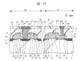
本発明者が検討したMONOS型不揮発性メモリを有する半導体装置は、図13に示すように、単結晶シリコンを母材とする半導体基板1上に、情報を電荷として蓄積する不揮発性メモリセル領域M(以下、単にメモリセル領域)と、その蓄積電荷情報を読むためのメモリゲート取り出し領域R(以下、単に取り出し領域)とを持っている。
As shown in FIG. 13, a semiconductor device having a MONOS type nonvolatile memory investigated by the present inventor has a nonvolatile memory cell region M for storing information as a charge on a
メモリセル領域Mでは、注入電荷を蓄積するONO積層絶縁膜22、その電荷注入を制御する制御ゲート電極G1、および、電荷蓄積状態によりメモリ状態を読み出すメモリゲート電極G2が形成され、これら二つのゲート電極を一対として一つのメモリセルが構成されている。この制御ゲート電極G1は、図13における紙面垂直方向Aに延在している。
In the memory cell region M, an ONO laminated
取り出し領域Rでは、メモリゲート電極G2に直接電気的な接続が取れるように水平な取り出し部Sを設け、そこにコンタクトプラグ33を接続している。通常、取り出し部Sは、延在する制御ゲート電極G1の端部におけるメモリゲート電極G2に設けられる。
In the extraction region R, a horizontal extraction portion S is provided so that electrical connection can be made directly to the memory gate electrode G2, and a
本発明者が見出した課題とは、取り出し部Sを備えたメモリゲート電極G2の製造工程に起因するものである。 The problem found by the present inventor is due to the manufacturing process of the memory gate electrode G2 having the extraction portion S.
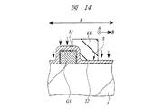
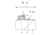
メモリセル領域Mにおけるメモリゲート電極G2のように、コントロールゲートの側壁に電極を設ける場合は、導体膜を形成した後にその全面に対してエッチング処理を施す(以下、エッチバック)ことで形成できる。一方、取り出し領域Rにおいては、メモリゲート電極G2に水平の取り出し部Sを形成する必要がある。そのため、図14に示すように、第2導体膜32のエッチバックの際に、後に水平な取り出し部Sとなる箇所をレジスト膜63により保護しておいて、エッチングを施さなければならない。このとき、フォトリソグラフィの位置合わせに余裕を持たせるため、レジスト膜63の保護領域は制御ゲート電極G1に重なるように形成される。従って、図15に示すように、取り出し領域Rのメモリゲート電極G2は、制御ゲート電極G1に乗り上げる部分P(以下、乗り上げ部)を持つように加工されるのである。
When an electrode is provided on the side wall of the control gate like the memory gate electrode G2 in the memory cell region M, it can be formed by performing an etching process on the entire surface after forming the conductor film (hereinafter referred to as etch back). On the other hand, in the extraction region R, it is necessary to form a horizontal extraction portion S in the memory gate electrode G2. Therefore, as shown in FIG. 14, when etching back the
このメモリゲート電極G2への乗り上げ部Pのように、他の部分に比して高く突出部した箇所があると、後の工程、特に周辺回路を加工する際のフォトリソグラフィ工程などで、発明者が見出した課題が生じる。 If there is a portion that protrudes higher than the other portion, such as the rising portion P on the memory gate electrode G2, the inventor in the subsequent process, particularly in the photolithography process when processing the peripheral circuit, etc. The problem found by
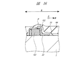
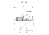
即ち、図16に示すように、周辺回路のフォトリソグラフィ工程などのために、反射防止膜53とレジスト膜64とを回転塗布すると、メモリゲート電極G2の乗り上げ部Pにおいて被覆性が悪くなり、反射防止膜53とレジスト膜64の薄い箇所ができてしまう。そして、この状態で周辺回路を加工するためのエッチングを施すと、図17に示すように、乗り上げ部Pでは、メモリゲート電極G2が露出する。更に、周辺回路の加工対象が、メモリゲート電極G2と同じ材料のゲート電極などである場合、露出したメモリゲート電極G2までもがエッチングされて、削れを起こしてしまうのである。
That is, as shown in FIG. 16, when the
このようなメモリゲート電極G2の削れは、隣接する制御ゲート電極G1とのショートの原因となるなど、本発明者が検討した半導体装置の信頼性、歩留まりの低下を引き起こしている。 Such scraping of the memory gate electrode G2 causes a short circuit with the adjacent control gate electrode G1, causing a decrease in reliability and yield of the semiconductor device studied by the present inventors.
現在、本発明者らは、図15の状態にある、制御ゲート電極G1に乗り上げたメモリゲート電極G2を覆うように酸化膜を形成するなどして、周辺回路の加工中は保護しておくことで、上記の課題を回避している。しかし、この手法では、周辺回路の加工に際してメモリ領域を覆っておく酸化膜のパターンを形成するリソグラフィ工程と、周辺回路加工後に、酸化膜を除去するためのリソグラフィ工程との、少なくとも二つのフォトリソグラフィ工程が必要となる。従って、マスクが増え、半導体装置の製造コストの増加をもたらしている。 At present, the present inventors are protecting the peripheral circuit during the processing by forming an oxide film so as to cover the memory gate electrode G2 on the control gate electrode G1 in the state of FIG. Thus, the above problem is avoided. However, in this method, at least two photolithography processes, that is, a lithography process for forming a pattern of an oxide film that covers the memory region when processing the peripheral circuit, and a lithography process for removing the oxide film after processing the peripheral circuit are performed. A process is required. Therefore, the number of masks increases, resulting in an increase in manufacturing cost of the semiconductor device.
本発明の目的は、不揮発性メモリを有する半導体装置の信頼性を向上させる技術を提供することにある。 An object of the present invention is to provide a technique for improving the reliability of a semiconductor device having a nonvolatile memory.
本発明の前記ならびにその他の目的と新規な特徴は、本明細書の記述および添付図面から明らかになるであろう。 The above and other objects and novel features of the present invention will be apparent from the description of this specification and the accompanying drawings.
本願において開示される発明のうち、代表的なものの概要を簡単に説明すれば、次のとおりである。 Of the inventions disclosed in the present application, the outline of typical ones will be briefly described as follows.
即ち、半導体基板の主面上に複数の第1ゲート電極を形成する工程と、前記半導体基板の主面上に、前記複数の第1ゲート電極を覆うように、絶縁膜を介して第2ゲート電極形成用の導体膜を堆積する工程と、前記複数の第1ゲート電極の上面上に前記第2ゲート電極形成用の導体膜が残らないように、前記第2ゲート電極形成用の導体膜をエッチングした後、残された前記第2ゲート電極形成用の導体膜をパターニングして、前記第1ゲート電極の端部側に前記第2ゲート電極と一体的に形成された導体パターンを形成する工程とを有するものである。 A step of forming a plurality of first gate electrodes on a main surface of a semiconductor substrate; and a second gate through an insulating film so as to cover the plurality of first gate electrodes on the main surface of the semiconductor substrate. A step of depositing a conductive film for forming an electrode; and a conductive film for forming the second gate electrode so that the conductive film for forming the second gate electrode does not remain on the upper surfaces of the plurality of first gate electrodes. After the etching, the remaining conductor film for forming the second gate electrode is patterned to form a conductor pattern integrally formed with the second gate electrode on the end side of the first gate electrode. It has.
また、半導体基板の主面上に第1ゲート電極を形成する工程と、前記第1ゲート電極の側壁に絶縁膜を介して第2ゲート電極を形成するとともに、前記第1ゲート電極の端部側に、前記第2ゲート電極と一体的に形成され、一部が前記第1ゲート電極の上面上に乗り上がる導体パターンを形成する工程と、前記第1ゲート電極の上面上に乗り上がる前記導体パターンの一部を除去する工程とを有するものである。 A step of forming a first gate electrode on a main surface of the semiconductor substrate; a second gate electrode is formed on a sidewall of the first gate electrode through an insulating film; and an end side of the first gate electrode Forming a conductor pattern formed integrally with the second gate electrode and partially riding on the upper surface of the first gate electrode; and the conductor pattern riding on the upper surface of the first gate electrode. And a step of removing a part of.
本願において開示される発明のうち、代表的なものによって得られる効果を簡単に説明すれば以下のとおりである。 Among the inventions disclosed in the present application, effects obtained by typical ones will be briefly described as follows.
不揮発性メモリを有する半導体装置の製造方法において、第1ゲート電極上に乗り上げる第2ゲート電極形成用の導体膜部分を除去する工程を有することにより、不揮発性メモリを有する半導体装置の信頼性を向上させることができる。 In a method of manufacturing a semiconductor device having a nonvolatile memory, the reliability of the semiconductor device having a nonvolatile memory is improved by including a step of removing a conductive film portion for forming a second gate electrode that runs on the first gate electrode. Can be made.
以下の実施の形態においては便宜上その必要があるときは、複数のセクションまたは実施の形態に分割して説明するが、特に明示した場合を除き、それらはお互いに無関係なものではなく、一方は他方の一部または全部の変形例、詳細、細く説明等の関係にある。また、以下の実施の形態において、要素の数等(個数、数値、量、範囲等を含む)に言及する場合、特に明示した場合および原理的に明らかに特定の数に限定される場合等を除き、その特定の数に限定されるものではなく、特定の数以上でも以下でも良い。さらに、以下の実施の形態において、その構成要素(要素ステップ等も含む)は、特に明示した場合および原理的に明らかに必須であると考えられる場合等を除き、必ずしも必須のものではないことは言うまでもない。同様に、以下の実施の形態において、構成要素等の形状、位置関係等に言及するときは、特に明示した場合および原理的に明らかにそうでないと考えられる場合等を除き、実質的にその形状等に近似または類似するもの等を含むものとする。このことは、上記数値および範囲についても同様である。また、本実施の形態を説明するための全図において同一機能を有するものは同一の符号を付すようにし、その繰り返しの説明は可能な限り省略するようにしている。以下、本発明の実施の形態を図面に基づいて詳細に説明する。 In the following embodiments, when it is necessary for the sake of convenience, the description will be divided into a plurality of sections or embodiments. However, unless otherwise specified, they are not irrelevant to each other. There are some or all of modifications, details, detailed explanations, and the like. Further, in the following embodiments, when referring to the number of elements (including the number, numerical value, quantity, range, etc.), especially when clearly indicated and when clearly limited to a specific number in principle, etc. Except, it is not limited to the specific number, and may be more or less than the specific number. Further, in the following embodiments, the constituent elements (including element steps and the like) are not necessarily indispensable unless otherwise specified and apparently essential in principle. Needless to say. Similarly, in the following embodiments, when referring to the shapes, positional relationships, etc. of the components, etc., the shapes are substantially the same unless otherwise specified, or otherwise apparent in principle. And the like are included. The same applies to the above numerical values and ranges. Also, components having the same function are denoted by the same reference symbols throughout the drawings for describing the embodiments, and the repetitive description thereof is omitted as much as possible. Hereinafter, embodiments of the present invention will be described in detail with reference to the drawings.
(実施の形態1)
本発明の実施の形態1では、MONOS型不揮発性メモリの製造工程において、メモリゲート電極用の導体膜のうち、制御ゲート電極上に堆積した部分を、フォトリソグラフィ工程によらずに予め除去する手法を示す。これには図1〜図8を用いて説明する。各図では、MONOS型不揮発性メモリ素子を形成する領域M(以下、単にメモリセル領域)と、そのメモリ情報を周辺回路に伝達するために取り出すための部分を形成する領域R(以下、単に取り出し領域)とにおける製造工程を同時に示す。
(Embodiment 1)
In the first embodiment of the present invention, in the manufacturing process of the MONOS type nonvolatile memory, a method of removing a portion deposited on the control gate electrode in advance in the conductive film for the memory gate electrode without using the photolithography process. Indicates. This will be described with reference to FIGS. In each figure, an area M (hereinafter simply referred to as a memory cell area) for forming a MONOS type nonvolatile memory element and an area R (hereinafter simply referred to as an extraction) for forming a portion for extracting the memory information to the peripheral circuit. The manufacturing process in (region) is shown simultaneously.
まず、図1に示すように、単結晶シリコンを母材とした半導体基板1の主面上に、後にMONOS型不揮発性メモリの制御ゲート電極の性能として要求される膜厚の、第1ゲート絶縁膜21(第1絶縁膜)、および、第1ゲート導体膜31(第1導体膜)を順に形成する。第1ゲート絶縁膜21としては、例えば酸化シリコン膜などを、第1ゲート導体膜31としては、例えば多結晶シリコンなどを用いる。
First, as shown in FIG. 1, a first gate insulation having a film thickness required later as the performance of a control gate electrode of a MONOS type nonvolatile memory is formed on a main surface of a
そして、第1ゲート導体膜31をパターニングすることにより、図1において紙面に垂直な第1方向Aに延在し、かつ、図1において紙面に水平な第2方向Bに並んで配置された、複数の制御ゲート電極G1(第1ゲート電極)を形成する。
Then, by patterning the first
本実施の形態1で製造工程を示す半導体装置においては、特に、この延在する制御ゲート電極G1の第1方向Aにおける端部にメモリゲート取り出し部(詳細は後に記述)を形成する。即ち、各図中における取り出し領域Rとは、この制御ゲート電極G1の第1方向Aにおける端部の断面を示したものである。 In the semiconductor device showing the manufacturing process in the first embodiment, in particular, a memory gate extraction portion (details will be described later) is formed at the end in the first direction A of the extending control gate electrode G1. That is, the extraction region R in each figure shows a cross section of the end portion in the first direction A of the control gate electrode G1.
その後、半導体基板1の主面側から、イオン注入法などによりドナーまたはアクセプタイオンをドープし、制御ゲート電極G1が形成されていない領域の半導体基板1表面に、後にメモリゲートのチャネル領域となる不純物導入領域4aを形成する。従って、MONOS型不揮発性メモリの蓄積電荷のキャリアとして、電子を用いる場合にはドナーイオンをドープし、ホールを用いる場合にはアクセプタイオンをドープする。以後、断りがない限り不純物導入領域を形成するためのイオン種に関しては同様とする。その後、不純物導入領域4aの表面上に形成されていた第1ゲート絶縁膜21をエッチングにより除去する。
Thereafter, from the main surface side of the
次に、半導体基板1の主面上に、制御ゲート電極G1を覆うように、酸化シリコン膜22a、窒化シリコン膜22bおよび酸化シリコン膜22cからなる積層絶縁膜22(第2絶縁膜)を形成する。これは、ONO(Oxide/Nitride/Oxide)構造を持つ積層絶縁膜22であり、MONOS型不揮発性メモリにおいて電荷の蓄積を担う層となる。その後、積層絶縁膜22を覆うように、例えば多結晶シリコンからなる第2ゲート導体膜32(第2導体膜)を形成する。これは後に、MONOS型不揮発性メモリにおいてメモリゲート電極となる。
Next, a laminated insulating film 22 (second insulating film) made of the
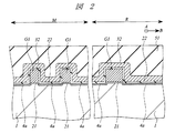
その後、図2に示すように、半導体基板1上において第2ゲート導体膜32を覆うように、例えば反射防止膜(バーク)51(保護膜)を、制御ゲート電極G1による凹凸が埋まる程度に十分厚く形成する。その後、反射防止膜51の全面に対し異方性のドライエッチング処理を施す(以下、エッチバックと記述)。
After that, as shown in FIG. 2, an antireflection film (bark) 51 (protective film), for example, is sufficiently covered with the control gate electrode G1 so as to cover the second
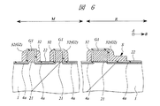
この反射防止膜51のエッチバックの際、図3に示すように、複数の制御ゲート電極G1の隣接間では反射防止膜51が残る程度でエッチバックを止める。これにより、制御ゲート電極G1の上面上の反射防止膜51を除去できる。即ち、この工程により、制御ゲート電極G1の上面上に形成された第2ゲート導体膜32が、露出することになる。
At the time of etching back the
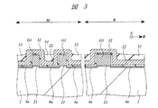
その後、図4に示すように、残った反射防止膜51をエッチングマスクとして、露出した第2ゲート導体膜32に対してエッチング処理を施すことで、制御ゲート電極G1の上面上の第2ゲート導体膜32を除去することができる。その後、反射防止膜51を除去する。
After that, as shown in FIG. 4, the exposed second
ここまでの工程により、制御ゲート電極G1の上面上の第2ゲート導体膜32が除去されたことになる。即ち、本実施の形態1によれば、本発明者が課題として見出していた、制御ゲート電極G1上に乗り上げてしまう部分の第2ゲート導体膜32を、予め除去できる。
Through the steps so far, the second
この後は、第2ゲート導体膜32をパターニングすることで、メモリゲートを形成する工程となる。
Thereafter, the second
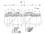
メモリセル領域Mでは、制御ゲート電極G1の側壁にメモリゲートを形成すれば良く、図5に示すように、レジスト膜によるマスクを形成せずに第2ゲート導体膜32をエッチバックする。一方、メモリゲートにコンタクトプラグを直接接続する必要があるため、取り出し領域Rにおいて第2ゲート導体膜32には、半導体基板1に対して水平な、幅広の取り出し部分を残さなければならない。従って、半導体基板1上に延在する部分の一部をレジスト膜61によってエッチングから保護しておく。
In the memory cell region M, a memory gate may be formed on the side wall of the control gate electrode G1, and as shown in FIG. 5, the second
上記図5の状態で、第2ゲート導体膜32にエッチングを施すことで、図6に示す構造が形成される。即ち、メモリセル領域Mでは、制御ゲート電極G1の側壁に、積層絶縁膜22を介して第2ゲート導体膜32が残り、メモリゲート電極G2(第2ゲート電極)が形成される。それとともに、制御ゲート電極G1の端部側の取り出し領域Rでは、レジスト膜61で保護していた部分として、半導体基板1の主面上に一部水平に延在する取り出し部Sが、メモリゲートG2と一体的な導体パターンとなるように形成される。
The structure shown in FIG. 6 is formed by etching the second
上記の工程中、取り出し領域Rにおいてメモリゲート電極G2を加工する際に、取り出し部Sを設けるために、エッチングマスクとしてレジスト膜61で保護した。その際、本発明者が検討した前述の方法と同様に、フォトリソグラフィの位置合わせに余裕を持たせるために、制御ゲート電極G1と一部重なるようにレジスト膜61が形成された(図5)。これに対して、本実施の形態1によれば、これ以前の工程で既に制御ゲート電極G1の上面上の第2ゲート導体膜32は除去されているため、制御ゲート電極G1にメモリゲート電極G2が乗り上げ、他の部分よりも高く突出する部分が形成されない。
During the above process, when processing the memory gate electrode G2 in the extraction region R, the resist
この後、周辺回路を加工することになる(図示しない)。ここで、本発明者が検討した方法によれば、周辺回路のゲート電極などを加工する際に塗布する反射防止膜およびフォトレジスト膜が、メモリ領域において制御ゲート電極上に高く突出したメモリゲート電極の箇所で薄くなり、メモリゲート電極までもが削れてしまうという現象が起きていた。更に、このようなメモリゲート電極の削れにより、制御ゲート電極とのショートを引き起こしていた。これに対し、本実施の形態1によれば、上述のように、制御ゲート電極上のメモリゲート電極は周辺回路加工の前に除去してあるため、周辺回路の加工時にメモリゲート電極が削れを起こすことは無い。 Thereafter, the peripheral circuit is processed (not shown). Here, according to the method studied by the present inventor, the memory gate electrode in which the antireflection film and the photoresist film applied when processing the gate electrode of the peripheral circuit and the like are protruded highly above the control gate electrode in the memory region There was a phenomenon in which the film became thinner and the memory gate electrode was scraped. Furthermore, such a memory gate electrode scraping causes a short circuit with the control gate electrode. On the other hand, according to the first embodiment, as described above, since the memory gate electrode on the control gate electrode is removed before the peripheral circuit processing, the memory gate electrode is scraped when the peripheral circuit is processed. There is no waking.
また、現状では、上記のようなメモリゲート電極の削れを防ぐため、周辺回路を加工している間は、メモリ領域を酸化膜などで保護していた。しかしこれは、半導体基板上に堆積した酸化膜にフォトレジストを塗布し、所望のパターンのマスクを介して露光し、現像するという一連のフォトリソグラフィ工程を、周辺回路領域の酸化膜を除去する工程と、メモリ領域の酸化膜を除去する工程との、少なくとも二回必要としていた。一方、本実施の形態1によれば、保護膜の堆積とエッチバックとによる単純な手法により上記の課題を解決できる。即ち、本実施の形態1においては、新たなマスクを用いたフォトリソグラフィ工程を導入する必要がない。これは、半導体装置の製造コストの削減に有効である。 At present, the memory region is protected with an oxide film or the like while the peripheral circuit is being processed in order to prevent the memory gate electrode from being cut as described above. However, this is a series of photolithography processes in which a photoresist is applied to an oxide film deposited on a semiconductor substrate, exposed through a mask having a desired pattern, and developed, and the oxide film in the peripheral circuit region is removed. And the step of removing the oxide film in the memory region are required at least twice. On the other hand, according to the first embodiment, the above-described problem can be solved by a simple technique by depositing a protective film and etching back. That is, in the first embodiment, it is not necessary to introduce a photolithography process using a new mask. This is effective in reducing the manufacturing cost of the semiconductor device.
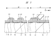
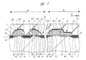
次の工程では、図7に示すように、周知の製造方法により各素子を完成させる。まず、メモリセル領域Mにおいて、二つの制御ゲート電極G1を一対として、その隣接間で対面して形成されていたメモリゲート電極G2および積層絶縁膜22を、フォトリソグラフィ法により選択的に除去する。その後、制御ゲート電極G1およびメモリゲート電極G2が形成されている領域以外の半導体基板1表面に、イオン注入法により不純物導入領域4bを形成する。ここで不純物導入領域4bは、先に形成した不純物導入領域4aと同じ極性であり、かつ、不純物導入領域4aよりも高濃度にドープするものとする。
In the next step, as shown in FIG. 7, each element is completed by a known manufacturing method. First, in the memory cell region M, the two control gate electrodes G1 are paired, and the memory gate electrode G2 and the laminated insulating
続いて、制御ゲート電極G1またはメモリゲート電極G2の側壁に、絶縁体からなるスペーサ23を形成する。これらは、スペーサ23用の絶縁膜を基板表面に形成し、エッチバックすることで形成する。スペーサ23用の絶縁膜としては、例えば酸化シリコン膜/窒化シリコン膜/酸化シリコン膜の積層構造などを用いる。
Subsequently, a
その後、メモリセル領域MにおいてMONOS型不揮発性メモリと、後に形成する金属配線とのコンタクト領域を形成するために、イオン注入法により不純物導入領域4cを形成する。ここで不純物導入領域4cは、先に形成した不純物導入領域4a,4bと同じ極性であり、かつ、不純物導入領域4bよりも高濃度にドープするものとする。続いて、不純物導入領域4c,制御ゲート電極G1およびメモリゲート電極G2の取り出し部Sそれぞれの表面に、金属配線とのオーミック接続を目的としたシリサイド層7の形成を行う。シリサイド層7は以下の周知の方法により形成できる。まず、シリサイドの対象となる金属(例えばコバルト)を、スパッタ法により半導体基板1の表面に堆積する。続いて熱処理を施すことで、絶縁膜を介さずにシリコンと金属が接している不純物導入領域4c表面、制御ゲート電極G1上面およびメモリゲート電極G2の取り出し部S表面において、金属とシリコンの合金化が進み、シリサイド層7が形成される。
Thereafter, in order to form a contact region between the MONOS type nonvolatile memory and a metal wiring to be formed later in the memory cell region M, an
その後、絶縁膜24として、例えば窒化シリコン膜を半導体基板1表面全体に形成する。続いて、各素子の上部に形成される金属配線の層間絶縁膜25として、例えば酸化シリコン膜を形成する。
Thereafter, as the insulating
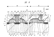
この後の工程は、周知の方法による金属配線工程となる。まず、図8に示すように、層間絶縁膜25にコンタクトホールH1を形成した後、金属(例えばタングステン)膜を堆積し、表面研磨することで、各素子への金属コンタクトプラグ33を形成する。その後、配線層を形成するための絶縁膜26を形成し、配線パターンH2をフォトリソグラフィ法により形成する。続いて、スパッタ法などにより金属(例えば銅)を堆積し、表面研磨することで、配線パターンH2中に金属配線34を形成する。
The subsequent process is a metal wiring process by a known method. First, as shown in FIG. 8, after forming a contact hole H1 in the
この工程により、取り出し領域Rにおいて、メモリゲート電極G2からの取り出し部Sに、金属コンタクトプラグ33が接続されることになる。
By this step, the
その後同様の工程を繰り返すことで上部金属配線を形成し、本実施の形態1による半導体装置が完成する。 Thereafter, similar processes are repeated to form the upper metal wiring, and the semiconductor device according to the first embodiment is completed.
本実施の形態1によれば、MONOS型不揮発性メモリを有する半導体装置の製造工程において、メモリゲート電極G2用の第2ゲート導体膜32を形成した直後に、フォトリソグラフィ工程に依らずに、制御ゲート電極G1上の第2ゲート導体膜32を除去できる。これにより、メモリ取り出し領域Rにおいて、制御ゲート電極G1上にメモリゲート電極G2が乗り上げることが無い。従って、後の工程で、メモリゲート電極に局所的な削れが起こり、制御ゲート電極とショートしてしまうなど、信頼性を損ねる要因を排除できる。
According to the first embodiment, in the manufacturing process of the semiconductor device having the MONOS type nonvolatile memory, the control is performed immediately after the second
(実施の形態2)
上記実施の形態1では、MONOS型不揮発性メモリを有する半導体装置の製造工程において、制御ゲート電極上に堆積したメモリゲート用の導体膜を、メモリゲート電極の加工前に除去する手法を示した。
(Embodiment 2)
In the first embodiment, the method of removing the memory gate conductive film deposited on the control gate electrode before the processing of the memory gate electrode in the manufacturing process of the semiconductor device having the MONOS type nonvolatile memory has been described.
本実施の形態2では、通常の方法でメモリゲート電極を加工した後に、制御ゲート電極に乗り上げたメモリゲート電極を選択的に除去する手法を、図9〜図12を用いて示す。 In the second embodiment, a method of selectively removing the memory gate electrode that has been placed on the control gate electrode after processing the memory gate electrode by a normal method will be described with reference to FIGS.
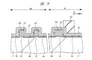
まず、上記実施の形態1において図1を用いて説明した方法と同様にして、図9に示すように、半導体基板1の主面上に形成した制御ゲート電極G1を、電荷蓄積用の積層絶縁膜22およびメモリゲート電極用の第2ゲート導体膜32で覆った構造を形成する。
First, in the same manner as the method described with reference to FIG. 1 in the first embodiment, as shown in FIG. 9, the control gate electrode G1 formed on the main surface of the
その後、本発明者が検討した方法と同様に、メモリゲート電極を加工する工程に入る。即ち、メモリセル領域Mでは、第2ゲート導体膜32をそのままエッチバックし、取り出し領域Rでは、メモリゲートに半導体基板1上の一部に延在する取り出し部を設けるため、水平な部分をレジスト膜62で覆い、第2ゲート導体膜32にエッチングを施す。
Thereafter, the memory gate electrode is processed in the same manner as the method examined by the present inventors. That is, in the memory cell region M, the second
このとき、フォトリソグラフィの位置合わせに余裕を持たせるため、レジスト膜62の保護領域は制御ゲート電極G1に一部重なるように形成する。
At this time, the protection region of the resist
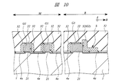
続いて、図9の状態で第2導体膜32に対してエッチングを施すことで、図10に示す構造となる。即ち、メモリセル領域Mでは、制御ゲート電極G1の側壁に、積層絶縁膜22を介して第2ゲート導体膜32が残り、メモリゲート電極G2(第2ゲート電極)が形成される。それとともに、制御ゲート電極G1の端部側の取り出し領域Rでは、レジスト膜62で保護していた部分として、制御ゲート電極G1の上面上に部分的に乗り上げた状態で、かつ、半導体基板1の主面上に一部水平に延在する取り出し部Sが、メモリゲートG2と一体的な導体パターンとなるように形成される。
Subsequently, the structure shown in FIG. 10 is obtained by etching the
上記のように、この段階では、本発明者が検討した方法と同様に、フォトリソグラフィの都合上、取り出し領域Rにおいて、制御ゲート電極G1上の一部にメモリゲート電極G2が乗り上げている。 As described above, at this stage, similarly to the method studied by the present inventors, the memory gate electrode G2 is placed on a part of the control gate electrode G1 in the extraction region R for the convenience of photolithography.
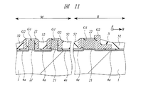
続いて、本実施の形態2では、これまでの工程で半導体基板1上に形成した制御ゲート電極G1およびメモリゲート電極G2を覆うように、例えば反射防止膜(バーク)52(保護膜)を、制御ゲート電極G1およびメモリゲート電極G2による凹凸が埋まる程度に十分厚く形成する。その後、反射防止膜52をエッチバックする。
Subsequently, in the second embodiment, for example, an antireflection film (bark) 52 (protective film) is formed so as to cover the control gate electrode G1 and the memory gate electrode G2 formed on the
この反射防止膜52のエッチバックの際、図11に示すように、複数の制御ゲート電極G1の隣接間において反射防止膜52が残るように、エッチバックを止める。これにより、制御ゲート電極G1の上面上の反射防止膜52を除去できる。即ち、この工程により、取り出し領域Rに形成された第2ゲート導体膜32のうち、取り出し領域Rの制御ゲート電極G1の上面上に一部乗り上げて形成された部分が露出することになる。
When this
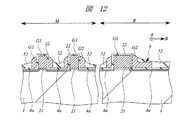
その後、図12に示すように、残された反射防止膜52をエッチングマスクとして、露出した第2ゲート導体膜32に対してエッチング処理を施すことにより、制御ゲート電極G1の上面上に一部乗り上げていた第2ゲート導体膜32を除去することができる。
Thereafter, as shown in FIG. 12, the exposed second
このように、本実施の形態2の手法によれば、本発明者が課題として見出していた、制御ゲート電極G1上に乗り上げてしまう部分の第2ゲート電極G2を、選択的に除去できるのである。更に、本手法は膜形成とエッチバックとによるものであるから、マスクを用いたフォトリソグラフィ工程の追加を必要としない。 As described above, according to the method of the second embodiment, the second gate electrode G2 that has been found on the control gate electrode G1 and found as a problem by the inventor can be selectively removed. . Furthermore, since this method is based on film formation and etch back, it does not require the addition of a photolithography process using a mask.
続いて、エッチングマスクとして残した反射防止膜52を除去すれば、上記実施の形態1において図6に示した構造と同じ構造が形成される。即ち、半導体基板1上に、メモリセル領域Mにおいては制御ゲート電極G1と、電荷蓄積のための積層絶縁膜22を介してメモリゲート電極G2とを形成し、取り出し領域Rにおいては、制御ゲート電極G1に乗り上げず、かつ取り出し部Sを備えるようなメモリゲート電極G2を形成した。
Subsequently, if the
その後のMONOS型不揮発性メモリ素子を完成するための工程、それらに接続される配線を形成する工程、およびその工程により形成される構造は、上記実施の形態1において図7および図8を用いて説明した工程および構造と同様であり、ここでの説明は省略する。 The subsequent process for completing the MONOS type nonvolatile memory element, the process for forming the wiring connected thereto, and the structure formed by the process will be described with reference to FIGS. 7 and 8 in the first embodiment. This is the same as the process and structure described, and a description thereof is omitted here.
以上、本発明者によってなされた発明を実施の形態に基づき具体的に説明したが、本発明は前記実施の形態に限定されるものではなく、その要旨を逸脱しない範囲で種々変更可能であることはいうまでもない。 As mentioned above, the invention made by the present inventor has been specifically described based on the embodiment. However, the present invention is not limited to the embodiment, and various modifications can be made without departing from the scope of the invention. Needless to say.
例えば、上記実施の形態1,2において、制御ゲート電極G1上の第2ゲート導体膜32またはメモリゲート電極G2を選択的に除去するために形成した保護膜として、反射防止膜51,52を用いたが、メモリゲート電極G2用の第2ゲート導体膜32のエッチング速度に対して十分な選択比を持つ材料を用いることでも、同様の効果が得られる。
For example, in the first and second embodiments, the
本発明は、半導体装置の製造方法に適用して有効であり、特に、MONOS型不揮発性メモリを有する半導体装置の製造に効果的である。 The present invention is effective when applied to a method for manufacturing a semiconductor device, and is particularly effective for manufacturing a semiconductor device having a MONOS type nonvolatile memory.
1 半導体基板
21 第1ゲート絶縁膜(第1絶縁膜)
22 積層絶縁膜(第2絶縁膜)
31 第1ゲート導体膜(第1導体膜)
32 第2ゲート導体膜(第2導体膜)
51 反射防止膜(保護膜)
52 反射防止膜(保護膜)
M メモリセル領域
R 取り出し領域
S 取り出し部
A 第1方向
B 第2方向
G1 制御ゲート電極(第1ゲート電極)
G2 メモリゲート電極(第2ゲート電極)
DESCRIPTION OF
22 Multilayer insulation film (second insulation film)
31 1st gate conductor film (1st conductor film)
32 Second gate conductor film (second conductor film)
51 Antireflection film (protective film)
52 Anti-reflective coating (protective coating)
M memory cell region R extraction region S extraction portion A first direction B second direction G1 control gate electrode (first gate electrode)
G2 Memory gate electrode (second gate electrode)
Claims (4)
(a)半導体基板の主面上に、第1絶縁膜および第1導体膜を順に形成する工程、
(b)前記第1導体膜をパターニングすることにより、前記半導体基板の主面における第1方向に延在し、かつ、前記第1方向に交差する第2方向に並んで配置された複数の第1ゲート電極を形成する工程、
(c)前記(b)工程後、前記半導体基板の主面上に、前記複数の第1ゲート電極を覆うように、第2絶縁膜および第2導体膜を順に形成する工程、
(d)前記(c)工程後、前記半導体基板の主面上に、前記第2導体膜を覆うように保護膜を形成した後、前記保護膜に対してエッチング処理を施すことにより、前記複数の第1ゲート電極の隣接間では前記保護膜が残るように、前記保護膜を除去する工程、
(e)前記(d)工程後、前記保護膜をエッチングマスクとして前記第2導体膜に対してエッチング処理を施すことにより、前記複数の第1ゲート電極の上面上の前記第2導体膜を除去する工程、
(f)前記(e)工程後、前記保護膜を除去した後、前記第2導体膜をパターニングすることにより、
前記複数の第1ゲート電極の側壁に、前記第2絶縁膜を介して第2ゲート電極を形成するとともに、前記複数の第1ゲート電極の端部側に、前記半導体基板の主面上に一部延在する取り出し部を、前記第2ゲート電極と一体的な導体パターンとなるように形成する工程。 A method for manufacturing a semiconductor device comprising the following steps:
(A) a step of sequentially forming a first insulating film and a first conductor film on the main surface of the semiconductor substrate;
(B) By patterning the first conductor film, a plurality of first conductors extending in the first direction on the main surface of the semiconductor substrate and arranged in a second direction intersecting the first direction are arranged. Forming one gate electrode;
(C) After the step (b), a step of sequentially forming a second insulating film and a second conductor film on the main surface of the semiconductor substrate so as to cover the plurality of first gate electrodes;
(D) After the step (c), a protective film is formed on the main surface of the semiconductor substrate so as to cover the second conductive film, and then the protective film is subjected to an etching process, whereby the plural Removing the protective film so that the protective film remains between adjacent first gate electrodes of
(E) After the step (d), the second conductor film on the upper surfaces of the plurality of first gate electrodes is removed by performing an etching process on the second conductor film using the protective film as an etching mask. The process of
(F) After the step (e), after removing the protective film, by patterning the second conductor film,
A second gate electrode is formed on a side wall of the plurality of first gate electrodes via the second insulating film, and is formed on the main surface of the semiconductor substrate on the end side of the plurality of first gate electrodes. A step of forming the extending portion extending so as to be a conductor pattern integral with the second gate electrode;
(a)半導体基板の主面上に、第1絶縁膜および第1導体膜を順に形成する工程、
(b)前記第1導体膜をパターニングすることにより、前記半導体基板の主面における第1方向に延在し、かつ、前記第1方向に交差する第2方向に並んで配置された複数の第1ゲート電極を形成する工程、
(c)前記(b)工程後、前記半導体基板の主面上に、前記複数の第1ゲート電極を覆うように、第2絶縁膜および第2導体膜を順に形成する工程、
(d)前記(c)工程後、前記第2導体膜をパターニングすることにより、
前記複数の第1ゲート電極の側壁に、前記第2絶縁膜を介して第2ゲート電極を形成するとともに、前記複数の第1ゲート電極の端部側に、前記複数の第1ゲート電極の端部の上面上に部分的に乗り上げた状態で、かつ、前記半導体基板の主面上に一部延在する取り出し部を、前記第2ゲート電極と一体的な導体パターンとなるように形成する工程、
(e)前記(d)工程後、前記半導体基板の主面上に、前記複数の第1ゲート電極および前記第2ゲート電極を覆うように保護膜を形成した後、前記保護膜に対してエッチング処理を施すことにより、前記複数の第1ゲート電極の隣接間に前記保護膜が残るように、前記保護膜を除去する工程、
(f)前記(e)工程後、前記保護膜をエッチングマスクとして、前記第2ゲート電極取り出し用の導体パターンにおいて、前記複数の第1ゲート電極の端部の上面上に部分的に乗り上げている部分を除去する工程。 A method for manufacturing a semiconductor device comprising the following steps:
(A) a step of sequentially forming a first insulating film and a first conductor film on the main surface of the semiconductor substrate;
(B) By patterning the first conductor film, a plurality of first conductors extending in the first direction on the main surface of the semiconductor substrate and arranged in a second direction intersecting the first direction are arranged. Forming one gate electrode;
(C) After the step (b), a step of sequentially forming a second insulating film and a second conductor film on the main surface of the semiconductor substrate so as to cover the plurality of first gate electrodes;
(D) After the step (c), by patterning the second conductor film,
A second gate electrode is formed on a side wall of the plurality of first gate electrodes via the second insulating film, and an end of the plurality of first gate electrodes is formed on an end side of the plurality of first gate electrodes. Forming a take-out part that partially rides on the upper surface of the part and partially extending on the main surface of the semiconductor substrate so as to form a conductor pattern integral with the second gate electrode; ,
(E) After the step (d), a protective film is formed on the main surface of the semiconductor substrate so as to cover the plurality of first gate electrodes and the second gate electrode, and then etched on the protective film. Removing the protective film so that the protective film remains between adjacent ones of the plurality of first gate electrodes by performing a treatment;
(F) After the step (e), using the protective film as an etching mask, the conductive pattern for taking out the second gate electrode partially rides on the upper surfaces of the end portions of the plurality of first gate electrodes. Removing the portion.
前記複数の第1ゲート電極は制御ゲート電極であり、
前記第2ゲート電極はメモリゲート電極であり、
前記第2絶縁膜は情報の記憶に寄与する電荷蓄積層であることを特徴とする半導体装置の製造方法。 In the manufacturing method of the semiconductor device of Claim 1 or 2,
The plurality of first gate electrodes are control gate electrodes;
The second gate electrode is a memory gate electrode;
The method of manufacturing a semiconductor device, wherein the second insulating film is a charge storage layer contributing to information storage.
前記第2絶縁膜は酸化膜、窒化膜および酸化膜の積層膜であり、
前記保護膜は反射防止膜であることを特徴とする半導体装置の製造方法。 In the manufacturing method of the semiconductor device of Claim 1, 2, or 3,
The second insulating film is a laminated film of an oxide film, a nitride film and an oxide film,
The method for manufacturing a semiconductor device, wherein the protective film is an antireflection film.
Priority Applications (1)
| Application Number | Priority Date | Filing Date | Title |
|---|---|---|---|
| JP2006350933A JP2008166325A (en) | 2006-12-27 | 2006-12-27 | Method of manufacturing semiconductor device |
Applications Claiming Priority (1)
| Application Number | Priority Date | Filing Date | Title |
|---|---|---|---|
| JP2006350933A JP2008166325A (en) | 2006-12-27 | 2006-12-27 | Method of manufacturing semiconductor device |
Publications (1)
| Publication Number | Publication Date |
|---|---|
| JP2008166325A true JP2008166325A (en) | 2008-07-17 |
Family
ID=39695461
Family Applications (1)
| Application Number | Title | Priority Date | Filing Date |
|---|---|---|---|
| JP2006350933A Pending JP2008166325A (en) | 2006-12-27 | 2006-12-27 | Method of manufacturing semiconductor device |
Country Status (1)
| Country | Link |
|---|---|
| JP (1) | JP2008166325A (en) |
Cited By (2)
| Publication number | Priority date | Publication date | Assignee | Title |
|---|---|---|---|---|
| JP2010153780A (en) * | 2008-12-24 | 2010-07-08 | Dongbu Hitek Co Ltd | Method of manufacturing flash memory device |
| JP2011222938A (en) * | 2009-10-28 | 2011-11-04 | Renesas Electronics Corp | Semiconductor device and method for manufacturing the same |
-
2006
- 2006-12-27 JP JP2006350933A patent/JP2008166325A/en active Pending
Cited By (2)
| Publication number | Priority date | Publication date | Assignee | Title |
|---|---|---|---|---|
| JP2010153780A (en) * | 2008-12-24 | 2010-07-08 | Dongbu Hitek Co Ltd | Method of manufacturing flash memory device |
| JP2011222938A (en) * | 2009-10-28 | 2011-11-04 | Renesas Electronics Corp | Semiconductor device and method for manufacturing the same |
Similar Documents
| Publication | Publication Date | Title |
|---|---|---|
| KR100432888B1 (en) | Non-volitile memory device and method thereof | |
| US20090212345A1 (en) | Semiconductor Device and Method for Manufacturing the Same | |
| US6255155B1 (en) | Nonvolatile memory and method for fabricating the same | |
| JP4773073B2 (en) | Manufacturing method of semiconductor device | |
| US6258669B1 (en) | Methods and arrangements for improved formation of control and floating gates in non-volatile memory semiconductor devices | |
| US7883952B2 (en) | Method of manufacturing flash memory device | |
| US6034395A (en) | Semiconductor device having a reduced height floating gate | |
| JP2008047863A (en) | Manufacturing method of well pickup structure of nonvolatile memory | |
| US7439577B2 (en) | Semiconductor memory and method for manufacturing the same | |
| CN101236928A (en) | Method for manufacturing non-volatile memory | |
| US7390714B2 (en) | Method of manufacturing semiconductor device having tungsten gates electrode | |
| CN101026128A (en) | Method of manufacturing non-volatile memory device | |
| US7670904B2 (en) | Nonvolatile memory device and method for fabricating the same | |
| JP2008166325A (en) | Method of manufacturing semiconductor device | |
| JPH07106441A (en) | Fabrication of semiconductor device | |
| KR100317318B1 (en) | Nonvolatile memory device and method for fabricating the same | |
| KR100580118B1 (en) | Method for forming gate electrode pattern of semiconductor device | |
| CN105810682A (en) | Non-volatile storage unit, NAND-type non-volatile memory and manufacturing method thereof | |
| KR20090074332A (en) | Manufacturing Method of Semiconductor Device | |
| US20050230738A1 (en) | NAND type flash memory device, and method for manufacturing the same | |
| US7169672B1 (en) | Split gate type nonvolatile memory device and manufacturing method thereof | |
| KR101072661B1 (en) | Non-volatile memory device and manufacturing method thereof | |
| US20140070297A1 (en) | Semiconductor storage device and fabrication method thereof | |
| CN100536116C (en) | Method for manufacturing well region extension structure of nonvolatile memory | |
| KR20040029525A (en) | Flash memory device and method for manufacturing the same |