JP2008042017A - Resist peeling and removing method capable of recovering resist and semiconductor manufacturing device using it - Google Patents
Resist peeling and removing method capable of recovering resist and semiconductor manufacturing device using it Download PDFInfo
- Publication number
- JP2008042017A JP2008042017A JP2006215979A JP2006215979A JP2008042017A JP 2008042017 A JP2008042017 A JP 2008042017A JP 2006215979 A JP2006215979 A JP 2006215979A JP 2006215979 A JP2006215979 A JP 2006215979A JP 2008042017 A JP2008042017 A JP 2008042017A
- Authority
- JP
- Japan
- Prior art keywords
- resist film
- resist
- liquid
- film
- laser
- Prior art date
- Legal status (The legal status is an assumption and is not a legal conclusion. Google has not performed a legal analysis and makes no representation as to the accuracy of the status listed.)
- Pending
Links
Images


Abstract
Description
本発明は、半導体ウェハ基板等に塗布されたレジスト膜を回収可能に剥離除去する方法及びそれを用いる半導体製造装置に関する。 The present invention relates to a method for recovering and removing a resist film applied to a semiconductor wafer substrate and the like and a semiconductor manufacturing apparatus using the method.
半導体製造プロセスの中枢であるフォトリソグラフィ工程は一般にウェハ基板上へのi)フォトレジスト塗布、ii)露光、iii)現像、iv)エッチング、v)使用済みレジスト除去の5工程を経て行っている。半導体デバイス製造ではこれらの工程を20〜30回繰り返している。 The photolithography process, which is the core of the semiconductor manufacturing process, is generally carried out through five steps: i) photoresist application, ii) exposure, iii) development, iv) etching, and v) used resist removal. In semiconductor device manufacturing, these steps are repeated 20 to 30 times.
フォトレジスト材料は環化−ビスアジド系、DNQ(ジアゾナフトキノン)−ノボラック樹脂系、PMMA(ポリメチルメタクリエート)系等さまざまな種類が存在する。これらは半導体ウェハ基板の性質、微細化条件、エッチング条件にあわせて設定使用されている。上記工程中、v)使用済みのフォトレジストの除去にはウェット方式とドライ方式が用いられる。ウェット方式ではフォトレジストは有機物であることから硫酸などの酸化性の酸で処理できるが、高温高濃度条件下で処理する為半導体ウェハ基板の性質や下地膜の状態によっては使用できない場合がある。そこで各フォトレジストにあわせた市販のレジスト剥離液が用いられる。この液は基本的に有機アルカリ系の混液でありエチレンジアミンやピロカテコールなどが含まれているが、詳細な化学組成は明らかにされていない。 There are various types of photoresist materials such as cyclized-bisazide, DNQ (diazonaphthoquinone) -novolak resin, PMMA (polymethyl methacrylate). These are set and used in accordance with the properties of the semiconductor wafer substrate, miniaturization conditions, and etching conditions. During the above steps, v) a wet method and a dry method are used to remove the used photoresist. In the wet method, since the photoresist is an organic substance, it can be treated with an oxidizing acid such as sulfuric acid. However, since the photoresist is treated under high temperature and high concentration conditions, it may not be used depending on the properties of the semiconductor wafer substrate and the state of the underlying film. Therefore, a commercially available resist stripping solution suitable for each photoresist is used. This liquid is basically an organic alkaline mixed liquid and contains ethylenediamine, pyrocatechol and the like, but the detailed chemical composition is not clarified.
レジストの除去はコスト面から主にこのウェット方式により処理されているが、デバイス製造では上述したようにかかるレジスト剥離除去が20〜30回繰り返されるため、大量の化学廃液が発生する。そのため、環境負荷低減が要求される現代においてはウェット処理以外の手法が望まれている。 The removal of the resist is mainly processed by this wet method from the viewpoint of cost. However, since the resist stripping and removal are repeated 20 to 30 times as described above in device manufacturing, a large amount of chemical waste liquid is generated. Therefore, techniques other than wet treatment are desired in the present day when environmental load reduction is required.
一方、ドライ方式ではプラズマ、UV、オゾン等を用いた処理であり、反応生成物はCO2とH2Oであることから環境負荷の面においては優位な点はあるが、ドライ方式のみではフォトレジストの残渣までの完全除去は困難であり、ウェット処理との併用は避けられない状況にある。また省エネ・生産性向上という面においてはまだまだ課題が残っている。 On the other hand, the dry method is a process using plasma, UV, ozone, etc., and the reaction products are CO 2 and H 2 O. It is difficult to completely remove the resist residue, and the combined use with the wet treatment is inevitable. In addition, there are still problems in terms of energy saving and productivity improvement.
そこで、短波長のレーザを用いて、光解離を伴ったアブレーションによりレジスト膜を除去することが試みられている(特許文献1、2参照)。当該除去方法では、大量の化学廃液が発生しないため環境負荷が低減されている。
しかしながら、レジスト膜のアブレーションによる除去方法(特許文献1及び2)においては、レジスト膜を構成する有機物の結合手を切断することができる短波長のレーザ光が必要となるが、短波長のレーザ光はフォトンコストが高いため経済的ではない。また、レジスト膜が短波長のレーザ光の照射によるアブレーションにより分解するため、レジストの再使用は困難であり、しかもレーザ光分解したレジスト膜を含む洗浄液は廃液として処理しなければならないという問題点がある。なお、ここで、アブレーションとはレーザ光をレンズで集光などして、金属、無機化合物、高分子など様々な物質にある一定の強度(閾値)以上で照射すると、それらの物質表面から様々な粒子が飛び出し、物質表面がエッチングされる現象をいい、有機高分子であるレジスト膜では光解離が起こる。 However, in the removal method by ablation of the resist film (Patent Documents 1 and 2), a short-wavelength laser beam capable of cutting a bond of an organic substance constituting the resist film is required. Is not economical due to high photon cost. Further, since the resist film is decomposed by ablation by irradiation with short-wavelength laser light, it is difficult to reuse the resist, and the cleaning liquid containing the resist film decomposed by laser light must be treated as a waste liquid. is there. Here, the ablation means that various kinds of materials such as metals, inorganic compounds, and polymers are irradiated with a certain intensity (threshold) or more by condensing laser light with a lens. This is a phenomenon in which particles pop out and the surface of a material is etched. Photodissociation occurs in a resist film that is an organic polymer.
そこで、本発明は、第1に、フォトンコストの高いレーザ光を使用することなく、安価に、しかもウェハ基板に損傷を与えることなく、レジスト膜を剥離除去することができる方法を提供することを目的とする。第2に、本発明は、レジストがアブレーションを起こすことなくレジスト膜をウェハ面から剥離させ、そのアブレーションを起こしていないレジスト膜を洗浄液から容易に分離回収することができ、廃液処理問題を解消することができる方法を提供することにある。 Accordingly, the present invention firstly provides a method capable of peeling and removing a resist film at low cost and without damaging the wafer substrate without using laser light with high photon cost. Objective. Secondly, the present invention can remove the resist film from the wafer surface without causing the ablation of the resist, and can easily separate and recover the resist film that has not been ablated from the cleaning liquid, thereby eliminating the waste liquid processing problem. It is to provide a method that can.
本発明者らは、鋭意研究を行った結果、フォトンコストの安い長波長のレーザ光を用いると、ノボラック系レジストにおいてはレジスト表面でアブレーションを起こさず、当該レジストを透過するが、ウェハ基板のレーザ光吸収により、レジスト膜下のウェハ基板に損傷を与えてしまうという問題がある。そこで、ウェハ基板に損傷を与えない程度の閾値に低減すると、長波長のレーザ光では、レジスト膜とウェハ基板の界面で発生する熱は僅かとなって、その熱応力だけではレジスト膜をウェハ基板から剥離除去することは困難であった。
しかしながら、レジスト表面上に水などのレーザ光が透過する液体膜の壁を存在させ、その状態でウェハ基板にレーザ光を照射すれば、照射したレーザ光のエネルギーによりウェハ基板が加熱され、さらにはその熱拡散により、上記ウェハ基板に付着しているレジストと液体界面では、液体自身の局所的な沸騰・蒸発によりウェハと液体を反対方向に押しのける力の反作用(レジスト側への力)によりレジスト膜が衝撃を受けレジスト膜をウェハ基板から剥離することができることを見出し、本発明を完成するに至った。
As a result of intensive studies, the inventors of the present invention, when using a long wavelength laser beam with low photon cost, a novolak resist does not cause ablation on the resist surface, but passes through the resist. There is a problem that the wafer substrate under the resist film is damaged by light absorption. Therefore, if the threshold is reduced to a level that does not damage the wafer substrate, the heat generated at the interface between the resist film and the wafer substrate becomes small with long-wavelength laser light. It was difficult to peel and remove from.
However, if there is a wall of a liquid film through which a laser beam such as water is transmitted on the resist surface and the wafer substrate is irradiated with the laser beam in that state, the wafer substrate is heated by the energy of the irradiated laser beam. Due to the thermal diffusion, at the resist-liquid interface adhering to the wafer substrate, the resist film is caused by the reaction (force on the resist side) of the force that pushes the wafer and the liquid in the opposite directions by local boiling / evaporation of the liquid itself. Has been found that the resist film can be peeled off from the wafer substrate upon impact, and the present invention has been completed.
したがって、本発明は、ウェハ基板を含む基板上に形成されたレジスト膜を剥離除去するにあたり、レジスト膜を透過可能であってウェハ基板に吸収可能なレーザ光を選択する一方、レジスト膜上にレーザ光を透過可能な液体膜を形成し、該液体膜を介して上記選択されたレーザ光をレジスト膜に照射して上記レジスト表面で実質的にアブレーションを起こさせることなく、レジスト膜を透過させて上記ウェハ基板とレジスト膜との界面でウェハ表面に損傷を与えない程度の熱を発生させる一方、上記レジスト膜表面と液体との界面で上記液体膜を局所的に沸騰・蒸発させ、上記レジスト膜に衝撃を与えて剥離させることを特徴とするレジスト膜剥離除去方法にある。 Therefore, in the present invention, when removing the resist film formed on the substrate including the wafer substrate, a laser beam that can be transmitted through the resist film and absorbed by the wafer substrate is selected, while a laser beam on the resist film is selected. A liquid film capable of transmitting light is formed, and the resist film is irradiated through the liquid film to cause the resist film to pass through without substantially causing ablation on the resist surface. Heat is generated at the interface between the wafer substrate and the resist film so as not to damage the wafer surface, and the liquid film is locally boiled and evaporated at the interface between the resist film surface and the liquid. The resist film is peeled and removed by applying a shock to the resist film.
本発明においては、上記レジスト膜に対してアブレーションを起こさないレーザ光を選択することが第1条件である。したがって、レーザ光のレジスト膜の透過率は重要であり、レジスト膜との透過率の関係は20%以上である必要がある。例えば、ノボラック系ポジ型レジストのUV透過率は、図12に示すように300nm未満では極端に低いが、400nmを超えると上昇し、500nm付近から80%を超えることになる。したがって、レジスト膜との透過効果との関係を見て選択する波長が決定される。レーザ光の場合、長波長側のフォトンコストが安くなる傾向になる。 In the present invention, the first condition is to select a laser beam that does not cause ablation to the resist film. Therefore, the transmittance of the resist film for laser light is important, and the transmittance relationship with the resist film needs to be 20% or more. For example, as shown in FIG. 12, the UV transmittance of a novolac positive resist is extremely low below 300 nm, but increases above 400 nm and exceeds 80% from around 500 nm. Therefore, the wavelength to be selected is determined in view of the relationship with the transmission effect with the resist film. In the case of laser light, the photon cost on the long wavelength side tends to be reduced.
上記レーザ光照射によりレジスト膜の剥離が起こるが、電気的または機械的振動をレーザ光照射時及び/又は照射後レジスト膜に付与することにより剥離効率を向上させることが見出されており、併用することにより照射するレーザ光の照射エネルギーを低減させることが可能である。かかる振動はレーザ照射時はレジスト膜上に形成する液体膜を介してまたはレーザ照射後はレジスト膜上に存在する洗浄液を介して付与するのが適当であり、超音波振動装置を用い、機械的振動を付与することができる。上記超音波振動の強度は上記レーザ光によるレジスト膜の剥離を補助するものであるから、レーザ光の照射エネルギー量を考慮して調整するのが好ましい。他方、上記レジスト膜を透過するレーザ光の照射エネルギーは照射時間とレーザ光のパルス幅によって決まる。したがって、上記レジスト表面で実質的にアブレーションが起こらないでかつ、ウェハ基板に対して損傷閾値以下のエネルギー量となるフェムト秒からミリ秒のパルス幅の範囲でレーザ光を選択する。 Although the resist film is peeled off by the above laser beam irradiation, it has been found that by applying electrical or mechanical vibration to the resist film at the time of laser beam irradiation and / or after irradiation, the stripping efficiency can be improved. By doing so, it is possible to reduce the irradiation energy of the laser beam to be irradiated. It is appropriate to apply such vibration through a liquid film formed on the resist film during laser irradiation or through a cleaning liquid existing on the resist film after laser irradiation. Vibration can be applied. Since the intensity of the ultrasonic vibration assists the peeling of the resist film by the laser beam, it is preferably adjusted in consideration of the irradiation energy amount of the laser beam. On the other hand, the irradiation energy of the laser light transmitted through the resist film is determined by the irradiation time and the pulse width of the laser light. Therefore, the laser beam is selected within the range of the femtosecond to millisecond pulse width that causes substantially no ablation on the resist surface and has an energy amount equal to or less than the damage threshold for the wafer substrate.
本発明方法においては、上記レーザ光による剥離効果の蓄積が見られるので、照射回数を多くすればするほどレーザ光の照射エネルギーを低減設定することができる。 In the method of the present invention, since the accumulation of the peeling effect by the laser beam is seen, the irradiation energy of the laser beam can be set to decrease as the number of irradiations is increased.
本発明において、上記レジスト膜上に形成される液体膜が、レーザ光を透過可能であって、局所加熱により沸騰、蒸発可能である必要がある。上記液体膜はレーザ光の照射によってレジスト膜の剥離増加を発揮するので、従来のように、レジスト膜を溶解する必要がなく、水、水溶液或いは水分散液からなることができる。液体膜が形成されやすいように表面張力を降下させる界面活性剤等を添加してもよい。上記レジスト膜上に形成される液体膜の膜厚はレーザ光照射エネルギー強度、レーザ光照射回数、上記振動強度などの剥離効果を考慮して決定されるのがよい。また、上記レジスト膜上に形成される液体膜の温度を通常液温より高くまたは低く設定する方が剥離効果を向上させる場合がある。 In the present invention, the liquid film formed on the resist film needs to be able to transmit laser light and be able to boil and evaporate by local heating. Since the liquid film exhibits increased peeling of the resist film upon irradiation with laser light, it is not necessary to dissolve the resist film as in the prior art, and can be made of water, an aqueous solution, or an aqueous dispersion. A surfactant or the like that lowers the surface tension may be added so that a liquid film is easily formed. The film thickness of the liquid film formed on the resist film is preferably determined in consideration of peeling effects such as laser beam irradiation energy intensity, the number of laser beam irradiations, and the vibration intensity. Moreover, the peeling effect may be improved by setting the temperature of the liquid film formed on the resist film to be higher or lower than the normal liquid temperature.
本発明方法は、レーザ光の多重照射、レジスト膜への振動付与によるレーザ光エネルギーの低減効果を考慮すると、両者の条件下で行うのが最も効率がよい。したがって、本発明は、ウェハ基板上に形成されたレジスト膜を剥離除去するにあたり、レジスト膜を透過可能であってウェハ基板に吸収可能なレーザ光を選択し、そのエネルギー量をウェハ基板に対して損傷閾値のほぼ半数以下のエネルギー量に設定する一方、レジスト膜上に液体膜を形成し、該液体膜を介して上記選択されたレーザ光をレジスト膜に少なくとも2回以上照射して上記レジスト表面で実質的にアブレーションを起こさせることなく、レジスト膜を透過させて上記ウェハ基板とレジスト膜との界面でウェハ表面に損傷を与えない程度の熱を発生させる一方、上記レジスト膜表面と液体との界面で上記液体膜を局所的に沸騰・蒸発させる方法であって、上記レーザ光照射時及び/又はレーザ光照射後上記レジスト膜に電気的または機械的振動を与えて剥離させることを特徴とするレジスト膜剥離除去方法を提供するものである。なお、レーザ光のレジスト膜に対する透過率、レーザ光のパルス幅は上記1回照射の条件範囲であれば使用可能である。 The method of the present invention is most efficiently performed under both conditions in consideration of the effect of reducing the laser beam energy by multiple irradiation of laser beams and applying vibration to the resist film. Therefore, in the present invention, when the resist film formed on the wafer substrate is peeled and removed, a laser beam that can be transmitted through the resist film and absorbed by the wafer substrate is selected, and the amount of energy is selected with respect to the wafer substrate. While setting the energy amount to approximately half or less of the damage threshold, a liquid film is formed on the resist film, and the selected laser beam is irradiated to the resist film at least twice through the liquid film to thereby form the resist surface. Without causing ablation substantially, the resist film is permeated to generate heat at the interface between the wafer substrate and the resist film so as not to damage the wafer surface. In this method, the liquid film is locally boiled / evaporated at the interface, and is electrically applied to the resist film during the laser light irradiation and / or after the laser light irradiation. Is to provide a resist film stripping removal method for causing peeling giving mechanical vibration. Note that the transmittance of the laser beam with respect to the resist film and the pulse width of the laser beam can be used as long as they are within the range of the one-time irradiation.
本発明方法は、半導体製造設備のレジスト膜剥離設備に適用することができる。したがって、本発明は、ウェハ基板上にレジスト膜を塗布、露光、除去を繰り返し、半導体基板を形成する半導体製造設備であって、レジスト膜除去工程にレーザ照射設備と、洗浄設備と、乾燥設備とを含み、上記レーザ照射設備がウェハ基板のレジスト膜上に液体膜を形成するための液体膜形成手段と、上記液体膜を介してウェハ基板上のレジスト膜にレーザ光を多重照射可能なレーザ照射装置とを含み、上記レーザ照射装置が上記液体膜が形成されたレジスト表面で実質的にアブレーションを起こさせることなく、上記レジスト膜に衝撃を与えて剥離させることを特徴とするレジスト膜剥離除去設備を含む半導体製造装置を提供するものでもある。
本発明装置において、上記液体膜形成手段は沸騰可能な液体を収容し、レジスト膜を形成したウェハ基板を浸漬させる液体膜形成槽であるか、またはウェハ基板上のレジスト膜に液滴を散布又は噴霧する手段から構成することができる。前者の場合、上記液体膜形成槽及び/又は洗浄設備が超音波洗浄装置を設けるのが好ましく、上記液体膜形成槽が超音波洗浄装置を備えると、洗浄設備を兼ねることができる。なお、上記液体膜形成槽は上記機械的振動を付与する超音波洗浄装置に代え、電気的振動を与える、高周波電流や電界操作による剥離設備とすることもできる。また、本発明においてはレジスト膜が光解離されてないので、上記洗浄設備が洗浄液と分離して実質的にアブレーションを起こしていない剥離レジスト膜を回収する手段を備え、これを回収するようにすることができる。
The method of the present invention can be applied to a resist film peeling facility of a semiconductor manufacturing facility. Accordingly, the present invention is a semiconductor manufacturing facility for repeatedly applying, exposing, and removing a resist film on a wafer substrate to form a semiconductor substrate. The resist film removing process includes a laser irradiation facility, a cleaning facility, and a drying facility. A liquid film forming means for forming a liquid film on the resist film of the wafer substrate by the laser irradiation equipment, and a laser irradiation capable of irradiating the resist film on the wafer substrate through the liquid film with multiple laser beams A resist film peeling / removing facility characterized in that the laser irradiation apparatus causes the resist film to be impacted and peeled without causing ablation substantially on the resist surface on which the liquid film is formed. There is also provided a semiconductor manufacturing apparatus including:
In the apparatus of the present invention, the liquid film forming means is a liquid film forming tank that contains a boilable liquid and immerses the wafer substrate on which the resist film is formed, or sprays droplets on the resist film on the wafer substrate. It can consist of a means for spraying. In the former case, it is preferable that the liquid film forming tank and / or the cleaning equipment is provided with an ultrasonic cleaning device, and if the liquid film forming tank is provided with an ultrasonic cleaning device, it can also serve as a cleaning equipment. Note that the liquid film forming tank may be a stripping facility that applies electrical vibrations, such as a high-frequency current or electric field operation, instead of the ultrasonic cleaning device that imparts mechanical vibrations. Further, in the present invention, since the resist film is not photo-dissociated, the cleaning equipment includes means for recovering the peeled resist film that is separated from the cleaning liquid and is not substantially ablated, and this is recovered. be able to.
本発明において、「レジスト膜の剥離」とは、レジスト膜をレーザ光により蒸発除去するアブレーションと明確に区別されるものであり、レジスト膜を光解離させることなく形状を保ったまま物理的にウェハ基板から剥がすことをいう。
例えば、Siウェハ上に塗布されたノボラックレジストに紫外から赤外までのレーザ光をそれぞれ照射した場合について説明すると、
波長266nmの短波長の光ではノボラックレジストの透過率がほぼ0のため、照射するレーザ光のエネルギーはレジスト膜に吸収される。また、波長266nmのレーザ光のフォトンエネルギーは約105(kcal/mol)で、ノボラックレジストを構成している分子間の結合(例えば、C−C(80 kcal/mol)、C−O(88 kcal/mol)、C−H(98 kcal/mol))を光解離させることができる。従って、レーザ光のエネルギーを受け取った部分のレジスト材料は光解離を伴ったアブレーション現象(蒸発)により選択的に除去される。レジスト材料はある程度の厚みがあるため、レーザ光を照射している部分の選択的な除去はその厚みが無くなるまで続く。すべてレジスト材料が除去されれば、レーザ光は基板であるSiウェハに到達する。Siウェハの波長266nm光に対する反射率は約80%以上と高いため、レジストが除去される照射エネルギーではSiウェハが損傷することはない。以上のことから、フォトンコストが高い波長266nmではノボラックレジストはアブレーション現象によって除去されており、剥離というメカニズムにより除去されている訳ではない。
In the present invention, “resist film peeling” is clearly distinguished from ablation in which the resist film is evaporated and removed by laser light, and the wafer is physically kept in its shape without photodissociating the resist film. It means peeling from the substrate.
For example, to explain the case where each novolak resist coated on a Si wafer is irradiated with laser light from ultraviolet to infrared,
The short-wavelength light of 266 nm has a novolac resist transmittance of almost zero, so the energy of the irradiated laser light is absorbed by the resist film. The photon energy of the laser beam having a wavelength of 266 nm is about 105 (kcal / mol), and the bonds between molecules constituting the novolak resist (for example, C—C (80 kcal / mol), C—O (88 kcal) are used. / mol), C—H (98 kcal / mol)) can be photodissociated. Therefore, the resist material in the portion that has received the laser beam energy is selectively removed by an ablation phenomenon (evaporation) accompanied by photodissociation. Since the resist material has a certain thickness, selective removal of the portion irradiated with the laser light continues until the thickness disappears. When all the resist material is removed, the laser light reaches the Si wafer as the substrate. Since the reflectance of the Si wafer with respect to light having a wavelength of 266 nm is as high as about 80% or more, the Si wafer is not damaged by the irradiation energy at which the resist is removed. From the above, the novolak resist is removed by the ablation phenomenon at the wavelength of 266 nm where the photon cost is high, and is not removed by the mechanism of peeling.
一方、フォトンコストが安価な波長1064nmでは、ノボラックレジストの透過率がほぼ90%以上で透明なため、基本的にレーザ光とノボラックレジスト間での光の相互作用は起こりにくい。そのため、照射されたレーザ光はSiウェハ基板とレジストとの界面に到達する。しかし、Siウェハの波長1064nm光に対する反射率は約20%程度と低いため、照射されたレーザ光のほとんどがSiウェハに吸収されることになる。レーザ光とSiウェハの相互作用により、レーザ光の強度が弱い場合は熱エネルギーとして拡散する。しかし、ウェハとレジスト界面での熱応力により透明なノボラックレジストに変化が起こる高強度の1064nm光では、Siウェハへ容易に損傷が発生する。このことから、波長1064nm光ではノボラックレジストが光学的に透明であることと、Siウェハが波長1064nmのレーザ光を良く吸収する理由から、一部レジストとSiウェハ界面での熱応力で僅かに界面が剥離する場合もあるが、Siウェハへ容易に損傷が発生し、レジスト剥離に利用することは困難である。
ここで、ノボラック系樹脂とは、酸触媒下フェノール類とホルムアルデヒドとの縮合重合反応により形成されたフェノール樹脂の一種である。ノボラック樹脂自身熱硬化性を有さないため、ノボラック系樹脂に例えば硬化剤としてジアゾナフトキノンを混練し加熱し架橋硬化させる。ノボラック系レジストの紫外線透過率を図12に示す。本発明に係るレジスト剥離除去方法においては、レジスト膜をある程度透過しなければならないため、透過率20%以上であることが好ましい。そのためには、レーザ波長はパルス幅がナノ秒では300nm以上であることが必要である。
On the other hand, at a wavelength of 1064 nm where the photon cost is low, the transmittance of the novolak resist is almost 90% or more and is transparent, so that the interaction of light between the laser beam and the novolak resist basically hardly occurs. Therefore, the irradiated laser light reaches the interface between the Si wafer substrate and the resist. However, since the reflectance of the Si wafer with respect to light having a wavelength of 1064 nm is as low as about 20%, most of the irradiated laser light is absorbed by the Si wafer. Due to the interaction between the laser beam and the Si wafer, the laser beam diffuses as thermal energy when the intensity of the laser beam is weak. However, high intensity 1064 nm light in which a transparent novolak resist changes due to thermal stress at the wafer-resist interface easily damages the Si wafer. For this reason, the novolac resist is optically transparent at a wavelength of 1064 nm, and because the Si wafer absorbs laser light at a wavelength of 1064 nm well, a part of the interface is slightly affected by thermal stress at the interface between the resist and the Si wafer. May be peeled off, but the Si wafer is easily damaged and is difficult to use for resist peeling.
Here, the novolak resin is a kind of phenol resin formed by a condensation polymerization reaction of phenols and formaldehyde under an acid catalyst. Since the novolak resin itself does not have thermosetting properties, for example, diazonaphthoquinone as a curing agent is kneaded into the novolak resin and heated to be crosslinked and cured. The ultraviolet transmittance of the novolak resist is shown in FIG. In the resist stripping and removing method according to the present invention, since the resist film must be transmitted to some extent, the transmittance is preferably 20% or more. For this purpose, the laser wavelength needs to be 300 nm or more when the pulse width is nanoseconds.
本発明に係るレジスト膜剥離除去方法によれば、水等の液体を使用し化学薬品を使用しないため、環境に負荷を掛けることなくレジスト膜を除去回収することができる。また、レジストとSiウェハ界面での熱応力に加えて、ウェハ基板に付着しているレジストと液体界面で液体自身の局所的な沸騰・蒸発によりウェハと液体を反対方向に押しのける力の反作用を利用してレーザ光を効率よく用いることができ、それによりレーザ光の強度を抑えることができるため、レジスト膜下のウェハ基板に損傷を与えることがない。さらに本発明に係る剥離除去では、長波長の光を用いることができるため、フォトンコストが低く、短波長の光を用いるアブレーション除去よりも経済的である。また、超音波洗浄など物理的にウハとレジストを振動させる機構と組み合わせれば、ウェハ基板に対して損傷閾値以下の極めて低い完全に剥離しないエネルギー量で照射し、うまく剥離できなかった局所的な残存レジストも完全に除去が可能である。 According to the resist film peeling and removing method according to the present invention, since a liquid such as water is used and no chemical is used, the resist film can be removed and recovered without imposing a burden on the environment. In addition to the thermal stress at the resist-Si wafer interface, the reaction of the force that pushes the wafer and liquid in the opposite direction by local boiling and evaporation of the liquid itself at the resist-liquid interface adhering to the wafer substrate is used. Since the laser beam can be used efficiently and the intensity of the laser beam can be suppressed, the wafer substrate under the resist film is not damaged. Further, in the stripping removal according to the present invention, since long wavelength light can be used, the photon cost is low and it is more economical than ablation removal using short wavelength light. In addition, when combined with a mechanism that physically vibrates the wafer and the resist, such as ultrasonic cleaning, the wafer substrate is irradiated with an energy amount that is extremely low below the damage threshold and does not completely peel, and the local area that could not be peeled off well. The remaining resist can be completely removed.
以下、本発明に係るレジスト膜剥離除去装置の好ましい実施の形態を、図面を参照しながら詳細に説明する。しかし、本実施の形態に係るレジスト膜剥離除去方法等は、例示するものであって、本発明はこれらの実施の形態に限定されるものではない。なお、各図において、共通する部分については同一の符号を付し重複した説明を省略する。各構成要素の配置個数、配置位置等は限定的でなく、レジスト膜剥離除去装置の使用目的、用途、所望の性能等により適宜設定することができる。 Hereinafter, a preferred embodiment of a resist film peeling and removing apparatus according to the present invention will be described in detail with reference to the drawings. However, the resist film peeling and removing method and the like according to the present embodiment are illustrated, and the present invention is not limited to these embodiments. In addition, in each figure, about the common part, the same code | symbol is attached | subjected and the overlapping description is abbreviate | omitted. The number of arrangement of each component, the arrangement position, etc. are not limited, and can be appropriately set according to the purpose of use, application, desired performance, etc. of the resist film peeling and removing apparatus.
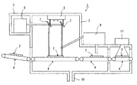
図1は、本発明の実施の形態に係るレジスト膜剥離除去装置1の一例を示す概略図である。レジスト膜剥離除去装置1は、レジスト膜除去の対象となるウェハ2を処理する処理チャンバ3と、ウェハ2を搬送するための複数のコンベア4と、処理チャンバ3横のレーザハウジング5内に収容されたレーザ手段6と、レーザ手段6からのレーザ光を反射させてウェハ2に照射させるガルバノミラー7と、ガルバノミラー7を駆動させるためのガルバノミラー駆動装置8と、レーザ照射前においては剥離のためレーザ照射後においては洗浄のためにウェハ2に水を供給する給水装置9と、処理チャンバ3に溜まった水を排出するための排水管10と、洗浄されたウェハ基板2を乾燥させるための乾燥装置11と、レーザ手段6、ガルバノミラー駆動装置8、乾燥装置11、コンベア4及び給水装置9をそれぞれ制御可能な制御装置(不図示)と、を備える。上記レーザ手段6は、所定波長、所定強度のレーザ光を、伝送経路内のガルバノミラー7を経由して、ウェハ基板2上のレジスト膜に照射する。レーザ手段6から出射された光は、ウェハ基板2と平行な方向に進み、ガルバノミラー7により略直角に曲げられウェハ基板2に照射される。ガルバノミラー7は、レーザ伝送経路に沿ってウェハ2の表面と平行な方向に移動可能である。また、レジスト膜剥離除去装置1は、ウェハ基板2に超音波振動を与える超音波洗浄手段をさらに備えていても良い。以下、本発明のレジスト膜剥離除去装置1の主な構成要素に関して詳細に説明する。
FIG. 1 is a schematic diagram showing an example of a resist film peeling and removing apparatus 1 according to an embodiment of the present invention. The resist film peeling / removing apparatus 1 is accommodated in a
〔レジスト膜の剥離に用いられる沸騰可能な液体〕
レジスト膜の剥離に用いられる沸騰・蒸発可能な液体は、レーザ手段6から照射されたレーザ光のSiウェハでのエネルギー吸収によりウェハ基板2とレジスト界面での熱応力に加えて、ウェハ基板に付着しているレジストと液体界面で液体自身の局所的な沸騰・蒸発によりウェハと液体を反対方向に押しのける力の反作用を利用してレジスト膜に衝撃を与えレジスト膜を剥離するためのものである。また、当該液体は、レーザ手段6から照射された光が当該液体を介してウェハ基板に吸収されなければならないため、レーザ手段6からの光を透過する液体であることが必要である。したがって、このようにSiウェハの加熱により沸騰・蒸発可能であってレーザ光を透過することができれば如何なる液体を使用しても良いが、当該液体は、水、水溶液或いは水分散液であることが好ましい。
[Boiling liquid used for resist film peeling]
The boilable / evaporable liquid used for removing the resist film adheres to the wafer substrate in addition to the thermal stress at the
レジスト膜剥離除去装置1に、上記沸騰・蒸発可能な液体の液体槽(容器)を設け、その中に浸漬した状態で上記レーザ光を照射してもよい。
〔基板〕
本発明は、ウェハ基板に代表されるレジスト膜が形成される広範囲の基板に対して有効であり、ウェハ基板を例に説明すれば、レーザ光がレジスト膜を透過してレジスト膜下のウェハ基板に吸収され、それによりウェハ基板が加熱され、ウェハ基板付近の液体が局所的に沸騰・蒸発し、沸騰・蒸発した液体がレジスト膜に衝撃を与えてウェハ基板からレジスト膜を剥離させるという原理に基づくものである。したがって、ウェハ基板としては、レーザ手段から照射された光を吸収するSi等の半導体基板が適用できる。本明細書において、基板の具体例としてウェハ基板を挙げているが、本発明に係る剥離作用を受けうる限り如何なる基板を用いてもよい。
The resist film peeling / removal apparatus 1 may be provided with a liquid tank (container) of the above boiling / evaporable liquid and irradiated with the laser beam in a state immersed in the liquid tank.
〔substrate〕
INDUSTRIAL APPLICABILITY The present invention is effective for a wide range of substrates on which a resist film typified by a wafer substrate is formed. If the wafer substrate is described as an example, the wafer substrate below the resist film through which the laser light passes through the resist film. The principle is that the wafer substrate is heated and the liquid in the vicinity of the wafer substrate is boiled and evaporated locally, and the boiled and evaporated liquid impacts the resist film and peels the resist film from the wafer substrate. Is based. Therefore, a semiconductor substrate such as Si that absorbs light irradiated from the laser means can be applied as the wafer substrate. In this specification, a wafer substrate is mentioned as a specific example of the substrate, but any substrate may be used as long as it can receive the peeling action according to the present invention.
〔レーザ手段〕
レーザ手段6は、レーザ光をウェハ基板2に照射することができ、これによりレジスト膜を当該ウェハ基板から剥離除去するものである。
[Laser means]
The laser means 6 can irradiate the
レーザ手段6として、如何なるレーザ手段を用いても良いが、単結晶のYAG、YVO4、YLF、YAlO3、GdVO4または多結晶セラミックのYAG、Y2O3、YVO4、YAlO3、GdVO4に、ドーパントとしてNd、Yb、Cr、Ti、Ho、Er、Tm、Taのうち1種または複数種添加されているものを媒質とする固体レーザ、若しくはArレーザ、Krレーザ、CO2レーザ等の気体レーザが挙げられる。レーザ手段6は、連続発振を行うレーザであっても良いし、またパルス発振を行うレーザであってもよい。レーザ手段6として特にNd:YAGレーザを用いることが好ましい。これは、大ビーム径、大出力のレーザ光線を発するものを安価に製造することができるからである。レジスト膜の局所を選択的に処理するために、ファイバーレーザーを使用すると良い場合がある。さらに、電気光変換効率が50%以上で経済的な半導体レーザを直接して使用する場合もある。 Any laser means may be used as the laser means 6, but single crystal YAG, YVO 4 , YLF, YAlO 3 , GdVO 4 or polycrystalline ceramic YAG, Y 2 O 3 , YVO 4 , YAlO 3 , GdVO 4 In addition, a solid laser or a Ar laser, a Kr laser, a CO 2 laser, or the like containing one or more of Nd, Yb, Cr, Ti, Ho, Er, Tm, and Ta as dopants is used as a medium. An example is a gas laser. The laser means 6 may be a laser that performs continuous oscillation or may be a laser that performs pulse oscillation. It is particularly preferable to use an Nd: YAG laser as the laser means 6. This is because a device that emits a laser beam having a large beam diameter and a large output can be manufactured at low cost. In some cases, a fiber laser may be used to selectively process the resist film. Furthermore, an economical semiconductor laser having an electro-optical conversion efficiency of 50% or more may be directly used.
レーザ手段6の発する光は、レジスト膜を透過することが必要である。ここで、光が透過するとは、その光の透過率が20%以上、好ましくは50%以上、更に好ましくは80〜100%の範囲にあることをいい、そのためには例えばレジスト膜としてノボラック系樹脂を使用した場合では、当該レジスト膜を透過する光の波長は300nm〜10.6μmの範囲にあり、500nm以上で80%以上の透過率が得られる。 The light emitted from the laser means 6 needs to pass through the resist film. Here, light transmission means that the light transmittance is in the range of 20% or more, preferably 50% or more, and more preferably in the range of 80 to 100%. For this purpose, for example, a novolak resin as a resist film is used. Is used, the wavelength of light transmitted through the resist film is in the range of 300 nm to 10.6 μm, and a transmittance of 80% or more is obtained at 500 nm or more.
また、レジスト膜を透過するレーザ光のパルス幅は、フェムト秒からミリ秒であることが好ましい。具体的には、当該パルス幅は、100フェムト秒〜500ミリ秒である。当該パルス幅がミリ秒を超えると液体の局所的な沸騰・蒸発が起こりにくくなりからであり、また照射する波長にもよるが100フェムト秒以下であると、照射される光の電界強度が大きくアブレーションによる除去が支配的となるためレジスト膜の剥離現象が生じないからである。 The pulse width of the laser light that passes through the resist film is preferably from femtoseconds to milliseconds. Specifically, the pulse width is 100 femtoseconds to 500 milliseconds. This is because when the pulse width exceeds milliseconds, local boiling / evaporation of the liquid is less likely to occur, and depending on the wavelength of irradiation, the electric field intensity of the irradiated light is large when the pulse width is 100 femtoseconds or less. This is because the stripping phenomenon of the resist film does not occur because the removal by ablation becomes dominant.
また、上記レジスト膜に照射されるレーザ光のエネルギー量が損傷閾値以下であることが好ましい。当該エネルギー量が損傷閾値以上であると、レーザ発振状態のばらつきにより部分的にSiウェハに損傷が生じる。より好ましくは、レーザ照射条件の影響によるレーザ損傷が完全に無視でき、多重照射が可能な50%以下である。 Moreover, it is preferable that the energy amount of the laser beam irradiated to the said resist film is below a damage threshold value. If the amount of energy is equal to or greater than the damage threshold, the Si wafer is partially damaged due to variations in the laser oscillation state. More preferably, the laser damage due to the influence of the laser irradiation condition can be completely ignored, and is 50% or less that allows multiple irradiation.
〔超音波洗浄手段〕
レジスト膜剥離除去装置1は、さらに超音波洗浄手段を備えていても良い。超音波洗浄手段は、下方に開放された有底筒状のケースを備え、このケース内の中心部に上下方向に振動する超音波振動子が配置され、この振動子の下側には下端をケースから突出させた棒状の振動伝達部材が配置されていてもよい。超音波振動子は上下一対のセラミック振動板の間に電極を挟んだもので、さらにその振動板の上下に振動伝達部材が重ねられてサンドイッチ状態にされ、これらはボルトで互いの層が強固に密着するように接合されている。こうしてセラミック振動板の振動が振動伝達部材に伝達されるようになっている。洗浄工程に付されたウェハ基板に超音波洗浄手段を直接接触させることにより振動を与えても良いし、ウェハ基板が浸漬された液体を介してウェハ基板に振動を与えても良い。また、コンベア4に当該超音波洗浄手段を当接させて振動を与えても良い。
[Ultrasonic cleaning means]
The resist film stripping / removing apparatus 1 may further include an ultrasonic cleaning unit. The ultrasonic cleaning means includes a bottomed cylindrical case that is opened downward, and an ultrasonic vibrator that vibrates in the vertical direction is disposed at the center of the case, and a lower end is provided below the vibrator. A rod-shaped vibration transmission member protruding from the case may be disposed. An ultrasonic vibrator is an electrode having an electrode sandwiched between a pair of upper and lower ceramic diaphragms. Further, a vibration transmitting member is stacked on the upper and lower parts of the diaphragm to form a sandwich, and these layers firmly adhere to each other with bolts. Are joined together. Thus, the vibration of the ceramic diaphragm is transmitted to the vibration transmitting member. Vibration may be applied by directly contacting the ultrasonic cleaning means with the wafer substrate subjected to the cleaning process, or vibration may be applied to the wafer substrate through a liquid in which the wafer substrate is immersed. Further, the ultrasonic cleaning means may be brought into contact with the
〔ガルバノミラー及びその駆動装置〕
以下に、ガルバノミラーについて詳細に説明する。ガルバノミラーとは、磁界中に配置された可動コイルに電流を流すことにより発生する回転トルクを利用したミラーであって、可動コイルと一体に回転する軸にミラーを設けて構成されるものである。このような構成のミラーは、微調整が可能であるため、正確にレーザ光をウェハ基板に照射することができる。また、ガルバノミラーを制御装置に接続することによりガルバノミラーの方向等を自動制御することができるため好適に用いられる。ガルバノミラーは、レーザハウジング5に収容されたレーザ手段6から照射されるレーザ光の進行方向に対して下方に45°傾斜した状態で、その進行方向に対して左右に首振り運動をすることができ、当該首振り運動により、レーザ光照射位置を、コンベア4の進行方向に対して垂直な方向に変位させることができる。
さらに、ガルバノミラーの駆動装置は、レーザ手段から水平方向に照射されるレーザ光の径路に沿ってガルバノミラーを移動させることができる。これらのガルバノミラー及びその駆動装置の可動手段により、レーザ手段から出射された光をウェハ基板の全ての領域に照射することができる。これらの可動手段はそれぞれ制御装置に接続され、それぞれ独立に駆動させることができる。
[Galvano mirror and its driving device]
The galvanometer mirror will be described in detail below. A galvano mirror is a mirror that uses rotational torque generated by passing a current through a movable coil arranged in a magnetic field, and is configured by providing a mirror on a shaft that rotates integrally with the movable coil. . Since the mirror having such a configuration can be finely adjusted, the laser beam can be accurately irradiated onto the wafer substrate. Further, it is preferably used because the direction of the galvanometer mirror can be automatically controlled by connecting the galvanometer mirror to the control device. The galvanometer mirror can swing to the left and right with respect to the traveling direction in a state where the galvanomirror is inclined 45 ° downward with respect to the traveling direction of the laser light emitted from the laser means 6 accommodated in the laser housing 5. The laser beam irradiation position can be displaced in a direction perpendicular to the traveling direction of the
Furthermore, the galvanometer mirror driving device can move the galvanometer mirror along the path of the laser beam irradiated in the horizontal direction from the laser means. With these galvanometer mirrors and the moving means of the driving device, the light emitted from the laser means can be irradiated to the entire area of the wafer substrate. Each of these movable means is connected to a control device and can be driven independently.
(レジスト膜剥離除去方法)
続いて、本発明に係るレジスト膜剥離除去方法を詳細に説明する。本発明は、レーザ光がレジスト膜を透過してレジスト膜下のウェハ基板に吸収され、それによりウェハ基板が加熱されて生じるレジストとSiウェハ界面での熱応力に加えて、ウェハ基板に付着しているレジストと液体界面で液体自身の局所的な沸騰・蒸発によりウェハと液体を反対方向に押しのける力の反作用を利用して、レジスト膜に衝撃を与えてウェハ基板から剥離させることに基づくものである。そのためこのような作用を受けうる限り、レジスト膜若しくはウェハ基板は如何なる材料により構成されていても良い。ここでは、レジスト膜としてノボラック系樹脂からなるレジストを、ウェハ基板としてSiウェハ基板を使用した場合について説明する。
(Resist film removal method)
Subsequently, the resist film peeling and removing method according to the present invention will be described in detail. In the present invention, laser light passes through the resist film and is absorbed by the wafer substrate under the resist film, and in addition to the thermal stress at the interface between the resist and the Si wafer generated by heating the wafer substrate, it adheres to the wafer substrate. Based on the reaction of the force that pushes the wafer and the liquid in the opposite directions by local boiling and evaporation of the liquid itself at the resist-liquid interface, the resist film is impacted and peeled off from the wafer substrate. is there. Therefore, the resist film or the wafer substrate may be made of any material as long as it can receive such an action. Here, a case where a resist made of a novolac resin is used as the resist film and a Si wafer substrate is used as the wafer substrate will be described.
1.浸漬工程
まず、レジスト膜除去に供されるレジスト膜等が形成されたウェハ基板を、レーザ光のエネルギーによる急激な膨張・拡散によりレジスト膜に衝撃を与えうる液体、例えば水に浸漬する。当該基板は上記液体に浸漬された状態であっても良いし、基板上に上記液体が塗布された状態にあってもよい。当該液体は、レジストとSiウェハ界面での熱応力に加えて、ウェハ基板に付着しているレジストと液体界面で液体自身の局所的な沸騰・蒸発によりウェハと液体を反対方向に押しのける力の反作用を利用して、レジスト膜に衝撃を与える限り如何なる液体でも良いが、環境負荷の観点からこの環境負荷の少ない水、純水を使用することが好ましい。しかし、上記の作用を発揮しうる限り、この水には他の有機物、無機物、イオン等が溶解していても良いし、水以外の他の液体、特に低沸点の液体であっても良い。
1. Immersion step First, a wafer substrate on which a resist film or the like to be used for resist film removal has been formed is immersed in a liquid, such as water, that can impact the resist film by rapid expansion / diffusion due to the energy of laser light. The substrate may be immersed in the liquid, or may be in a state where the liquid is applied on the substrate. In addition to the thermal stress at the resist-Si wafer interface, the liquid reacts with the force that pushes the wafer and liquid in the opposite direction by local boiling and evaporation of the liquid itself at the resist-liquid interface adhering to the wafer substrate. Any liquid may be used as long as it gives an impact on the resist film, but from the viewpoint of environmental load, it is preferable to use water or pure water having a low environmental load. However, as long as the above action can be exhibited, other organic substances, inorganic substances, ions, and the like may be dissolved in the water, or a liquid other than water, particularly a low boiling point liquid.
2.照射工程
続いて、レジスト膜がコートされたウェハ基板を例えば水に浸漬した状態で、又はウェハ基板上に形成されたレジスト膜上に水を塗布し、液体膜を形成した状態で、例えばNd:YAGレーザ手段からのレーザ光をレジスト膜を介してウェハ基板に照射する。ウェハ基板にレーザ光を照射することにより、ウェハ基板上のレジスト膜は部分的に剥離する。ここで、レジスト膜から水面までの距離は特に制限はない。レジスト膜から水面までの距離が大きくなるとエネルギーの損失により剥離できる面積が減少するが、その場合は照射するレーザ光のエネルギーを大きくすれば水面までの距離に関係なく照射ビーム径と同等の剥離面積が得られる。レーザ手段としては、光エネルギーが照射位置で上記剥離現象を生じ得る強度となるレーザ光を発振できればよく、固体レーザ、エキシマレーザ等の気体レーザ、あるいは半導体レーザなどレーザの発振形式を問わず、上記したようなレーザ手段を用いてもよい。
2. Irradiation Step Subsequently, in a state where the wafer substrate coated with the resist film is immersed in water, for example, or in a state where water is applied to the resist film formed on the wafer substrate to form a liquid film, for example, Nd: The wafer substrate is irradiated with laser light from the YAG laser means through a resist film. By irradiating the wafer substrate with laser light, the resist film on the wafer substrate is partially peeled off. Here, the distance from the resist film to the water surface is not particularly limited. As the distance from the resist film to the water surface increases, the area that can be removed decreases due to energy loss. In this case, if the energy of the irradiated laser beam is increased, the peeled area is equivalent to the irradiation beam diameter regardless of the distance to the water surface. Is obtained. The laser means only needs to be able to oscillate laser light whose intensity can cause the above peeling phenomenon at the irradiation position, regardless of the oscillation type of the laser such as a solid state laser, a gas laser such as an excimer laser, or a semiconductor laser. Such laser means may be used.
3.超音波洗浄工程
続いて、レジスト膜の一部が剥離されたウェハ基板を超音波洗浄工程に付し、上記照射工程では完全には除去されなかったレジスト膜を完全に取り除く。ここで、超音波発生手段は、ウェハ基板を浸漬する容器と物理的に連結されており、上記超音波発生手段を作用させることにより、容器及び該容器に満たされた水を介して、不完全に剥離されたレジスト膜に振動を与え、当該レジスト膜を完全に剥離させることができる。超音波発生手段は、上記レジスト膜に振動を与えることができる限り、如何なる部位に取り付けても良い。
本発明において、ウェハ基板上のレジスト膜を、レーザ光照射により沸騰・蒸発可能な液体で覆い、ウェハとレジスト界面での熱応力に加えて、ウェハ基板に付着しているレジストと液体界面で液体自身の局所的な沸騰・蒸発によりウェハと液体を反対方向に押しのける力の反作用を利用して、レジスト膜に衝撃を与えて剥離させるため、剥離したレジストは大きな破片として存在する。そのため、レーザ光を照射して処理された後の排水をろ過等することによりレジスト膜を回収することができる。
なお、上記液体膜は静止状態でも流動状態でもよく、剥離したレジストを除去回収するために液体膜を流動させるようにすることが便利な場合もある。
3. Ultrasonic Cleaning Process Subsequently, the wafer substrate from which a part of the resist film has been peeled is subjected to an ultrasonic cleaning process, and the resist film that was not completely removed in the irradiation process is completely removed. Here, the ultrasonic wave generation means is physically connected to the container in which the wafer substrate is immersed, and by operating the ultrasonic wave generation means, the container and the water filled in the container are imperfect. The resist film peeled off can be vibrated to completely peel off the resist film. The ultrasonic wave generation means may be attached to any part as long as vibration can be applied to the resist film.
In the present invention, the resist film on the wafer substrate is covered with a liquid that can be boiled / evaporated by laser light irradiation, and in addition to the thermal stress at the wafer / resist interface, the resist film attached to the wafer substrate is liquid at the interface. Since the resist film is impacted and peeled off by utilizing the reaction of the force that pushes the wafer and liquid in the opposite directions by their own local boiling and evaporation, the peeled resist exists as large pieces. Therefore, the resist film can be recovered by filtering the waste water after being irradiated with the laser beam.
The liquid film may be in a stationary state or a fluid state, and it may be convenient to make the liquid film flow in order to remove and recover the peeled resist.
(半導体装置の製造方法)
続いて、本発明に係るレジスト膜剥離除去方法を用いた半導体装置の製造方法について説明する。
まず、レジスト材料を溶媒に溶かしたレジスト膜形成用塗布液を半導体基板上に回転塗布しこれをベーキングすることによりレジスト膜を形成する。その後所望のようにパターン開口されたマスクを介してそのレジストに光、電子線などを照射しパターン転写する。そして、そのレジストを現像してレジストパターンを形成し、レジストパターンをエッチングマスクとして半導体基板をエッチングして加工する。その後、所望のようにエッチング加工された半導体基板を、上記と同様に例えば水に浸漬し、レジスト膜が水に浸漬された状態で、レーザ光をレジスト膜に照射する。レーザ光を照射することにより、半導体基板上のレジスト膜は部分的に剥離され、さらに超音波洗浄工程に付し、レジスト膜を完全に取り除くことで、所望のように加工され所定の機能を備える半導体装置を作製することができる。
(Method for manufacturing semiconductor device)
Then, the manufacturing method of the semiconductor device using the resist film peeling removal method concerning this invention is demonstrated.
First, a resist film forming coating solution in which a resist material is dissolved in a solvent is spin-coated on a semiconductor substrate and baked to form a resist film. Thereafter, the resist is irradiated with light, an electron beam or the like through a mask having a pattern opening as desired to transfer the pattern. Then, the resist is developed to form a resist pattern, and the semiconductor substrate is etched and processed using the resist pattern as an etching mask. Thereafter, the semiconductor substrate etched as desired is immersed in, for example, water in the same manner as described above, and the resist film is irradiated with laser light in a state where the resist film is immersed in water. By irradiating the laser beam, the resist film on the semiconductor substrate is partially peeled off, and further subjected to an ultrasonic cleaning process, and the resist film is completely removed to be processed as desired to have a predetermined function. A semiconductor device can be manufactured.
ノボラックレジストが塗布されたSiウェハ基板を純水を入れた水槽中に設置し、レジスト表面に対して垂直に、パルス幅5〜8nsのNd:YAGレーザーの基本波(1064nm)、第二高調波(532nm)、及び第三高調波(355nm)を焦点距離200mmのレンズを使用してそれぞれ単一照射した。レジストの有無はノマルスキー顕微鏡、及びXPSによる残留カーボン量の測定によって確認した。
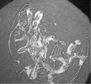
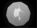
図2aは、ノボラックレジストを塗布したSiウェハを大気中に配置しこれに1064nm光を照射した場合のSiウェハ基板を示している。図2bは、図2aに示したSiウェハ基板の拡大図である。大気中においてノボラックレジストが塗布されたSiウェハ基板に1064nmのレーザ光を照射すると、レーザ光のエネルギー吸収により発生するウェハとレジスト界面での熱応力で僅かに剥離が生じたが、同時にSiウェハにも損傷が発生した。
図3aは、ノボラックレジストを塗布したSiウェハを大気中に配置しこれに532nm光を照射した場合のSiウェハ基板を示している。また、図3bは、図3aに示したSiウェハ基板の拡大図である。532nmのレーザ光を照射した場合も1064nm光を照射した場合と同様、レジスト剥離とウェハ損傷が同時に起こった。
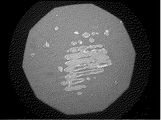
図2cは、本発明に係るレジスト膜剥離除去方法を用い、1064nmのレーザ光が照射されたSiウェハ基板の表面を示している。さらに、図3cは、本発明に係るレジスト膜剥離除去方法を用い、532nmのレーザ光が照射されたSiウェハ基板の表面を示している。図2c及び図3cに示すように、本発明に係る方法によれば、Si基板に損傷を与えることなく、レジスト膜を除去することができた。これは、水中においてレーザ光を照射するため、レジストとSiウェハ界面での熱応力に加えて、ウェハ基板に付着しているレジストと液体界面で液体自身の局所的な沸騰・蒸発によりウェハと液体を反対方向に押しのける力の反作用を利用してレーザ光からの光を効率よく用いることができ、それによりレーザ光の強度を抑えることができるためである。XPSの残留カーボン量の測定でもレジストの剥離を確認することができた。
続いて、レジスト表面からの純水の深さを5、10mmと変えて、532nm光をノボラックレジストを塗布したSiウェハ基板にそれぞれ照射した。図4は、当該深さを5mmとし、図5は当該深さを10mmとして532nm光を照射した場合のSiウェハ基板の表面を示している。
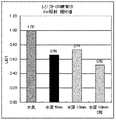
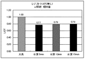
大気中に設置して照射したときのレジスト剥離とウェハの損傷がほぼ同時に起こるレーザーエネルギーの閾値を1とした場合、深さが5mmの場合は約30%、10mmでも約30%それぞれ低減することができた(図6)。さらに50%低減させたレーザーエネルギーでは、同一箇所に2発照射すれば剥離できることが分かった(図6)。これは、多重照射すればレーザーエネルギーを大幅に低減できることを示している。このように、レジストとSiウェハ界面での熱応力に加えて、ウェハ基板に付着しているレジストと液体界面で液体自身の局所的な沸騰・蒸発によりウェハと液体を反対方向に押しのける力の反作用を利用すれば、剥離に必要なレーザーエネルギーを大幅に低減でき、Siウェハに損傷を発生させずに従来では困難であった剥離が可能となった。
また、レジスト表面からの純水の深さを5、10mm、15mmと変えて、1064nm光をノボラックレジストを塗布したSiウェハにそれぞれ照射した。図7は、当該深さを5mmとし、図8は当該深さを10mmとして1064nm光を照射した場合のSiウェハ基板の表面を示している。
大気中に設置して照射したときのレジスト剥離とウェハの損傷がほぼ同時に起こるレーザーエネルギーの閾値を1とした場合、深さが5mmの場合は約20%、10mmで約20%、15mmでも20%それぞれ低減することができた(図9)。532nm光の結果と同様に、本発明ではフォトンコストが極めて安価な1064nm光でもSiウェハに損傷を発生させずに従来では困難であった剥離が可能となった。
続いて、水深による剥離状況の違いについて検討した。0.5J/cm2の1064nm光を純水の深さ5、10mmでノボラックレジストを塗布したSiウェハにそれぞれ照射した場合、水深が深くなるほど剥離される領域が低減した。48.4mJ/cm2の532nm光を同様に照射した場合も同様の結果が得られることが分かった。しかしながら、水深が深い場合はレーザ光の強度を大きくすれば剥離面積の増加は実現できることから、剥離メカニズムについては水深による影響は無いと考えられる。
続いて、超音波洗浄の効果について検討した。ノボラックレジストを塗布したSiウェハにレーザ光を照射した場合、レーザ光のビームパターンによっては剥離できていない部分も存在する場合もある(図10)。そこで、超音波洗浄機(周波数28kHz、出力60W)を用いて同じ純水中で処理したところ、完全に剥離できていなかった部分をきれいに剥離させることができた(図11)。また剥離したレジストは破片で存在するために、洗浄工程において回収できる。このように、超音波洗浄など物理的にウェハとレジストを振動させる機構を組み合わせれば、剥離のレーザーエネルギーを低減でき、さらに局所的に剥離が不完全な部分も除去が可能となる。
A Si wafer substrate coated with a novolak resist is placed in a water tank containing pure water, and a Nd: YAG laser fundamental wave (1064 nm) and second harmonic wave with a pulse width of 5 to 8 ns perpendicular to the resist surface. (532 nm) and third harmonic (355 nm) were each irradiated with a single lens using a focal length of 200 mm. The presence or absence of the resist was confirmed by measuring the amount of residual carbon with a Nomarski microscope and XPS.
FIG. 2a shows a Si wafer substrate when a Si wafer coated with a novolak resist is placed in the atmosphere and irradiated with 1064 nm light. FIG. 2b is an enlarged view of the Si wafer substrate shown in FIG. 2a. When a 1064 nm laser beam was irradiated to a Si wafer substrate coated with a novolak resist in the atmosphere, a slight peeling occurred due to thermal stress at the wafer-resist interface caused by energy absorption of the laser beam. Even damage occurred.
FIG. 3a shows a Si wafer substrate when a Si wafer coated with a novolak resist is placed in the atmosphere and irradiated with 532 nm light. FIG. 3b is an enlarged view of the Si wafer substrate shown in FIG. 3a. In the case of irradiation with 532 nm laser light, resist peeling and wafer damage occurred simultaneously as in the case of irradiation with 1064 nm light.
FIG. 2c shows the surface of a Si wafer substrate irradiated with a 1064 nm laser beam using the resist film peeling and removing method according to the present invention. Further, FIG. 3c shows the surface of a Si wafer substrate irradiated with a laser beam of 532 nm using the resist film peeling and removing method according to the present invention. As shown in FIGS. 2c and 3c, according to the method of the present invention, the resist film could be removed without damaging the Si substrate. In order to irradiate laser light in water, in addition to the thermal stress at the resist and Si wafer interface, the wafer and liquid are locally boiled and evaporated at the resist and liquid interface adhering to the wafer substrate. This is because the light from the laser beam can be used efficiently by utilizing the reaction of the force that pushes the lens in the opposite direction, thereby suppressing the intensity of the laser beam. The resist peeling could also be confirmed by measuring the amount of residual carbon in XPS.
Subsequently, the depth of pure water from the resist surface was changed to 5 and 10 mm, and each of the Si wafer substrates coated with the novolak resist was irradiated with 532 nm light. FIG. 4 shows the surface of the Si wafer substrate when the depth is 5 mm and FIG. 5 is irradiated with 532 nm light with the depth being 10 mm.
When the threshold value of laser energy at which resist peeling and wafer damage occur almost simultaneously when installed in the atmosphere is set to 1, the depth is reduced by approximately 30% when the depth is 5 mm and approximately 30% even when 10 mm. (Fig. 6). Further, it was found that the laser energy reduced by 50% can be peeled off if the same spot is irradiated twice (FIG. 6). This indicates that laser energy can be greatly reduced by multiple irradiation. In this way, in addition to the thermal stress at the resist / Si wafer interface, the reaction of the force that pushes the wafer and liquid in the opposite directions by local boiling / evaporation of the liquid itself at the resist / liquid interface adhering to the wafer substrate. By using this, the laser energy required for peeling can be greatly reduced, and peeling that has been difficult in the past can be performed without causing damage to the Si wafer.
Further, the depth of pure water from the resist surface was changed to 5, 10 mm, and 15 mm, and 1064 nm light was irradiated to the Si wafer coated with the novolak resist. FIG. 7 shows the surface of the Si wafer substrate when the depth is 5 mm and FIG. 8 is irradiated with 1064 nm light with the depth being 10 mm.
When the threshold of laser energy at which resist peeling and wafer damage occur almost simultaneously when installed in the atmosphere is assumed to be 1, when the depth is 5 mm, it is about 20%, 10 mm is about 20%, and 15 mm is 20%. % Can be reduced respectively (FIG. 9). Similar to the result of 532 nm light, in the present invention, even with 1064 nm light, which has a very low photon cost, the Si wafer can be peeled off without causing damage to the Si wafer.
Then, the difference in the peeling situation by the water depth was examined. When 1064 nm light of 0.5 J / cm 2 was applied to each Si wafer coated with novolak resist at a depth of 5 or 10 mm of pure water, the peeled area decreased as the water depth increased. It was found that the same result was obtained when 532 nm light of 48.4 mJ / cm 2 was similarly irradiated. However, when the water depth is deep, an increase in the peeled area can be realized by increasing the intensity of the laser beam. Therefore, it is considered that the peeling mechanism has no influence due to the water depth.
Subsequently, the effect of ultrasonic cleaning was examined. When a Si wafer coated with a novolak resist is irradiated with laser light, there may be a portion that cannot be removed depending on the beam pattern of the laser light (FIG. 10). Then, when it processed in the same pure water using the ultrasonic cleaner (frequency 28kHz, output 60W), the part which was not able to be peeled completely was able to be peeled cleanly (FIG. 11). Further, since the peeled resist exists as fragments, it can be recovered in the cleaning process. In this manner, by combining a mechanism that physically vibrates the wafer and the resist, such as ultrasonic cleaning, it is possible to reduce the laser energy for peeling, and it is also possible to remove locally incompletely peeled portions.
なお、照射波長が355nmでは、レジストへ透過率は約40%程度ある。そのため、レジストとSiウェハ界面での熱応力による極めて僅かな剥離に加えて、フォトンエネルギーも高いことからアブレーションによる除去の両方が生じる。しかしながら、照射するフォトエネルギーが大きいことからアブレーションによる除去が支配的となり、図13a及び図13bに示すように、Siウエハーへの損傷を与えずにレジストを除去することができる。以上のようにSiウェハ上に塗布されたノボラックレジストでは、レジストの透過率、照射波長のフォトンエネルギーからパルス幅ナノ秒の355nmではアブレーションによる除去が支配的であるが、本発明で重要なレジストとSiウェハ界面での熱応力による極めて僅かな剥離現象が生じる領域ともなる。 When the irradiation wavelength is 355 nm, the transmittance to the resist is about 40%. Therefore, in addition to extremely slight peeling due to thermal stress at the interface between the resist and the Si wafer, both the removal by ablation occurs because the photon energy is high. However, since the photo energy to be irradiated is large, removal by ablation becomes dominant, and the resist can be removed without damaging the Si wafer, as shown in FIGS. 13a and 13b. As described above, in the novolak resist applied on the Si wafer, the removal by ablation is dominant at 355 nm of pulse width nanosecond from the transmittance of the resist and the photon energy of the irradiation wavelength. It is also a region where a very slight peeling phenomenon occurs due to thermal stress at the Si wafer interface.
Claims (28)
The resist film peeling and removing method according to claim 13, wherein the temperature of the liquid film formed on the resist film is set higher or lower than the normal liquid temperature.
21. The semiconductor manufacturing apparatus including a resist film stripping / removing facility according to claim 20, further comprising means for recovering a stripped resist film that is separated from the cleaning liquid and substantially free of ablation.
Priority Applications (1)
| Application Number | Priority Date | Filing Date | Title |
|---|---|---|---|
| JP2006215979A JP2008042017A (en) | 2006-08-08 | 2006-08-08 | Resist peeling and removing method capable of recovering resist and semiconductor manufacturing device using it |
Applications Claiming Priority (1)
| Application Number | Priority Date | Filing Date | Title |
|---|---|---|---|
| JP2006215979A JP2008042017A (en) | 2006-08-08 | 2006-08-08 | Resist peeling and removing method capable of recovering resist and semiconductor manufacturing device using it |
Publications (2)
| Publication Number | Publication Date |
|---|---|
| JP2008042017A true JP2008042017A (en) | 2008-02-21 |
| JP2008042017A5 JP2008042017A5 (en) | 2009-09-17 |
Family
ID=39176681
Family Applications (1)
| Application Number | Title | Priority Date | Filing Date |
|---|---|---|---|
| JP2006215979A Pending JP2008042017A (en) | 2006-08-08 | 2006-08-08 | Resist peeling and removing method capable of recovering resist and semiconductor manufacturing device using it |
Country Status (1)
| Country | Link |
|---|---|
| JP (1) | JP2008042017A (en) |
Cited By (4)
| Publication number | Priority date | Publication date | Assignee | Title |
|---|---|---|---|---|
| KR101607706B1 (en) | 2008-06-13 | 2016-03-30 | 예놉틱 아우토마티지어룽스테히닉 게엠베하 | Recycling process for thin film solar cell modules |
| CN106797014A (en) * | 2014-09-12 | 2017-05-31 | 东莞新能源科技有限公司 | The removal device of pole piece coating |
| CN106797015A (en) * | 2014-09-12 | 2017-05-31 | 东莞新能源科技有限公司 | The removing method of pole piece coating |
| CN109570151A (en) * | 2019-01-25 | 2019-04-05 | 中国工程物理研究院激光聚变研究中心 | The device and cleaning method of liquid stream ULTRASONIC COMPLEX auxiliary laser cleaning optical element |
Citations (5)
| Publication number | Priority date | Publication date | Assignee | Title |
|---|---|---|---|---|
| JPH11145108A (en) * | 1997-11-05 | 1999-05-28 | Denso Corp | Method and device of fine work device |
| JP2003249427A (en) * | 2001-12-17 | 2003-09-05 | Tokyo Electron Ltd | Film removing apparatus and method |
| JP2003303789A (en) * | 2002-04-10 | 2003-10-24 | Laser Gijutsu Sogo Kenkyusho | Method and equipment for exfoliating photoresist |
| JP2004157424A (en) * | 2002-11-08 | 2004-06-03 | Sony Corp | Method for stripping resist and method for manufacturing semiconductor device |
| JP2005340668A (en) * | 2004-05-28 | 2005-12-08 | Purex:Kk | Method and apparatus for removing organic substance |
-
2006
- 2006-08-08 JP JP2006215979A patent/JP2008042017A/en active Pending
Patent Citations (5)
| Publication number | Priority date | Publication date | Assignee | Title |
|---|---|---|---|---|
| JPH11145108A (en) * | 1997-11-05 | 1999-05-28 | Denso Corp | Method and device of fine work device |
| JP2003249427A (en) * | 2001-12-17 | 2003-09-05 | Tokyo Electron Ltd | Film removing apparatus and method |
| JP2003303789A (en) * | 2002-04-10 | 2003-10-24 | Laser Gijutsu Sogo Kenkyusho | Method and equipment for exfoliating photoresist |
| JP2004157424A (en) * | 2002-11-08 | 2004-06-03 | Sony Corp | Method for stripping resist and method for manufacturing semiconductor device |
| JP2005340668A (en) * | 2004-05-28 | 2005-12-08 | Purex:Kk | Method and apparatus for removing organic substance |
Cited By (6)
| Publication number | Priority date | Publication date | Assignee | Title |
|---|---|---|---|---|
| KR101607706B1 (en) | 2008-06-13 | 2016-03-30 | 예놉틱 아우토마티지어룽스테히닉 게엠베하 | Recycling process for thin film solar cell modules |
| CN106797014A (en) * | 2014-09-12 | 2017-05-31 | 东莞新能源科技有限公司 | The removal device of pole piece coating |
| CN106797015A (en) * | 2014-09-12 | 2017-05-31 | 东莞新能源科技有限公司 | The removing method of pole piece coating |
| EP3190646A4 (en) * | 2014-09-12 | 2018-04-04 | Dongguan Amperex Technology Limited | Electrode plate coating removal method |
| CN109570151A (en) * | 2019-01-25 | 2019-04-05 | 中国工程物理研究院激光聚变研究中心 | The device and cleaning method of liquid stream ULTRASONIC COMPLEX auxiliary laser cleaning optical element |
| CN109570151B (en) * | 2019-01-25 | 2023-12-22 | 中国工程物理研究院激光聚变研究中心 | Device and method for cleaning optical element by liquid flow ultrasonic composite auxiliary laser |
Similar Documents
| Publication | Publication Date | Title |
|---|---|---|
| JP4861609B2 (en) | Method and apparatus for removing organic substances | |
| JP5816409B2 (en) | Method to increase throughput for laser via drilling | |
| JP2006229198A (en) | Method and apparatus for cleaning tool with ultraviolet provided internally | |
| TWI673764B (en) | Sacrificial layer for post-laser debris removal systems and methods | |
| US6933464B2 (en) | Laser-driven cleaning using reactive gases | |
| KR20060054058A (en) | Method, treatment liquid and apparatus for removing adhesive material from substrate surface | |
| JP2003133690A (en) | Method for forming circuit by using ultra short pulse laser | |
| JP2008042017A (en) | Resist peeling and removing method capable of recovering resist and semiconductor manufacturing device using it | |
| JP2010045283A (en) | Contamination removal device, contamination removal method and pattern substrate manufacturing method | |
| JP4247383B2 (en) | Fine ablation processing method of transparent material | |
| TWI330765B (en) | Photoresist peeling/removing method and device | |
| JPH10116809A (en) | Method and system for washing | |
| JP2008242175A (en) | Forming method of thin film pattern and manufacturing method of black matrix substrate for color filter | |
| JP2007012733A (en) | Dividing method of substrate | |
| JP2008042017A5 (en) | ||
| JP4883975B2 (en) | Method for removing deposits on substrate surface, treatment liquid for removal and removal apparatus | |
| JP3998974B2 (en) | Circuit board patterning method | |
| JP3106040B2 (en) | Dry cleaning system for substrate surface | |
| JP2000202664A (en) | Lasder drilling method | |
| RU2764237C1 (en) | Method and device for cleaning substrate and computer software product | |
| JP2003285183A (en) | Laser beam machining device and machining method | |
| KR100589673B1 (en) | Washing Methods based on pulse laser-induced shock wave and evaporation of liquid film and Apparatus thereof | |
| JP2004157424A (en) | Method for stripping resist and method for manufacturing semiconductor device | |
| KR20040044317A (en) | Method and apparatus of descaling metal using pulse laser-induced shock wave | |
| JP2002373878A (en) | Apparatus and method of cleaning substrate surface |
Legal Events
| Date | Code | Title | Description |
|---|---|---|---|
| RD03 | Notification of appointment of power of attorney |
Effective date: 20080214 Free format text: JAPANESE INTERMEDIATE CODE: A7423 |
|
| A521 | Written amendment |
Free format text: JAPANESE INTERMEDIATE CODE: A821 Effective date: 20080214 |
|
| A521 | Written amendment |
Effective date: 20090805 Free format text: JAPANESE INTERMEDIATE CODE: A523 |
|
| A621 | Written request for application examination |
Free format text: JAPANESE INTERMEDIATE CODE: A621 Effective date: 20090805 |
|
| A131 | Notification of reasons for refusal |
Effective date: 20110816 Free format text: JAPANESE INTERMEDIATE CODE: A131 |
|
| A02 | Decision of refusal |
Free format text: JAPANESE INTERMEDIATE CODE: A02 Effective date: 20111227 |