JP2008032702A - Defect inspecting device and method - Google Patents
Defect inspecting device and method Download PDFInfo
- Publication number
- JP2008032702A JP2008032702A JP2007175160A JP2007175160A JP2008032702A JP 2008032702 A JP2008032702 A JP 2008032702A JP 2007175160 A JP2007175160 A JP 2007175160A JP 2007175160 A JP2007175160 A JP 2007175160A JP 2008032702 A JP2008032702 A JP 2008032702A
- Authority
- JP
- Japan
- Prior art keywords
- defect
- inspection
- defect information
- substrate
- information
- Prior art date
- Legal status (The legal status is an assumption and is not a legal conclusion. Google has not performed a legal analysis and makes no representation as to the accuracy of the status listed.)
- Pending
Links
Images


Landscapes
- Investigating Materials By The Use Of Optical Means Adapted For Particular Applications (AREA)
- Exposure And Positioning Against Photoresist Photosensitive Materials (AREA)
Abstract
Description
本発明は、被検査対象物の外観を検査して欠陥を検出する欠陥検査装置および欠陥検査方法に関する。 The present invention relates to a defect inspection apparatus and a defect inspection method for detecting defects by inspecting the appearance of an object to be inspected.
液晶表示用のマザーガラス基板(ワーク)を製造する(フォトリソグラフィ)製造工程においては、ワーク上に薄膜の形成等が行われた後、ワークの表面のキズ、ゴミ付着、回路パターン不良などの欠陥検査が行われている。この欠陥検査において、欠陥検査装置にワークが搬入されると、欠陥検査装置は、画像処理等によって、ワーク上の欠陥を検出し、その欠陥を識別するための欠陥位置等の情報を含む欠陥情報を生成する。この欠陥情報はサーバへ送信され、他の検査装置によって生成された欠陥情報と共に、サーバによって一括して管理される。 In the manufacturing process of manufacturing a mother glass substrate (work) for liquid crystal display (photolithography), defects such as scratches on the surface of the work, adhesion of dust, circuit pattern defects, etc., after a thin film is formed on the work Inspection is being conducted. In this defect inspection, when a work is brought into the defect inspection apparatus, the defect inspection apparatus detects defect on the work by image processing or the like, and includes defect information including information such as a defect position for identifying the defect. Is generated. This defect information is transmitted to the server, and is collectively managed by the server together with the defect information generated by another inspection apparatus.
従来の欠陥検査装置は、欠陥情報に基づいて欠陥の大きさや欠陥の位置および欠陥の個数により、修正(リペア)する基板か、リワークする基板か、廃棄する基板か、ワークの品質を判定し、判定結果に基づいてワークの搬出先を決定していた。例えば、ワーク上の欠陥が次工程に影響を与えない擬似欠陥である場合には、次工程の製造装置へのワークの搬出が決定され、修正不可能な欠陥である場合には、ワークの廃棄が決定され、欠陥の修正が可能な場合には、欠陥修正装置へのワークの搬出が決定される。 A conventional defect inspection apparatus determines the quality of a work, whether it is a substrate to be repaired, a substrate to be reworked, a substrate to be discarded, or a substrate to be discarded, according to the size of the defect, the position of the defect, and the number of defects based on the defect information. The work delivery destination was determined based on the determination result. For example, when a defect on the workpiece is a pseudo defect that does not affect the next process, it is determined that the workpiece is carried out to the manufacturing apparatus for the next process, and when it is an uncorrectable defect, the workpiece is discarded. When the defect can be corrected, it is determined to carry out the work to the defect correcting device.
検査装置による欠陥の検出結果を用いる従来技術には、例えば以下のようなものがある。特許文献1には、第1の検査装置で液晶基板の検査を行った後、さらに第2の検査装置で検査を行い、それらの検査の際に生じた検査データに基づいて、液晶基板の品質の判定およびロットへの振り分けを決定することによって、品質の判定および振り分けにおける人為的なミスを防止し、精度の高い液晶基板の選別を行うことが記載されている。 Examples of conventional techniques that use the detection results of defects by an inspection apparatus include the following. In Patent Document 1, after the liquid crystal substrate is inspected by the first inspection apparatus, the inspection is further performed by the second inspection apparatus, and the quality of the liquid crystal substrate is determined based on the inspection data generated during the inspection. It is described that the determination of quality and the allocation to lots are determined to prevent human error in quality determination and allocation and to select a liquid crystal substrate with high accuracy.
また、特許文献2には、現在モニタ中の検査装置の検査データを表示する画面上に他の複数の検査装置のうちの任意の検査データを同時に表示すると共に、他の検査装置によって検出された不良数と、現在モニタ中の検査装置によって検出された不良数との比である不良捕捉率を求め、不良捕捉率に応じて、モニタ中の検査装置の感度を調節することによって、モニタ中の検査装置の感度を一定水準に保つことが記載されている。
従来各工程で、検査装置によりワークの品質が判定されると、そのワークの搬出先は、現時点の欠陥情報に基づいて決定されている。例えば、製造装置により処理されたワークは、検査装置によって検出された欠陥情報に基づいて搬出先が判断されている。このとき、液晶表示用のマザーガラス基板に形成されているレイヤーは、きわめて薄いために、前工程の下層レイヤーに発生した擬似欠陥が最上層のレイヤーを透過し、重複して検出される場合がある。例えばオートマクロ検査装置では、修正が必要であると判断された欠陥が、ミクロ検査装置による詳細検査により修正不要の擬似欠陥と判断される場合がある。 Conventionally, when the quality of a workpiece is determined by an inspection apparatus in each process, the unloading destination of the workpiece is determined based on the current defect information. For example, the work destination processed by the manufacturing apparatus is determined as a delivery destination based on defect information detected by the inspection apparatus. At this time, since the layer formed on the mother glass substrate for liquid crystal display is extremely thin, the pseudo defects generated in the lower layer in the previous process may pass through the uppermost layer and may be detected redundantly. is there. For example, in an auto macro inspection apparatus, a defect determined to be corrected may be determined as a pseudo defect that does not require correction by a detailed inspection by a micro inspection apparatus.
この下層レイヤーの欠陥は、前工程で次工程へ影響を与えない問題のない欠陥として判断されたものである。したがって、検査装置は、下層レイヤーの欠陥を重複して検出した場合、この下層の欠陥を修正が必要であると誤判断し、このワークを欠陥修正装置へ搬送する場合がある。また、オートマクロ検査装置で検出された各欠陥は、ミクロ検査装置によって拡大視され、修正が不要な欠陥と修正が必要な欠陥に判別される。このレビュー検査は、オートマクロ検査装置で検出された各欠陥の位置情報に基づいて顕微鏡の対物レンズを移動させ、各欠陥を詳細に観察している。オートマクロ検査装置は、下層レイヤー欠陥と上層レイヤー欠陥とを判別できないため、レビュー検査では全欠陥を観察することになる。 This defect in the lower layer is determined as a defect that does not affect the next process in the previous process. Accordingly, when the inspection apparatus detects a defect in the lower layer in an overlapping manner, the inspection apparatus may erroneously determine that the defect in the lower layer needs to be corrected and transport the work to the defect correction apparatus. Further, each defect detected by the auto macro inspection apparatus is magnified by the micro inspection apparatus, and is determined as a defect that does not need to be corrected and a defect that requires correction. In this review inspection, the objective lens of the microscope is moved based on the position information of each defect detected by the auto macro inspection apparatus, and each defect is observed in detail. Since the auto macro inspection apparatus cannot distinguish between the lower layer defect and the upper layer defect, all the defects are observed in the review inspection.
このように、従来においては、下層欠陥を含む欠陥情報に基づいて、ワークの搬出先(行き先)が決定される結果、適切な搬出先にワークが搬出されないことがある。このような場合には、搬送用のカセットに対するワークの出し入れの時間や搬送時間が無駄となり、レビュー検査時には重複して欠陥を検査することになるので、製造工程に掛かるリードタイムを短縮することができないという問題がある。 As described above, in the related art, as a result of determining the work delivery destination (destination) based on the defect information including the lower layer defect, the work may not be delivered to an appropriate delivery destination. In such a case, the time for loading and unloading the workpiece with respect to the cassette for conveyance and the conveyance time are wasted, and the defect is inspected repeatedly at the time of review inspection, so the lead time for the manufacturing process can be shortened. There is a problem that you can not.
本発明は、上述した問題点に鑑みてなされたものであって、製造工程のリードタイムを短縮することができる欠陥検査装置および欠陥検査方法を提供することを目的とする。 The present invention has been made in view of the above-described problems, and an object of the present invention is to provide a defect inspection apparatus and a defect inspection method that can shorten the lead time of a manufacturing process.
本発明は、上記の課題を解決するためになされたもので、レイヤーの製造工程毎に基板上の欠陥を検査し、前記欠陥を識別する欠陥情報を生成する欠陥検査装置に関する。この欠陥検査装置は、最上層レイヤーの検査時に生成された前記基板の前記欠陥情報と、前記基板の下層レイヤーの検査時に生成された前記基板の前記欠陥情報とを比較し、前記下層レイヤーが欠陥と重複する重複欠陥を除いて前記最上層レイヤー上に発生した欠陥を識別する注目欠陥情報を生成する情報生成手段と、前記注目欠陥情報に基づいて、前記基板の搬出先を判断する判断手段とを備える。 The present invention has been made to solve the above problems, and relates to a defect inspection apparatus that inspects a defect on a substrate for each layer manufacturing process and generates defect information for identifying the defect. The defect inspection apparatus compares the defect information of the substrate generated during the inspection of the uppermost layer with the defect information of the substrate generated during the inspection of the lower layer of the substrate, and the lower layer is defective. And information generating means for generating attention defect information for identifying defects generated on the uppermost layer except for overlapping defects that overlap with each other, and determination means for determining the substrate delivery destination based on the attention defect information Is provided.
また、本発明は、レイヤーの製造工程毎に基板上の欠陥を検査し、前記欠陥を識別する欠陥情報を生成する欠陥検査方法に関する。この欠陥検査方法は、最上層レイヤー検査時に生成された前記基板の前記欠陥情報と、前記基板の下層レイヤーの検査時に生成された前記基板の前記欠陥情報とを比較して、前記下層レイヤーの欠陥と重複する重複欠陥を除いて、前記最上層レイヤー上に発生した欠陥を識別する注目欠陥情報を生成する第1のステップと、前記注目欠陥情報に基づいて、前記基板の搬出先を判断する第2のステップとを備える。 The present invention also relates to a defect inspection method for inspecting a defect on a substrate for each layer manufacturing process and generating defect information for identifying the defect. The defect inspection method compares the defect information of the substrate generated at the time of inspection of the uppermost layer with the defect information of the substrate generated at the time of inspection of the lower layer of the substrate. A first step of generating attention defect information for identifying a defect generated on the uppermost layer, excluding overlapping defects that overlap with the first defect, and determining a carry-out destination of the substrate based on the attention defect information. 2 steps.
本発明によれば、製造工程のリードタイムを短縮することができるという効果が得られる。 According to the present invention, it is possible to reduce the lead time of the manufacturing process.
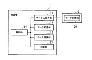
以下、図面を参照し、本発明を実施するための最良の形態について説明する。図1は、本発明の第1の実施形態による欠陥検査装置の構成を示すブロック図である。以下、図中の各構成について説明する。検査機1は、例えば、半導体ウエハ基板や液晶表示用ガラス基板などフォトリソグラフィプロセスにより、表面に複数のレイヤーを順次積層して製造される複検体をマクロ検査あるいはミクロ検査をして、欠陥を検出する欠陥検査装置である。外部装置2は、検査時に生成された欠陥情報等を記憶するデータ記憶部20を備えたサーバ等である。欠陥情報には、欠陥の位置(座標)を示す欠陥位置情報や、欠陥の種別を示す欠陥種別情報等が含まれている。検査機1と外部装置2は、ネットワークあるいは専用回線を介して接続されている。検査機1の検査部によって検出された被検体の欠陥情報はデータ記憶部20に格納される。
The best mode for carrying out the present invention will be described below with reference to the drawings. FIG. 1 is a block diagram showing the configuration of the defect inspection apparatus according to the first embodiment of the present invention. Hereinafter, each component in the figure will be described. The inspection machine 1 detects a defect by performing a macro inspection or a micro inspection on a plurality of samples manufactured by sequentially laminating a plurality of layers on a surface by a photolithography process such as a semiconductor wafer substrate or a liquid crystal display glass substrate. It is a defect inspection device. The
検査機1において、データ入出力部10は外部装置2と通信を行う。データ記憶部11は、検査機1の検査部によって検出された各工程毎の欠陥情報や、データ入出力部10を介して入力された他の欠陥検査装置の欠陥情報、検査機1によって行われる処理の手順や設定条件等を示すレシピ情報等を記憶する。データ演算部12は、欠陥情報を用いて、新規な欠陥を抽出する演算を行う。判断部13は、データ演算部12による演算の結果に基づいて、検査機1に搬入されたワークの搬出先を判断する。制御部14は検査機1の各部の動作を制御する他、欠陥情報の生成等を行う。なお、ワークの欠陥検査を行う検査部や、各種の情報を表示する表示部、ユーザによって操作される操作部等の構成の図示は省略されている。
In the inspection machine 1, the data input /
次に、データ演算部12が行う演算を説明する。データ演算部12は、検査機1の検査部において検査が行われた後、その検査時に生成された最上層の欠陥情報(第1の欠陥情報とする)と、その検査よりも以前の製造工程で行われた検査時に生成された下層の欠陥情報(第2の欠陥情報とする)とを用いて演算を行い、現製造工程において最上層に発生した新規な欠陥を識別する注目欠陥情報を生成する。例えば、検査機1はマクロ検査装置とする。また、第1の欠陥情報は、検査対象となる基板が検査機1に搬入された現製造工程検査時(レイヤーNの検査とする)に、検査機1によって生成された情報とする。また、第2の欠陥情報は、その現製造工程(レイヤーNが形成される工程)よりも1つ前の製造工程検査時(レイヤーN−1の検査とする)に、検査機1によって生成された同じワークの下層欠陥情報とする。レイヤーとは、ワーク上に形成される被膜を識別するための用語であり、ワーク上に形成された順番にレイヤー1、レイヤー2、・・・というように識別されるとする。この基板の最上層のレイヤーNは、現製造工程で形成されたものとし、その直下のレイヤーN−1は、1つ前の製造工程で形成されたものとする。
Next, the calculation performed by the
データ演算部12は、第1の欠陥情報によって示される欠陥から、第2の欠陥情報によって示される欠陥を除き、残った欠陥の情報を最上層の注目欠陥情報とする。より具体的には、データ演算部12は、第1の欠陥情報に含まれる欠陥位置情報と、第2の欠陥情報に含まれる欠陥位置情報とを比較し、第1の欠陥情報から第2の欠陥情報を除いた欠陥が最上層に発生した新規な欠陥であると判断する。例えば、データ演算部12は、第1の欠陥情報から欠陥点を1つ選択し、その欠陥点と同一の欠陥点が第2の欠陥情報に含まれているか否かを判断する。
The
例えば、データ演算部12は第2の欠陥情報からも欠陥点を1つ選択し、欠陥位置情報(欠陥座標)に基づいて、2つの欠陥点の間の距離を算出する。そして、その距離と所定のしきい値とを比較し、距離がしきい値以内であれば、2つの欠陥点を同一と判断する。一方、距離と所定のしきい値との比較の結果、距離がしきい値を超えていれば、データ演算部12は2つの欠陥点が異なると判断する。データ演算部12は、第2の欠陥情報に含まれる欠陥点を順に選択し、その欠陥点との距離を算出し、その距離としきい値との比較を行う。
For example, the
第1の欠陥情報に含まれる欠陥点の中で、第2の欠陥情報の欠陥点と一致する欠陥点が存在した場合には、1つ前の工程で形成された下層レイヤーN−1の検査で検出された欠陥と同一の欠陥が再度検出されたことになるので、データ演算部12はその重複欠陥は最上層レイヤーN上に発生した新規な欠陥ではないと判断する。一方、第1の欠陥情報に含まれる欠陥点の中で、第2の欠陥情報の欠陥点と一致する欠陥点が存在しなかった場合には、データ演算部12は、第1の欠陥情報の欠陥点が最上層レイヤーNに発生した新規な欠陥のものであると判断する。データ演算部12は、第1の欠陥情報に含まれる全欠陥点について上記の処理を行うことによって、現製造工程において発生した新規な欠陥のみを抽出し、注目欠陥情報を生成する。
When there is a defect point that matches the defect point of the second defect information among the defect points included in the first defect information, the inspection of the lower layer N-1 formed in the previous process is performed. Therefore, the
なお、上記の処理において、第1の欠陥情報と第2の欠陥情報の立場を逆にしても、得られる結果は同じである。また、検査機1がマクロ検査装置以外のその他の検査装置、例えば顕微鏡検査装置や、電子顕微鏡検査装置などのミクロ検査装置であっても同様である。 In the above processing, even if the positions of the first defect information and the second defect information are reversed, the obtained results are the same. The same applies to the inspection machine 1 other than the macro inspection apparatus, for example, a micro inspection apparatus such as a microscope inspection apparatus or an electron microscope inspection apparatus.
また、以前に行われた他の検査時に生成された欠陥情報として、同一の基板に対して、複数の製造工程で製造された各層のレイヤーの検査時に生成された欠陥情報を複数用いてもよい。例えば、第2の欠陥情報が生成された検査よりも前に行われた検査(レイヤーN−2の検査とする)の時に生成された第3の欠陥情報も用いる。すなわち、データ演算部12は、第1の欠陥情報によって示される欠陥から、第2の欠陥情報によって示される欠陥と、第3の欠陥情報によって示される欠陥と同一位置に出現する重複欠陥を除き、残った欠陥の情報を最上層のレイヤーの注目欠陥情報とする。
In addition, as defect information generated at the time of other inspections performed previously, a plurality of defect information generated at the time of inspection of layers of each layer manufactured in a plurality of manufacturing processes may be used for the same substrate. . For example, the third defect information generated at the time of the inspection performed before the inspection in which the second defect information is generated (the inspection of the layer N-2) is also used. That is, the
これによって、以下のような効果が得られる。レイヤーN−2の検査において、ある場所に欠陥が検出されたとする。ところが、レイヤーN−1の検査においては、その欠陥のコントラストがつきにくくなっていて、その欠陥が検出されず、レイヤーNの検査においては、再度コントラストがついて、レイヤーN−2の欠陥が検出されることがある。このような場合に、複数の下層レイヤーの欠陥情報を用いることによって、最上層のレイヤーのみに発生する新規な欠陥を確実に抽出することができる。 As a result, the following effects can be obtained. It is assumed that a defect is detected at a certain place in the inspection of the layer N-2. However, in the inspection of the layer N-1, it is difficult to contrast the defect and the defect is not detected. In the inspection of the layer N, the contrast is added again, and the defect of the layer N-2 is detected. Sometimes. In such a case, by using the defect information of a plurality of lower layers, new defects occurring only in the uppermost layer can be reliably extracted.
次に、検査機1の動作を説明する。検査機1に検査対象となる基板が搬入されると、制御部14による制御に従って、検査機1の検査部はマクロ検査等の欠陥検査を行う。マクロ検査は、例えば基板の搬送方向に直交するライン照明光を照射し、このライン照明光により照射された基板をラインセンサカメラで撮像することにより、基板全面のマクロ画像を取得する。制御部14は、マクロ画像を画像処理した検査結果に基づいて欠陥情報を生成し、データ記憶部11に格納する。また、制御部14は、生成した欠陥情報をデータ入出力部10へ出力する。データ入出力部10は欠陥情報を外部装置2へ送信する。外部装置2は欠陥情報を受信してデータ記憶部20に格納する。
Next, the operation of the inspection machine 1 will be described. When a substrate to be inspected is loaded into the inspection machine 1, the inspection unit of the inspection machine 1 performs defect inspection such as macro inspection according to control by the
以後、図2に示されるフローチャート中の手順に従って、検査機1は欠陥情報の演算および基板の搬出先の判断を行う。制御部14は欠陥情報をデータ記憶部11から読み出す。このとき、制御部14は、検査機1の検査部で検出した現製造工程で形成された最上層レイヤーNの欠陥情報および1つ前の製造工程で形成されたレイヤーN−1の欠陥情報を読み出すが、複数の下層レイヤーの欠陥情報を演算に使用する場合には、それらの下層レイヤーの欠陥情報をデータ記憶部20から読み出す。どの欠陥情報を読み出すのかの決定においては、例えばユーザによって設定されたレシピ情報が参照され、そのレシピ情報の内容に基づいて決定が行われる(ステップS201)。各下層レイヤーの各欠陥情報には、下層欠陥を除いた注目欠陥情報を用いてもよい。
Thereafter, in accordance with the procedure in the flowchart shown in FIG. 2, the inspection machine 1 calculates defect information and determines the substrate delivery destination. The
続いて、データ演算部12は、現製造工程で作成された最上層レイヤーNの欠陥情報を、他の製造工程で作成された下層レイヤーの検査時の欠陥情報と演算するか否かを判断する(ステップS202)。例えば、基板に対して最初に形成される最下位のレイヤーの検査で、他の検査に係る欠陥情報が存在しなかったり、検査機1の検査で欠陥が検出されない場合、他の検査に係る欠陥情報との演算を行わない設定がなされる。このときのステップS202の判断結果はNOとなって、処理はステップS207へ進み、判定部13で基板の出力先の判断が行われる。
Subsequently, the
また、検査機1により最上層レイヤーN上で欠陥が検出された場合、他の検査による欠陥情報と演算するYESと判断されると、処理はステップS203へ進む。次に制御部14は必要な欠陥情報をデータ記憶部11から読み込みことができたか否かを判断する(ステップS203)。全ての必要な欠陥情報をデータ記憶部11から読み出すことができた場合、処理はステップS205へ進む。また、データ記憶部11にデータが存在しない等の理由によって、データ記憶部11から読み出すことができなかった欠陥情報が存在した場合、制御部14は、データ入出力部10を介して、必要な欠陥情報の検索を外部装置2に要求する。要求を受けた外部装置2は、要求された欠陥情報を、データ記憶部20に格納された欠陥情報の中から検索する(ステップS204)。
Further, when a defect is detected on the uppermost layer N by the inspection machine 1, if it is determined YES to calculate the defect information by other inspection, the process proceeds to step S203. Next, the
要求された下層レイヤーの欠陥情報がデータ記憶部20中に存在しなかった場合、ステップS202の判断結果はNOとなって、処理はステップS207へ進む。ステップS204でファイルの破壊やフォーマットの異常等によって、データ記憶部20から欠陥情報を読み出すことができない場合、外部装置2は、そのことを通知する情報を生成して検査機1へ送信する。制御部14は、データ入出力部10を介して外部装置2からの情報を取得し、その情報に基づいて、演算を行うことができないと判断し、図示せぬ表示部にエラー表示を行う等の処理を行う。これに対して、要求された欠陥情報がデータ記憶部20中に存在した場合、外部装置2は、要求された欠陥情報を検査機1へ送信する。制御部14は、データ入出力部10を介して外部装置2からの欠陥情報を取得して、データ記憶部11に格納し、次のステップS205の処理を行う。
If the requested defect information of the lower layer does not exist in the
制御部14は、取得した最上層レイヤーNの欠陥情報と下層の各レイヤーの欠陥情報をデータ演算部12へ出力すると共に、レシピ情報等に基づいて演算種を選択し、演算種をデータ演算部12に通知する(ステップS205)。演算種とは、例えば本実施形態のように、異なるレイヤーの欠陥情報同士の差分を求めるという演算のことである。また、後述する第2の実施形態のように、同一のレイヤーの異なる検査の欠陥情報同士の和を求める演算もある。データ演算部12は、各レイヤーの欠陥情報を用いて、前述したような欠陥情報の演算を行い、演算結果として最上層レイヤーNの注目欠陥情報を判断部13へ出力する。制御部14は演算結果をデータ記憶部11に格納する(ステップS206)。このデータ演算部12では、同一基板の異なるレイヤーの各欠陥情報や、異なる基板の同一レイヤーの各欠陥情報に基づいて同一位置(同一座標)に連続して欠陥が発生しているかを演算することもできる。
The
判断部13は、データ演算部12から出力された最上層レイヤーNの注目欠陥情報に基づいて、基板の搬出先を決定し、制御部14に通知する(ステップS207)。このステップS207において判断部13は、例えば基板上の全ての欠陥が次工程に影響を与えない良品の基板である場合には、次工程の装置への基板の搬出を決定し、欠陥を修正できないが使用不可能な基板である場合には、その基板を廃棄するため所定の場所への搬出を決定する。また、判断部13は、欠陥を修正すれば使用可能な基板である場合には、欠陥修正装置への基板の搬出を決定し、最上層のレイヤーを剥離し、前工程の処理が再度必要である場合には、前工程のやり直しのため所定の場所への基板の搬出を決定する。欠陥修正装置に送る前に、欠陥の再確認が必要である場合には、レビュー検査装置への基板の搬出を決定する。また、ステップS202においてNOと判定された基板の場合には、判断部13は、最上層のレイヤーの欠陥情報だけを用いて、上記と同様にして基板の搬出先を判断する。この判断部13では、現製造工程で製造された基板の最上層レイヤーの注目欠陥情報に基づいて、その基板を次製造工程、レビュー検査装置、欠陥修正装置、リワーク装置、破棄のいづれかの搬出先を判断する。
The
続いて、制御部14は、データ演算部12による演算の結果、および判断部13による判断の結果を他の検査装置や製造装置および外部装置2に通知するか否かを、レシピ情報等に基づいて判断する(ステップS208)。上記の結果を他に通知する場合、制御部14は通知のための処理を行う(ステップS209)。本実施形態では、データ演算部12で同一位置に連続欠陥が発生していると判断すると、この連続欠陥が製造工程のどの製造装置から発生しているのか分析するとともに、その結果をオペレータや欠陥の発生源となっている製造装置に通知する。
Subsequently, the
例えば、演算結果または判断結果を外部装置2に通知する場合、制御部14は結果をデータ入出力部10へ出力し、データ入出力部10は結果を外部装置2へ送信する。外部装置2は、通知された情報をデータ記憶部20に格納したり、通知された情報に基づいてシステムの制御を行ったりする。また、例えば、演算結果または判断結果をオペレータに通知する場合、制御部14は、結果を表示するための表示情報を生成して図示せぬ表示部へ出力し、表示部は、表示情報に基づいて、上記の結果を表示する。その表示を確認したオペレータによって、基板の搬出処理等が行われる。基板の搬出処理が行われた後、一連の処理が終了する。一方、演算結果や判断結果を他者に通知しない場合には、そのまま基板の搬出処理が行われて、一連の処理が終了する。
For example, when notifying the
なお、ステップS201において最上層レイヤーの検査中に、検査基板のID情報に基づいて、下層レイヤーの欠陥情報が読み込まれるようにしてもよい。あるいは、検査中に限定せず、基板が検査機1付近に到着した時点で下層レイヤーの欠陥情報が読み込まれるようにしてもよい。また、データ演算部12によって生成された注目欠陥情報はデータ記憶部11に格納されるが、データ入出力部10から外部装置2へ送信され、データ記憶部20に格納されるようにしてもよい。
In step S201, the defect information of the lower layer may be read based on the ID information of the inspection substrate during the inspection of the uppermost layer. Alternatively, the defect information of the lower layer may be read when the substrate arrives near the inspection machine 1 without being limited to the inspection. The attention defect information generated by the
上述したように、本実施形態による検査機1は、例えば、フォトリソクラフィプロセスの各製造工程で製造された基板が搬入されると、その基板表面の欠陥検査を行う。その後、その検査時(例えばレイヤーNの検査時)に生成された基板の欠陥情報と、他の検査時(基板の搬入前の製造工程よりも前の検査時、すなわちレイヤーNと異なる他のレイヤーの検査時)に生成された同じ基板の欠陥情報とに基づいて、現製造工程において発生した欠陥(最上層レイヤーNのみに存在する欠陥)を識別する注目欠陥情報を生成し、注目欠陥情報に基づいて、基板の搬出先を決定する。これによって、基板が適切な場所に搬出されるので、基板の無駄な搬送を防止し、製造工程のリードタイムを短縮することができる。また、オペレータによる判断が不要となり、上述した情報処理を行う装置を自動検査機に実装することができ、省人化を図ることができる。 As described above, for example, when the substrate manufactured in each manufacturing process of the photolithography process is loaded, the inspection machine 1 according to the present embodiment performs a defect inspection on the surface of the substrate. Thereafter, defect information of the substrate generated at the time of the inspection (for example, inspection of layer N) and other inspection (at the time of inspection prior to the manufacturing process before carrying in the substrate, that is, other layers different from layer N) And defect information of the same substrate generated at the time of the inspection) is generated, and attention defect information for identifying defects (defects existing only in the uppermost layer N) generated in the current manufacturing process is generated, Based on this, the carry-out destination of the substrate is determined. Thereby, since the substrate is carried out to an appropriate place, wasteful conveyance of the substrate can be prevented, and the lead time of the manufacturing process can be shortened. Further, the operator does not need to make a determination, and the above-described information processing apparatus can be mounted on the automatic inspection machine, thereby saving labor.
次に、本発明の第2の実施形態について説明する。図3は、本実施形態による欠陥検査装置の構成を示すブロック図である。図1と同一の構成には同一の符号を付与し、説明を省略する。本実施形態では、検査機1の他に検査機3および4が備えられている。検査機3および4は、ネットワーク等を介して検査機1および外部装置2と接続されている。検査機1、3、および4は同種の装置であってもよいし、互いに異なる種類の装置であってもよい。
Next, a second embodiment of the present invention will be described. FIG. 3 is a block diagram showing the configuration of the defect inspection apparatus according to the present embodiment. The same components as those in FIG. 1 are denoted by the same reference numerals, and description thereof is omitted. In the present embodiment, in addition to the inspection machine 1,
例えば検査機1がミクロ検査装置であり、検査機3がマクロ検査装置であるとする。検査機3に基板が搬入されて、最上層のレイヤーNのマクロ検査が行われた後、基板が検査機3から検査機1へ搬送される。検査機3は、マクロ検査時に欠陥情報を生成し、自身のデータ記憶部に格納している。また、マクロ検査の欠陥情報は、外部装置2へ送信され、データ記憶部20にも格納されている。検査機3も、第1の実施形態における検査機1と同様に、マクロ欠陥に関する欠陥情報の演算を行うことによって、最上層のレイヤーNにおいて発生した新規な注目欠陥情報を生成する機能を有している。検査機3において生成された注目欠陥情報(第1の注目欠陥情報とする)は検査機3のデータ記憶部および外部装置2のデータ記憶部20に格納されている。
For example, it is assumed that the inspection machine 1 is a micro inspection apparatus and the inspection machine 3 is a macro inspection apparatus. After the substrate is carried into the inspection machine 3 and the macro inspection of the uppermost layer N is performed, the substrate is transferred from the inspection machine 3 to the inspection machine 1. The inspection machine 3 generates defect information at the time of macro inspection and stores it in its own data storage unit. Further, the defect information of the macro inspection is transmitted to the
検査機1に、検査機3によって詳細な検査が必要と判断された基板が搬入されると、制御部14による制御に従って、検査機1はミクロ検査を行う。制御部14は、検査機1のミクロ検査結果に基づいて欠陥情報を生成し、データ記憶部11に格納する。また、この欠陥情報は外部装置2へ送信され、データ記憶部20に格納される。続いて、検査機1は、前述した処理と同様の処理によって、ミクロ欠陥に関する欠陥情報の演算を行い、最上層のレイヤーNにおいて発生した修正の必要な注目欠陥情報(第2の注目欠陥情報とする)を生成する。続いて、検査機1は、第2の注目欠陥情報に基づいて欠陥を修正するか否か、基板をリワークするか否かを判断し、この判定結果により基板の搬出先の判断を行う。
When a substrate determined to be inspected by the inspection machine 3 is carried into the inspection machine 1, the inspection machine 1 performs micro inspection according to the control by the
以下、欠陥情報の演算に係る処理のみを抽出して説明する。制御部14は、データ入出力部10を介して、外部装置2あるいは検査機3から、マクロ欠陥に関する第1の注目欠陥情報を取得する。また、制御部14はデータ記憶部11から、ミクロ欠陥に関する第2の注目欠陥情報を読み出す。制御部14は第1の注目欠陥情報および第2の注目欠陥情報をデータ演算部12へ出力する。
Hereinafter, only processing related to the calculation of defect information will be extracted and described. The
データ演算部12は、第1の注目欠陥情報によって示される欠陥と、第2の注目欠陥情報によって示される欠陥とを合わせた欠陥に関する第3の注目欠陥情報を生成する。第3の注目欠陥情報は、同一レイヤーのマクロ欠陥とミクロ欠陥の和情報となる。データ演算部12は、第3の注目欠陥情報を判断部13および制御部14へ出力する。制御部14は第3の注目欠陥情報をデータ記憶部11に格納する。また、判断部13は、データ演算部12から出力された第3の注目欠陥情報に基づいて、基板の搬出先を決定し、制御部14に通知する。
The
以下、判断部13による判断の例を示す。第2の注目欠陥情報によって示されるミクロ欠陥の数をMとし、第1の注目欠陥情報によって示されるマクロ欠陥の数をmとすると、第3の注目欠陥情報によって示される欠陥の数は、M+mとなる。判断部13はM+mと所定のしきい値とを比較し、M+mがしきい値未満であった場合には、次製造工程の装置への基板の搬出を決定し、しきい値以上であった場合には、廃棄あるいは欠陥修正装置等への基板の搬出を決定する。
Hereinafter, an example of determination by the
また、データ演算部12が第1の注目欠陥情報と第2の注目欠陥情報の演算を行わず、第1の注目欠陥情報と第2の注目欠陥情報とに基づいて、判断部13が直接判断を行ってもよい。その場合、制御部14は第1の注目欠陥情報および第2の注目欠陥情報を判断部13へ出力する。判断部13は、上述した例と同様の判断を行う。あるいは、判断部13は、Mと第1のしきい値の比較およびmと第2のしきい値の比較を行い、Mが第1のしきい値以上であり、かつmが第2のしきい値以上であった場合に、廃棄あるいは欠陥修正装置等への基板の搬出を決定するようにしてもよい。
Further, the
なお、検査機3が欠陥情報の演算機能を有さず、検査機1のみが演算機能を有していてもよい。その場合、検査機1は検査機3等から各レイヤーのマクロ欠陥の欠陥情報を収集し、マクロ欠陥に係る上記の第1の注目欠陥情報を生成する。また、本実施形態においては、マクロ欠陥の注目欠陥情報とミクロ欠陥の注目欠陥情報の和情報に基づいて判断する手法を説明したが、マクロ欠陥の注目欠陥情報とミクロ欠陥の注目欠陥情報の差分情報に基づいて判断してもよい。 The inspection machine 3 may not have a defect information calculation function, and only the inspection machine 1 may have a calculation function. In that case, the inspection machine 1 collects the defect information of the macro defect of each layer from the inspection machine 3 or the like, and generates the first attention defect information related to the macro defect. In the present embodiment, the method of determining based on the sum information of the attention defect information of the macro defect and the attention defect information of the micro defect has been described. However, the difference between the attention defect information of the macro defect and the attention defect information of the micro defect is described. You may judge based on information.
上述したように、本実施形態による検査機1は、基板の搬入直前の検査時に生成された第1の注目欠陥情報と、基板の搬入後の検査時に生成された第2の注目欠陥情報とに基づいて、新たな第3の注目欠陥情報を生成し、第3の注目欠陥情報に基づいて、基板の搬出先を決定する。あるいは本実施形態による検査機1は、上記の第1の注目欠陥情報と第2の注目欠陥情報とに基づいて、基板の搬出先を決定する。これによって、第1の実施形態と同様に、基板が適切な場所に搬出されるので、基板の無駄な搬送を防止し、製造工程のリードタイムを短縮することができる。また、オペレータによる判断が不要となり、上述した情報処理を行う装置を自動検査機に実装することができ、省人化を図ることができる。 As described above, the inspection machine 1 according to the present embodiment includes the first attention defect information generated at the time of inspection immediately before the substrate is loaded and the second attention defect information generated at the time of inspection after the substrate is loaded. Based on this, new third target defect information is generated, and the boarding destination of the substrate is determined based on the third target defect information. Or the inspection machine 1 by this embodiment determines the boarding destination of a board | substrate based on said 1st attention defect information and 2nd attention defect information. Accordingly, as in the first embodiment, since the substrate is carried out to an appropriate place, wasteful conveyance of the substrate can be prevented and the lead time of the manufacturing process can be shortened. Further, the operator does not need to make a determination, and the above-described information processing apparatus can be mounted on the automatic inspection machine, thereby saving labor.
以上、図面を参照して本発明の実施形態について詳述してきたが、具体的な構成はこれらの実施形態に限られるものではなく、この発明の要旨を逸脱しない範囲の設計変更等も含まれる。 As described above, the embodiments of the present invention have been described in detail with reference to the drawings. However, the specific configuration is not limited to these embodiments, and includes design changes and the like without departing from the gist of the present invention. .
1,3,4・・・検査機、2・・・外部装置、10・・・データ入出力部、11,20・・・データ記憶部、12・・・データ演算部、13・・・判断部、14・・・制御部
DESCRIPTION OF
Claims (8)
最上層レイヤーの検査時に生成された前記基板の前記欠陥情報と、前記基板の下層レイヤーの検査時に生成された前記基板の前記欠陥情報とを比較し、前記下層レイヤーが欠陥と重複する重複欠陥を除いて前記最上層レイヤー上に発生した欠陥を識別する注目欠陥情報を生成する情報生成手段と、
前記注目欠陥情報に基づいて、前記基板の搬出先を判断する判断手段と、を備えた欠陥検査装置。 In the defect inspection apparatus for inspecting defects on the substrate for each manufacturing process of the layer and generating defect information for identifying the defects,
The defect information of the substrate generated during the inspection of the uppermost layer is compared with the defect information of the substrate generated during the inspection of the lower layer of the substrate. Excluding information generating means for generating attention defect information for identifying defects generated on the uppermost layer,
A defect inspection apparatus comprising: a determination unit configured to determine a destination of the substrate based on the defect information of interest.
最上層レイヤー検査時に生成された前記基板の前記欠陥情報と、前記基板の下層レイヤー検査時に生成された前記基板の前記欠陥情報とを比較して、前記下層レイヤーの欠陥と重複する重複欠陥を除いて、前記最上層レイヤー上に発生した欠陥を識別する注目欠陥情報を生成する第1のステップと、
前記注目欠陥情報に基づいて、前記基板の搬出先を判断する第2のステップと、
を備えた欠陥検査方法。 In a defect inspection method for inspecting a defect on a substrate for each layer manufacturing process and generating defect information for identifying the defect,
Compare the defect information of the substrate generated at the time of the uppermost layer inspection with the defect information of the substrate generated at the time of the lower layer inspection of the substrate, and eliminate duplicate defects that overlap with the defects of the lower layer A first step of generating attention defect information for identifying defects generated on the uppermost layer;
A second step of determining a carry-out destination of the substrate based on the attention defect information;
A defect inspection method comprising:
前記第2のステップにおいて、前記新たな前記注目欠陥情報に基づいて、前記基板の搬出先を判断する請求項5に記載の欠陥検査方法。 In the first step, the defect information of the substrate generated during the inspection after the current manufacturing process is compared with the attention defect information of the substrate generated during the inspection of the manufacturing process prior to the current manufacturing process. Then, the new attention defect information on the uppermost layer manufactured in the previous manufacturing process is generated,
The defect inspection method according to claim 5, wherein in the second step, a destination of the substrate is determined based on the new defect information of interest.
Priority Applications (1)
| Application Number | Priority Date | Filing Date | Title |
|---|---|---|---|
| JP2007175160A JP2008032702A (en) | 2006-07-03 | 2007-07-03 | Defect inspecting device and method |
Applications Claiming Priority (2)
| Application Number | Priority Date | Filing Date | Title |
|---|---|---|---|
| JP2006183112 | 2006-07-03 | ||
| JP2007175160A JP2008032702A (en) | 2006-07-03 | 2007-07-03 | Defect inspecting device and method |
Publications (2)
| Publication Number | Publication Date |
|---|---|
| JP2008032702A true JP2008032702A (en) | 2008-02-14 |
| JP2008032702A5 JP2008032702A5 (en) | 2010-07-01 |
Family
ID=39122259
Family Applications (1)
| Application Number | Title | Priority Date | Filing Date |
|---|---|---|---|
| JP2007175160A Pending JP2008032702A (en) | 2006-07-03 | 2007-07-03 | Defect inspecting device and method |
Country Status (1)
| Country | Link |
|---|---|
| JP (1) | JP2008032702A (en) |
Cited By (3)
| Publication number | Priority date | Publication date | Assignee | Title |
|---|---|---|---|---|
| JP2009075113A (en) * | 2007-09-21 | 2009-04-09 | Bobst Sa | Surface quality measurement method of substrate and associated machine for converting substrate |
| JP2014182220A (en) * | 2013-03-18 | 2014-09-29 | Fujitsu Ltd | Flawed site predictor, identification model generator, flawed site prediction program, and flawed site prediction method |
| JP2014182219A (en) * | 2013-03-18 | 2014-09-29 | Fujitsu Ltd | Flawed site predictor, identification model generator, flawed site prediction program, and flawed site prediction method |
Citations (4)
| Publication number | Priority date | Publication date | Assignee | Title |
|---|---|---|---|---|
| JPH09134940A (en) * | 1995-07-13 | 1997-05-20 | Matsushita Electric Ind Co Ltd | Failure analysis of semiconductor wafer and device thereof |
| JP2000306964A (en) * | 1999-04-22 | 2000-11-02 | Hitachi Ltd | Inspection data processing method, and inspection data processor |
| JP2001305073A (en) * | 2000-04-25 | 2001-10-31 | Hitachi Ltd | Method and device for processing inspection data |
| JP2002277412A (en) * | 2001-03-21 | 2002-09-25 | Olympus Optical Co Ltd | Inspection screen displaying method and substrate inspection system |
-
2007
- 2007-07-03 JP JP2007175160A patent/JP2008032702A/en active Pending
Patent Citations (4)
| Publication number | Priority date | Publication date | Assignee | Title |
|---|---|---|---|---|
| JPH09134940A (en) * | 1995-07-13 | 1997-05-20 | Matsushita Electric Ind Co Ltd | Failure analysis of semiconductor wafer and device thereof |
| JP2000306964A (en) * | 1999-04-22 | 2000-11-02 | Hitachi Ltd | Inspection data processing method, and inspection data processor |
| JP2001305073A (en) * | 2000-04-25 | 2001-10-31 | Hitachi Ltd | Method and device for processing inspection data |
| JP2002277412A (en) * | 2001-03-21 | 2002-09-25 | Olympus Optical Co Ltd | Inspection screen displaying method and substrate inspection system |
Cited By (3)
| Publication number | Priority date | Publication date | Assignee | Title |
|---|---|---|---|---|
| JP2009075113A (en) * | 2007-09-21 | 2009-04-09 | Bobst Sa | Surface quality measurement method of substrate and associated machine for converting substrate |
| JP2014182220A (en) * | 2013-03-18 | 2014-09-29 | Fujitsu Ltd | Flawed site predictor, identification model generator, flawed site prediction program, and flawed site prediction method |
| JP2014182219A (en) * | 2013-03-18 | 2014-09-29 | Fujitsu Ltd | Flawed site predictor, identification model generator, flawed site prediction program, and flawed site prediction method |
Similar Documents
| Publication | Publication Date | Title |
|---|---|---|
| KR100882252B1 (en) | Semiconductor substrate defects detection device and method of detection of defects | |
| US11513081B2 (en) | Substrate inspection method, substrate treatment system, and computer storage medium | |
| JP5566265B2 (en) | Substrate processing apparatus, program, computer storage medium, and substrate transfer method | |
| JP2008164336A (en) | Flaw inspection system and flaw inspection method | |
| JP2012104593A5 (en) | ||
| JP2007194262A (en) | Defect judging system and substrate processing system | |
| TW201403651A (en) | Pattern evaluation device and pattern evaluation method | |
| JP2010014436A (en) | Defect inspection method and defect inspection device | |
| JP5301405B2 (en) | Surface defect inspection equipment | |
| JP5837649B2 (en) | Substrate processing apparatus, abnormality processing unit determination method, program, and computer storage medium | |
| JP2008032702A (en) | Defect inspecting device and method | |
| JP4359601B2 (en) | Pattern inspection apparatus and pattern inspection method | |
| JP2007093330A (en) | Defect extraction device and defect extraction method | |
| JP5002380B2 (en) | Processing device abnormality detection method, processing device, and computer-readable storage medium | |
| JP6524185B2 (en) | Substrate processing system | |
| JP2018056575A (en) | Base plate processing system | |
| US20030156749A1 (en) | Pattern inspecting apparatus and pattern inspecting method | |
| JP2007078356A (en) | Defect inspecting device | |
| JP2008140814A (en) | Exposure equipment and method | |
| JP2008082949A (en) | Defect monitoring system | |
| JP2022189284A (en) | Substrate inspection device, substrate inspection method, and storage medium | |
| JP2010181414A (en) | System and method for inspecting substrate | |
| KR100509826B1 (en) | In-situ pattern inspectable developer and method thereof | |
| JP2012107912A (en) | Defect inspection apparatus, defect inspection method, program, and recording medium | |
| JP2012078554A (en) | Mask inspection device, drawing method, and wafer exposure method |
Legal Events
| Date | Code | Title | Description |
|---|---|---|---|
| A521 | Written amendment |
Free format text: JAPANESE INTERMEDIATE CODE: A523 Effective date: 20100518 |
|
| A621 | Written request for application examination |
Free format text: JAPANESE INTERMEDIATE CODE: A621 Effective date: 20100518 |
|
| A131 | Notification of reasons for refusal |
Free format text: JAPANESE INTERMEDIATE CODE: A131 Effective date: 20111129 |
|
| A977 | Report on retrieval |
Free format text: JAPANESE INTERMEDIATE CODE: A971007 Effective date: 20111130 |
|
| A02 | Decision of refusal |
Free format text: JAPANESE INTERMEDIATE CODE: A02 Effective date: 20120327 |