JP2007525025A - Method and apparatus for manufacturing MEMS scanner - Google Patents
Method and apparatus for manufacturing MEMS scanner Download PDFInfo
- Publication number
- JP2007525025A JP2007525025A JP2006552358A JP2006552358A JP2007525025A JP 2007525025 A JP2007525025 A JP 2007525025A JP 2006552358 A JP2006552358 A JP 2006552358A JP 2006552358 A JP2006552358 A JP 2006552358A JP 2007525025 A JP2007525025 A JP 2007525025A
- Authority
- JP
- Japan
- Prior art keywords
- wafer
- shapes
- semiconductor
- silicon wafer
- manufacturing
- Prior art date
- Legal status (The legal status is an assumption and is not a legal conclusion. Google has not performed a legal analysis and makes no representation as to the accuracy of the status listed.)
- Withdrawn
Links
Images


Classifications
-
- G—PHYSICS
- G02—OPTICS
- G02B—OPTICAL ELEMENTS, SYSTEMS OR APPARATUS
- G02B26/00—Optical devices or arrangements for the control of light using movable or deformable optical elements
- G02B26/08—Optical devices or arrangements for the control of light using movable or deformable optical elements for controlling the direction of light
- G02B26/0816—Optical devices or arrangements for the control of light using movable or deformable optical elements for controlling the direction of light by means of one or more reflecting elements
- G02B26/0833—Optical devices or arrangements for the control of light using movable or deformable optical elements for controlling the direction of light by means of one or more reflecting elements the reflecting element being a micromechanical device, e.g. a MEMS mirror, DMD
- G02B26/0858—Optical devices or arrangements for the control of light using movable or deformable optical elements for controlling the direction of light by means of one or more reflecting elements the reflecting element being a micromechanical device, e.g. a MEMS mirror, DMD the reflecting means being moved or deformed by piezoelectric means
-
- G—PHYSICS
- G02—OPTICS
- G02B—OPTICAL ELEMENTS, SYSTEMS OR APPARATUS
- G02B26/00—Optical devices or arrangements for the control of light using movable or deformable optical elements
- G02B26/08—Optical devices or arrangements for the control of light using movable or deformable optical elements for controlling the direction of light
- G02B26/0816—Optical devices or arrangements for the control of light using movable or deformable optical elements for controlling the direction of light by means of one or more reflecting elements
- G02B26/0833—Optical devices or arrangements for the control of light using movable or deformable optical elements for controlling the direction of light by means of one or more reflecting elements the reflecting element being a micromechanical device, e.g. a MEMS mirror, DMD
- G02B26/0841—Optical devices or arrangements for the control of light using movable or deformable optical elements for controlling the direction of light by means of one or more reflecting elements the reflecting element being a micromechanical device, e.g. a MEMS mirror, DMD the reflecting element being moved or deformed by electrostatic means
-
- G—PHYSICS
- G02—OPTICS
- G02B—OPTICAL ELEMENTS, SYSTEMS OR APPARATUS
- G02B26/00—Optical devices or arrangements for the control of light using movable or deformable optical elements
- G02B26/08—Optical devices or arrangements for the control of light using movable or deformable optical elements for controlling the direction of light
- G02B26/0816—Optical devices or arrangements for the control of light using movable or deformable optical elements for controlling the direction of light by means of one or more reflecting elements
- G02B26/0833—Optical devices or arrangements for the control of light using movable or deformable optical elements for controlling the direction of light by means of one or more reflecting elements the reflecting element being a micromechanical device, e.g. a MEMS mirror, DMD
- G02B26/0866—Optical devices or arrangements for the control of light using movable or deformable optical elements for controlling the direction of light by means of one or more reflecting elements the reflecting element being a micromechanical device, e.g. a MEMS mirror, DMD the reflecting means being moved or deformed by thermal means
-
- G—PHYSICS
- G02—OPTICS
- G02B—OPTICAL ELEMENTS, SYSTEMS OR APPARATUS
- G02B26/00—Optical devices or arrangements for the control of light using movable or deformable optical elements
- G02B26/08—Optical devices or arrangements for the control of light using movable or deformable optical elements for controlling the direction of light
- G02B26/10—Scanning systems
- G02B26/105—Scanning systems with one or more pivoting mirrors or galvano-mirrors
Abstract
Description
(関連出願の相互参照)
本出願は、同時係属中の特許文献1(名称「簡易ドライブを有するMEMSデバイス(MEMS DEVICE HAVING SIMPLIFIED DRIVE)」、スプレイグ(Randall B.Sprague)ら、2004年5月14日出願)の利益を主張し、これを参考として組み込み、また、同時係属中の特許文献2(名称「レーザープリンタに適合されたMEMSシステム(MEMS SYSTEM ADAPTED TO A LASER PRINTER)」、デイビス(Wyatt O.Davis)ら、2004年2月9日出願)の利益を主張し、これを参考として組み込む。
(Cross-reference of related applications)
This application claims the benefit of co-pending patent document 1 (named “MEMS DEVICE HAVING SIMPLIFIED DRIVE”, Randall B. Sprague et al., Filed May 14, 2004). Incorporated as a reference, and co-pending Patent Document 2 (named “MEMS SYSTEM ADAPTED TO A LASER PRINTER”), Davis (Wyatt O. Davis) et al., 2004 Claims the benefit of (filed on Feb. 9) and incorporates this as a reference.
本出願はまた、同時係属中の特許文献3(名称「高性能MEMSスキャナ(HIGH PERFORMANCE MEMS SCANNER)」、デイビス(Wyatt O. Davis)ら、2004年11月12日出願)の実体に関連し、これを参考として組み込む。 This application is also related to the entity of co-pending U.S. Patent No. 5,057,097 (named "HIGH PERFORMANCE MEMS SCANNER", Davis (Wyatt O. Davis et al., Filed November 12, 2004), This is incorporated for reference.
本出願はまた、同時係属中の特許文献4(名称「光線を走査する方法および装置(METHOD AND APPARATUS FOR SCANNING A BEAM OF LIGHT)」、ギブソン(Greg Gibson)ら、2004年11月12日出願)の実体に関連し、これを参考として組み込む。 This application is also co-pending U.S. Pat. No. 6,057,096 (named “METHOD AND APPARATUS FOR SCANNING A BEAM OF LIGHT”), Greg Gibson et al., Filed Nov. 12, 2004). Incorporated as a reference.
本出願はまた、同時係属中の特許文献5(名称「簡易ドライブを有するMEMSデバイス(MEMS DEVICE HAVING SIMPLIFIED DRIVE)」、スプレイグ(Randall B.Sprague)ら、2004年11月9日出願)の実体に関連し、これを参考として組み込む。 The present application is also incorporated in the co-pending patent document 5 (named "MEMS DEVICE HAVING SIMPLIFIED DRIVE", Randall B. Sprague et al., Filed November 9, 2004). Related and incorporated by reference.
本発明は、微小電子機械システム(MEMS)ビームスキャナに関し、特に高分解能、高画素速度の応用例へのそれらの適用に関する。 The present invention relates to microelectromechanical system (MEMS) beam scanners, and more particularly to their application to high resolution, high pixel speed applications.
ビーム走査は、走査ビームディスプレイ、バーコードスキャナ、および電子写真式プリンタを含む、様々な用途において重要になっている。従来技術のビーム走査の用途、特に高性能の用途では、回転式ポリゴンスキャナが一般的に使用されている。 Beam scanning has become important in a variety of applications, including scanning beam displays, bar code scanners, and electrophotographic printers. In prior art beam scanning applications, particularly high performance applications, rotary polygon scanners are commonly used.
例証として、ビーム走査システムにおける回転式ポリゴンスキャナの動作を説明する。図1は、典型的な回転式ポリゴンベースのビーム走査システム101の主要な特徴を示す図である。必要であれば、用途の必要条件に合致した波長のレーザーダイオード102は、画像データ信号で任意に変調されてもよい。ビーム形成光学素子104は、所望の形状と軌道を有するレーザービームを生成する。レーザービームは、回転ポリゴンミラー106、特にその面108に反射し、個々の面108aおよび108bは、明瞭にするためにインデックスが付けられている。ビーム走査システム101の設計は、ポリゴン106の反射面108a、108bなどが回旋点の前に置かれるようなものであり、そのため、到達するビームは、ミラー面が回転されるにしたがって各ミラー面全体を掃引するという点に注目できる。ビームは、偏向角を横切って偏向されて、走査された(および任意に変調された)ビーム110を形成する。
As an example, the operation of a rotating polygon scanner in a beam scanning system will be described. FIG. 1 is a diagram illustrating the main features of a typical rotating polygon-based
回転式ポリゴンベースのビーム走査システムにおいて直面する1つの問題は、回転するポリゴン自体に関するものである。回転ポリゴンミラーは、比較的大きな質量、速度を上げるまでの遅い起動、大きな寸法、ノイズ、ベアリングの信頼性の問題、比較的高い消費電力、および他の欠点という不利な点がある場合がある。 One problem encountered in rotating polygon-based beam scanning systems relates to the rotating polygon itself. Rotating polygon mirrors may have the disadvantages of relatively large mass, slow start up to speed, large dimensions, noise, bearing reliability issues, relatively high power consumption, and other drawbacks.
上述したように、高速バーコードスキャナは、典型的には、回転ポリゴンミラーを使用して、小売店のレジでのカウンタ内走査や高速パッケージ分類などのスループットに敏感な用途に十分な、走査速度および分解能を生成する。そのようなスキャナの一例は、特許文献6(デトウィラー(Paul O.Detwiler)、名称「全面適用バーコードスキャナ(FULL COVERAGE BARCODE SCANNER)」)に記載されており、これを参考として組み込む。他のそのような例は、ポリゴン面の角度を変えて平行な走査パスを作るのではなく、その代わりに、走査パスに第2の軸線の周りで振動する垂直走査ミラーを含むという点に注目できる。 As mentioned above, high-speed barcode scanners typically use rotating polygon mirrors to scan speeds sufficient for throughput-sensitive applications such as in-counter scanning at retail cashiers and high-speed package classification. And generate resolution. An example of such a scanner is described in Patent Document 6 (Paul O. Detwiler, name “FULL COVERAGE BARCODE SCANNER”), which is incorporated by reference. Note that other such examples do not change the angle of the polygon plane to create a parallel scan path, but instead include a vertical scan mirror that oscillates about the second axis in the scan path. it can.
上述したように、走査ビームディスプレイはさらにビームスキャナを使用する。様々な走査ビームディスプレイの実施形態は、当該技術分野において開示されている。そのような1つの例としては、特許文献7(ファーネス(Furness)ら、名称「仮想網膜ディスプレイ(VIRTUAL RETINAL DISPLAY)」)に記載されているような走査ビームディスプレイが挙げられ、これを参考として本明細書に組み込む。同様に、電子写真式プリンタ(一般に「レーザープリンタ」と称される)、LIDARシステム、回転レーザーレベル、ドキュメントスキャナ、および他のビーム走査システムは、従来、回転式ポリゴンビームスキャナを使用している。程度の差はあっても、これらおよび他の用途は、回転ポリゴンスキャナを使用して具体化した場合、それに固有の欠点という不利な点を有している。 As described above, the scanning beam display further uses a beam scanner. Various scanning beam display embodiments have been disclosed in the art. One such example is a scanning beam display such as that described in US Pat. No. 6,099,059 (Furness et al., Name “Virtual Retina Display”), which is used as a reference for this book. Incorporate in the description. Similarly, electrophotographic printers (commonly referred to as “laser printers”), LIDAR systems, rotating laser levels, document scanners, and other beam scanning systems conventionally use rotating polygon beam scanners. To some extent, these and other applications have the disadvantages inherent in implementing them using a rotating polygon scanner.
他の用途では、ビームスキャナの性能は、走査周波数の関数として、走査角にミラー寸法を掛けた積で便利に特徴付けることができる。一般的慣習によれば、この積は「シータD」(ΘD)と称されてもよく、シータは機械走査角の半分を指し、「D」はミラー寸法を指す。この用語で暗示されるのは、走査ミラー面の静的および動的な変形が、偏向される光の最短波長の1/5(λ/5)以内の場合が多い受容可能な限度内に収まるという仮定である。ミラー寸法がより大きければ、より小さな回折限界のビームスポットが可能になり、偏向角がより大きければ、スポットの列を並べる所与の距離でより大きなフィールドの幅が可能になるので、ΘDは、走査ライン内で解像されてもよい(例えば、表示または検出される)スポットの数に比例する。当然ながら、周波数は、単位時間当たりに生成されてもよい走査ラインの数に関する。したがって、より大きなΘDスキャナは、一般により高い性能に相当する。 In other applications, the performance of a beam scanner can be conveniently characterized by the product of the scan angle times the mirror size as a function of scan frequency. According to common practice, this product may be referred to as “Theta D” (ΘD), where theta refers to half the machine scan angle and “D” refers to the mirror dimension. This term implies that the static and dynamic deformation of the scanning mirror surface is within acceptable limits that are often within 1/5 (λ / 5) of the shortest wavelength of the deflected light. This is the assumption. Larger mirror dimensions allow for smaller diffraction limited beam spots, and larger deflection angles allow for larger field widths at a given distance to line up the spot, so ΘD is It is proportional to the number of spots that may be resolved (eg, displayed or detected) within the scan line. Of course, the frequency relates to the number of scan lines that may be generated per unit time. Thus, larger ΘD scanners generally correspond to higher performance.
従来技術によれば、十分なミラーの平坦性を維持しながら高い走査周波数で高いΘDを達成することは、比較的困難であることが分かっている。走査ミラー上の動応力は、ミラーが、比較的大きな走査角、高周波数、および大きなミラー寸法の組み合わせで操作される場合に、ミラーを平坦に保つ支障となる。
一態様によれば、高性能を実現する微小電気機械システム(MEMS)ビームスキャナが開示される。特に、様々な実施形態は、すべてシステム要件を満たすのに十分なミラーの平坦性を維持しながら、比較的高い走査周波数かつ比較的大きなΘDの積で動作可能である。 According to one aspect, a microelectromechanical system (MEMS) beam scanner that achieves high performance is disclosed. In particular, the various embodiments can operate at a relatively high scan frequency and a relatively large ΘD product while maintaining sufficient mirror flatness to meet system requirements.
別の態様は、従来回転ポリゴンスキャナの領域であった用途での使用に従うようにする性能および特性を有する、MEMSビームスキャナに関する。そのような方策を使用することにより、回転ポリゴンミラーと比べて、質量および寸法の低減、より速い起動、ノイズの低減、信頼性の向上、および他の利点が可能になる。 Another aspect relates to a MEMS beam scanner having performance and characteristics that make it amenable for use in applications that were previously the domain of rotating polygon scanners. Using such a strategy allows for reduced mass and dimensions, faster start-up, reduced noise, improved reliability, and other advantages compared to a rotating polygon mirror.
本発明の一態様によれば、一連の用途において回転ポリゴンミラーに取って代わるのに特に良好に適合された、ミラー寸法、走査角、走査周波数、およびミラーの平坦性などの物理的および動作上の特質を備えた、MEMSビームスキャナを形成することができる。いくつかの用途では、既存の光学設計に対する実質的な修正なしに、走査軸を横断する拡張された長さを備えたMEMSミラーを、回転するポリゴンの代わりに用いることができる。 In accordance with one aspect of the present invention, physical and operational aspects such as mirror dimensions, scan angle, scan frequency, and mirror flatness, which are particularly well adapted to replace rotating polygon mirrors in a range of applications. MEMS beam scanners with the following characteristics can be formed. In some applications, MEMS mirrors with extended lengths across the scan axis can be used in place of rotating polygons without substantial modification to existing optical designs.
別の態様によれば、大きな走査角に適合可能なねじりアームの幾何学形状を有するMEMSスキャナが形成される。ねじりアームは、ミラー面の長手方向寸法よりも数倍長くてもよい。 According to another aspect, a MEMS scanner having a torsion arm geometry that is adaptable to a large scan angle is formed. The torsion arm may be several times longer than the longitudinal dimension of the mirror surface.
別の態様によれば、てこ部材が、ねじりアームの(走査ミラーから離れた)の遠位端上に形成される。てこ部材は、応力の集中を低減し、走査角を拡大し、横方向に移動された取付パッドに接続し、外部アクチュエータからスキャナを駆動するためのモーメントアームを作成する役割を果たす。 According to another aspect, a lever member is formed on the distal end (away from the scanning mirror) of the torsion arm. The lever member serves to reduce the concentration of stress, enlarge the scanning angle, connect to the laterally moved mounting pads, and create a moment arm for driving the scanner from an external actuator.
本発明の別の態様によれば、MEMSスキャナは、直線アクチュエータと実質的に連続して接触する取付パッドを保持する締付け圧力を用いて、アクチュエータアセンブリに取り付けられる。例えば、直線アクチュエータが圧電アクチュエータのスタックである場合、この正圧は、圧縮力を維持し、または圧電アクチュエータのスタック内の張力を最小限にし、それによって、信頼性、堅牢性、および/または寿命を改善する。 In accordance with another aspect of the invention, the MEMS scanner is attached to the actuator assembly using a clamping pressure that holds a mounting pad in substantially continuous contact with the linear actuator. For example, if the linear actuator is a stack of piezoelectric actuators, this positive pressure maintains compressive force or minimizes tension in the stack of piezoelectric actuators, thereby increasing reliability, robustness, and / or lifetime To improve.
別の態様によれば、ヒーターは、MEMSねじりアームのばね定数を変えて、それにより、そこから支持された走査ミラーの共振周波数を修正する。このようにして達成された共振周波数制御の細かさによって、その共振周波数に近いMEMSスキャナの動作が可能になる。加熱は、MEMSスキャナ自体の少なくとも一部分の中で、シリコンなどのバルク半導体材料をジュール加熱することによって達成されてもよい。ドーピングプロセスは、任意に、段階的な固有抵抗対深さを有する電荷キャリアチャネルを作る。MEMSスキャナの領域に金属層を適用して、そのような領域内の下のジュール加熱を低減してもよい。 According to another aspect, the heater changes the spring constant of the MEMS torsion arm, thereby modifying the resonant frequency of the scanning mirror supported therefrom. The fineness of the resonance frequency control achieved in this way enables the operation of the MEMS scanner close to the resonance frequency. Heating may be accomplished by Joule heating a bulk semiconductor material, such as silicon, in at least a portion of the MEMS scanner itself. The doping process optionally creates a charge carrier channel having a graded resistivity versus depth. A metal layer may be applied to the area of the MEMS scanner to reduce the underlying joule heating in such area.
別の態様によれば、MEMSスキャナは、フォトリソグラフィで形成されたフレームなどの外側フレームを有さずに形成されてもよい。その代わりに、複数の取付パッドが形成されてもよい。 According to another aspect, the MEMS scanner may be formed without an outer frame, such as a frame formed by photolithography. Instead, a plurality of mounting pads may be formed.
別の態様によれば、多数のMEMSスキャナが、複数の取付パッドを有するシリコンウェハ上に形成される。不規則に成形されたデバイスは、取付パッドの重なり合いと組み合わされる形で、例えば、従来はフレームによって占められていたような隣接するダイの範囲に入り込む形で、シリコンウェハ上に形成される。デバイスは、深掘反応性イオンエッチング(DRIE)などのディープエッチングプロセスを使用して、シリコンウェハからほぼ解放される。1以上の「ランド」または「ブリッジ」が、部品とウェハの間、または隣接部品間の接続を維持して、ウェハを機械的に安定させる。ブリッジは、続いて、部品を除去するために壊される。 According to another aspect, a number of MEMS scanners are formed on a silicon wafer having a plurality of mounting pads. Irregularly shaped devices are formed on a silicon wafer in a form that is combined with an overlap of mounting pads, for example, entering an area of an adjacent die that was traditionally occupied by a frame. The device is largely released from the silicon wafer using a deep etching process such as deep reactive ion etching (DRIE). One or more “lands” or “bridges” maintain a connection between the part and the wafer or between adjacent parts to mechanically stabilize the wafer. The bridge is subsequently broken to remove the part.
別の態様によれば、スキャナコントローラは、システムの動作周波数と合致するスキャナ共振周波数の維持を提供することを含む。例示的な一実施形態では、これは、位相差で駆動されるサーボ制御ループとして実施される。 According to another aspect, the scanner controller includes providing maintenance of the scanner resonant frequency that matches the operating frequency of the system. In one exemplary embodiment, this is implemented as a servo control loop driven with a phase difference.
別の態様によれば、スキャナコントローラは、スキャナヒーターに電流を印加するヒーターアンプを含む。 According to another aspect, the scanner controller includes a heater amplifier that applies current to the scanner heater.
別の態様によれば、MEMSスキャナコントローラは、位相サーボ制御ループを含んで、スキャナ位相をシステム位相に固定する。 According to another aspect, the MEMS scanner controller includes a phase servo control loop to lock the scanner phase to the system phase.
別の態様によれば、スキャナコントローラは、システムのアイドルプロセスの間、擬似固定された状態で動作する1以上のサーボループを含み、それにより、より速い起動を可能にする。 According to another aspect, the scanner controller includes one or more servo loops that operate in a quasi-fixed state during the system idle process, thereby enabling faster activation.
別の態様によれば、MEMSスキャナコントローラは、起動中に、動作中に使用される駆動電圧よりも大幅に高い駆動電圧を印加する。高い駆動電圧はより速い起動を達成するのに有用である。 According to another aspect, the MEMS scanner controller applies a drive voltage during start-up that is significantly higher than the drive voltage used during operation. A high drive voltage is useful to achieve faster start-up.
他の態様は、以下の図面の簡単な説明、発明を実施するための最良の形態、請求の範囲、および図面を参照することで、読者には明白になるであろう。 Other aspects will become apparent to the reader by reference to the following brief description of the drawings, best mode for carrying out the invention, claims, and drawings.
図2Aは、高性能MEMSスキャナ202の一実施形態を示す。MEMSスキャナ202は、例えば、高速高分解能LBP、高速バーコードスキャナ、走査ビームディスプレイ、LIDARシステム、走査レーザーレベル、および他の用途を含む、様々な用途で使用されてもよい。MEMSスキャナ202は、当該技術分野で知られているように、バルクマイクロ機械加工を用いて単結晶シリコンからフォトリソグラフィで形成される。ミラー面を有する走査プレート204は、各サスペンションを介して一対のねじりアーム206a、206bに結合され、
サスペンションは、図示されるように、サスペンションビーム208a、208b、サスペンション中心コネクタ218a、218b、およびサスペンション外部コネクタ216a、216b、216c、216dから成る。ねじりアーム206a、206b、は、走査プレート204およびサスペンションビーム208a、208bがその周りで回転する回転軸210を画定する。本明細書に参考として組み込まれる、米国仮特許出願第60/571,133号(名称「簡易ドライブを有するMEMSデバイス(MEMS DEVICE HAVING SIMPLIFIED DRIVE)」、スプレイグ(Randall B.Sprague)ら、2004年5月14日出願、本願と同一出願人による)の教示から理解されるように、サスペンションは、ねじりアーム206a、206bによって引き起こされるトルク負荷を走査プレート204の表面全体に広げることによって、ミラー面を比較的平坦に、典型的には1/4波長以内に維持する助けとなる。
FIG. 2A illustrates one embodiment of a high
The suspension is composed of
サスペンションビーム208はそれぞれ、各外部(側部)コネクタ216a、216b、216c、216d、および各軸コネクタ218a、218bによって、走査プレート204に結合される。総合すれば、サスペンション要素208a、216a、216b、および218aは、第1のねじりアーム206aと走査プレート204の間の第1のサスペンション結合を形成する。同様に、サスペンション要素208b、216c、216d、および218bは、第2のねじりアーム206bと走査プレート204の間の第2のサスペンション結合を形成する。
ねじりアーム206a、206bは、各「てこ部材」212aおよび212bで終端する。てこ部材212aおよび212bは次に、図示されるように、各側部ポイントで、それぞれの取付パッド214aと214b、および214cと214dに接続する。総合すれば、てこ部材212aおよび取付パッド214a、214bは、ねじりアーム206aを支持構造(図示なし)に結合する第1の取付構造を構成する。同様に、てこ部材212bおよび取付パッド214c、214dは、ねじりアーム206bを支持構造(図示なし)に結合する第2の取付構造を形成する。他の実施形態では、取付構造は、例えば、個々のねじりアームにそれぞれが直接接合された一対の長方形の取付パッド、走査プレート204およびねじりアーム206a、206bの周辺に形成された単一フレーム、または他の形状など、他の形状をとることができる。図2Aの例示的な実施形態は、例えば、1つのウェハ当たりにより多数のデバイスを詰め込む、動応力が低減する、個々の取付パッドをアクチュエータに結合できる、ならびに取付パッド214を互いに対して「浮遊」させることができ、それによってMEMSスキャナ内の残留応力を低減するなど、特定の利点を有することができる。
The
代替実施形態では、てこ部材212aおよび212bは、側部ポイントで周辺の取付フレームと連結し、この周辺フレームは、従来のMEMS構成にしたがって、走査プレート、ねじりアーム、およびてこ部材を取り囲む。
In an alternative embodiment,
走査プレート204およびその上のミラーは、例えば、長手方向の範囲(回転軸210に平行な方向における)よりも実質的に大きな横方向の範囲(回転軸210に垂直な方向における)を有するように形成されてもよい。他の考察では、これは回転ポリゴンミラーの面を模倣するのに有利に使用され、それにより、様々な用途で回転ポリゴンスキャナに代わるものとしてスキャナ202の使用を助けてもよい。あるいは、走査プレート204は、より低いアスペクト比の長方形、正方形、円形、楕円形、または所与の用途に適切であり得る他の形状として形成されてもよい。
The
図2Aに示されるように、MEMSスキャナ202は、2つのねじりアーム206a、206bを含み、そのそれぞれは長さ18.76mm(フィレットを含む)であり、近位端では各サスペンションにおいて(特にサスペンションビーム208a、208bにおいて)400μm×200μmの楕円形のフィレットで終端し、また遠位端ではやはり400μm×200μmの楕円形のフィレットを備えた各てこ部材212a、212bで終端する。ねじりアーム206a、206bは、幅384μmである。MEMSスキャナ202の残りの部分と同様に、ねじりアームは、DRIE処理を用いて700μmの十分なウェハ厚さにエッチングされる。所与のミラー質量に対して、ねじりアームおよびてこ部材の幅、奥行き、および長さを調節して、選択的な共振走査周波数および角度を生成してもよい。
As shown in FIG. 2A, the
サスペンションビーム208a、208bは、幅396μmであり、わずかに曲げられて、各ねじりアーム206a、206bに対して91.6度のわずかな鈍角を形成し、また、走査プレート204の横方向の程度と等しい程度まで横方向に延びる。各サスペンション中心コネクタ218a、218bは、サスペンションビーム208a、208bの中心線から走査プレート204の中心線まで延び、その距離は500μm(フィレットを含む)である。中心コネクタ218a、218bはそれぞれ、幅164μmであり、両端に半径100μmのフィレットを含む。4つのサスペンション外部コネクタ216a、216b、216c、および216dは、サスペンションビーム208a、208bの端部から走査プレート204まで延び、図示されるように、1つ1つが各サスペンションビームの各端部上にある。外部コネクタ216a、216b、216c、216dはそれぞれ、幅250μm(横方向)×長さ400μm(長手方向)であり、フィレットを有さない。各サスペンションは、したがって、それぞれサスペンションビーム208、中心サスペンションコネクタ218、および2つの外部サスペンションコネクタ216を含み、
また、応力集中を低減し、トルク負荷を広げ、動作中の走査プレートの動的変形を低減する形で、ねじりアーム206a、206bを走査プレート204に接続する。代替サスペンション構成が可能であり、当業者によって実施することができる。
The suspension beams 208a, 208b are 396 μm wide and are slightly bent to form a slight obtuse angle of 91.6 degrees for each
Further, the
図2Aの例示的な実施形態の走査プレートは、6mm×6mmの正方形である。 The scan plate of the exemplary embodiment of FIG. 2A is a 6 mm × 6 mm square.
てこ部材212a、212bは、それぞれ長さ1.8mm(フィレットを含む全横方向寸法)、幅400μm(長手方向寸法)であり、図2Aの例では、ねじりアーム206a、206bで形成される軸から対称的に、それに垂直に延びている。てこ部材212a、212bの外側端部は、図示されるように、半径200μmのフィレットを備えた4つの各取付パッド214a、214b、214c、214dに接続する。取付パッドは、それぞれ各々5mmの正方形である。
Each of the
ドープチャネルが、220aおよび220bに、かつ取付パッド214a、214b、214c、および214dの上で形成される。金属が、ドープチャネルの上にある取付パッド214a、214b、214c、および214dの上に堆積される。金属はまた、走査プレート204上にも堆積され、ドープチャネル220aおよび220bと重なり合うポイントまで、中心サスペンションコネクタ218a、218bの上を延びる。後述するように、ドープチャネルは、電流が金属被覆されていない領域と金属層の間を流れる助けとなる、抵抗率が比較的低くかつ段階的な領域を形成する。金属は、例えば金またはアルミニウムであってもよく、走査プレート204上でミラー面を形成する。
Doped channels are formed in 220a and 220b and on mounting
てこ部材の幾何学形状は、大幅に変えられてもよい。同様に、寸法、形状、およびてこ部材接続部との接続方向などの、取付パッドの幾何学形状は、用途の要件に適合するように調節されてもよい。さらに、てこ部材、取付パッド、およびMEMSスキャナ202の他の部分は、用途の要件にしたがって非対称的に形成されてもよい。例えば、図2Bに関連して理解されるように、2つの取付パッド、2つのてこ部材、および1つのねじりアームの1組全体が削除されてもよい。
The geometry of the lever member may be varied greatly. Similarly, the mounting pad geometry, such as dimensions, shape, and direction of connection with the lever member connection, may be adjusted to suit application requirements. Further, the lever members, mounting pads, and other portions of the
走査プレート204、サスペンション(要素208a、216a、216b、218a、および208b、216c、216d、218bにそれぞれ対応する)、ならびにねじりアーム206aおよび206bの幾何学形状は、同様に大幅に変えられてもよい。例えば、4mm×4mmの走査プレート204が、図2Aの6mm×6mmの走査プレートの代わりに用いられる場合、ほぼ一定の共振周波数および材料応力限界を維持しながら、ねじりアームの長さがそれぞれ12mm短くされてもよい。サスペンションもまた、走査プレートの動的変形を低減するという利点を維持しながら、大幅に変えられてもよい。
The geometry of the
取付パッド214a、214b、214c、および214d(または代替の周辺フレーム)が、ハウジングに取り付けられる場合、アクチュエータ(図示なし)に周期的に電力を印加することにより、走査プレート204が、ねじりアーム206a、206bによって画定される回転軸210の周りで前後に周期的に回転する。一実施形態では、適切な信号(4つのアクチュエータの実施形態の場合、約0から25〜30ボルトの間で変わる5キロヘルツ(kHz)の正弦波など)で駆動されると、走査プレート204は、5kHzの周波数において±20°の機械走査角で応答する。
When mounting
±20°の機械走査角では、スキャナ202は、9面の回転ポリゴンにほぼ等しい走査角を示す。他のポリゴン形状に合致させるために、他の走査角が選択されてもよい。5kHzの全周期走査速度では、スキャナ202は、10kHzの速度で双方向走査(各サイクル中に1つは前進し1つは後進する)を生成する。これは、66,667RPMで回転する9面のポリゴンミラーにほぼ等価である。したがって、スキャナ202は、比較的精巧な回転ポリゴンスキャナの走査性能を達成することができ、それによってスキャナは高速用途に好適になる。あるいは、スキャナは、一方向に走査するのに使用されてもよく、それによってスキャナは、33,333RPMの9面の回転ポリゴンミラーにほぼ等しくなる。一方向動作は、ミラーが、前進または後進の走査半サイクルの1つにある場合にのみ、画像データを単に変調する(または画像データを取り込む)ことによって達成される。双方向で使用された場合、後進走査中にデータ読み出しを逆転させる(レーザーへまたは検出器から)のに適切な制御エレクトロニクスが使用される。
At a mechanical scan angle of ± 20 °, the
図2Bは、MEMSスキャナ202の代替実施形態を示す。単一のねじりアームは、図2Aに関連して説明したようなサスペンションを介して走査プレート204を支持する。走査プレートは、様々なモードの共振周波数を適切に制御することにより、および/または、後述するように、走査プレートをその共振周波数で、またはその非常に近くで駆動することにより、軸210の周りで回転されてもよい。
FIG. 2B shows an alternative embodiment of the
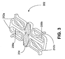
図3は、MEMSスキャナ202の別の代替実施形態を示す。図3の例示的な実施形態では、てこ部材212aおよび212bは曲がりくねった形状で形成される。てこ部材の遠位端は、上述したように典型的には取付パッドに、あるいは周辺フレーム部材に接合する。理解されるように、てこ部材の幾何学形状は実質的に変更されてもよい。
FIG. 3 shows another alternative embodiment of the
図4は、周期的な駆動信号が印加された場合の図2AのMEMSスキャナの動的応答を例証するグラフを示す。曲線402は、周期的な駆動周波数406に応じて変わる振幅応答特性404を示す。曲線408は、同じ周期的な駆動周波数の軸406に対してプロットされた、スキャナ対駆動の位相410を示す。曲線402を調べると、回転モードにあるMEMSスキャナの共振周波数に対応して、約5kHzで応答のピークが見られる。ピークのサイズは相対的な方式でプロットされているが、これは、例示的な実施形態では、受容可能な駆動電力で±20°の機械走査角を生成するのに十分に高い。4つのアクチュエータの実施形態では、振幅が0から25〜30ボルトである5kHzの正弦波に近い駆動波形により、±20°の機械走査角が得られる。
FIG. 4 shows a graph illustrating the dynamic response of the MEMS scanner of FIG. 2A when a periodic drive signal is applied. A
65〜70kHzの第2のピークは、圧電スタックアクチュエータの共振挙動に対応する。 The second peak at 65-70 kHz corresponds to the resonant behavior of the piezoelectric stack actuator.
曲線408は、駆動信号対MEMSスキャナ応答の位相関係が共振点でどのように反転するかを示す。5kHz未満では、位相関係(駆動対応答)は0°である。5kHzより上であるが第2のピーク未満では、位相関係は−180°である。主要な共振ピークでは、図示されるように、位相関係は反転し、−90°(駆動に遅れる応答)を通る。第2のピークより上では、システムの応答は低下し、また位相特性は再び反転して、ピーク未満での−180°から、第2の共振ピークで−270°(+90°)を通って、第2の共振ピークより上の周波数では−360°(0°)になる。効率を最大限にするために、主要な共振ピークで、またはその近くでMEMSスキャナを動作させるのが有利なことが分かっている。
5kHzでの動作では、MEMSスキャナの共振周波数は、5kHzより数ヘルツ上になるように、典型的には室温で5.001〜5.005kHzの範囲内に調整される。そのような調整は、参考として組み込まれる米国特許第6,245,590号(名称「周波数調整可能な共振スキャナおよび製造方法(FREQUENCY TUNABLE RESONANT SCANNER AND METHOD OF MAKING)」、本願と同一出願人による)に記載された方法によって達成されてもよい。工場へ有利と分かった、少量のエポキシ樹脂の形態の走査プレートに重りを付加する方法を用いて、共振周波数を工場で調整するのが有利であることが分かっている。共振周波数をほぼ5.000kHzにするために、共振周波数の能動的熱的調整が使用される。 For operation at 5 kHz, the resonant frequency of the MEMS scanner is typically adjusted within the range of 5.001 to 5.005 kHz at room temperature to be several hertz above 5 kHz. Such adjustment is described in US Pat. No. 6,245,590, incorporated by reference (named “FREEQUENCY TUNABLE RESONANT SCANNER AND METHOD OF MAKING”, by the same applicant as this application). May be achieved by the method described in. It has been found advantageous to adjust the resonant frequency at the factory using a method that adds weight to a scan plate in the form of a small amount of epoxy resin, which has proven advantageous to the factory. In order to bring the resonance frequency to approximately 5.000 kHz, active thermal adjustment of the resonance frequency is used.
図5Aは、100mmのシリコンウェハ502上の、MEMSスキャナ202a、202b、202c、202d、202e、および202fの基本型のレイアウトを示す。図から分かるように、MEMSスキャナには、互いに噛み合わされた取付パッドおよびミラーが稠密に詰め込まれる。そのようなレイアウトの1つの理由は、1つのウェハ当たりの歩留まりを最大限にすることである。図から分かるように、図5Aに示されるスキャナ202の走査プレートは、短く広いアスペクト比で形成される。
FIG. 5A shows a basic layout of
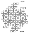
図5Bは、100mmのシリコンウェハから作製するためのMEMSスキャナの代替レイアウトを示す。スキャナの寸法、特にねじりアームの長さは、図5Aのレイアウトに比べて、より効率的に互いに噛み合わせて詰め込むように調節されている。より大きなウェハにデバイスが稠密に詰め込まれてもよい。 FIG. 5B shows an alternative layout of a MEMS scanner for making from a 100 mm silicon wafer. The dimensions of the scanner, and in particular the length of the torsion arms, are adjusted to engage and pack together more efficiently than the layout of FIG. 5A. Devices may be densely packed into larger wafers.
用語「互いに噛み合わされた」は、1以上の隣接する半導体デバイスを切断することなく、1つの半導体デバイスの周りに正方形またはダイを描くことができないことを意味する。すなわち、1以上の隣接する半導体デバイスは、ダイシングソーを用いて半導体デバイスの周りに形成することができる幾何学図形の輪郭の中に入り込む。深掘反応性イオンエッチング(DRIE)または他のプロセス工程などのエッチング工程は、ほぼ完全にウェハからスキャナを解放するのに使用される。各デバイスの周りに形成された二重線は、デバイスの周りに形成された「堀」の縁部を示す。スキャナをウェハに周期的に接続する非常に微細なシリコン「ブリッジ」が見られる。スキャナを解放するために、これらのブリッジは単に破断され、スキャナが抜き出される。ブリッジの幅は、通常は、デバイス全体にわたって割れ目が広がるのを回避するのに十分に狭くされる。 The term “engaged with each other” means that a square or die cannot be drawn around one semiconductor device without cutting one or more adjacent semiconductor devices. That is, one or more adjacent semiconductor devices enter a contour of a geometric figure that can be formed around the semiconductor device using a dicing saw. Etching steps such as deep reactive ion etching (DRIE) or other process steps are used to release the scanner from the wafer almost completely. A double line formed around each device indicates the edge of the “moat” formed around the device. There are very fine silicon “bridges” that periodically connect the scanner to the wafer. To release the scanner, these bridges are simply broken and the scanner is extracted. The width of the bridge is usually narrow enough to avoid spreading cracks throughout the device.
代替実施形態では、金属の層はめっきされ、または、絶縁体ウェハはDRIEの前にシリコンウェハの背面に接合される。DRIEは、シリコンウェハをエッチングするのに使用される。その後、金属または絶縁体の層は、ウェハの中にスキャナを保持してもよい。金属は、スキャナを除去するために裂かれてもよい。あるいは、金属または絶縁体は、部品を解放するためにエッチングで除去されてもよい。一実施形態では、アルミニウムが金属安定化層に使用される。一実施形態では、PYREX(登録商標)ガラスが絶縁体安定化層に使用される。そのような安定化層が使用される場合、成形品を適所に保持するために、シリコンブリッジが併用されてもよい。あるいは、シリコンブリッジは除外されてもよい。 In an alternative embodiment, the metal layer is plated or the insulator wafer is bonded to the backside of the silicon wafer prior to DRIE. DRIE is used to etch silicon wafers. The metal or insulator layer may then hold the scanner in the wafer. The metal may be cleaved to remove the scanner. Alternatively, the metal or insulator may be etched away to release the part. In one embodiment, aluminum is used for the metal stabilization layer. In one embodiment, PYREX® glass is used for the insulator stabilization layer. When such a stabilization layer is used, a silicon bridge may be used in combination to hold the molded article in place. Alternatively, silicon bridges may be excluded.
図5Aは、「T」字形の端部がミラーの方にずれた、代替のてこ部材212の設計をさらに示す。
FIG. 5A further illustrates an
いくつかの実施形態によるMEMSスキャナ202の作製は、上述したようなドープチャネルまたは電荷キャリア層の形成を含んでいてもよい。1〜10Ωcmのバルク抵抗率を有するリン添加シリコンウェハが使用される。リン添加シリコンウェハは、4mAの最大電流で30KeVで加速された、5×10¹⁵リン31原子/cm2のドーズ量で注入される。リンのドーズ量は、1000℃で45分間駆動される。結果として得られるドープチャネルは、約0.5μmの深さまで深くドープされて、ドーピング濃度およびそれに伴う抵抗率が深さに応じて変わる、段階的なチャネルを形成する。これらの条件では、ウェハ表面は、約1×1020リン31原子/cm3のドーピング濃度を有し、約0.001Ωcmの抵抗率をもたらし、それにより、0.5μmの深さで約1×1015原子/cm3(または1−10Ωcm)のウェハのバックグラウンドが得られる。
Fabrication of
ドープチャネルは、電荷キャリアが金属層からシリコン内に移動するための導管を作る。後述するように、ジュール加熱を作るために、MEMSスキャナ202に電流が印加されてもよい。図2Aのスキャナの例示的な実施形態では、例えば、取付パッド214a、214bは、ヒーターアンプによって正電圧に駆動されてもよい。ヒーターのリード線は、取付アセンブリおよび/または取付パッド自体上の金属化層に結合されてもよい。例示的な一実施形態によれば、電流は、取付パッド214a、214bを被覆する金属層に沿って流れ、金属の下に形成されたドープチャネルを介してシリコン内に移動する。電流は次に、てこ部材212aおよびねじりアーム206aを介してシリコン内を流れ、それにより、主にねじりアーム206aの中で局所的な加熱を形成する。(電流フローはてこ部材212aの両方のアームに沿って分割されるので、てこ部材内のジュール加熱は低減される。)ねじりアーム206aがドープチャネル220aにぶつかるところで、電流は、シリコンから流れ、ドープチャネル220aに重なって形成された金属層内に上向きに入る。電流は、中央サスペンションコネクタ218aを横切り、走査プレート204上に形成されたミラーの金属を横切り、中央サスペンションコネクタ218bを横切って流れるので、それらの構造内のジュール加熱が回避される。金属層がドープチャネル220bと重なり合うところで、電流は、金属から流れ、シリコン内に下向きに入る。電流は、ねじりアーム206bおよびてこ部材212bを通って流れ、やはりジュール加熱を(主にねじりアーム内で)生じさせる。電流は次に、取付パッド214c、214d上に形成されたドープチャネルを通って流れ、金属層に上向きに入り、そこで、地面近くで保持されたヒーターのリード線の第2の組によって電流が収集される。当該技術分野では知られているように、図示された方向のホール移動あるいは反対方向の電子移動は、そのような電流フローを形成してもよい。
The doped channel creates a conduit for charge carriers to move from the metal layer into the silicon. As described below, a current may be applied to the
場合によっては、図2A、2B、3、5A、および5Bで例証されるスキャナ設計の有利な態様は、作製の際に最小限の数のプロセス工程が用いられてもよいようなものである。範囲の厚さを低減する、または隆起したリブを生成するために、スキャナは、部分エッチングがなされていない完全な厚さのシリコンウェハから完全に形成されてもよい。ミラーに対応する金属被覆のパターンは、ウェハ502の前面に形成される。一実施形態によれば、金の金属被覆がミラーに使用される。背面金属被覆はウェハ502の背面上に形成される。一実施形態によれば、アルミニウムが背面金属被覆層に使用される。次に、半導体デバイスおよびその間のエッチングされていない範囲に対応するフォトレジストパターンが、ウェハの前面に形成され、露出範囲が深くエッチングされる。一実施形態では、DRIEが、ウェハを介して垂直壁をエッチングするのに使用される。ウェハの背面は、エッチングの間極低温に冷却され、また、アルミニウムの背面金属被覆の高い熱伝導率によって、DRIEエッチングは、シリコンウェハの背面表面に達すると停止される。いくつかの実施形態では、スキャナ形状は、エッチングされた輪郭の後部を架橋する薄いアルミニウム層によってウェハ内に保持される。他の実施形態では、シリコンの薄いブリッジが、部品を適所に保持する助けとなる。アルミニウムの背面金属被覆がエッチングで除去され、フォトレジストが除去される。スキャナはそれによって自由になり、あるいは、シリコンブリッジが使用されている場合、ウェハから取り除かれ、深くエッチングされた範囲全体にわたってブリッジを壊すことによって単独にされてもよい。ディープエッチングを用いて部品を解放することにより、ダイシングが回避されてもよい。
In some cases, the advantageous aspects of the scanner design illustrated in FIGS. 2A, 2B, 3, 5A, and 5B are such that a minimal number of process steps may be used in fabrication. In order to reduce the thickness of the area or produce raised ribs, the scanner may be fully formed from a full thickness silicon wafer that has not been partially etched. A metallization pattern corresponding to the mirror is formed on the front surface of the
図6は、MEMSスキャナのためのアクチュエータ構成を示す。共通の取付基部604上に設置された一対の市販の圧電スタック602aおよび602bは、第1の絶縁体606a、606bそれぞれを介して、MEMSスキャナ202の取付パッド214a、214bを支持する。それぞれの位置から、圧電スタック602a、602bは、交互に電気的に圧縮および拡張されて、ねじりアーム206a、206bによって画定される回転軸210の周りでの、取付パッド214a、214bの周期的な回転を生成してもよい。同様に、走査プレート204の横方向軸に実質的に平行な横方向軸の周りでMEMSスキャナ202を回転させるために、圧電スタック602a、602bの共通モード活性化が用いられてもよい。
FIG. 6 shows an actuator configuration for the MEMS scanner. A pair of commercially available
MEMSスキャナ202と圧電アクチュエータスタック602a、602bとの間の接触を維持するために、各クランプまたは加圧アセンブリ608aおよび608b(608bは図示なし)が、取付パッド214a、214bを、アクチュエータスタックに対して下向きに押し付ける。クランプ608bは、明瞭にするため図6から省略される。図示されるように、クランプ608は、(アセンブリの底部から始まり、また取り付けパッド214と接触して)第1の圧力板610、任意直列円板ばね612、第2の圧力板614、第2の絶縁体616、および第3の圧力板618を含む。一実施形態では、第1の圧力板601の縁部は、図示されるように加圧アセンブリから外に延びる。後述するように、これによって、ヒーターワイヤーまたはリード線のための任意の結合位置が提供される。直列円板ばね612は、SPRINGMASTERS #D63203などの市販のタイプのものであり、剛性は比較的低いが高い(>>5kHz)の固有共振周波数を有するように選択される。用途の要件によって、一連の2つのばね、または異なる数のばねが使用されても、あるいはばねが全くなくてもよい。第1および第2の圧力板610および614は、直列円板ばね612を押し付けるための堅牢な表面を提供する。第2の絶縁体616は、MEMSスキャナ202の電気的絶縁を提供する。第1および第2絶縁体606、616は、PYREX(登録商標)ガラスなどの、適切な密度、電気的絶縁能力、および圧縮強度を備えた材料から形成される。第1および第2の圧力板610、614は、鋼などの、好適な導電性と、圧縮強度、じん性、および密度などの物理的性質とを有する材料から形成される。第3の圧力板618は、第2の絶縁体616に取付表面を提供し、アセンブリをハウジング(図示なし)に接続する。好ましくは鋼から形成された3番目の圧力板618は、取付および調整ねじ(図示なし)を受け入れるためのボア620を含む。当業者であれば理解できるように、代替のまたは修正されたクランプが使用されてもよい。
To maintain contact between the
代替実施形態では、直列円板ばね612が加圧アセンブリ608から省略されてもよいことが分かっている。そのような修正には、組立ての容易さおよびコストに関して利点がある場合もあるが、駆動効率をある程度損なうことがある。
In alternative embodiments, it has been found that the
加圧アセンブリ608の1以上の構成要素は、ハウジングに任意に合わせられるか、そうでなければ、実質的に固定の回転関係で保持されてもよい。これにより、取付および調整ねじの調節中にアセンブリを介して伝達されるトルク負荷が低減または排除される。加圧アセンブリ608を介して大幅にトルク負荷を低減または排除することによって、組立て中にMEMSスキャナの取付パッド214に実質的にゼロのトルク負荷が印加され、それにより、取付パッド214のわずかな回転から生じる、共振周波数および/または走査角度範囲の偶発的な変化から、MEMSスキャナ202が保護される。
One or more components of the pressure assembly 608 may be optionally mated to the housing or otherwise held in a substantially fixed rotational relationship. This reduces or eliminates the torque load transmitted through the assembly during adjustment of the mounting and adjustment screw. By substantially reducing or eliminating the torque load through the pressure assembly 608, a substantially zero torque load is applied to the MEMS scanner mounting pad 214 during assembly, thereby causing a slight rotation of the mounting pad 214. The
図7はピエゾスタックアクチュエータ602の図である。そのようなアクチュエータは、http://www.physikinstrumente.deのモデルPICMA 885.10などの、複数の供給源から入手可能である。
FIG. 7 is a diagram of a
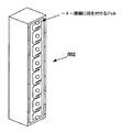
図8および9は、LBP、バーコードスキャナ、LIDAR、走査レーザーレベルなどで使用される、MEMSスキャナハウジング802の図である。2つの前板804a、804bは、取付ねじ808a、808b、808c、808dで後部ハウジング806に固定される。MEMSスキャナ202は、適切な量の回転を可能にするその中の空洞内に保持される。ねじ切りされた調整ねじ穴810a、810b、810c、および810dは、対応する調整ねじ受け入れボア620(図6に示される)内に突出する調整ねじ(図示なし)を受け入れる。組立て中に、調整ねじは回転されて、直列円板ばね612(図示なし)上に適切な量の予荷重を提供する。動作中のMEMSスキャナの挙動は、後部ハウジング806の頂部に形成されたMEMS観察ポート812を介して観察することができる。MEMSスキャナアセンブリ802は、ハウジング806内に形成された取付タブ814a、814bを介して、LBPの露光ユニットに固定される。
FIGS. 8 and 9 are diagrams of a
クランプ608を使用してハウジング802内でMEMSスキャナ202を固定することによって、「浮遊」するマウントが得られ、取付パッド214が互いに対して少し移動することが可能になる。いくつかの実施形態では、組立て中のクランプ608のわずかな捻回により、取付パッド214のわずかな面内捻回を得ることができる。これにより、MEMSスキャナのてこ部材および/またはねじりアームにおける望ましくない残留応力が生じる場合がある。そのような捻回は、取り付けられたスキャナを、低減された走査角で数時間作動または「通電」することによって、低減または排除される場合がある。例示的な一実施形態では、スキャナは、半分の振幅で約4時間作動される。通電プロセスは、てこ部材および/またはねじりアームの機械的欠陥に関連した「初期」欠陥の発生を低減することができる。あるいは、スキャナアセンブリを通電する必要性を低減または排除するために、ねじれが低減されたクランプアセンブリ設計に置き換えられてもよい。
Using the clamp 608 to secure the
MEMSスキャナ202は、1つ1つが各取付パッド214a、214b、214c、および214dの下にある、4つの圧電スタック602によって駆動されてもよい。あるいは、MEMSスキャナの一端は固定位置で保持され、つまり、取付パッド214cおよび214dが安定した取付ポイントに対して固定されてもよく、また、MEMSスキャナの他端は圧電アクチュエータで駆動され、つまり、取付パッド214aおよび214bがそれぞれ、図6に示されるように圧電スタックに対して固定されてもよい。第3の代替例では、取付パッドの3つが固定の安定した取付ポイントに固定され、1つの圧電アクチュエータが使用される。典型的には、その選択は、コスト対アクチュエータの電力要件に依存する。理解されるように、同様の考察は、図2Bまたは3に示されるようなMEMSスキャナ設計202に当てはまる。
The
上述したように、MEMSスキャナは、所望の動作周波数の数ヘルツ以内の共振周波数を有するように調整される。図4の曲線402から理解されるように、共振周波数を少し変化させることにより、(所与の周期的な動作電圧に対して)回転振幅の比較的大幅な変化を得ることができる。本発明者らは、MEMSデバイスの制御された加熱によって、MEMSスキャナが外側フレームを有さない例示的な実施形態であっても、共振周波数、したがって動作振幅がさらに調整されることを見出した。図6を再び参照すると、クランプ608b(図示なし)の対応する圧力板が行うように、クランプ608aの第1の圧力板610上の拡張タブは、ヒーター線を受入れる。同様に、取付パッド214cおよび214d(やはり図示なし)に隣接する対応する圧力板もまた、ヒーター線を受け入れる。ヒーター線は、第1の圧力板610の金めっきされた拡張タブにはんだ付けすることによって、例えば取付パッド214上に形成された金属化シリコン結合パッドにはんだ付けすることによって、あるいは当業者に明白であるような他の方法によって取り付けられてもよい。
As described above, the MEMS scanner is tuned to have a resonant frequency within a few hertz of the desired operating frequency. As can be seen from
MEMSスキャナの一端にある取付パッドまたはクランプの両方に、ヒーターのリード線が取り付けられる場合、電流がその間を流れるのを回避するために、そのような隣接するリード線を同じ電位に保つことが好ましい。対照的に、MEMSスキャナの他端にあるヒーターのリード線(単数または複数)が異なる電圧まで駆動されて、ねじりアームに沿って、かつそれを介して電流フローを作成してもよい。 If heater leads are attached to both mounting pads or clamps at one end of the MEMS scanner, it is preferable to keep such adjacent leads at the same potential to avoid current flowing between them. . In contrast, the heater lead (s) at the other end of the MEMS scanner may be driven to a different voltage to create a current flow along and through the torsion arm.
使用中、走査振幅はセンサによって監視され、また、スキャナ202の2つの端部(取付パッド214aおよび214bがその一端を形成し、取付パッド214cおよび214dが他端を形成する)間の電位が調節される。シリコン材料自体および上述したドープチャネルの電流フローに対する抵抗、および特にねじりアーム206a、206bによって、加熱が引き起こされる。高温であるほど、ねじりアームの「軟化」およびそれに対応する共振周波数の低下が引き起こされる。したがって、共振周波数が周期的な駆動信号周波数よりも上の場合、加熱が増加されて、MEMSスキャナの温度が上昇し、それによって、駆動信号周波数と合致するように共振周波数が調整されてもよい。同様に、MEMSスキャナの共振周波数が駆動信号周波数よりも下になる場合、加熱が低減され、それによってデバイスが冷却され、駆動信号周波数と合致するようにその共振周波数が上昇されてもよい。代替実施形態では、熱の調整は、所与のシステム設計については、スキャナがその共振周波数で正確に動作されない場合でも、走査振幅を変更するために使用されてもよい。
In use, the scan amplitude is monitored by the sensor and the potential between the two ends of the scanner 202 (the mounting
0〜1.5Wのチューニング電力が約8Hzの共振周波数同調範囲を提供できることが、実験によって測定されている。この範囲は、恐らく動作中に冷却をもたらすスキャナ上の気流が原因で、より高い走査周波数では多少低く、より低い走査周波数では多少高い場合がある。 It has been experimentally determined that 0-1.5 W tuning power can provide a resonant frequency tuning range of about 8 Hz. This range may be somewhat lower at higher scan frequencies and somewhat higher at lower scan frequencies, possibly due to airflow over the scanner that provides cooling during operation.
次に図10を参照すると、MEMSスキャナを駆動する制御システム1002を示すブロック図が示される。多くの用途では、MEMSスキャナの走査の位相および振幅を正確に制御することは有利である。バーコードスキャナ、レーザーカメラ、走査ビームディスプレイ、電子写真式プリンタなどの走査ビームの用途は、MEMSスキャナの位相および/または振幅を正確に制御することで利益を得ることができる。
Referring now to FIG. 10, a block diagram illustrating a
同様に、スキャナ共振周波数を正確に制御することで、従来典型的な慣例であった多少ずれた共振ではなく、その共振周波数でスキャナを動作可能にすることによって、消費電力を最小限にし、恐らくは実現可能な特定の応用も行うことができる。 Similarly, precise control of the scanner resonance frequency minimizes power consumption, possibly by enabling the scanner to operate at that resonance frequency rather than the somewhat off-track resonance that was typical of the traditional practice. Specific realizable applications can also be made.
図10の制御システム1002のブロック図は、MEMSスキャナを駆動し制御するための、それぞれ中程度の、短い、および長い破線で輪郭が描かれた、振幅制御サーボループ1004、位相制御サーボループ1006、および共振周波数制御サーボループ1008という、3つの重なり合うサーボループを含む。
The block diagram of the
最初に振幅制御ループ1004を参照すると、低電圧駆動信号1009は高圧増幅器1010によって増幅され、圧電ドライバスタック602の形態の1以上のアクチュエータを駆動する周期的な高電圧駆動信号1011を生成して、共振MEMS走査ミラー202の周期的な振動を引き起こす。理解されるように、圧電アクチュエータ602の代わりに、磁気タイプ、静電気タイプ、熱タイプ、および他のタイプのアクチュエータなどの、代替アクチュエータ技術を用いることができる。
Referring initially to the
MEMS走査ミラー202の位相、振幅、位置、および/または速度を監視するために、様々な技術を使用することができる。例示的な実施形態では、ミラーによって偏向されたビームは約20%のオーバースキャンを含み、したがって画像化領域の縁部は80%の走査で終了する。一対の隣接するセンサ領域を含む光学検波器1012は、その中央点(センサ範囲間の領域の中心)を走査範囲の85%の位置に有して配置される。1つのセンサ領域からの出力は、コンバータ1014によって別のセンサ領域の出力から減算される。コンバータ1014は、走査振幅信号1016としてのビームがスキャン範囲の中央の85%を越える時間量に比例した陰電圧を出力する、差動およびパルス幅−電圧コンバータである。
Various techniques can be used to monitor the phase, amplitude, position, and / or velocity of the
マイクロプロセッサ1018は、加算器1022中の走査振幅信号1016に加算される振幅設定値電圧信号1020を設定して、生の振幅誤差信号1024を生成する。したがって、走査振幅が所望よりも大きい場合、負の走査振幅信号1016の絶対量は設定値信号1020の絶対量よりも大きくなり、生の振幅誤差信号1024は負の数値になる。反対に、走査振幅が所望よりも小さい場合、負の走査振幅信号1016の絶対量は設定値信号1020の絶対量よりも小さくなり、生の振幅誤差信号1024は正の数値になる。
The
生の振幅誤差信号1024は、比例積分コントローラ(PIC)1026に供給される。PIC1026は、条件付き振幅誤差信号1028を生成する。PIC1026は、走査振幅の変動に対するシステム応答を減衰するように作用する。これは、生の振幅誤差信号1024電圧におけるばらつきを平均化し、また、振幅誤差の変化がフィードバックされて高電圧駆動信号に影響する速度を制御するように作用し、それによって、振幅制御サーボループ1004の安定性および性能を改善する。
The raw
生の駆動信号1030は、MEMSスキャナを駆動するための、名目上の位相が補正された信号である周期的な低電圧信号である。生のドライブ信号1030は、利得回路1032で受け取られ、乗算されて、低電圧駆動信号1009を生成する。したがって、測定されたMEMSスキャナ202の振幅が低すぎる場合、条件付き振幅誤差信号1028は比較的高い電圧であり、利得回路1032中で生の駆動信号1030で乗算されると比較的低い振幅の低電圧駆動信号1009を生成する。測定されたMEMSスキャナの振幅が高すぎる場合、条件付き振幅誤差信号1028は比較的低い電圧であり、利得回路1032中で生の駆動信号1030で乗算されると比較的低い振幅の低電圧駆動信号1009を生成する。いずれかの場合、それによって、走査振幅を設定値電圧信号1020としてマイクロプロセッサ1018によって所望の設定値に戻す役割を果たす。
The
位相制御サーボループ1006は位相ロックループとして動作する。振幅制御サーボループ1004に関連して上述したコンバータ1014は、水平同期信号1035としてホストコントローラにも戻される位相マーク信号1034を生成する。位相マーク信号1034は、1つの縁部、すなわち1つの走査方向を用いて減算された検出器ペア信号から生成される。基準信号1036と位相マーク信号1034の同様の縁部は、第1の位相周波数検出器1038によって比較される。第1の位相周波数検出器1038は、生の位相誤差信号1040上の周期的なスパイクを生成し、そのスパイクの幅は位相誤差に比例し、またそのスパイクの符号は、位相マーク信号1034が基準信号1036に対して早いか遅いかを示す。
The phase
第1の低域フィルタ1042は、第1の条件付き位相誤差信号1044として生の位相誤差信号1040上の周期的なスパイクを直流電圧に変換する。第1の低域フィルタ1042は、位相マーク1034が基準信号1036に対して早い場合、第1の条件付き位相誤差信号1044を比較的低い値に設定する。反対に、位相マーク1034が基準信号1036に対して遅い場合、第1の低域フィルタ1042は第1の位相誤差信号1044を比較的高い値に設定する。
The first
第1の条件付き位相誤差信号1044は、電圧制御駆動波形生成器1046に渡される。第1の条件付き位相誤差信号1044の電圧により、電圧制御駆動波形生成器1046によって出力される生の駆動信号1030の周波数が決まる。
The first conditional
したがって、位相マーク信号1034が基準信号1036に対して早い場合、第1の位相周波数検出器1038は生の位相誤差信号1040上に負のスパイクを出力し、そのスパイクの幅は、位相マーク信号1034と基準信号1036の間の誤差の大きさに比例する。生の位相誤差信号1040上の一連の負のスパイクは、第1の低域フィルタ1042を駆動して、第1の条件付き位相誤差信号1044上に比較的低い電圧を出力し、その電圧は、生の位相誤差信号1040上のスパイク幅が狭い場合には適度に低く、スパイク幅が広い場合は電圧はさらに極端(低い)である。第1の条件付き位相誤差信号1044上の低電圧により、電圧制御駆動波形生成器1046から、より低い周波数の生の駆動信号1030が出力され、位相の小さな偏差(第1の条件付き位相誤差信号1044上の適度に低い電圧)は周波数の適度な減少を引き起こし、位相の比較的大きな偏差(第1の条件付き位相誤差信号1044上の低電圧)は周波数のより大きな減少を引き起こす。より低い周波数は、MEMSミラーの位相を遅らせて、位相マーク信号1034がいくらか後で出力されるようにし、それにより、位相マーク信号1034が基準信号1036と同調するように戻し、基準信号1036に位相ロックをもたらす役割を果たす。
Thus, if the phase mark signal 1034 is earlier than the
位相マーク信号1034が基準信号1036に対して遅い場合、第1の条件付き位相誤差信号1044の電圧が増加され、その結果生の駆動信号1030の駆動周波数が増加し、同様に位相マーク信号1034が基準信号1036と同調するように戻す。低域フィルタ1042の時定数は、位相サーボ制御システム1006に減衰をもたらす役割を果たす。
If the phase mark signal 1034 is slower than the
次に共振周波数サーボ制御ループ1008を参照すると、駆動信号とスキャナ応答の相対的位相は、MEMSスキャナの共振周波数を調節するのに使用される。図4に関連して上述したように、MEMSスキャナの応答位相は、曲線408で示されるような周波数を備えた駆動位相によって変わる。スキャナ振幅応答特性曲線402における主要なスパイクでは、駆動信号とスキャナ応答の間の位相関係は、主要な共振ピークでの−90°を通過して、主要な共振ピークの下の同相(0°)から主要な共振ピークの上の−180°異相に急速に反転する。共振周波数サーボ制御ループ1008は、この位相応答の変化を利用して、MEMSスキャナの共振応答を駆動周波数と合致するように調整しておく。
Referring now to the resonant frequency
共振応答における主要なピークでは、駆動信号に対するMEMSデバイスの位相特性は、その共振ピークで−90°を通過して0°から−180°に急速にシフトする。この反転は、図4では実質的に瞬間的なものとして示される(図の広い周波数範囲に起因する)が、実際には反転は数ヘルツにわたって起こる。したがって、MEMSスキャナがその共振ピークで動作していることを示す、−90°での位相マーク信号1034と駆動信号1030の間の位相のずれを維持することが望ましい。
At the main peak in the resonant response, the phase characteristic of the MEMS device relative to the drive signal shifts rapidly from 0 ° to −180 ° through −90 ° at the resonant peak. This inversion is shown in FIG. 4 as being substantially instantaneous (due to the wide frequency range of the figure), but in fact the inversion occurs over several hertz. Therefore, it is desirable to maintain a phase shift between the phase mark signal 1034 and the
例示的な一実施形態によれば、MEMSスキャナ共振周波数の温度依存性は利点をもたらすために使用される。位相マーク信号1034は、第2の低域フィルタ1050と協働して第2の条件付き位相誤差信号1052を生成する、第2の位相周波数検出器1048によって生の駆動信号1030と比較される。第2の位相周波数検出器1048は、位相マーク信号1034と駆動信号1030の間の位相のずれが−90°の場合に、第2の条件付き位相誤差信号上に公称電圧を出力するように設定され、相対的位相が−90°〜−180°のときに電圧を上昇させ、相対的位相が0°〜−90°のときに電圧を減少させる。公称電圧は、MEMSスキャナ202を通る電流を設定して、共振周波数が駆動周波数と合致するようにするのに適切な電圧である。例示的な一実施形態によれば、かつ上述したように、MEMSスキャナは、室温で主要な共振ピークが名目上の動作周波数の数ヘルツ上になるように、製造中に調整される。その後、電流が共振周波数サーボ制御ループ1008によって供給されて、図示されるような駆動周波数1030と合致するように、MEMSスキャナ202の共振周波数が低減される。
According to one exemplary embodiment, the temperature dependence of the MEMS scanner resonance frequency is used to provide an advantage. The phase mark signal 1034 is compared to the
スイッチ1054は、システムが動作中(起動後)のときには通常閉じている。したがって、第2の条件付き位相誤差信号1052上の電圧はヒーターアンプ1056に渡される。位相マーク信号1034と駆動信号1030の間の相対的位相が−90°〜−180°の場合、第2の位相周波数検出器1048と第2の低域フィルタ1050が協働して、第2の条件付き位相誤差信号1052上の電圧を−90°からの偏差の程度に比例して上昇させる。次に、ミラー応答の位相が駆動位相よりも遅れている場合に、ヒーターアンプ1056が駆動されてMEMSミラー202の両端間の電圧を設定する。そのような条件は、駆動周波数よりも高いミラーの共振ピークに対応する。
上述したように、半導体のMEMSスキャナ202の両端間の電位を増加させることにより、スキャナ内のジュール加熱が増加し、それによってその温度が上昇する。MEMSスキャナ202の温度が上昇することで、そのピーク共振周波数が低下する。したがって、MEMSスキャナ202のピーク共振周波数が駆動信号周波数よりも上の場合、その位相は、90°よりもいくらか低い分だけ駆動信号の位相に遅れる傾向があり、共振周波数サーボ制御ループ1008は、スキャナ温度の上昇をもたらし、位相差を適切な関係にし、それにより、MEMSスキャナ202のピーク共振周波数は駆動信号周波数と合致するように低減される。反対に、MEMSスキャナ202がそのピーク共振周波数を駆動周波数よりも下に低下させるのに十分に加熱されると、その位相は90°よりもいくらか多い分だけ駆動信号に遅れる傾向があり、制御ループはヒーターの電流フローを低減し、それにより、ピーク共振周波数が、駆動周波数と合致するように、位相関係が再び−90°になるまで少し上昇される。この制御ループにより、スキャナが実質的にそのピーク共振周波数で動作できるようになり、したがってアクチュエータの所要電力が最小限になる。
As described above, increasing the potential across the
再び図10を参照すると、マイクロプロセッサ1018は、通信手段1058を含み、また周囲温度センサ1060を含む。第2の条件付き位相誤差信号1052および位相マーク信号1034がマイクロプロセッサ1018に送られ、制御線1062および1064が、スイッチ1054およびヒーターアンプ1056にそれぞれ接続していることも分かる。これらの特徴の多くまたはすべてはシステムの起動中に使用される。
Referring again to FIG. 10, the
図11は、図10で示されるシステム1002によって使用される起動方法を示すフローチャートである。プロセス1102に対応するアイドル状態中に電源が入れられると、位相制御ループ1006および共振周波数制御ループ1008は両方とも模擬フィードバックを使用して作動される。マイクロプロセッサ1018は、最初にライン1044上で電圧を設定し、それが電圧制御波形発生器1046に送られる。生の駆動信号ライン1032は次に、第1の位相周波数検出器1038に模擬位相マーク信号1034を出力するコンバータ(図示なし)に対する入力として働く。第1の位相周波数検出器1038は次に、模擬位相マーク信号1034を基準信号1036と比較し、生の位相誤差信号1040を第1の低域フィルタ1042に出力し、それは次に、条件付き位相誤差信号1044上の電圧を設定する。したがって、位相サーボ制御ループ1006は、MEMSスキャナの移動および検出とは無関係に作動し続ける。
FIG. 11 is a flowchart illustrating a startup method used by the
共振周波数サーボ制御ループ1008を作動させるために、マイクロプロセッサ1018は、周囲温度センサ1060から周囲温度を読み取る。温度センサ値は、共振周波数ルックアップテーブル(LUT)(図示なし)に対するインデックスの役割を果たすデジタル値に変換される。結果として得られる共振周波数のLUT値は、合成された共振周波数電圧信号1064を出力してヒーターアンプ1056を駆動する、D/A変換器(DAC)を駆動する。動作中のように、ヒーターアンプ1056は次にMEMSスキャナ202の両端間の電圧を設定し、また、ジュール加熱によって、MEMSスキャナの温度が共振周波数LUT値に対応する温度まで上昇される。いくつかの実施形態では、共振周波数LUTは、目標動作周波数、例えば5kHzにその共振周波数を調整するのに必要なスキャナ温度を決定することにより、工場較正工程として、各MEMSスキャナ202に対して導き出される。他の実施形態では、LUTは、MEMSスキャナのバッチまたはすべてのMEMSスキャナに対して設定することができる。したがって、プロセス1102に対応するアイドル状態中に、共振周波数サーボ制御ループ1008は、MEMSスキャナ202を、その共振周波数が基準信号1036の周波数に合致するように設定された、名目上の動作温度で維持するように動作可能である。
To operate the resonant frequency
周囲温度を感知する代わりとして、温度センサ1060は、MEMSスキャナ202に熱的に結合されて、その温度を測定してもよい。
As an alternative to sensing ambient temperature, the
パワーオンアイドルプロセス1102にある間、マイクロプロセッサ1018は、条件付き工程1104で示されるように、始動信号がインターフェース1058を越えてホストコントローラから受け取られたかを判断するために確認する。「NO」の決定で示されるように、パワーオンアイドルプロセス1102は、始動信号がホストコントローラから受け取られるまで継続する。始動信号が受け取られると、埋込み型ソフトウェアは起動振幅制御プロセス1106に移る。起動振幅制御プロセス1106に入ると、マイクロプロセッサ1018は、低電圧駆動信号1009を設定して高圧増幅器1010を駆動し、最大振幅で高電圧駆動信号1011を生成し、それによって圧電スタックアクチュエータ602を過剰運転する。圧電スタックアクチュエータ602を過剰運転することで、走査振幅が非常に急速に上昇する。起動の一実施形態によれば、高電圧駆動信号1011は、0(ゼロ)〜60ボルトの振幅を備えた5kHzの基準周波数で正弦波を含む。この実施形態では、MEMSスキャナは、わずか20ミリ秒でその名目上の走査角の約90%に達するように駆動され、約0〜20ボルトのより低い名目上の定常状態駆動電圧を印加することで得られるよりも高速のシステム起動が得られる。
While in the power-on
他の実施形態では、高電圧駆動信号は、アクチュエータ602の絶縁破壊電圧の近傍までの、さらに大きな振幅で設定されてもよい。それらは、アクチュエータの熱限界を越えるのには短すぎる比較的短い時間にのみ適用されるので、高い始動駆動電圧が可能である。
In other embodiments, the high voltage drive signal may be set with a larger amplitude up to near the breakdown voltage of the
起動振幅制御プロセス1106の間、決定プロセス1108によって示されるように、システムは安定した位相マーク信号1034を探す。安定した位相マーク信号は、いくつかの連続する位相マークを平均して、それらが振幅制御サーボループ1004の要件を満たすかを判断する回路(図示なし)を監視することによって決定される。安定した位相マーク信号が存在すれば、MEMSスキャナ202が比較的一定の周波数および十分な振幅で動作し、走査ビームが光学振幅センサ1012と交差することを意味し、プロセスは、スキャナの振幅が振幅制御サーボループ1004によって制御される閉ループ振幅制御プロセス1110に移る。閉ループ振幅制御プロセス1110に入ると、上述したように、PIC1026は安定動作と合致する速度で駆動振幅に対する変更を導入する。
During the startup
閉ループ振幅制御プロセス1110が継続する一方、システムは待機して、「待機」プロセス1112で示されるようにシステムの安定化を確保する。一実施形態によれば、システムは、閉ループ位相制御プロセス1114に移る前に100ミリ秒待機し、その際、位相マーク信号1034(コンバータ1014によって生成される)は第1の位相周波数検出器1038に結合され、生の駆動信号1030から生成された合成された位相マーク信号は脱結合される。プロセス1114は、MEMSスキャナ202の周波数を基準信号1036の周波数にロックし、それにより、上述したように位相制御サーボループ1006を位相ロックループとする。
While the closed loop
閉ループ位相制御プロセス1114が進んでいる間、システムはある時間、例えば、プロセス1116で示されるように30ミリ秒休止する。待機プロセス1116が完了すると、システムは、共振周波数サーボループ1008が係合される、閉ループ共振周波数制御プロセス1118に入る。共振周波数サーボループ1008は、スイッチ1062を閉じ、マイクロプロセッサ1018からのDAC信号1064の出力を実質的に同時に止めることによって係合される。これにより、第2の条件付き位相誤差信号1052が、図10に関連して上述した方法に従ってヒーターアンプ1056を駆動する。
While the closed loop phase control process 1114 proceeds, the system pauses for some time, eg, 30 milliseconds as indicated by process 1116. When the wait process 1116 is complete, the system enters a closed loop resonant
例示的な一実施形態によれば、図11の起動プロセスによって、一般に、ホストコントローラから起動コマンドを受け取った後2秒未満以内に、走査システムの安定な動作が得られる。 According to one exemplary embodiment, the activation process of FIG. 11 generally provides stable operation of the scanning system within less than 2 seconds after receiving an activation command from the host controller.
本発明の上述の発明の開示、図面の簡単な説明、および発明を実施するための最良の形態は、読者がより容易に理解できるような形で本発明による例示的な実施形態を説明する。他の構造、方法、および等価物が本発明の範囲に含まれ得る。そのため、本明細書に記載した本発明の範囲は請求項によってのみ制限されるものとする。 The foregoing invention disclosure, brief description of the drawings, and best mode for practicing the invention describe exemplary embodiments according to the invention in a manner that is more readily understood by the reader. Other structures, methods, and equivalents may be included within the scope of the present invention. Therefore, the scope of the invention described herein is limited only by the claims.
204 走査プレート
206a、206b ねじりアーム
208a、208b サスペンションビーム
210 回転軸
212a、212b てこ部材
214a、214b 取付パッド
216a、216b、216c、216d サスペンション外部コネクタ
218a、218b サスペンション中心コネクタ
220a、220b ドープチャネル
502 ウェハ
608 クランプ
Claims (30)
前記複数の互いに噛み合わされた形状を前記半導体ウェハから除去して、不規則な輪郭を有する複数の半導体装置を生成する工程とを含む、半導体装置の製造方法。 Deep etching a plurality of meshed contours in a semiconductor wafer; and
Removing the plurality of meshed shapes from the semiconductor wafer to generate a plurality of semiconductor devices having irregular contours.
複数の互いに噛み合わされた形状がその上に形成された前記フォトマスクを使用して、前記フォトレジストを選択的に露出させる工程と、
前記半導体ウェハからフォトマスク材料を選択的に除去する工程とをさらに含む、請求項2に記載の半導体装置の製造方法。 Applying a photoresist to the semiconductor wafer;
Selectively exposing the photoresist using the photomask having a plurality of interdigitated shapes formed thereon;
The method for manufacturing a semiconductor device according to claim 2, further comprising a step of selectively removing a photomask material from the semiconductor wafer.
前記複数の互いに噛み合わされた形状を除去する工程が、前記絶縁体層の少なくとも一部分を除去することを含む、請求項1に記載の半導体装置の製造方法。 Further comprising bonding an insulator layer to the semiconductor wafer prior to deep etching;
The method for manufacturing a semiconductor device according to claim 1, wherein the step of removing the plurality of meshed shapes includes removing at least a part of the insulator layer.
前記半導体ウェハにフォトレジストを適用する工程と、
複数の互いに噛み合わされた形状がその上に形成された前記フォトマスクを使用して、前記フォトレジストを選択的に露出させる工程と、
前記半導体ウェハからフォトマスク材料を選択的に除去する工程と、
ディープエッチングプロセスを用いて前記ディープエッチングされた輪郭を生成する工程とによって生成される、請求項18に記載のシリコンウェハ。 The deep etched contours of the plurality of interdigitated shapes are
Applying a photoresist to the semiconductor wafer;
Selectively exposing the photoresist using the photomask having a plurality of interdigitated shapes formed thereon;
Selectively removing photomask material from the semiconductor wafer;
19. The silicon wafer of claim 18, wherein the silicon wafer is generated by generating the deep etched profile using a deep etching process.
Applications Claiming Priority (3)
| Application Number | Priority Date | Filing Date | Title |
|---|---|---|---|
| US54289604P | 2004-02-09 | 2004-02-09 | |
| US57113304P | 2004-05-14 | 2004-05-14 | |
| PCT/US2005/004068 WO2005078772A2 (en) | 2004-02-09 | 2005-02-09 | Method and apparatus for making a mems scanner |
Publications (2)
| Publication Number | Publication Date |
|---|---|
| JP2007525025A true JP2007525025A (en) | 2007-08-30 |
| JP2007525025A5 JP2007525025A5 (en) | 2008-03-21 |
Family
ID=34864506
Family Applications (4)
| Application Number | Title | Priority Date | Filing Date |
|---|---|---|---|
| JP2006553201A Withdrawn JP2007522528A (en) | 2004-02-09 | 2005-02-09 | High performance MEM scanner |
| JP2006552357A Withdrawn JP2007527551A (en) | 2004-02-09 | 2005-02-09 | Method and apparatus for scanning light beams |
| JP2006553203A Pending JP2007522529A (en) | 2004-02-09 | 2005-02-09 | MEMS scanning system with improved performance |
| JP2006552358A Withdrawn JP2007525025A (en) | 2004-02-09 | 2005-02-09 | Method and apparatus for manufacturing MEMS scanner |
Family Applications Before (3)
| Application Number | Title | Priority Date | Filing Date |
|---|---|---|---|
| JP2006553201A Withdrawn JP2007522528A (en) | 2004-02-09 | 2005-02-09 | High performance MEM scanner |
| JP2006552357A Withdrawn JP2007527551A (en) | 2004-02-09 | 2005-02-09 | Method and apparatus for scanning light beams |
| JP2006553203A Pending JP2007522529A (en) | 2004-02-09 | 2005-02-09 | MEMS scanning system with improved performance |
Country Status (6)
| Country | Link |
|---|---|
| US (3) | US7482730B2 (en) |
| EP (4) | EP1719012B9 (en) |
| JP (4) | JP2007522528A (en) |
| KR (4) | KR101088501B1 (en) |
| AT (1) | ATE551293T1 (en) |
| WO (4) | WO2005078506A2 (en) |
Cited By (6)
| Publication number | Priority date | Publication date | Assignee | Title |
|---|---|---|---|---|
| JP2010002637A (en) * | 2008-06-19 | 2010-01-07 | Canon Electronics Inc | Optical scanning apparatus |
| US8472096B2 (en) | 2007-11-14 | 2013-06-25 | Canon Kabushiki Kaisha | Method of manufacturing oscillator device, and optical deflector and optical instrument with oscillator device |
| JP2018520892A (en) * | 2015-05-18 | 2018-08-02 | ローベルト ボツシユ ゲゼルシヤフト ミツト ベシユレンクテル ハフツングRobert Bosch Gmbh | Micromachine type spring device and method of manufacturing micromachine type spring device |
| KR20190106216A (en) * | 2018-03-08 | 2019-09-18 | 주식회사 에스오에스랩 | Lidar scanning device capable of front and rear measurement |
| US10613224B2 (en) | 2018-01-08 | 2020-04-07 | SOS Lab co., Ltd | LiDAR device |
| US11953626B2 (en) | 2018-01-08 | 2024-04-09 | SOS Lab co., Ltd | LiDAR device |
Families Citing this family (133)
| Publication number | Priority date | Publication date | Assignee | Title |
|---|---|---|---|---|
| IL165212A (en) | 2004-11-15 | 2012-05-31 | Elbit Systems Electro Optics Elop Ltd | Device for scanning light |
| US7271821B2 (en) * | 2004-12-16 | 2007-09-18 | Marvell International Technology Ltd. | Laser printer with reduced banding artifacts |
| US7636101B2 (en) * | 2005-02-09 | 2009-12-22 | Microvision, Inc. | MEMS scanner adapted to a laser printer |
| KR100629488B1 (en) * | 2005-02-28 | 2006-09-28 | 삼성전자주식회사 | Resonator |
| KR100707194B1 (en) * | 2005-05-31 | 2007-04-13 | 삼성전자주식회사 | Laser scanner having reduced dynamic deformation |
| US7301689B2 (en) * | 2005-10-31 | 2007-11-27 | Advanced Numicro Systems, Inc. | MEMS mirror with parallel springs and arched support for beams |
| US7361900B2 (en) * | 2005-12-14 | 2008-04-22 | Northrop Grumman Corporation | “I” beam bridge interconnection for ultra-sensitive silicon sensor |
| CN101331419A (en) * | 2005-12-15 | 2008-12-24 | 皇家飞利浦电子股份有限公司 | MEMS beam scanner system and method |
| US7495833B2 (en) | 2006-02-23 | 2009-02-24 | Microvision, Inc. | Scanned beam source and systems using a scanned beam source for producing a wavelength-compensated composite beam of light |
| JP2007322466A (en) | 2006-05-30 | 2007-12-13 | Canon Inc | Optical deflector and optical equipment using the same |
| JP4316590B2 (en) | 2006-06-23 | 2009-08-19 | 株式会社東芝 | Piezoelectric drive MEMS actuator |
| JP2009545781A (en) * | 2006-08-03 | 2009-12-24 | インフェイズ テクノロジーズ インコーポレイテッド | Small single-actuator scanner for angle multiplexing with circularization and pitch correction functions |
| US8363296B2 (en) * | 2006-10-04 | 2013-01-29 | Ricoh Company, Ltd. | Optical scanning device, image forming apparatus, mirror, housing, mirror attaching method, mirror arrangement adjusting device, and mirror arrangement adjusting method |
| DE102006051207B4 (en) | 2006-10-30 | 2019-09-12 | Robert Bosch Gmbh | Micromechanical component with a micro-vibrating device and method for adjusting a component |
| US7411989B2 (en) * | 2006-12-13 | 2008-08-12 | Coherent, Inc. | Mechanically Q-switched CO2 laser |
| JP5092406B2 (en) * | 2007-01-10 | 2012-12-05 | セイコーエプソン株式会社 | Actuator, optical scanner and image forming apparatus |
| US20080197964A1 (en) * | 2007-02-21 | 2008-08-21 | Simpler Networks Inc. | Mems actuators and switches |
| US8553306B2 (en) * | 2007-03-15 | 2013-10-08 | Ricoh Company, Ltd. | Optical deflector and optical device |
| DE102008013098B4 (en) | 2007-04-02 | 2012-02-09 | Fraunhofer-Gesellschaft zur Förderung der angewandten Forschung e.V. | Micromechanical system with temperature stabilization |
| JP5608556B2 (en) * | 2007-08-10 | 2014-10-15 | ボード・オブ・リージエンツ,ザ・ユニバーシテイ・オブ・テキサス・システム | Forward imaging optical coherence tomography (OCT) system and probe |
| JP2009058616A (en) * | 2007-08-30 | 2009-03-19 | Canon Inc | Oscillating body apparatus, light deflector and image forming apparatus using the same |
| JP5007648B2 (en) * | 2007-10-12 | 2012-08-22 | セイコーエプソン株式会社 | Actuator, optical scanner and image forming apparatus |
| TWI345381B (en) * | 2007-12-31 | 2011-07-11 | E Pin Optical Industry Co Ltd | Mems scan controller with clock frequency and method of control thereof |
| JP5554895B2 (en) | 2008-02-20 | 2014-07-23 | キヤノン株式会社 | Oscillator structure and oscillator device using the oscillator structure |
| WO2009148677A2 (en) | 2008-03-11 | 2009-12-10 | The Regents Of The University Of California | Microelectromechanical system (mems) resonant switches and applications for power converters and amplifiers |
| DE102008001056A1 (en) | 2008-04-08 | 2009-10-15 | Robert Bosch Gmbh | Deflection device for a beam of an electromagnetic wave |
| TW200947164A (en) * | 2008-05-09 | 2009-11-16 | E Pin Optical Industry Co Ltd | MEMS scan controller with inherence frequency and method of control thereof |
| DE102008001896B4 (en) | 2008-05-21 | 2023-02-02 | Robert Bosch Gmbh | Micromechanical component and manufacturing method for a micromechanical component |
| DE102008001893A1 (en) | 2008-05-21 | 2009-11-26 | Robert Bosch Gmbh | Deflection device for electromagnetic radiation |
| JP5296427B2 (en) * | 2008-06-20 | 2013-09-25 | キヤノン電子株式会社 | Optical scanning device, control method therefor, image reading device, and display device |
| JP5491004B2 (en) * | 2008-06-20 | 2014-05-14 | キヤノン電子株式会社 | OPTICAL SCANNING DEVICE, IMAGE FORMING DEVICE USING THE OPTICAL SCANNING DEVICE, IMAGE READING DEVICE, AND DISPLAY DEVICE |
| KR100987779B1 (en) | 2008-06-30 | 2010-10-13 | 경원훼라이트공업 주식회사 | Actuator for holographic information storage apparatus |
| KR100987781B1 (en) * | 2008-09-10 | 2010-10-13 | 경원훼라이트공업 주식회사 | Actuator using a piezoelectric element and method of driving the same |
| EP2163936B1 (en) * | 2008-09-16 | 2012-12-12 | Ziemer Holding AG | Device for deflecting a laser beam |
| US8059322B1 (en) | 2008-09-16 | 2011-11-15 | National Semiconductor Corporation | System for suppressing undesirable oscillations in a MEMS scanner |
| JP5095569B2 (en) * | 2008-09-17 | 2012-12-12 | 株式会社リコー | Optical scanning apparatus and image forming apparatus |
| US7952783B2 (en) | 2008-09-22 | 2011-05-31 | Microvision, Inc. | Scanning mirror control |
| DE102008042346A1 (en) | 2008-09-25 | 2010-04-01 | Robert Bosch Gmbh | Magnetic yoke, micromechanical component and manufacturing method for a magnetic yoke and a micromechanical component |
| DE102008049477A1 (en) | 2008-09-29 | 2010-04-08 | Osram Gesellschaft mit beschränkter Haftung | Method and device for projecting at least one light beam |
| EP2169464A1 (en) | 2008-09-29 | 2010-03-31 | Carl Zeiss SMT AG | Illumination system of a microlithographic projection exposure apparatus |
| US7907019B1 (en) * | 2008-10-01 | 2011-03-15 | National Semiconductor Corporation | Method and system for operating a MEMS scanner on a resonant mode frequency |
| US8154782B1 (en) | 2008-10-01 | 2012-04-10 | Texas Instruments Incorporated | Method and system for generating a drive signal for a MEMS scanner |
| JP5157835B2 (en) * | 2008-11-12 | 2013-03-06 | セイコーエプソン株式会社 | Image display device |
| US8411340B2 (en) * | 2009-04-17 | 2013-04-02 | Si-Ware Systems | Ultra-wide angle MEMS scanner architecture |
| WO2010124229A2 (en) * | 2009-04-24 | 2010-10-28 | National Semiconductor Corporation | Method and system for providing resonant frequency change compensation in a drive signal for a mems scanner |
| US8248541B2 (en) * | 2009-07-02 | 2012-08-21 | Microvision, Inc. | Phased locked resonant scanning display projection |
| JP4569932B1 (en) * | 2009-07-16 | 2010-10-27 | シナノケンシ株式会社 | Assembly method of optical scanning device |
| JP5216715B2 (en) * | 2009-08-05 | 2013-06-19 | 日本信号株式会社 | Planar actuator |
| US20120228460A1 (en) | 2009-11-19 | 2012-09-13 | Pioneer Corporation | Driving apparatus |
| JP4849497B2 (en) * | 2009-11-19 | 2012-01-11 | パイオニア株式会社 | Drive device |
| US8305672B2 (en) * | 2010-02-23 | 2012-11-06 | Microvision, Inc. | Magnetically actuated system |
| US8624679B2 (en) | 2010-04-14 | 2014-01-07 | Analog Devices, Inc. | Method and apparatus for MEMS phase locked loop |
| US8072664B1 (en) | 2010-05-26 | 2011-12-06 | Hong Kong Applied Science & Technology Research Institute, Ltd. | Biaxial scanning mirror having resonant frequency adjustment |
| US8606410B2 (en) * | 2010-06-29 | 2013-12-10 | Headway Technologies, Inc. | Drive method for starting and operating a resonant scanning MEMS device at its resonant frequency |
| JP5585874B2 (en) * | 2010-09-13 | 2014-09-10 | 株式会社リコー | Laser radar equipment |
| JP5565270B2 (en) * | 2010-10-27 | 2014-08-06 | 株式会社リコー | Scanning method, video projection device, and image acquisition device |
| DE102010062591A1 (en) | 2010-12-08 | 2012-06-14 | Robert Bosch Gmbh | Magnetic actuator |
| JP2013034301A (en) * | 2011-08-02 | 2013-02-14 | Nippon Signal Co Ltd:The | Planar type electromagnetic actuator |
| CN102349717B (en) * | 2011-08-25 | 2013-07-24 | 东华大学 | Non-contact type three-dimensional scanner based on micro mirror |
| JP6180074B2 (en) * | 2011-08-30 | 2017-08-16 | 日本信号株式会社 | Planar type electromagnetic actuator |
| WO2013030842A1 (en) | 2011-09-04 | 2013-03-07 | Maradin Technologies Ltd. | Apparatus and methods for locking resonating frequency of a miniature system |
| NL2007554C2 (en) * | 2011-10-10 | 2013-04-11 | Innoluce B V | Mems scanning micromirror. |
| IN2014CN04026A (en) | 2011-12-06 | 2015-07-10 | Ostendo Technologies Inc | |
| US8928969B2 (en) | 2011-12-06 | 2015-01-06 | Ostendo Technologies, Inc. | Spatio-optical directional light modulator |
| US8854724B2 (en) | 2012-03-27 | 2014-10-07 | Ostendo Technologies, Inc. | Spatio-temporal directional light modulator |
| US9715107B2 (en) | 2012-03-22 | 2017-07-25 | Apple Inc. | Coupling schemes for gimbaled scanning mirror arrays |
| WO2013140307A1 (en) | 2012-03-22 | 2013-09-26 | Primesense Ltd. | Gimbaled scanning mirror array |
| DE102012206280B4 (en) | 2012-04-17 | 2023-12-21 | Robert Bosch Gmbh | Micromechanical component and manufacturing process for a micromechanical component |
| WO2013168264A1 (en) | 2012-05-10 | 2013-11-14 | パイオニア株式会社 | Drive device |
| US9179126B2 (en) | 2012-06-01 | 2015-11-03 | Ostendo Technologies, Inc. | Spatio-temporal light field cameras |
| AU2013294616B2 (en) * | 2012-07-26 | 2016-04-28 | Apple Inc. | Dual-axis scanning mirror |
| DE112013005128T5 (en) | 2012-10-23 | 2015-08-13 | Apple Inc. | Production of micromechanical devices |
| WO2014122781A1 (en) * | 2013-02-08 | 2014-08-14 | パイオニア株式会社 | Actuator |
| EP2973619A1 (en) * | 2013-03-12 | 2016-01-20 | Koninklijke Philips N.V. | A horseshoe magnet for a biosensor |
| WO2014144989A1 (en) | 2013-03-15 | 2014-09-18 | Ostendo Technologies, Inc. | 3d light field displays and methods with improved viewing angle depth and resolution |
| JP2014182225A (en) * | 2013-03-18 | 2014-09-29 | Seiko Epson Corp | Optical scanner, actuator, image display device, and head-mounted display |
| JP2014182226A (en) | 2013-03-18 | 2014-09-29 | Seiko Epson Corp | Optical scanner, actuator, image display device, and head-mounted display |
| DE102013206788B4 (en) * | 2013-04-16 | 2018-02-01 | Fraunhofer-Gesellschaft zur Förderung der angewandten Forschung e.V. | DEVICE WITH A VIBRATING OPTICAL ELEMENT AND METHOD OF REMOVING THE SAME |
| JP5873836B2 (en) * | 2013-05-31 | 2016-03-01 | 京セラドキュメントソリューションズ株式会社 | Optical deflector, manufacturing method thereof, and optical scanning device |
| JP6261923B2 (en) * | 2013-09-17 | 2018-01-17 | スタンレー電気株式会社 | Optical deflection mirror and optical deflector using the same |
| CN104049361A (en) * | 2014-06-06 | 2014-09-17 | 无锡微奥科技有限公司 | In-plane MEMS drive motion device |
| US9835853B1 (en) | 2014-11-26 | 2017-12-05 | Apple Inc. | MEMS scanner with mirrors of different sizes |
| US9784838B1 (en) | 2014-11-26 | 2017-10-10 | Apple Inc. | Compact scanner with gimbaled optics |
| KR20160082719A (en) | 2014-12-26 | 2016-07-11 | (주)아이엠 | Laser beam scan system |
| JP6544507B2 (en) * | 2015-02-09 | 2019-07-17 | 日本精機株式会社 | Head-up display device |
| JP2016148763A (en) * | 2015-02-12 | 2016-08-18 | スタンレー電気株式会社 | Picture projection device |
| US9798135B2 (en) | 2015-02-16 | 2017-10-24 | Apple Inc. | Hybrid MEMS scanning module |
| JP6492914B2 (en) * | 2015-04-15 | 2019-04-03 | 株式会社デンソー | Optical scanning device |
| US9897801B2 (en) | 2015-09-30 | 2018-02-20 | Apple Inc. | Multi-hinge mirror assembly |
| US9703096B2 (en) | 2015-09-30 | 2017-07-11 | Apple Inc. | Asymmetric MEMS mirror assembly |
| US11609427B2 (en) | 2015-10-16 | 2023-03-21 | Ostendo Technologies, Inc. | Dual-mode augmented/virtual reality (AR/VR) near-eye wearable displays |
| US11106273B2 (en) | 2015-10-30 | 2021-08-31 | Ostendo Technologies, Inc. | System and methods for on-body gestural interfaces and projection displays |
| ITUB20156009A1 (en) * | 2015-11-30 | 2017-05-30 | St Microelectronics Srl | BIASAL MEMS REFLECTOR WITH PIEZOELECTRIC ACTUATORS AND MEMS SYSTEM INCLUDING THE MEDIUM |
| US9869858B2 (en) | 2015-12-01 | 2018-01-16 | Apple Inc. | Electrical tuning of resonant scanning |
| US10345594B2 (en) | 2015-12-18 | 2019-07-09 | Ostendo Technologies, Inc. | Systems and methods for augmented near-eye wearable displays |
| LU92924B1 (en) | 2015-12-23 | 2017-08-07 | Leica Microsystems | Scanning device for scanning an object for use in a scanning microscope |
| US10168194B2 (en) | 2015-12-24 | 2019-01-01 | Analog Devices, Inc. | Method and apparatus for driving a multi-oscillator system |
| US10578882B2 (en) | 2015-12-28 | 2020-03-03 | Ostendo Technologies, Inc. | Non-telecentric emissive micro-pixel array light modulators and methods of fabrication thereof |
| US10353203B2 (en) | 2016-04-05 | 2019-07-16 | Ostendo Technologies, Inc. | Augmented/virtual reality near-eye displays with edge imaging lens comprising a plurality of display devices |
| US10453431B2 (en) | 2016-04-28 | 2019-10-22 | Ostendo Technologies, Inc. | Integrated near-far light field display systems |
| US10522106B2 (en) | 2016-05-05 | 2019-12-31 | Ostendo Technologies, Inc. | Methods and apparatus for active transparency modulation |
| KR101894375B1 (en) * | 2016-07-13 | 2018-09-04 | 이화여자대학교 산학협력단 | Scanning micromirror |
| DE102016009936A1 (en) * | 2016-08-08 | 2018-02-08 | Blickfeld GmbH | LIDAR system with moving light fiber |
| DE102016010236A1 (en) | 2016-08-23 | 2018-03-01 | Blickfeld GmbH | LIDAR SYSTEM WITH MOBILE FIBER |
| DE102016216938A1 (en) * | 2016-09-07 | 2018-03-08 | Robert Bosch Gmbh | Micromirror device and method of operating a micromirror device |
| US10488652B2 (en) | 2016-09-21 | 2019-11-26 | Apple Inc. | Prism-based scanner |
| JP6874321B2 (en) | 2016-10-14 | 2021-05-19 | 富士通株式会社 | Distance measuring device, distance measuring method, and distance measuring program |
| WO2018138193A1 (en) | 2017-01-27 | 2018-08-02 | Fraunhofer-Gesellschaft zur Förderung der angewandten Forschung e.V. | Mms, mms array, mems actuator, and method for preparing an mms |
| JP6726356B2 (en) | 2017-03-13 | 2020-07-22 | パイオニア株式会社 | Driving device and distance measuring device |
| JP7035358B2 (en) | 2017-07-28 | 2022-03-15 | セイコーエプソン株式会社 | Piezoelectric drive device, drive method of piezoelectric drive device, and robot |
| DE102017119038A1 (en) * | 2017-08-21 | 2019-02-21 | Jenoptik Advanced Systems Gmbh | LIDAR scanner with MEMS mirror and at least two scan angle ranges |
| US10921431B2 (en) * | 2017-10-19 | 2021-02-16 | Cepton Technologies Inc. | Apparatuses for scanning a lidar system in two dimensions |
| US10578861B2 (en) | 2017-10-25 | 2020-03-03 | Microsoft Technology Licensing, Llc | Piezoelectric mirror system |
| CN107817045B (en) * | 2017-11-28 | 2023-06-23 | 吉林大学 | Magnetic coupling resonant frequency detection device and frequency detection method |
| TWI737875B (en) * | 2017-12-25 | 2021-09-01 | 揚明光學股份有限公司 | Light path adjustment mechanism and fabrication method thereof |
| JP2019154815A (en) * | 2018-03-13 | 2019-09-19 | 株式会社リコー | Device for detecting inclination position of eyeball, display device and optometry device |
| WO2020070554A2 (en) * | 2018-10-04 | 2020-04-09 | Innoviz Technologies Ltd. | Electrooptical systems having heating elements |
| CN109348104B (en) * | 2018-10-30 | 2021-01-08 | 维沃移动通信(杭州)有限公司 | Camera module, electronic equipment and shooting method |
| US10514446B1 (en) * | 2018-12-07 | 2019-12-24 | Didi Research America, Llc | System and methods for controlling micro-mirror array |
| US10484656B1 (en) | 2018-12-12 | 2019-11-19 | Microsoft Technology Licensing, Llc | Driver system resonant frequency determination |
| US11218506B2 (en) | 2018-12-17 | 2022-01-04 | Microsoft Technology Licensing, Llc | Session maturity model with trusted sources |
| US11204493B2 (en) | 2019-03-07 | 2021-12-21 | Microsoft Technology Licensing, Llc | Display device having scanning mirror system |
| US11360299B2 (en) | 2019-04-02 | 2022-06-14 | Microsoft Technology Licensing, Llc | Display device with compact scanning mirror |
| US11221478B2 (en) | 2019-04-15 | 2022-01-11 | Microsoft Technology Licensing, Llc | MEMS scanner |
| IT201900007219A1 (en) * | 2019-05-24 | 2020-11-24 | St Microelectronics Srl | PIEZOELECTRIC MEMS ACTUATOR FOR THE COMPENSATION OF UNWANTED MOVEMENTS AND RELATED MANUFACTURING PROCESS |
| US11604347B2 (en) | 2019-08-18 | 2023-03-14 | Apple Inc. | Force-balanced micromirror with electromagnetic actuation |
| US11556000B1 (en) * | 2019-08-22 | 2023-01-17 | Red Creamery Llc | Distally-actuated scanning mirror |
| WO2021171287A1 (en) * | 2020-02-24 | 2021-09-02 | Saccade Vision Ltd. | System and method for controlling automatic inspection of articles |
| JP7109673B2 (en) | 2020-06-26 | 2022-07-29 | 三菱電機株式会社 | Optical scanning device and rangefinder |
| US11016197B1 (en) | 2020-06-29 | 2021-05-25 | Aurora Innovation, Inc. | LIDAR system |
| CN113193782B (en) * | 2021-04-19 | 2022-07-12 | 南京航空航天大学 | Piezoelectric-driven high-precision optical deflection servo device and working mode thereof |
| WO2022224573A1 (en) * | 2021-04-23 | 2022-10-27 | パナソニックIpマネジメント株式会社 | Drive element and light deflection element |
| DE102022119946B3 (en) * | 2022-08-08 | 2024-02-01 | OQmented GmbH | METHOD, CONTROL DEVICE and COMPUTER PROGRAM FOR TRAJECTORY CONTROL OF A LISSAJOUS MICROSCANNER AND BEAM DEFLECTION SYSTEM WITH THE CONTROL DEVICE |
Family Cites Families (70)
| Publication number | Priority date | Publication date | Assignee | Title |
|---|---|---|---|---|
| US4510390A (en) * | 1982-01-11 | 1985-04-09 | Jan Rajchman | Electronic method and apparatus for distance measurement through the use of equidistant thermal fiducial markings |
| US4530138A (en) * | 1982-09-30 | 1985-07-23 | Westinghouse Electric Corp. | Method of making a transducer assembly |
| US4856858A (en) * | 1987-01-30 | 1989-08-15 | Citizen Watch Co., Ltd. | Optical scanner |
| US5109276A (en) * | 1988-05-27 | 1992-04-28 | The University Of Connecticut | Multi-dimensional multi-spectral imaging system |
| US6390370B1 (en) * | 1990-11-15 | 2002-05-21 | Symbol Technologies, Inc. | Light beam scanning pen, scan module for the device and method of utilization |
| JP3003429B2 (en) * | 1992-10-08 | 2000-01-31 | 富士電機株式会社 | Torsional vibrator and optical deflector |
| JP3123301B2 (en) | 1993-04-16 | 2001-01-09 | 株式会社村田製作所 | Angular velocity sensor |
| US5861979A (en) | 1994-01-18 | 1999-01-19 | Daewoo Electronics Co., Ltd. | Array of thin film actuated mirrors having an improved optical efficiency and an increased performance |
| JP2657769B2 (en) | 1994-01-31 | 1997-09-24 | 正喜 江刺 | Planar type galvanometer mirror having displacement detection function and method of manufacturing the same |
| JP2987750B2 (en) * | 1995-05-26 | 1999-12-06 | 日本信号株式会社 | Planar type electromagnetic actuator |
| WO1996039643A1 (en) | 1995-06-05 | 1996-12-12 | Nihon Shingo Kabushiki Kaisha | Electromagnetic actuator |
| US5999306A (en) * | 1995-12-01 | 1999-12-07 | Seiko Epson Corporation | Method of manufacturing spatial light modulator and electronic device employing it |
| JP2981600B2 (en) | 1996-01-17 | 1999-11-22 | オムロン株式会社 | Optical scanner and optical sensor device using the same |
| US6850475B1 (en) * | 1996-07-30 | 2005-02-01 | Seagate Technology, Llc | Single frequency laser source for optical data storage system |
| US5694237A (en) * | 1996-09-25 | 1997-12-02 | University Of Washington | Position detection of mechanical resonant scanner mirror |
| WO1998044571A1 (en) * | 1997-04-01 | 1998-10-08 | Xros, Inc. | Adjusting operating characteristics of micromachined torsional oscillators |
| US6049407A (en) * | 1997-05-05 | 2000-04-11 | University Of Washington | Piezoelectric scanner |
| US5982528A (en) | 1998-01-20 | 1999-11-09 | University Of Washington | Optical scanner having piezoelectric drive |
| AU2112499A (en) * | 1998-01-16 | 1999-08-02 | Board Of Supervisors Of Louisiana State University And Agricultural And Mechanical College, The | Induction microscanner |
| DE29812087U1 (en) * | 1998-07-07 | 1998-10-01 | Wu Chun Sheng | Improving the drive mechanism of a bicycle |
| US6417502B1 (en) * | 1998-08-05 | 2002-07-09 | Microvision, Inc. | Millimeter wave scanning imaging system having central reflectors |
| US6140979A (en) | 1998-08-05 | 2000-10-31 | Microvision, Inc. | Scanned display with pinch, timing, and distortion correction |
| WO2000013210A2 (en) * | 1998-09-02 | 2000-03-09 | Xros, Inc. | Micromachined members coupled for relative rotation by torsional flexure hinges |
| US6463085B1 (en) * | 1998-09-09 | 2002-10-08 | Coretek, Inc. | Compact external cavity tunable lasers using hybrid integration with micromachined and electrooptic tunable elements |
| US6069726A (en) * | 1998-10-20 | 2000-05-30 | Lockheed Martin Corporation | Optical scanner |
| JP3552601B2 (en) | 1998-11-16 | 2004-08-11 | 日本ビクター株式会社 | Optical deflector and display device using the same |
| DE19857946C1 (en) | 1998-12-16 | 2000-01-20 | Bosch Gmbh Robert | Micro vibrating mirror for displays, scanners and optical monitoring systems |
| JP3575373B2 (en) * | 1999-04-19 | 2004-10-13 | 株式会社村田製作所 | Manufacturing method of external force detection sensor |
| JP3065611B1 (en) | 1999-05-28 | 2000-07-17 | 三菱電機株式会社 | Micromirror device and manufacturing method thereof |
| DE19941045A1 (en) | 1999-08-28 | 2001-04-12 | Bosch Gmbh Robert | Micro vibrating device |
| US6245590B1 (en) * | 1999-08-05 | 2001-06-12 | Microvision Inc. | Frequency tunable resonant scanner and method of making |
| US6525310B2 (en) * | 1999-08-05 | 2003-02-25 | Microvision, Inc. | Frequency tunable resonant scanner |
| US6445844B1 (en) * | 1999-09-15 | 2002-09-03 | Xros, Inc. | Flexible, modular, compact fiber optic switch |
| AU2290701A (en) | 1999-12-23 | 2001-07-03 | Calient Networks, Inc. | A micromachined reflective arrangement |
| US6753638B2 (en) | 2000-02-03 | 2004-06-22 | Calient Networks, Inc. | Electrostatic actuator for micromechanical systems |
| US6963679B1 (en) * | 2000-05-24 | 2005-11-08 | Active Optical Networks, Inc. | Micro-opto-electro-mechanical switching system |
| US6388789B1 (en) * | 2000-09-19 | 2002-05-14 | The Charles Stark Draper Laboratory, Inc. | Multi-axis magnetically actuated device |
| US6431714B1 (en) | 2000-10-10 | 2002-08-13 | Nippon Telegraph And Telephone Corporation | Micro-mirror apparatus and production method therefor |
| JP2002148536A (en) * | 2000-11-09 | 2002-05-22 | Olympus Optical Co Ltd | Actuator and its driving method |
| JP4602542B2 (en) | 2000-12-18 | 2010-12-22 | オリンパス株式会社 | Mirror oscillator for optical deflector |
| US7423787B2 (en) * | 2001-03-01 | 2008-09-09 | Ricoh Company, Ltd. | Optical scanning module, device, and method, and imaging apparatus |
| WO2002079853A1 (en) * | 2001-03-16 | 2002-10-10 | Corning Intellisense Corporation | Electrostatically actuated micro-electro-mechanical devices and method of manufacture |
| JP2002307396A (en) * | 2001-04-13 | 2002-10-23 | Olympus Optical Co Ltd | Actuator |
| JP3740444B2 (en) | 2001-07-11 | 2006-02-01 | キヤノン株式会社 | Optical deflector, optical equipment using the same, torsional oscillator |
| US6632698B2 (en) * | 2001-08-07 | 2003-10-14 | Hewlett-Packard Development Company, L.P. | Microelectromechanical device having a stiffened support beam, and methods of forming stiffened support beams in MEMS |
| US7068296B2 (en) * | 2001-09-14 | 2006-06-27 | Ricoh Company, Ltd. | Optical scanning device for reducing a dot position displacement at a joint of scanning lines |
| US6882455B2 (en) * | 2001-09-19 | 2005-04-19 | Olympus Corporation | Movable structure, and deflection mirror element, optical switch element and shape variable mirror including the movable structure |
| US6760144B2 (en) * | 2001-12-05 | 2004-07-06 | Jds Uniphase Corporation | Articulated MEMS electrostatic rotary actuator |
| US6573156B1 (en) * | 2001-12-13 | 2003-06-03 | Omm, Inc. | Low defect method for die singulation and for structural support for handling thin film devices |
| US6897990B2 (en) * | 2001-12-28 | 2005-05-24 | Canon Kabushiki Kaisha | Rocking member apparatus |
| US20050094931A1 (en) | 2002-01-21 | 2005-05-05 | Kazuo Yokoyama | Optical switch and production method therefor, information transmission device using it |
| US6838661B2 (en) * | 2002-03-08 | 2005-01-04 | Lexmark International, Inc. | Torsion oscillator stabilization including maintaining the amplitude of the oscillator without changing its drive frequency |
| US20030209073A1 (en) * | 2002-04-17 | 2003-11-13 | Raymond Carroll | Tuned flexure accelerometer |
| EP1508242B1 (en) * | 2002-05-17 | 2012-05-09 | Microvision, Inc. | Apparatus and method for sweeping an image beam in one dimension and bidirectionally sweeping an image beam in a second dimension |
| CA2429508C (en) * | 2002-05-28 | 2013-01-08 | Jds Uniphase Inc. | Piano mems micromirror |
| SG108298A1 (en) * | 2002-06-10 | 2005-01-28 | Agency Science Tech & Res | Method for forming a released microstructure suitable for a microelectromechanical device |
| JP4003552B2 (en) * | 2002-06-26 | 2007-11-07 | 株式会社デンソー | Optical scanner and display device |
| US6964196B2 (en) * | 2002-07-08 | 2005-11-15 | Texas Instruments Incorporated | Resonant pivoting surface with inertially coupled activation |
| JP4172627B2 (en) | 2002-08-01 | 2008-10-29 | 株式会社リコー | Vibration mirror, optical writing device, and image forming apparatus |
| US6872319B2 (en) * | 2002-09-30 | 2005-03-29 | Rockwell Scientific Licensing, Llc | Process for high yield fabrication of MEMS devices |
| JP4102158B2 (en) * | 2002-10-24 | 2008-06-18 | 富士通株式会社 | Manufacturing method of microstructure |
| US7050211B2 (en) * | 2002-11-08 | 2006-05-23 | Texas Instruments Incorporated | Torsional hinged mirror assembly with central spines and perimeter ridges to reduce flexing |
| US6999215B2 (en) * | 2002-11-08 | 2006-02-14 | Texas Instruments Incorporated | Multilayered oscillating functional surface |
| US6769616B2 (en) | 2002-11-22 | 2004-08-03 | Advanced Nano Systems | Bidirectional MEMS scanning mirror with tunable natural frequency |
| US20050018322A1 (en) * | 2003-05-28 | 2005-01-27 | Terraop Ltd. | Magnetically actuated fast MEMS mirrors and microscanners |
| US6965177B2 (en) * | 2003-06-18 | 2005-11-15 | Texas Instruments Incorporated | Pulse drive of resonant MEMS devices |
| US7053520B2 (en) * | 2003-07-18 | 2006-05-30 | The Regents Of The University Of California | Rotational actuator or motor based on carbon nanotubes |
| JP4222895B2 (en) * | 2003-07-23 | 2009-02-12 | オリンパス株式会社 | Optical deflector and scanning optical microscope using the optical deflector |
| US7014115B2 (en) * | 2003-08-25 | 2006-03-21 | Advanced Nano Systems, Inc. | MEMS scanning mirror with distributed hinges and multiple support attachments |
| US6839172B1 (en) * | 2003-11-15 | 2005-01-04 | Manouchehr E. Motamedi | Enhanced sampling rate in time domain imaging using MOEMS scanning optical delay line |
-
2004
- 2004-11-12 US US10/986,640 patent/US7482730B2/en active Active
- 2004-11-12 US US10/988,155 patent/US20050280879A1/en not_active Abandoned
- 2004-11-12 US US10/986,635 patent/US7485485B2/en active Active
-
2005
- 2005-02-09 JP JP2006553201A patent/JP2007522528A/en not_active Withdrawn
- 2005-02-09 KR KR1020067018627A patent/KR101088501B1/en active IP Right Grant
- 2005-02-09 EP EP05722864A patent/EP1719012B9/en active Active
- 2005-02-09 JP JP2006552357A patent/JP2007527551A/en not_active Withdrawn
- 2005-02-09 AT AT05722864T patent/ATE551293T1/en active
- 2005-02-09 EP EP05713180A patent/EP1719154A2/en active Pending
- 2005-02-09 EP EP05713178A patent/EP1719010A2/en not_active Withdrawn
- 2005-02-09 EP EP05722862A patent/EP1719011A2/en not_active Withdrawn
- 2005-02-09 WO PCT/US2005/004065 patent/WO2005078506A2/en active Application Filing
- 2005-02-09 JP JP2006553203A patent/JP2007522529A/en active Pending
- 2005-02-09 WO PCT/US2005/004068 patent/WO2005078772A2/en active Application Filing
- 2005-02-09 JP JP2006552358A patent/JP2007525025A/en not_active Withdrawn
- 2005-02-09 WO PCT/US2005/004067 patent/WO2005078508A2/en active Application Filing
- 2005-02-09 KR KR1020067018623A patent/KR20070012649A/en not_active Application Discontinuation
- 2005-02-09 WO PCT/US2005/004071 patent/WO2005078509A2/en active Application Filing
- 2005-02-09 KR KR1020067018625A patent/KR20070012650A/en not_active Application Discontinuation
- 2005-02-09 KR KR1020067018624A patent/KR20070012364A/en not_active Application Discontinuation
Cited By (10)
| Publication number | Priority date | Publication date | Assignee | Title |
|---|---|---|---|---|
| US8472096B2 (en) | 2007-11-14 | 2013-06-25 | Canon Kabushiki Kaisha | Method of manufacturing oscillator device, and optical deflector and optical instrument with oscillator device |
| JP2010002637A (en) * | 2008-06-19 | 2010-01-07 | Canon Electronics Inc | Optical scanning apparatus |
| JP2018520892A (en) * | 2015-05-18 | 2018-08-02 | ローベルト ボツシユ ゲゼルシヤフト ミツト ベシユレンクテル ハフツングRobert Bosch Gmbh | Micromachine type spring device and method of manufacturing micromachine type spring device |
| US10737930B2 (en) | 2015-05-18 | 2020-08-11 | Robert Bosch Gmbh | Micromechanical spring device and method for manufacturing a micromechanical spring device |
| US10613224B2 (en) | 2018-01-08 | 2020-04-07 | SOS Lab co., Ltd | LiDAR device |
| US11493630B2 (en) | 2018-01-08 | 2022-11-08 | SOS Lab co., Ltd | LiDAR device |
| US11953596B2 (en) | 2018-01-08 | 2024-04-09 | Sos Lab Co., Ltd. | LiDAR device |
| US11953626B2 (en) | 2018-01-08 | 2024-04-09 | SOS Lab co., Ltd | LiDAR device |
| KR20190106216A (en) * | 2018-03-08 | 2019-09-18 | 주식회사 에스오에스랩 | Lidar scanning device capable of front and rear measurement |
| KR102177333B1 (en) * | 2018-03-08 | 2020-11-10 | 주식회사 에스오에스랩 | Lidar scanning device capable of front and rear measurement |
Also Published As
| Publication number | Publication date |
|---|---|
| US20050173770A1 (en) | 2005-08-11 |
| JP2007522528A (en) | 2007-08-09 |
| KR20070012650A (en) | 2007-01-26 |
| WO2005078506A2 (en) | 2005-08-25 |
| WO2005078772A3 (en) | 2009-03-05 |
| KR20070012364A (en) | 2007-01-25 |
| KR101088501B1 (en) | 2011-12-01 |
| KR20070012651A (en) | 2007-01-26 |
| EP1719012B1 (en) | 2012-03-28 |
| WO2005078506A3 (en) | 2006-04-27 |
| EP1719154A2 (en) | 2006-11-08 |
| JP2007522529A (en) | 2007-08-09 |
| US20050179976A1 (en) | 2005-08-18 |
| WO2005078509A3 (en) | 2006-02-16 |
| US7485485B2 (en) | 2009-02-03 |
| EP1719010A2 (en) | 2006-11-08 |
| EP1719012B9 (en) | 2012-06-27 |
| WO2005078508A2 (en) | 2005-08-25 |
| EP1719011A2 (en) | 2006-11-08 |
| WO2005078772A8 (en) | 2006-02-09 |
| WO2005078772A2 (en) | 2005-08-25 |
| EP1719012A2 (en) | 2006-11-08 |
| WO2005078508A3 (en) | 2006-04-27 |
| JP2007527551A (en) | 2007-09-27 |
| US7482730B2 (en) | 2009-01-27 |
| KR20070012649A (en) | 2007-01-26 |
| US20050280879A1 (en) | 2005-12-22 |
| ATE551293T1 (en) | 2012-04-15 |
| WO2005078509A2 (en) | 2005-08-25 |
Similar Documents
| Publication | Publication Date | Title |
|---|---|---|
| JP2007525025A (en) | Method and apparatus for manufacturing MEMS scanner | |
| US6134042A (en) | Reflective mems actuator with a laser | |
| US7659918B2 (en) | Apparatus and methods for adjusting the rotational frequency of a scanning device | |
| US7217587B2 (en) | MEMS scanning mirror with trenched surface and tapered comb teeth for reducing inertia and deformation | |
| KR101050915B1 (en) | Optical deflector and optical device using same | |
| US7474165B2 (en) | Oscillating device, optical deflector and optical instrument using the same | |
| US7926163B2 (en) | Method of producing an oscillator device | |
| US20070279726A1 (en) | Optical deflector and optical instrument using the same | |
| JP2011150055A (en) | Light deflector and optical device using the same | |
| JP5098319B2 (en) | Optical scanner device | |
| JP2006195290A (en) | Image reader and image forming apparatus | |
| US7402255B2 (en) | MEMS scanning mirror with trenched surface and I-beam like cross-section for reducing inertia and deformation | |
| JP2009229517A (en) | Actuator | |
| Jeong et al. | A novel fabrication method of a vertical comb drive using a single SOI wafer for optical MEMS applications | |
| JP2006039377A (en) | Method of adjusting oscillating body and oscillating body | |
| Bouchard Jr et al. | Techniques and applications for integrating a semiconductor laser on a micromachined die |
Legal Events
| Date | Code | Title | Description |
|---|---|---|---|
| A521 | Request for written amendment filed |
Free format text: JAPANESE INTERMEDIATE CODE: A523 Effective date: 20070613 |
|
| A521 | Request for written amendment filed |
Free format text: JAPANESE INTERMEDIATE CODE: A523 Effective date: 20080125 |
|
| RD02 | Notification of acceptance of power of attorney |
Free format text: JAPANESE INTERMEDIATE CODE: A7422 Effective date: 20080125 |
|
| A621 | Written request for application examination |
Free format text: JAPANESE INTERMEDIATE CODE: A621 Effective date: 20080130 |
|
| A521 | Request for written amendment filed |
Free format text: JAPANESE INTERMEDIATE CODE: A523 Effective date: 20080125 |
|
| RD02 | Notification of acceptance of power of attorney |
Free format text: JAPANESE INTERMEDIATE CODE: A7422 Effective date: 20080125 |
|
| A521 | Request for written amendment filed |
Free format text: JAPANESE INTERMEDIATE CODE: A523 Effective date: 20080312 |
|
| A521 | Request for written amendment filed |
Free format text: JAPANESE INTERMEDIATE CODE: A523 Effective date: 20080312 |
|
| A761 | Written withdrawal of application |
Free format text: JAPANESE INTERMEDIATE CODE: A761 Effective date: 20090729 |