JP2007309671A - Magnetic device - Google Patents
Magnetic device Download PDFInfo
- Publication number
- JP2007309671A JP2007309671A JP2006136320A JP2006136320A JP2007309671A JP 2007309671 A JP2007309671 A JP 2007309671A JP 2006136320 A JP2006136320 A JP 2006136320A JP 2006136320 A JP2006136320 A JP 2006136320A JP 2007309671 A JP2007309671 A JP 2007309671A
- Authority
- JP
- Japan
- Prior art keywords
- magnetic
- magnetic field
- field applying
- applying means
- bias
- Prior art date
- Legal status (The legal status is an assumption and is not a legal conclusion. Google has not performed a legal analysis and makes no representation as to the accuracy of the status listed.)
- Withdrawn
Links
Images


Abstract
Description
本発明は、磁気センサと磁界印加手段とを備えた磁気デバイスに関する。 The present invention relates to a magnetic device including a magnetic sensor and a magnetic field applying unit.
近年、コスト低減やチップ部品の削減を目的に、磁性薄膜を用いた磁気インピーダンス素子等の小型、軽量の磁気センサが提案されている。例えば、特許文献1に記載された発明には、基板の一面に直線状に形成した軟磁性薄膜からなる感磁部を複数本並列に並べ、これらの感磁部を覆うようにシート状の薄膜磁石を配して、複数の感磁部にバイアス磁界を印加する構成とした磁気インピーダンス効果素子が記載されている。また、特許文献2には、プリント基板の表面に沿って磁性膜が形成され、この磁性膜を取り囲むように形成されたコイルによって磁性膜にバイアス磁界を印加する構成とした磁気検出素子が記載されている。 In recent years, for the purpose of cost reduction and chip component reduction, a small and lightweight magnetic sensor such as a magnetic impedance element using a magnetic thin film has been proposed. For example, in the invention described in Patent Document 1, a plurality of magnetic sensitive parts made of soft magnetic thin films formed linearly on one surface of a substrate are arranged in parallel, and a sheet-like thin film is formed so as to cover these magnetic sensitive parts. A magneto-impedance effect element is described in which a magnet is provided and a bias magnetic field is applied to a plurality of magnetic sensing parts. Patent Document 2 describes a magnetic detecting element in which a magnetic film is formed along the surface of a printed circuit board and a bias magnetic field is applied to the magnetic film by a coil formed so as to surround the magnetic film. ing.
また、特許文献3には、電気的に直列に接続された2つの薄膜磁気コアを、基板の上に並列に配し、また、これら2つの薄膜磁気コアのそれぞれを取り巻くように薄膜バイアスコイルを形成し、この薄膜バイアスコイルによって薄膜磁気コアにバイアス磁界を印加する構成とした磁気センサ素子が記載されている。
しかしながら、特許文献1〜3に記載された発明では、いずれも、バイアス磁界を印加するためのバイアス磁界印加手段を磁気センサに隣接して形成する必要があり、バイアス磁界印加手段と磁気センサの配置が限定され、小型化が困難であるという課題があった。また、バイアス磁界印加手段を含む磁気センサ全体の構造が複雑であり、製造コストがかかるという課題があった。 However, in each of the inventions described in Patent Documents 1 to 3, it is necessary to form a bias magnetic field applying means for applying a bias magnetic field adjacent to the magnetic sensor, and the arrangement of the bias magnetic field applying means and the magnetic sensor is required. However, there was a problem that miniaturization was difficult. Moreover, the structure of the whole magnetic sensor containing a bias magnetic field application means is complicated, and there existed a subject that manufacturing cost started.
本発明は、上記事情に鑑みてなされたもので、簡易な製造工程により低コストに製造できるとともに、小型化も可能な磁気デバイスを提供することを目的とする。 The present invention has been made in view of the above circumstances, and an object of the present invention is to provide a magnetic device that can be manufactured at a low cost by a simple manufacturing process and can be miniaturized.
本発明の請求項1に記載の磁気デバイスは、第一磁界印加手段、第二磁界印加手段、および磁気センサを少なくとも備えてなる磁気デバイスであって、前記第一磁界印加手段と前記第二磁界印加手段は、1つの環状をなすバイアス磁界を形成し、前記磁気センサは、その感磁方向が前記バイアス磁界の方向に沿うように配したことを特徴とする。
本発明の請求項2に係る磁気デバイスは、請求項1において、前記磁気センサの感磁方向は、前記バイアス磁界の環状中心領域に配されることを特徴とする。
本発明の請求項3に係る磁気デバイスは、請求項1において、前記第一磁界印加手段および第二磁界印加手段の一部と重なるように磁性体がさらに配されることを特徴とする。
本発明の請求項4に係る磁気デバイスは、請求項1において、前記第一磁界印加手段と前記第二磁界印加手段は、面状をなすスパイラルコイルであることを特徴とする。
The magnetic device according to claim 1 of the present invention is a magnetic device including at least a first magnetic field applying unit, a second magnetic field applying unit, and a magnetic sensor, wherein the first magnetic field applying unit and the second magnetic field are provided. The applying means forms one annular bias magnetic field, and the magnetic sensor is arranged such that its magnetic sensitive direction is along the direction of the bias magnetic field.
A magnetic device according to a second aspect of the present invention is the magnetic device according to the first aspect, characterized in that the magnetic sensing direction of the magnetic sensor is arranged in an annular central region of the bias magnetic field.
A magnetic device according to a third aspect of the present invention is characterized in that, in the first aspect, a magnetic body is further arranged so as to overlap a part of the first magnetic field applying means and the second magnetic field applying means.
According to a fourth aspect of the present invention, in the magnetic device according to the first aspect, the first magnetic field applying means and the second magnetic field applying means are planar spiral coils.
本発明の磁気デバイスによれば、第一磁界印加手段および第二磁界印加手段の2つの磁界印加手段を備えることで、一方向に流れる略環状の一連の磁束を形成でき、この略環状の磁束に沿って磁気センサを配することで、第一磁界印加手段および第二磁界印加手段に対して磁気センサの感磁方向が垂直以外のどのような角度を成していても、感磁方向に沿った磁界強度を検出することが可能になる。 According to the magnetic device of the present invention, by providing the two magnetic field applying means, the first magnetic field applying means and the second magnetic field applying means, a series of substantially annular magnetic fluxes flowing in one direction can be formed. By arranging the magnetic sensor along the magnetic field, even if the magnetic sensor has a magnetic sensitive direction other than perpendicular to the first magnetic field applying means and the second magnetic field applying means, It is possible to detect the magnetic field strength along.
また、第一磁界印加手段および第二磁界印加手段によって形成される略環状の一連の磁束に沿って磁気センサを配すれば、第一磁界印加手段、第二磁界印加手段および磁気センサは互いに離れていてもよいので、2つの磁場印加手段を立体的に配するなど磁気デバイスの設計上の自由度を広げることが可能になるとともに、2つの磁場印加手段の配置位置に応じて、形成されるバイアス磁界の広がりを制御することができるので、磁気センサの配置位置に応じて最適なバイアス磁界を磁気センサに印加することが可能になる。さらに、それぞれを別個に形成して組み合わせて磁気センサを構成してもよいので、簡易な製造工程により低コストに製造が可能な磁気デバイスを提供できる。さらに、2つの磁場印加手段の相対的な位置を変える事ができるので、自在にレイアウトすることができ、設計上の自由度が向上する。 Further, if the magnetic sensor is arranged along a substantially annular series of magnetic fluxes formed by the first magnetic field applying means and the second magnetic field applying means, the first magnetic field applying means, the second magnetic field applying means and the magnetic sensor are separated from each other. Therefore, it is possible to expand the degree of freedom in designing the magnetic device, such as arranging the two magnetic field applying means in three dimensions, and forming according to the arrangement position of the two magnetic field applying means. Since the spread of the bias magnetic field can be controlled, an optimum bias magnetic field can be applied to the magnetic sensor in accordance with the arrangement position of the magnetic sensor. Furthermore, since each may be formed separately and combined to form a magnetic sensor, a magnetic device that can be manufactured at low cost by a simple manufacturing process can be provided. Further, since the relative positions of the two magnetic field applying means can be changed, the layout can be freely performed and the degree of freedom in design is improved.
以下、本発明に係る磁気デバイスの一例を図面に基づいて説明する。なお、本発明はこのような実施形態に限定されるものではない。図1は、本発明の磁気デバイスの一例を示す斜視図および上面図である。本発明の磁気デバイス10は、第一磁界印加手段11、第二磁界印加手段12、および磁気センサ13とを有する。第一磁界印加手段11は、図1(a)に示す一面11aから他面11bに向かう方向に磁界MLが形成される。また、第二磁界印加手段12は、他面12bから一面12aに向かう方向に磁界MRが形成される。
Hereinafter, an example of a magnetic device according to the present invention will be described with reference to the drawings. Note that the present invention is not limited to such an embodiment. FIG. 1 is a perspective view and a top view showing an example of a magnetic device of the present invention. The
こうした磁界MLおよびMRにより、互いに隣接して配された第一磁界印加手段11と第二磁界印加手段12との間には、略環状のバイアス磁界MBが形成される。バイアス磁界MBは、第二磁界印加手段12の一面12aから第一磁界印加手段11の一面11aに向かい、第一磁界印加手段11の他面11bから第二磁界印加手段12の他面12bに戻る一方向に流れる略環状の一連の磁束をなす。
Due to these magnetic fields ML and MR, a substantially annular bias magnetic field MB is formed between the first magnetic field applying means 11 and the second magnetic
磁気センサ13は、感磁方向Sの磁界強度を検出する。この磁気センサ13は、感磁方向Sがバイアス磁界MBをなす磁束の向いた方向Fに沿うように、第一磁界印加手段11および第二磁界印加手段12に対して配される。これによって、磁気センサ13には感磁方向Sに沿ったバイアス磁界MBが印加される。
The
以上のような構成の本発明の磁気デバイスによれば、第一磁界印加手段11および第二磁界印加手段12によって、磁気センサ13にバイアス磁界MBが印加され、感磁方向Sに沿った磁界の強度を正確に検出できる。
According to the magnetic device of the present invention configured as described above, the bias magnetic field MB is applied to the
そして、第一磁界印加手段11および第二磁界印加手段12の2つの磁界印加手段を備えることで、一方向に流れる略環状の一連の磁束を形成でき、この略環状の磁束に沿って磁気センサ13を配することで、第一磁界印加手段11および第二磁界印加手段12に対して磁気センサ13の感磁方向Sがどのような角度を成していても、感磁方向Sに沿った磁界強度を検出することが可能になる。
And by providing the two magnetic field applying means, the first magnetic field applying means 11 and the second magnetic field applying means 12, a series of substantially annular magnetic fluxes flowing in one direction can be formed, and the magnetic sensor along this substantially annular
また、第一磁界印加手段11および第二磁界印加手段12によって形成される略環状の一連の磁束に沿って磁気センサ13を配すれば、第一磁界印加手段11、第二磁界印加手段12および磁気センサ13は互いに離れていてもよいので、それぞれを別個に形成して組み合わせて磁気センサ13を構成すればよく、製造工程を簡略化して低コストに磁気センサ13を製造することが可能になる。
Further, if the
第一磁界印加手段11および第二磁界印加手段12は、磁界を発生可能なものであればどのようなものであってもよい。例えば、永久磁石や、コイル状の導電体からなる電磁石であればよい。第一磁界印加手段11および第二磁界印加手段12は、互いに同一面上に配される必要はなく、互いに異なる面に配されていてもよい。
The first magnetic
磁気センサ13は、磁界強度に応じてその出力が変化するものであれば良く、例えば、絶縁体の上に軟磁性膜を感磁方向に沿ってメアンダ状に延在させたものであればよい。また、これら第一磁界印加手段11、第二磁界印加手段12および磁気センサ13は、多層基板など任意の形状の支持体上に形成されていれば良い。
The
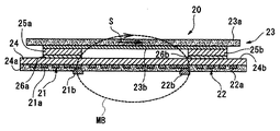
図2は、本発明の磁気デバイスの他の一例を示す斜視図である。また、図3は、図2のA−A線における断面図である。磁気デバイス20は、基板24の一面(下面)24aに形成された第一磁界印加手段21および第二磁界印加手段22と、基板24の他面(上面)24bに配された磁気センサ23とを有する。基板24は、絶縁性の樹脂などから構成されていれば良い。
FIG. 2 is a perspective view showing another example of the magnetic device of the present invention. 3 is a cross-sectional view taken along line AA in FIG. The
第一磁界印加手段21および第二磁界印加手段22は、例えば、金属などの導電膜を基板24の一面24aに沿って平面状に広がるように形成したスパイラルコイル21a,22aであればよい。そして、それぞれのスパイラルコイル21a,22aの巻き方向は、互いに逆向きになるように形成され、かつ、それぞれのスパイラルコイル21a,22aの一端どうしは電気的に接続されている。
The first magnetic field applying means 21 and the second magnetic field applying means 22 may be
こうした構成によって、スパイラルコイル21a,22aの端子21b,22bの間に電流を流すことによって、第一磁界印加手段21および第二磁界印加手段22は、互いに逆向きの磁界を発生させる。そして、第一磁界印加手段21および第二磁界印加手段22の間には、一方向に流れる略環状の一連の磁束からなるバイアス磁界MBが形成される。
With such a configuration, the first magnetic
磁気センサ23は、例えば、絶縁体23aの一面に軟磁性膜23bを形成したものであれば良い。こうした軟磁性膜23bは、例えばメアンダ形状(つづら折り形状)に形成され、その長手方向が感磁方向Sとされる。こうした構成の磁気センサ23は、第一磁界印加手段21および第二磁界印加手段22によって形成されるバイアス磁界MBをなす略環状の磁束の向きに感磁方向Sが沿うように配される。これにより、磁気センサ23には、感磁方向Sに沿ったバイアス磁界MBが印加され、感磁方向Sの磁界強度を高精度に検出可能となる。
The
磁気センサ23と基板24の他面24bとの間には、磁性体25a,25bがそれぞれ配される。こうした磁性体25a,25bは、スパイラルコイル21a,22aの外側領域に重ねて配されていれば良い。磁性体25a,25bによってスパイラルコイル21a,22aの外側領域を覆うことによって、それぞれのスパイラルコイル21a,22aの中心付近から内側に位置するように配された磁気センサ23に対して、スパイラルコイル21a,22aで生じたバイアス磁界MB以外の余分な漏れ磁界の影響を遮断することができる。また、磁気センサ23と基板24の他面24bとの間には、磁気センサ23の軟磁性膜23bに電気的に接続される電極26a,26bが形成されていても良い。
以上のような構成の磁気デバイス20は、2つの磁界印加手段である第一磁界印加手段21および第二磁界印加手段22によって、略環状の一連の磁束からなるバイアス磁界MBを形成でき、このバイアス磁界MBの磁束の向きに沿って磁気センサ23の感磁方向Sを揃えることによって、感磁方向Sの磁界強度を高精度に検出可能となる。
The
そして、このような第一磁界印加手段21および第二磁界印加手段22を基板24に沿った平面状に広がるスパイラルコイル21a,22aから構成することによって、磁気デバイス20全体を小型化、薄型化することができる。さらに、磁性体25a,25bによってスパイラルコイル21a,22aの外側領域を覆うことによって、磁気センサ23に対して、スパイラルコイル21a,22aで生じたバイアス磁界MB以外の余分な漏れ磁界の影響を遮断することができ、磁気センサ23の磁界検出精度をより一層高めることが可能になる。
Then, the first magnetic
2つの磁界印加手段は、互いの位置や磁界発生力を変えることによって、発生させるバイアス磁界をなす磁束の方向を偏向させたりすることもできる。図4(a)では第一磁界印加手段31および第二磁界印加手段32を、基板33の一面に沿って同一平面上に、互いに同じ巻き数のスパイラルコイルから構成している。これにより、基板33に対して均等でほぼ円形の一連の磁束からなるバイアス磁界を発生させることができる。
The two magnetic field applying means can also deflect the direction of the magnetic flux forming the bias magnetic field to be generated by changing the mutual position and magnetic field generating force. In FIG. 4A, the first magnetic
一方、図4(b)では第一磁界印加手段41および第二磁界印加手段42を、段差のある基板43の一面に沿って、互いに異なる平面上にずらして配している。これにより、基板43に対して偏向した楕円形の磁束からなるバイアス磁界を発生させることができる。また、図4(c)では第一磁界印加手段51および第二磁界印加手段52を、互いに異なる巻き数のスパイラルコイルから構成している。これにより、磁束密度が変化した磁束からなるバイアス磁界を発生させることができる。
On the other hand, in FIG. 4B, the first magnetic
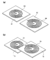
2つの磁界印加手段は、それぞれ別な基板に形成し、電気的に接続されない構成であっても良い。図5(a)では、第一基板61にスパイラルコイルからなる第一磁界印加手段63を、第二基板62にスパイラルコイルからなる第二磁界印加手段64をそれぞれ配した。これによって、第一基板61と第二基板62とを別々に製造して組み合わせることができ、製造が容易になる。また、第一磁界印加手段63と第二磁界印加手段64との間隔を自在に調整して、発生させるバイアス磁界をなす磁束の流れを調節することができる。
The two magnetic field applying units may be formed on different substrates and not electrically connected. In FIG. 5A, a first magnetic
また、図5(b)では、第一基板71と第二基板72のそれぞれにスパイラルコイルからなる第一磁界印加手段73、第二磁界印加手段74をそれぞれ配し、かつ、第一基板71と第二基板72とを互いにずらすことよって、第一磁界印加手段73と第二磁界印加手段74とが互いに異なる面に配される。これにより、第一磁界印加手段73と第二磁界印加手段74とを、互いの位置が自在にレイアウトすることができ、磁気デバイスの設計上の自由度が増す。
In FIG. 5B, a first magnetic
10 磁気デバイス、11 第一磁界印加手段、12 第二磁界印加手段、13 磁気センサ、21a,22a スパイラルコイル、25a,25b 磁性体。
DESCRIPTION OF
Claims (4)
前記第一磁界印加手段と前記第二磁界印加手段は、1つの環状をなすバイアス磁界を形成し、前記磁気センサは、その感磁方向が前記バイアス磁界の方向に沿うように配したことを特徴とする磁気デバイス。 A magnetic device comprising at least a first magnetic field applying means, a second magnetic field applying means, and a magnetic sensor,
The first magnetic field applying unit and the second magnetic field applying unit form one annular bias magnetic field, and the magnetic sensor is arranged so that a magnetic sensitive direction thereof is along a direction of the bias magnetic field. And magnetic device.
The magnetic device according to claim 1, wherein the first magnetic field applying unit and the second magnetic field applying unit are spiral coils having a planar shape.
Priority Applications (1)
| Application Number | Priority Date | Filing Date | Title |
|---|---|---|---|
| JP2006136320A JP2007309671A (en) | 2006-05-16 | 2006-05-16 | Magnetic device |
Applications Claiming Priority (1)
| Application Number | Priority Date | Filing Date | Title |
|---|---|---|---|
| JP2006136320A JP2007309671A (en) | 2006-05-16 | 2006-05-16 | Magnetic device |
Publications (1)
| Publication Number | Publication Date |
|---|---|
| JP2007309671A true JP2007309671A (en) | 2007-11-29 |
Family
ID=38842676
Family Applications (1)
| Application Number | Title | Priority Date | Filing Date |
|---|---|---|---|
| JP2006136320A Withdrawn JP2007309671A (en) | 2006-05-16 | 2006-05-16 | Magnetic device |
Country Status (1)
| Country | Link |
|---|---|
| JP (1) | JP2007309671A (en) |
Cited By (2)
| Publication number | Priority date | Publication date | Assignee | Title |
|---|---|---|---|---|
| JP2018066651A (en) * | 2016-10-19 | 2018-04-26 | Tdk株式会社 | Magnetic sensor inductance element and current sensor having the same |
| JPWO2018143122A1 (en) * | 2017-02-02 | 2019-06-27 | アルプスアルパイン株式会社 | Balanced current sensor |
-
2006
- 2006-05-16 JP JP2006136320A patent/JP2007309671A/en not_active Withdrawn
Cited By (4)
| Publication number | Priority date | Publication date | Assignee | Title |
|---|---|---|---|---|
| JP2018066651A (en) * | 2016-10-19 | 2018-04-26 | Tdk株式会社 | Magnetic sensor inductance element and current sensor having the same |
| JPWO2018143122A1 (en) * | 2017-02-02 | 2019-06-27 | アルプスアルパイン株式会社 | Balanced current sensor |
| CN110235003A (en) * | 2017-02-02 | 2019-09-13 | 阿尔卑斯阿尔派株式会社 | Balanced type current sensor |
| CN110235003B (en) * | 2017-02-02 | 2022-04-01 | 阿尔卑斯阿尔派株式会社 | Balanced current sensor |
Similar Documents
| Publication | Publication Date | Title |
|---|---|---|
| US9651636B2 (en) | Single-chip three-axis magnetic field sensing device | |
| WO2019167598A1 (en) | Magnetic sensor | |
| JP2009300150A (en) | Magnetic sensor and magnetic sensor module | |
| JP2007303860A (en) | Magnetic device | |
| US9488701B2 (en) | Integrated magnatoresistive sensing device | |
| JP6699635B2 (en) | Magnetic sensor | |
| JP5373580B2 (en) | Position detection device | |
| US9128141B2 (en) | Magnatoresistive sensing device and method for fabricating the same | |
| WO2017209169A1 (en) | Magnetic sensor | |
| JP2007309671A (en) | Magnetic device | |
| JP2016145745A (en) | Magnetic sensor | |
| US8395383B2 (en) | Current sensor including magnetic detecting element | |
| CN108780130B (en) | Magnetic sensor | |
| WO2017199787A1 (en) | Magnetic sensor | |
| JP2017040628A (en) | Magnetic sensor | |
| JP2008197002A (en) | Magnetic sensor | |
| JP2007292692A (en) | Magnetic device | |
| JP2019211385A (en) | Magnetic detection device and magnetic bias device | |
| JP2017049010A (en) | Electromagnetic field probe | |
| JP5139822B2 (en) | Magnetic field probe | |
| JP2016206006A (en) | Magnetic sensor | |
| JP2019052891A (en) | Magnetic sensor | |
| JP5373581B2 (en) | Position detection device | |
| CN116609712A (en) | Magnetic sensor | |
| JP2017083280A (en) | Semiconductor device and magnetic sensor device |
Legal Events
| Date | Code | Title | Description |
|---|---|---|---|
| A300 | Application deemed to be withdrawn because no request for examination was validly filed |
Free format text: JAPANESE INTERMEDIATE CODE: A300 Effective date: 20090804 |