JP2007285779A - Calibration circuit, calibration and testing device - Google Patents
Calibration circuit, calibration and testing device Download PDFInfo
- Publication number
- JP2007285779A JP2007285779A JP2006111311A JP2006111311A JP2007285779A JP 2007285779 A JP2007285779 A JP 2007285779A JP 2006111311 A JP2006111311 A JP 2006111311A JP 2006111311 A JP2006111311 A JP 2006111311A JP 2007285779 A JP2007285779 A JP 2007285779A
- Authority
- JP
- Japan
- Prior art keywords
- waveform
- terminal
- measuring device
- level
- generator
- Prior art date
- Legal status (The legal status is an assumption and is not a legal conclusion. Google has not performed a legal analysis and makes no representation as to the accuracy of the status listed.)
- Granted
Links
Images
Landscapes
- Tests Of Electronic Circuits (AREA)
Abstract
Description
本発明は、キャリブレーション回路、キャリブレーション方法、及び試験装置に関する。特に本発明は、波形発生器と波形測定器とを備える装置をキャリブレーションするキャリブレーション回路及びキャリブレーション方法、並びに波形発生器と波形測定器とを備える試験装置に関する。 The present invention relates to a calibration circuit, a calibration method, and a test apparatus. In particular, the present invention relates to a calibration circuit and calibration method for calibrating an apparatus including a waveform generator and a waveform measuring instrument, and a test apparatus including a waveform generator and a waveform measuring instrument.
半導体装置等の被試験デバイスのAC特性を試験する試験装置は、被試験デバイスに対して供給するアナログの信号を発生する波形発生器と、被試験デバイスからのアナログの出力信号を取得する波形測定器とを備える。波形発生器および波形測定器は、出力レベルの誤差および測定レベルの誤差が小さいことが望ましい。また、試験装置が複数の波形発生部および複数の波形測定器を備える場合には、これら複数の波形発生部および複数の波形測定器は、スキューが小さいことが望ましい。 A test apparatus for testing AC characteristics of a device under test such as a semiconductor device includes a waveform generator that generates an analog signal supplied to the device under test, and a waveform measurement that acquires an analog output signal from the device under test With a vessel. It is desirable that the waveform generator and the waveform measuring instrument have a small output level error and measurement level error. Further, when the test apparatus includes a plurality of waveform generation units and a plurality of waveform measurement devices, it is desirable that the plurality of waveform generation units and the plurality of waveform measurement devices have small skew.
なお、現時点で先行技術文献の存在を認識していないので、先行技術文献に関する記載を省略する。 In addition, since the presence of a prior art document is not recognized at this time, the description regarding a prior art document is abbreviate | omitted.
ところで、このような試験装置は、外部測定機器であるオシロスコープ、信号発生器およびレベル測定器を接続して、出力レベルの誤差、測定レベルの誤差およびスキューの測定を目的としたキャリブレーションが行われる。しかしながら、このような外部測定機器を接続したキャリブレーション処理は、接続が複雑となり、この結果、処理時間が長く、コストも高くなる。 By the way, in such a test apparatus, an oscilloscope, a signal generator, and a level measuring instrument, which are external measuring devices, are connected to perform calibration for the purpose of measuring an output level error, a measurement level error, and a skew. . However, the calibration process in which such an external measuring device is connected becomes complicated, resulting in a long processing time and high cost.
そこで本発明は、上記の課題を解決することのできるキャリブレーション回路、キャリブレーション方法、及び試験装置を提供することを目的とする。この目的は特許請求の範囲における独立項に記載の特徴の組み合わせにより達成される。また従属項は本発明の更なる有利な具体例を規定する。 Accordingly, an object of the present invention is to provide a calibration circuit, a calibration method, and a test apparatus that can solve the above-described problems. This object is achieved by a combination of features described in the independent claims. The dependent claims define further advantageous specific examples of the present invention.
上記課題を解決するために、本発明の第1形態においては、第1及び第2の波形発生器と、第1及び第2の波形発生器に対応して設けられた第1及び第2の波形測定器とを備える装置をキャリブレーションするキャリブレーション回路であって、第1及び第2の波形発生器、並びに第1及び第2の波形測定器に対応して設けられ、第1及び第2の波形発生器の出力端、並びに第1及び第2の波形測定器の入力端のそれぞれを、第1の端子又は第2の端子のいずれに接続するかを切り替える第1から第4のスイッチと、第1のスイッチの第2の端子を、第3のスイッチ及び第4のスイッチの双方の第2の端子に接続する分配経路と、第1のスイッチの第1の端子と、第3のスイッチの第1の端子とを接続する第1の接続経路と、第2のスイッチの第1の端子と、第4のスイッチの第1の端子とを接続する第2の接続経路とを備えるキャリブレーション回路を提供する。 In order to solve the above problems, in the first embodiment of the present invention, the first and second waveform generators and the first and second waveform generators provided corresponding to the first and second waveform generators are provided. A calibration circuit for calibrating a device including a waveform measuring device, which is provided corresponding to the first and second waveform generators and the first and second waveform measuring devices. First to fourth switches for switching whether the output terminal of the first waveform generator and the input terminals of the first and second waveform measuring devices are connected to the first terminal or the second terminal, respectively. A distribution path for connecting the second terminal of the first switch to the second terminals of both the third switch and the fourth switch, the first terminal of the first switch, and the third switch A first connection path for connecting the first terminal of the second switch and a second switch Providing a first terminal, a calibration circuit and a second connection path connecting the first terminal of the fourth switch.
分配経路、第1の接続経路、及び第2の接続経路における伝搬遅延時間は、略等しくてよい。分配経路は、第1のスイッチの第2の端子に接続される第1の抵抗と、第1の抵抗と、第3のスイッチの第2の端子との間に接続され、第1の抵抗と略同一の抵抗値を有する第2の抵抗と、第1の抵抗と、第4のスイッチの第2の端子との間に接続され、第1の抵抗と略同一の抵抗値を有する第3の抵抗とを有してよい。
キャリブレーション回路は、与えられる信号のレベルを測定するレベル測定器と、第2のスイッチの第2の端子と、レベル測定器とを接続する測定経路とを更に備えてよい。
The propagation delay times in the distribution path, the first connection path, and the second connection path may be substantially equal. The distribution path is connected between the first resistor connected to the second terminal of the first switch, the first resistor, and the second terminal of the third switch, and the first resistor A second resistor having substantially the same resistance value, a first resistor, and a third resistor connected between the second terminal of the fourth switch and having substantially the same resistance value as the first resistor. Resistance.
The calibration circuit may further include a level measuring device that measures the level of a given signal, a second terminal of the second switch, and a measurement path that connects the level measuring device.
キャリブレーション回路は、第1から第4のスイッチに対して、それぞれ対応する機器を第2の端子に接続させた状態で、第1の波形発生器に所定の信号を出力させ、第1の波形測定器及び第2の波形測定器が所定の信号を受け取るそれぞれのタイミングに基づいて、第1の波形測定器と第2の波形測定器との間のスキューを算出する測定器スキュー算出部を更に備えてよい。
キャリブレーション回路は、第1から第4のスイッチに対して、それぞれ対応する機器を第1の端子に接続させた状態で、第1の波形発生器及び第2の波形発生器に所定の信号を出力させ、第1の波形測定器及び第2の波形測定器が、それぞれ対応する波形発生器から所定の信号を受け取るタイミングを検出し、当該タイミング及び測定器スキュー算出部が算出したスキューに基づいて、第1の波形発生器と第2の波形発生器との間のスキューを算出する発生器スキュー算出部を更に備えてよい。
The calibration circuit causes the first waveform generator to output a predetermined signal in a state where the corresponding devices are connected to the second terminal for the first to fourth switches, and the first waveform A measuring instrument skew calculating section for calculating a skew between the first waveform measuring instrument and the second waveform measuring instrument based on respective timings at which the measuring instrument and the second waveform measuring instrument receive a predetermined signal; You may be prepared.
The calibration circuit sends predetermined signals to the first waveform generator and the second waveform generator in a state where the corresponding devices are connected to the first terminals for the first to fourth switches, respectively. The first waveform measuring device and the second waveform measuring device detect the timing at which the predetermined signal is received from the corresponding waveform generator, and based on the timing and the skew calculated by the measuring device skew calculation unit A generator skew calculation unit for calculating a skew between the first waveform generator and the second waveform generator may be further provided.
キャリブレーション回路は、第1から第4のスイッチに対して、それぞれ対応する機器を第2の端子に接続させた状態で、第2の波形発生器に所定の信号を出力させ、レベル測定器に所定の信号のレベルを測定させる基準レベル測定部と、第1から第4のスイッチに対して、それぞれ対応する機器を第1の端子に接続させた状態で、第2の波形発生器に所定の信号を出力させ、第2の波形測定器が測定する所定の信号のレベルと、基準レベル測定部が測定した所定の信号のレベルとに基づいて、第2の波形測定器の測定誤差を算出するレベル測定誤差算出部と
を更に備えてよい。
レベル測定誤差算出部は更に、第1から第4のスイッチに対して、それぞれ対応する機器を第2の端子に接続させた状態で、第1の波形発生器に所定の信号を出力させ、第1の波形測定器及び第2の波形測定器における測定結果の差分に基づいて、第1の波形測定器の測定誤差を算出してよい。
The calibration circuit outputs a predetermined signal to the second waveform generator in a state where the corresponding devices are connected to the second terminals for the first to fourth switches, and causes the level measuring device to With the reference level measuring unit for measuring the level of the predetermined signal and the first to fourth switches, corresponding devices are connected to the first terminal, and the second waveform generator is set to the predetermined level. A signal is output, and a measurement error of the second waveform measuring device is calculated based on the level of the predetermined signal measured by the second waveform measuring device and the level of the predetermined signal measured by the reference level measuring unit. And a level measurement error calculation unit.
The level measurement error calculation unit further causes the first waveform generator to output a predetermined signal in a state where the corresponding devices are connected to the second terminals for the first to fourth switches, respectively. The measurement error of the first waveform measuring instrument may be calculated based on the difference between the measurement results of the first waveform measuring instrument and the second waveform measuring instrument.
キャリブレーション回路は、第1から第4のスイッチに対して、それぞれ対応する機器を第1の端子に接続させた状態で、第1の波形発生器及び第2の波形発生器に略同一のレベル設定の信号を出力させ、第1の波形測定器及び第2の波形測定器におけるレベル測定結果の差分を検出し、当該レベル測定結果の差分、第1の波形発生器の測定誤差、及び第2の波形発生器の測定誤差に基づいて、第1の波形測定器及び第2の波形測定器が出力する信号のレベル誤差を算出する出力レベル算出部を更に備えてよい。 The calibration circuit has substantially the same level as the first waveform generator and the second waveform generator with the corresponding devices connected to the first terminal for the first to fourth switches, respectively. A setting signal is output to detect a difference between the level measurement results in the first waveform measuring instrument and the second waveform measuring instrument, and the difference between the level measurement results, the measurement error of the first waveform generator, and the second An output level calculating unit that calculates a level error of signals output from the first waveform measuring device and the second waveform measuring device may be further provided based on the measurement error of the waveform generator.
キャリブレーション回路は、第1から第4のスイッチに対して、それぞれ対応する機器を第2の端子及び第1の端子に交互に接続させるスイッチ制御部を更に備え、測定器スキュー算出部及び基準レベル測定部は、第1から第4のスイッチが、それぞれ対応する機器を第2の端子に接続した場合に、第1の波形測定器と第2の波形測定器との間のスキューと、レベル測定器における所定の信号のレベルの測定結果とを並行して検出してよい。 The calibration circuit further includes a switch control unit that alternately connects corresponding devices to the second terminal and the first terminal with respect to the first to fourth switches, and includes a measuring instrument skew calculation unit and a reference level. When the first to fourth switches connect the corresponding devices to the second terminal, the measurement unit measures the skew and level between the first waveform measuring instrument and the second waveform measuring instrument. The measurement result of the level of the predetermined signal in the instrument may be detected in parallel.
発生器スキュー算出部及びレベル測定誤差算出部は、第1から第4のスイッチが、それぞれ対応する機器を第1の端子に接続した場合に、第1の波形発生器と第2の波形発生器との間のスキューと、第2の波形測定器の測定誤差とを並行して検出してよい。
発生器スキュー算出部及び出力レベル算出部は、第1から第4のスイッチが、それぞれ対応する機器を第1の端子に接続した場合に、第1の波形発生器及び第2の波形発生器の間のスキューと、第1の波形測定器及び第2の波形測定器が出力する信号のレベル誤差とを並行して検出してよい。
The generator skew calculation unit and the level measurement error calculation unit are configured such that the first waveform generator and the second waveform generator when the first to fourth switches connect the corresponding devices to the first terminal, respectively. And the measurement error of the second waveform measuring device may be detected in parallel.
The generator skew calculation unit and the output level calculation unit are configured so that the first waveform generator and the output level calculation unit are connected to the first waveform generator and the second waveform generator when the corresponding devices are connected to the first terminal. The skew between them and the level error of the signals output from the first waveform measuring device and the second waveform measuring device may be detected in parallel.
本発明の第2形態においては、第1及び第2の波形発生器と、第1の波形発生器に対応する第1の波形測定器と、第2の波形発生器に対応する第2の波形測定器とを備える装置を、請求項1に記載のキャリブレーション回路を用いてキャリブレーションするキャリブレーション方法であって、第1から第4のスイッチに対して、それぞれ対応する機器を第2の端子に接続させる第1のスイッチ制御段階と、第1の波形発生器に所定の信号を出力させ、第1の波形測定器及び第2の波形測定器が所定の信号を受け取るそれぞれのタイミングを検出する測定タイミング検出段階と、測定タイミング検出段階において検出したタイミングに基づいて、第1の波形測定器と第2の波形測定器との間のスキューを算出する測定器スキュー算出段階と、第1から第4のスイッチに対して、それぞれ対応する機器を第1の端子に接続させる第2のスイッチ制御段階と、第1の波形発生器及び第2の波形発生器に所定の信号を出力させ、第1の波形測定器及び第2の波形測定器が、それぞれ対応する波形発生器から所定の信号を受け取るタイミングを検出する出力タイミング検出段階と、出力タイミング検出段階において検出したタイミング及び測定器スキュー算出段階において算出したスキューに基づいて、第1の波形発生器と第2の波形発生器との間のスキューを算出する発生器スキュー算出段階とを備えるキャリブレーション方法を提供する。 In the second embodiment of the present invention, the first and second waveform generators, the first waveform measuring device corresponding to the first waveform generator, and the second waveform corresponding to the second waveform generator. A calibration method for calibrating a device including a measuring device using the calibration circuit according to claim 1, wherein corresponding devices are respectively connected to a second terminal with respect to the first to fourth switches. A first switch control stage to be connected to the first waveform generator, and a first waveform generator to output a predetermined signal to detect timings at which the first waveform measuring instrument and the second waveform measuring instrument receive the predetermined signal, respectively. A measurement timing detecting stage, a measuring instrument skew calculating stage for calculating a skew between the first waveform measuring instrument and the second waveform measuring instrument based on the timing detected in the measuring timing detecting stage; To the fourth switch, the second switch control stage for connecting the corresponding device to the first terminal, the first waveform generator and the second waveform generator to output a predetermined signal, An output timing detection stage in which the first waveform measuring instrument and the second waveform measuring instrument each receive a predetermined signal from the corresponding waveform generator, and timing detected in the output timing detection stage and calculation of the instrument skew A calibration method is provided that includes a generator skew calculation step of calculating a skew between a first waveform generator and a second waveform generator based on the skew calculated in the step.
本発明の第3形態においては、被試験デバイスを試験する試験装置であって、被試験デバイスに対して並列に供給する第1及び第2の試験信号を生成する第1及び第2の波形発生器と、被試験デバイスが並列に出力する第1及び第2の出力信号を測定する第1及び第2の波形測定器と、第1及び第2の波形発生器、並びに第1及び第2の波形測定器をキャリブレーションするキャリブレーション回路とを備え、キャリブレーション回路は、第1及び第2の波形発生器、並びに第1及び第2の波形測定器に対応して設けられ、第1及び第2の波形発生器の出力端、並びに第1及び第2の波形測定器の入力端のそれぞれを、第1の端子又は第2の端子のいずれに接続するかを切り替える第1から第4のスイッチと、第1のスイッチの第2の端子を、第3のスイッチ及び第4のスイッチの双方の第2の端子に接続する分配経路と、第1のスイッチの第1の端子と、第3のスイッチの第1の端子とを接続する第1の接続経路と、第2のスイッチの第1の端子と、第4のスイッチの第1の端子とを接続する第2の接続経路とを有する試験装置を提供する。 According to a third aspect of the present invention, there is provided a test apparatus for testing a device under test, which generates first and second waveforms for generating first and second test signals supplied in parallel to the device under test. , First and second waveform measuring devices for measuring first and second output signals output in parallel by the device under test, first and second waveform generators, and first and second A calibration circuit that calibrates the waveform measuring instrument, the calibration circuit being provided corresponding to the first and second waveform generators and the first and second waveform measuring instruments, First to fourth switches for switching whether the output terminal of the two waveform generators and the input terminals of the first and second waveform measuring devices are connected to the first terminal or the second terminal, respectively. And the second terminal of the first switch A distribution path connected to the second terminals of both the third switch and the fourth switch, a first terminal of the first switch, and a first terminal connecting the first terminal of the third switch A test apparatus is provided that includes a connection path, a first terminal of a second switch, and a second connection path that connects the first terminal of a fourth switch.
なお、上記の発明の概要は、本発明の必要な特徴の全てを列挙したものではなく、これらの特徴群のサブコンビネーションもまた、発明となりうる。 The above summary of the invention does not enumerate all the necessary features of the present invention, and sub-combinations of these feature groups can also be the invention.
本発明によれば、簡易な構成によりキャリブレーションをすることができる。 According to the present invention, calibration can be performed with a simple configuration.
以下、発明の実施の形態を通じて本発明を説明するが、以下の実施形態は特許請求の範囲にかかる発明を限定するものではなく、また実施形態の中で説明されている特徴の組み合わせの全てが発明の解決手段に必須であるとは限らない。 Hereinafter, the present invention will be described through embodiments of the invention. However, the following embodiments do not limit the invention according to the scope of claims, and all combinations of features described in the embodiments are included. It is not necessarily essential for the solution of the invention.
図1は、本実施形態に係る試験装置100の構成を示す。試験装置100は、被試験デバイスを試験する。試験装置100は、試験装置本体部10と、キャリブレーション回路30とを備える。試験装置本体部10は、被試験デバイスに対して並列に供給する第1及び第2の試験信号を生成する第1の波形発生器11及び第2の波形発生器12と、被試験デバイスが並列に出力する第1及び第2の出力信号を測定する第1の波形測定器21及び第2の波形測定器22とを有する。キャリブレーション回路30は、第1の波形発生器11及び第2の波形発生器12並びに第1の波形測定器21及び第1の波形測定器21をキャリブレーションする。キャリブレーション回路30は、一例として、第1の波形発生器11及び第2の波形発生器12の出力信号のレベル誤差、第1の波形測定器21及び第2の波形測定器22の測定レベルの測定誤差、第1の波形発生器11と第2の波形発生器12との間のスキュー及び第1の波形測定器21と第2の波形測定器22との間のスキューを測定する。また、キャリブレーション回路30は、一例として、パフォーマンスボード上に形成されて試験装置本体部10に取り付けられてよい。
FIG. 1 shows a configuration of a
図2は、本実施形態に係るキャリブレーション回路30の構成を示す。キャリブレーション回路30は、第1のスイッチ41と、第2のスイッチ42と、第3のスイッチ43と、第4のスイッチ44と、第1の接続経路51と、第2の接続経路52と、分配経路53と、レベル測定器54と、測定経路55とを有する。
FIG. 2 shows a configuration of the
第1から第4のスイッチ41〜44は、第1及び第2の波形発生器11、12、並びに第1及び第2の波形測定器21、22に対応して設けられ、第1及び第2の波形発生器11、12の出力端、並びに第1及び第2の波形測定器21、22の入力端のそれぞれを、第1の端子又は第2の端子のいずれに接続するかを切り替える。より詳細には、第1のスイッチ41は、第1の波形発生器11の出力端を、第1の端子411又は第2の端子412のいずれに接続するかを切り換える。第2のスイッチ42は、第2の波形発生器12の出力端を、第1の端子421又は第2の端子422のいずれに接続するかを切り換える。第3のスイッチ43は、第1の波形測定器21の入力端を、第1の端子431又は第2の端子432のいずれに接続するかを切り換える。第4のスイッチ44は、第2の波形測定器22の入力端を、第1の端子441又は第2の端子442のいずれに接続するかを切り換える。
The first to
第1の接続経路51は、第1のスイッチ41の第1の端子411と、第3のスイッチ43の第1の端子431とを接続する。第2の接続経路52は、第2のスイッチ42の第1の端子421と、第4のスイッチ44の第1の端子441とを接続する。なお、第1の接続経路51および第2の接続経路52における伝播遅延時間は、略等しい。
The
分配経路53は、第1のスイッチ41の第2の端子412を、第3のスイッチ43及び第4のスイッチ44の双方の第2の端子432、442に接続する。分配経路53は、一例として、第1の抵抗61と、第2の抵抗62と、第3の抵抗63とを含んでよい。第1の抵抗61は、一端が第1のスイッチ41の第2の端子412に接続される。第2の抵抗62は、第1のスイッチ41の第2の端子412が接続されていない第1の抵抗61の他端と、第3のスイッチ43の第2の端子432との間に接続され、第1の抵抗61と略同一の抵抗値を有する。第3の抵抗63は、第1のスイッチ41の第2の端子412が接続されていない第1の抵抗61の他端と、第4のスイッチ44の第2の端子442との間に接続され、61と略同一の抵抗値を有する。このような構成の分配経路53によれば、第1のスイッチ41の第2の端子412を介して入力する信号を、第3のスイッチ43の第2の端子432および第4のスイッチ44の第2の端子442の両者へ、インピーダンス整合を保って出力する分配器として機能する。なお、分配経路53における伝播遅延時間は、第1の接続経路51及び第2の接続経路52における伝播遅延時間と略等しい。
The
レベル測定器54は、与えられる信号のレベルを測定する。レベル測定器54は、一例として、標準器により確度が補償されている。測定経路55は、第2のスイッチ42の第2の端子422と、レベル測定器54の入力端とを接続する。なお、測定経路55における伝播遅延時間は、第1の接続経路51及び第2の接続経路52における伝播遅延時間と略等しくてよい。
The
スイッチ制御部71は、第1から第4のスイッチ41〜44に対して、それぞれ対応する機器を第1の端子及び第2の端子に接続させる。スイッチ制御部71は、測定器スキュー算出部81、発生器スキュー算出部82、基準レベル測定部83、レベル測定誤差算出部84又は出力レベル算出部85の制御に応じて、第1から第4のスイッチ41〜44が対応する機器を接続する端子を、交互に切り換える。スイッチ制御部71は、第1から第4のスイッチ41〜44を共通の信号により制御してよい。共通の信号により制御された第1から第4のスイッチ41〜44は、それぞれ対応する機器を同じ端子側に接続する。
The
このようなスイッチ制御部71によれば、第1から第4のスイッチ41〜44を第1の端子側に切り換えることにより、第1の波形発生器11により出力された信号を第1の接続経路51を介して第1の波形測定器21に供給し、第2の波形発生器12により出力された信号を第2の接続経路52を介して第2の波形測定器22に供給することができる。また、スイッチ制御部71によれば、第1から第4のスイッチ41〜44を第2の端子側に切り換えることにより、第1の波形発生器11により出力された信号を分配経路53を介して第1の波形測定器21及び第2の波形測定器22に均等に分配して供給し、第2の波形発生器12により出力された信号を測定経路55を介してレベル測定器54に供給することができる。
According to such a
測定器スキュー算出部81は、第1の波形測定器21と第2の波形測定器22との間のスキューを算出する。発生器スキュー算出部82は、第1の波形発生器11と第2の波形発生器12との間のスキューを算出する。基準レベル測定部83は、第2の波形発生器12から出力された所定の信号のレベルをレベル測定器54に測定させる。レベル測定誤差算出部84は、第1の波形測定器21および第2の波形測定器22の信号レベルの測定誤差を算出する。出力レベル算出部85は、第1の波形発生器11及び第2の波形発生器12が出力する信号のレベル誤差を算出する。
The measuring instrument
以上のようなキャリブレーション回路30によれば、簡易な構成および制御により、第1の波形発生器11と第2の波形発生器12との間のスキュー、第1の波形測定器21と第2の波形測定器22との間のスキュー、第1の波形発生器11及び第2の波形発生器12のレベル誤差、第1の波形測定器21及び第2の波形測定器22の測定誤差を測定することができる。この結果、キャリブレーション回路30によれば、これらの測定時間を短くでき、コストも下げることができる。
According to the
図3は、第1の波形測定器21及び第2の波形測定器22の間のスキューの算出時における、第1の波形発生器11、第2の波形発生器12、第1の波形測定器21、第2の波形測定器22及びキャリブレーション回路30の接続関係を示す。第1の波形測定器21及び第2の波形測定器22の間のスキューを算出する場合、測定器スキュー算出部81は、第1から第4のスイッチ41〜44に対して、それぞれ対応する機器を第2の端子412、422、432、442に接続させた状態とする。すなわち、測定器スキュー算出部81は、第1の波形発生器11の出力端と第1の波形測定器21の入力端とを分配経路53を介して接続させ、第1の波形発生器11の出力端と第2の波形測定器22の入力端とを分配経路53を介して接続させる。この接続状態において、測定器スキュー算出部81は、第1の波形発生器11に所定の信号を出力させる。この結果、第1の波形測定器21および第2の波形測定器22は、第1の波形発生器11により出力された所定の信号を入力する。
FIG. 3 shows the
そして、測定器スキュー算出部81は、第1の波形測定器21及び第2の波形測定器22が所定の信号を受け取るそれぞれのタイミングに基づいて、第1の波形測定器21と第2の波形測定器22との間のスキューを算出する。測定器スキュー算出部81は、一例として、第1の波形測定器21および第2の波形測定器22が受け取った信号を周波数解析し、周波数毎に位相差を検出してスキューを算出してよい。キャリブレーション回路30によれば、以上のような簡易な構成及び制御により、第1の波形測定器21と第2の波形測定器22との間のスキューを算出することができる。
Then, the measuring instrument
図4は、第1の波形発生器11及び第2の波形発生器12の間のスキューの算出時における、第1の波形発生器11、第2の波形発生器12、第1の波形測定器21、第2の波形測定器22及びキャリブレーション回路30の接続関係を示す。キャリブレーション回路30は、図3で説明した第1の波形測定器21及び第2の波形測定器22の間のスキューの算出処理の後に、第1の波形発生器11及び第2の波形発生器12の間のスキューを算出する。第1の波形発生器11及び第2の波形発生器12の間のスキューを算出する場合、発生器スキュー算出部82は、第1から第4のスイッチ41〜44に対して、それぞれ対応する機器を第1の端子411、421、431、441に接続させた状態とする。すなわち、発生器スキュー算出部82は、第1の波形発生器11の出力端と第1の波形測定器21の入力端とを第1の接続経路51を介して接続させ、第2の波形発生器12の出力端と第2の波形測定器22の入力端とを第2の接続経路52を介して接続させる。この接続状態において、発生器スキュー算出部82は、第1の波形発生器11及び第2の波形発生器12に所定の信号を出力させる。この結果、第1の波形測定器21は、第1の波形発生器11により出力された所定の信号を入力し、第2の波形測定器22は、第2の波形発生器12により出力された所定の信号を入力する。
FIG. 4 shows the
そして、発生器スキュー算出部82は、第1の波形測定器21及び第2の波形測定器22が、それぞれ対応する波形発生器11、12から所定の信号を受け取るタイミングを検出し、当該タイミング及び測定器スキュー算出部81が算出したスキューに基づいて、第1の波形発生器11と第2の波形発生器12との間のスキューを算出する。発生器スキュー算出部82は、一例として、第1の波形測定器21および第2の波形測定器22が受け取った信号を周波数解析して、周波数毎に位相差を検出して、発生器および測定器の合計のスキューを算出する。そして、発生器スキュー算出部82は、算出した合計のスキューから測定器スキュー算出部81が算出したスキューを減算することにより、第1の波形発生器11と第2の波形発生器12との間のスキューを算出してよい。キャリブレーション回路30によれば、以上のような簡易な構成及び制御により、第1の波形発生器11と第2の波形発生器12との間のスキューを算出することができる。
Then, the generator
図5は、第2の波形発生器12の出力信号レベルの測定時における、第1の波形発生器11、第2の波形発生器12、第1の波形測定器21、第2の波形測定器22及びキャリブレーション回路30の接続関係を示す。第2の波形発生器12の出力信号レベルを測定する場合、基準レベル測定部83は、第1から第4のスイッチ41〜44に対して、それぞれ対応する機器を第2の端子412、422、432、442に接続させた状態とする。すなわち、基準レベル測定部83は、第2の波形発生器12の出力端とレベル測定器54の入力端とを測定経路55を介して接続させる。この接続状態において、基準レベル測定部83は、第2の波形発生器12に所定の信号を出力させる。この結果、レベル測定器54は、第2の波形発生器12により出力された所定の信号を入力する。そして、基準レベル測定部83は、レベル測定器54に所定の信号のレベルを測定させ、レベル測定器54による測定結果を検出する。キャリブレーション回路30によれば、以上のような簡易な構成及び制御により第2の波形発生器12の出力信号のレベルを、所定の確度で測定することができる。
FIG. 5 shows the
なお、測定器スキュー算出部81及び基準レベル測定部83は、第1から第4のスイッチ41〜44が、それぞれ対応する機器を第2の端子412、422、432、442に接続した場合に、第1の波形測定器21と第2の波形測定器22との間のスキューと、レベル測定器54における所定の信号のレベルの測定結果とを並行して検出してよい。これにより、キャリブレーション回路30によれば、第1の波形測定器21と第2の波形測定器22との間のスキューおよび第2の波形発生器12の出力信号のレベルを、効率よく測定することができる。
Note that the measuring instrument
図6は、第2の波形測定器22の測定誤差の算出時における、第1の波形発生器11、第2の波形発生器12、第1の波形測定器21、第2の波形測定器22及びキャリブレーション回路30の接続関係を示す。キャリブレーション回路30は、図5で説明した第2の波形発生器12の出力信号レベルの測定の後に、第2の波形測定器22の測定誤差を測定する。第2の波形測定器22の測定誤差を測定する場合、レベル測定誤差算出部84は、第1から第4のスイッチ41〜44に対して、それぞれ対応する機器を第1の端子411、421、431、441に接続させた状態とする。すなわち、レベル測定誤差算出部84は、第2の波形発生器12の出力端と第2の波形測定器22の入力端とを第2の接続経路52を介して接続させる。この接続状態において、レベル測定誤差算出部84は、第2の波形発生器12に所定の信号を出力させる。この結果、第2の波形測定器22は、第2の波形発生器12により出力された所定の信号を入力する。
FIG. 6 shows the
そして、レベル測定誤差算出部84は、第2の波形測定器22が測定する所定の信号のレベルと、基準レベル測定部83が測定した所定の信号のレベルとに基づいて、第2の波形測定器22の測定誤差を算出する。レベル測定誤差算出部84は、一例として、標準器により確度が補償されたレベル測定器54により測定した所定の信号のレベルと、第2の波形測定器22により測定がされた所定の信号のレベルとの差分に基づき、第2の波形測定器22の測定誤差を算出してよい。キャリブレーション回路30によれば、以上のような簡易な構成及び制御により、第2の波形測定器22のレベルの測定誤差を測定することができる。
Then, the level measurement
なお、発生器スキュー算出部82及びレベル測定誤差算出部84は、第1から第4のスイッチ41〜44が、それぞれ対応する機器を第1の端子411、421、431、441に接続した場合に、第1の波形発生器11と第2の波形発生器12との間のスキューと、第2の波形測定器22の測定誤差とを並行して検出してよい。これにより、キャリブレーション回路30によれば、第1の波形発生器11と第2の波形発生器12との間のスキューおよび第2の波形測定器22の測定誤差を、効率よく測定することができる。
The generator
図7は、第1の波形測定器21の測定誤差の算出時における、第1の波形発生器11、第2の波形発生器12、第1の波形測定器21、第2の波形測定器22及びキャリブレーション回路30の接続関係を示す。キャリブレーション回路30は、図6で説明した第2の波形測定器22の測定誤差の算出の後に、第1の波形測定器21の測定誤差を算出する。第1の波形測定器21の測定誤差を算出する場合、レベル測定誤差算出部84は、第1から第4のスイッチ41〜44に対して、それぞれ対応する機器を第2の端子412、422、432、442に接続させた状態とする。すなわち、レベル測定誤差算出部84は、第1の波形発生器11の出力端と第1の波形測定器21の入力端とを分配経路53を介して接続させ、第1の波形発生器11の出力端と第2の波形測定器22の入力端とを分配経路53を介して接続させる。この接続状態において、レベル測定誤差算出部84は、第1の波形発生器11に所定の信号を出力させる。この結果、第1の波形測定器21および第2の波形測定器22は、第1の波形発生器11により出力された所定の信号を入力する。
FIG. 7 shows the
そして、レベル測定誤差算出部84は、第1の波形測定器21及び第2の波形測定器22における測定結果の差分に基づいて、第1の波形測定器21の測定誤差を算出する。レベル測定誤差算出部84は、一例として、既に算出された第2の波形測定器22の測定誤差に基づき、第2の波形測定器22の測定結果を補償する。そして、レベル測定誤差算出部84は、測定誤差が補償された第2の波形測定器22による測定結果と第2の波形測定器22の測定結果との差分を算出して、第1の波形測定器21の測定誤差を算出してよい。キャリブレーション回路30によれば、以上のような簡易な構成及び制御により、第1の波形測定器21の測定誤差を測定することができる。
Then, the level
図8は、第1の波形発生器11及び第2の波形発生器12のレベル誤差の算出時における、第1の波形発生器11、第2の波形発生器12、第1の波形測定器21、第2の波形測定器22及びキャリブレーション回路30の接続関係を示す。キャリブレーション回路30は、図7で説明した第1の波形測定器21の測定誤差の算出の後に、第1の波形発生器11および第2の波形発生器12のレベル誤差を算出する。第1の波形発生器11および第2の波形発生器12のレベル誤差を算出する場合、出力レベル算出部85は、第1から第4のスイッチ41〜44に対して、それぞれ対応する機器を第1の端子411、421、431、441に接続させた状態とする。すなわち、出力レベル算出部85は、第1の波形発生器11の出力端と第1の波形測定器21の入力端とを第1の接続経路51を介して接続させ、第2の波形発生器12の出力端と第2の波形測定器22の入力端とを第2の接続経路52を介して接続させる。この接続状態において、出力レベル算出部85は、第1の波形発生器11及び第2の波形発生器12に略同一のレベル設定の信号を出力させる。この結果、第1の波形測定器21は、第1の波形発生器11により出力された第2の波形発生器12と略同一のレベル設定の信号を入力し、第2の波形測定器22は、第2の波形発生器12により出力された第1の波形発生器11と略同一のレベル設定の信号を入力する。
FIG. 8 shows the
そして、出力レベル算出部85は、第1の波形測定器21及び第2の波形測定器22におけるレベル測定結果の差分を検出し、当該レベル測定結果の差分、レベル測定誤差算出部84により算出された第1の波形発生器11の測定誤差、及びレベル測定誤差算出部84により算出された第2の波形発生器12の測定誤差に基づいて、第1の波形測定器21及び第2の波形測定器22が出力する信号のレベル誤差を算出する。出力レベル算出部85は、一例として、既に算出された第1の波形測定器21および第2の波形測定器22の測定誤差に基づき、第1の波形測定器21および第2の波形測定器22の測定結果を補償する。そして、出力レベル算出部85は、測定誤差が補償された第1の波形測定器21の測定結果に基づき第1の波形発生器11のレベル誤差を算出し、測定誤差が補償された第2の波形測定器22の測定結果に基づき第2の波形発生器12のレベル誤差を算出してよい。キャリブレーション回路30によれば、以上のような簡易な構成及び制御により、第1の波形発生器11及び第2の波形発生器12のレベル誤差を算出することができる。
Then, the output
発生器スキュー算出部82及び出力レベル算出部85は、第1から第4のスイッチ41〜44が、それぞれ対応する機器を第1の端子411、421、431、441に接続した場合に、第1の波形発生器11及び第2の波形発生器12の間のスキューと、第1の波形測定器21及び第2の波形測定器22が出力する信号のレベル誤差とを並行して検出してよい。これによりキャリブレーション回路30によれば、第1の波形発生器11及び第2の波形発生器12の間のスキュー及び第1の波形測定器21及び第2の波形測定器22が出力する信号のレベル誤差を効率よく測定することができる。
The generator
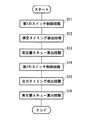
図9は、キャリブレーション回路30によるスキュー算出処理の流れの一例を示す。まず、スイッチ制御部71は、第1から第4のスイッチ41〜44に対して、それぞれ対応する機器を第2の端子412、422、432、442に接続させる(S11:第1のスイッチ制御段階)。次に、測定器スキュー算出部81は、第1の波形発生器11に所定の信号を出力させ、第1の波形測定器21及び第2の波形測定器22が所定の信号を受け取るそれぞれのタイミングを検出する(S12:測定タイミング検出段階)。次に、測定器スキュー算出部81は、測定タイミング検出段階において検出したタイミングに基づいて、第1の波形測定器21と第2の波形測定器22との間のスキューを算出する(測定器スキュー算出段階:S13)。
FIG. 9 shows an example of the flow of skew calculation processing by the
次に、スイッチ制御部71は、第1から第4のスイッチ41〜44に対して、それぞれ対応する機器を第1の端子411、421、431、441に接続させる(S14:第2のスイッチ制御段階)。次に、発生器スキュー算出部82は、第1の波形発生器11及び第2の波形発生器12に所定の信号を出力させ、第1の波形測定器21及び第2の波形測定器22が、それぞれ対応する波形発生器から所定の信号を受け取るタイミングを検出する(S15:出力タイミング検出段階)。次に、発生器スキュー算出部82は、出力タイミング検出段階において検出したタイミング及び測定器スキュー算出段階において算出したスキューに基づいて、第1の波形発生器11と第2の波形発生器12との間のスキューを算出する(S16:発生器スキュー算出段階)。
Next, the
キャリブレーション回路30によれば、以上のように第1から第4のスイッチ41〜44を切り換えて、それぞれ対応する機器を第2の端子及び第1の端子に交互に接続することによって、第1の波形発生器11と第2の波形発生器12との間のスキューおよび第1の波形測定器21と第2の波形測定器22との間のスキューの両者を測定することができる。これにより、キャリブレーション回路30によれば、簡易な制御により、第1の波形発生器11と第2の波形発生器12との間のスキューおよび第1の波形測定器21と第2の波形測定器22との間のスキューの両者を測定することができる。
According to the
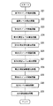
図10は、キャリブレーション回路30による測定誤差およびレベル誤差の算出処理の流れの一例を示す。まず、スイッチ制御部71は、第1から第4のスイッチ41〜44に対して、それぞれ対応する機器を第2の端子412、422、432、442に接続させる(S21:第3のスイッチ制御段階)。次に、基準レベル測定部83は、第2の波形発生器12に所定の信号を出力させ、レベル測定器54が測定した所定の信号のレベルを検出する(S22:基準レベル検出段階)。次に、スイッチ制御部71は、第1から第4のスイッチ41〜44に対して、それぞれ対応する機器を第1の端子411、421、431、441に接続させる(S23:第4のスイッチ制御段階)。次に、レベル測定誤差算出部84は、第2の波形発生器12に所定の信号を出力させ、第2の波形測定器22が測定した所定の信号のレベルを検出する(S24:第1の測定レベル検出段階)。次に、レベル測定誤差算出部84は、基準レベル測定段階において検出した所定の信号のレベルと、第1の測定レベル検出段階において検出した所定の信号のレベルとに基づいて、第2の波形測定器22の測定誤差を算出する(S25:第1の測定誤差算出段階)。
FIG. 10 shows an example of the flow of processing for calculating measurement errors and level errors by the
次に、スイッチ制御部71は、第1から第4のスイッチ41〜44に対して、それぞれ対応する機器を第2の端子412、422、432、442に接続させる(S26:第5のスイッチ制御段階)。次に、レベル測定誤差算出部84は、第1の波形発生器11に所定の信号を出力させ、第1の波形測定器21および第2の波形測定器22が測定した所定の信号のレベルを検出する(S27:第2の測定レベル検出段階)。次に、レベル測定誤差算出部84は、第2の測定レベル検出段階において検出した第1の波形測定器21及び第2の波形測定器22における測定結果の差分、および、第1の測定誤差算出段階において算出した第2の波形測定器22の測定誤差に基づいて、第1の波形測定器21の測定誤差を算出する(S28:第2の測定誤差算出段階)。
Next, the
次に、スイッチ制御部71は、第1から第4のスイッチ41〜44に対して、それぞれ対応する機器を第1の端子411、421、431、441に接続させる(S29:第6のスイッチ制御段階)。次に、出力レベル算出部85は、第1の波形発生器11及び第2の波形発生器12に所定の信号を出力させ、第1の波形測定器21及び第2の波形測定器22が測定した所定の信号のレベルを検出する(S30:出力レベル検出段階)。次に、出力レベル算出部85は、出力レベル検出段階において検出した第1の波形測定器21及び第2の波形測定器22における測定結果の差分、第1の波形発生器11の測定誤差、及び第2の波形発生器12の測定誤差に基づいて、第1の波形測定器21及び第2の波形測定器22が出力する信号のレベル誤差を算出する(S31:出力誤差算出段階)。
Next, the
キャリブレーション回路30によれば、以上のように第1から第4のスイッチ41〜44を切り換えて、それぞれ対応する機器を第2の端子及び第1の端子に交互に接続することによって、第1の波形発生器11及び第2の波形発生器12のレベル誤差並びに第1の波形測定器21及び第2の波形測定器22の測定誤差の両者を測定することができる。これにより、キャリブレーション回路30によれば、簡易な制御により、第1の波形発生器11及び第2の波形発生器12のレベル誤差並びに第1の波形測定器21及び第2の波形測定器22の測定誤差の両者を測定することができる。
According to the
以上、本発明を実施の形態を用いて説明したが、本発明の技術的範囲は上記実施の形態に記載の範囲には限定されない。上記実施の形態に、多様な変更または改良を加えることが可能であることが当業者に明らかである。その様な変更または改良を加えた形態も本発明の技術的範囲に含まれ得ることが、特許請求の範囲の記載から明らかである。 As mentioned above, although this invention was demonstrated using embodiment, the technical scope of this invention is not limited to the range as described in the said embodiment. It will be apparent to those skilled in the art that various modifications or improvements can be added to the above-described embodiment. It is apparent from the scope of the claims that the embodiments added with such changes or improvements can be included in the technical scope of the present invention.
10 試験装置本体部
11 第1の波形発生器
12 第2の波形発生器
21 第1の波形測定器
22 第2の波形測定器
30 キャリブレーション回路
41 第1のスイッチ
42 第2のスイッチ
43 第3のスイッチ
44 第4のスイッチ
51 第1の接続経路
52 第2の接続経路
53 分配経路
54 レベル測定器
55 測定経路
61 第1の抵抗
62 第2の抵抗
63 第3の抵抗
71 スイッチ制御部
81 測定器スキュー算出部
82 発生器スキュー算出部
83 基準レベル測定部
84 レベル測定誤差算出部
85 出力レベル算出部
100 試験装置
411 第1の端子
421 第1の端子
431 第1の端子
441 第1の端子
412 第2の端子
422 第2の端子
432 第2の端子
442 第2の端子
DESCRIPTION OF
Claims (14)
前記第1及び第2の波形発生器、並びに前記第1及び第2の波形測定器に対応して設けられ、前記第1及び第2の波形発生器の出力端、並びに前記第1及び第2の波形測定器の入力端のそれぞれを、第1の端子又は第2の端子のいずれに接続するかを切り替える第1から第4のスイッチと、
前記第1のスイッチの前記第2の端子を、前記第3のスイッチ及び前記第4のスイッチの双方の前記第2の端子に接続する分配経路と、
前記第1のスイッチの前記第1の端子と、前記第3のスイッチの前記第1の端子とを接続する第1の接続経路と、
前記第2のスイッチの前記第1の端子と、前記第4のスイッチの第1の端子とを接続する第2の接続経路と
を備えるキャリブレーション回路。 A calibration circuit for calibrating an apparatus including first and second waveform generators and first and second waveform measuring devices provided corresponding to the first and second waveform generators. And
The first and second waveform generators and the first and second waveform measuring devices are provided corresponding to the output terminals of the first and second waveform generators, and the first and second waveform generators. First to fourth switches for switching each of the input terminals of the waveform measuring device to either the first terminal or the second terminal;
A distribution path connecting the second terminal of the first switch to the second terminal of both the third switch and the fourth switch;
A first connection path connecting the first terminal of the first switch and the first terminal of the third switch;
A calibration circuit comprising: a second connection path that connects the first terminal of the second switch and the first terminal of the fourth switch.
請求項1に記載のキャリブレーション回路。 The calibration circuit according to claim 1, wherein propagation delay times in the distribution path, the first connection path, and the second connection path are substantially equal.
前記第1のスイッチの前記第2の端子に接続される第1の抵抗と、
前記第1の抵抗と、前記第3のスイッチの前記第2の端子との間に接続され、前記第1の抵抗と略同一の抵抗値を有する第2の抵抗と、
前記第1の抵抗と、前記第4のスイッチの前記第2の端子との間に接続され、前記第1の抵抗と略同一の抵抗値を有する第3の抵抗と
を有する請求項1に記載のキャリブレーション回路。 The distribution route is
A first resistor connected to the second terminal of the first switch;
A second resistor connected between the first resistor and the second terminal of the third switch and having substantially the same resistance value as the first resistor;
2. The device according to claim 1, further comprising a third resistor connected between the first resistor and the second terminal of the fourth switch and having substantially the same resistance value as the first resistor. Calibration circuit.
前記第2のスイッチの前記第2の端子と、前記レベル測定器とを接続する測定経路と
を更に備える請求項1に記載のキャリブレーション回路。 A level meter that measures the level of a given signal;
The calibration circuit according to claim 1, further comprising a measurement path that connects the second terminal of the second switch and the level measuring device.
請求項4に記載のキャリブレーション回路。 The first waveform measurement is performed by causing the first waveform generator to output a predetermined signal in a state where corresponding devices are connected to the second terminal with respect to the first to fourth switches. Measuring device skew calculation for calculating a skew between the first waveform measuring device and the second waveform measuring device based on respective timings at which the measuring device and the second waveform measuring device receive the predetermined signal The calibration circuit according to claim 4, further comprising a unit.
請求項5に記載のキャリブレーション回路。 A predetermined signal is output to the first waveform generator and the second waveform generator in a state where corresponding devices are connected to the first terminal with respect to the first to fourth switches, respectively. The first waveform measuring device and the second waveform measuring device detect the timing at which the predetermined signal is received from the corresponding waveform generator, and the timing and the measuring device skew calculation unit calculate the timing. The calibration circuit according to claim 5, further comprising a generator skew calculating unit that calculates a skew between the first waveform generator and the second waveform generator based on a skew.
前記第1から第4のスイッチに対して、それぞれ対応する機器を前記第1の端子に接続させた状態で、前記第2の波形発生器に所定の信号を出力させ、前記第2の波形測定器が測定する前記所定の信号のレベルと、前記基準レベル測定部が測定した前記所定の信号のレベルとに基づいて、前記第2の波形測定器の測定誤差を算出するレベル測定誤差算出部と
を更に備える請求項6に記載のキャリブレーション回路。 With the corresponding devices connected to the second terminal for the first to fourth switches, the second waveform generator outputs a predetermined signal, and the level measuring device A reference level measurement unit for measuring the level of a predetermined signal;
The second waveform measurement is performed by causing the second waveform generator to output a predetermined signal in a state where corresponding devices are connected to the first terminal with respect to the first to fourth switches. A level measurement error calculating unit that calculates a measurement error of the second waveform measuring device based on the level of the predetermined signal measured by the measuring device and the level of the predetermined signal measured by the reference level measuring unit; The calibration circuit according to claim 6, further comprising:
請求項7に記載のキャリブレーション回路。 The level measurement error calculation unit further outputs a predetermined signal to the first waveform generator in a state where corresponding devices are connected to the second terminal for the first to fourth switches. The calibration circuit according to claim 7, wherein the calibration circuit calculates the measurement error of the first waveform measuring device based on a difference between measurement results of the first waveform measuring device and the second waveform measuring device.
請求項8に記載のキャリブレーション回路。 The first waveform generator and the second waveform generator are set to substantially the same level with corresponding devices connected to the first terminal for the first to fourth switches. And detecting the difference between the level measurement results in the first waveform measuring device and the second waveform measuring device, the difference between the level measurement results, the measurement error of the first waveform generator, and The output level calculation part which calculates the level error of the signal which the said 1st waveform measuring device and the said 2nd waveform measuring device output based on the measurement error of the said 2nd waveform generator is further provided in Claim 8. The calibration circuit described.
前記測定器スキュー算出部及び前記基準レベル測定部は、前記第1から第4のスイッチが、それぞれ対応する機器を前記第2の端子に接続した場合に、前記第1の波形測定器と前記第2の波形測定器との間のスキューと、前記レベル測定器における前記所定の信号のレベルの測定結果とを並行して検出する
請求項9に記載のキャリブレーション回路。 A switch control unit that alternately connects corresponding devices to the second terminal and the first terminal with respect to the first to fourth switches,
The measuring instrument skew calculating section and the reference level measuring section are configured such that when the first to fourth switches connect corresponding devices to the second terminal, the first waveform measuring instrument and the first reference level measuring section, respectively. The calibration circuit according to claim 9, wherein a skew between the two waveform measuring devices and a measurement result of the level of the predetermined signal in the level measuring device are detected in parallel.
請求項10に記載のキャリブレーション回路。 The generator skew calculation unit and the level measurement error calculation unit, when the first to fourth switches respectively connect corresponding devices to the first terminal, the first waveform generator and the level measurement error calculation unit The calibration circuit according to claim 10, wherein a skew between the second waveform generator and a measurement error of the second waveform measuring device are detected in parallel.
請求項10に記載のキャリブレーション回路。 The generator skew calculation unit and the output level calculation unit are configured such that when the first to fourth switches connect corresponding devices to the first terminal, the first waveform generator and the first output level calculation unit, respectively. 11. The calibration circuit according to claim 10, wherein a skew between two waveform generators and a level error of signals output from the first waveform measuring device and the second waveform measuring device are detected in parallel.
前記第1から第4のスイッチに対して、それぞれ対応する機器を前記第2の端子に接続させる第1のスイッチ制御段階と、
前記第1の波形発生器に所定の信号を出力させ、前記第1の波形測定器及び前記第2の波形測定器が前記所定の信号を受け取るそれぞれのタイミングを検出する測定タイミング検出段階と、
前記測定タイミング検出段階において検出した前記タイミングに基づいて、前記第1の波形測定器と前記第2の波形測定器との間のスキューを算出する測定器スキュー算出段階と、
前記第1から第4のスイッチに対して、それぞれ対応する機器を前記第1の端子に接続させる第2のスイッチ制御段階と、
前記第1の波形発生器及び前記第2の波形発生器に所定の信号を出力させ、前記第1の波形測定器及び前記第2の波形測定器が、それぞれ対応する前記波形発生器から前記所定の信号を受け取るタイミングを検出する出力タイミング検出段階と、
前記出力タイミング検出段階において検出したタイミング及び前記測定器スキュー算出段階において算出したスキューに基づいて、前記第1の波形発生器と前記第2の波形発生器との間のスキューを算出する発生器スキュー算出段階と
を備えるキャリブレーション方法。 An apparatus comprising first and second waveform generators, a first waveform measuring device corresponding to the first waveform generator, and a second waveform measuring device corresponding to the second waveform generator. A calibration method for performing calibration using the calibration circuit according to claim 1,
A first switch control stage for connecting corresponding devices to the second terminal for the first to fourth switches,
A measurement timing detecting step of outputting a predetermined signal to the first waveform generator and detecting respective timings at which the first waveform measuring instrument and the second waveform measuring instrument receive the predetermined signal;
A measuring device skew calculating step for calculating a skew between the first waveform measuring device and the second waveform measuring device based on the timing detected in the measuring timing detecting step;
A second switch control stage for connecting corresponding devices to the first terminal for the first to fourth switches;
The first waveform generator and the second waveform generator are caused to output predetermined signals, and the first waveform measuring device and the second waveform measuring device are respectively transmitted from the corresponding waveform generator to the predetermined waveform generator. Output timing detection stage for detecting the timing of receiving the signal of,
Generator skew for calculating a skew between the first waveform generator and the second waveform generator based on the timing detected in the output timing detection stage and the skew calculated in the measuring instrument skew calculation stage A calibration method comprising a calculation stage.
前記被試験デバイスに対して並列に供給する第1及び第2の試験信号を生成する第1及び第2の波形発生器と、
前記被試験デバイスが並列に出力する第1及び第2の出力信号を測定する第1及び第2の波形測定器と、
前記第1及び第2の波形発生器、並びに前記第1及び第2の波形測定器をキャリブレーションするキャリブレーション回路と
を備え、
前記キャリブレーション回路は、
前記第1及び第2の波形発生器、並びに前記第1及び第2の波形測定器に対応して設けられ、前記第1及び第2の波形発生器の出力端、並びに前記第1及び第2の波形測定器の入力端のそれぞれを、第1の端子又は第2の端子のいずれに接続するかを切り替える第1から第4のスイッチと、
前記第1のスイッチの前記第2の端子を、前記第3のスイッチ及び前記第4のスイッチの双方の前記第2の端子に接続する分配経路と、
前記第1のスイッチの前記第1の端子と、前記第3のスイッチの前記第1の端子とを接続する第1の接続経路と、
前記第2のスイッチの前記第1の端子と、前記第4のスイッチの第1の端子とを接続する第2の接続経路と
を有する試験装置。
A test apparatus for testing a device under test,
First and second waveform generators for generating first and second test signals to be supplied in parallel to the device under test;
First and second waveform measuring devices for measuring first and second output signals output in parallel by the device under test;
A calibration circuit for calibrating the first and second waveform generators and the first and second waveform measuring devices;
The calibration circuit includes:
The first and second waveform generators and the first and second waveform measuring devices are provided corresponding to the output terminals of the first and second waveform generators, and the first and second waveform generators. First to fourth switches for switching each of the input terminals of the waveform measuring device to either the first terminal or the second terminal;
A distribution path connecting the second terminal of the first switch to the second terminal of both the third switch and the fourth switch;
A first connection path connecting the first terminal of the first switch and the first terminal of the third switch;
A test apparatus comprising: a second connection path that connects the first terminal of the second switch and the first terminal of the fourth switch.
Priority Applications (1)
| Application Number | Priority Date | Filing Date | Title |
|---|---|---|---|
| JP2006111311A JP4714067B2 (en) | 2006-04-13 | 2006-04-13 | Calibration circuit, calibration method, and test apparatus |
Applications Claiming Priority (1)
| Application Number | Priority Date | Filing Date | Title |
|---|---|---|---|
| JP2006111311A JP4714067B2 (en) | 2006-04-13 | 2006-04-13 | Calibration circuit, calibration method, and test apparatus |
Publications (2)
| Publication Number | Publication Date |
|---|---|
| JP2007285779A true JP2007285779A (en) | 2007-11-01 |
| JP4714067B2 JP4714067B2 (en) | 2011-06-29 |
Family
ID=38757702
Family Applications (1)
| Application Number | Title | Priority Date | Filing Date |
|---|---|---|---|
| JP2006111311A Expired - Fee Related JP4714067B2 (en) | 2006-04-13 | 2006-04-13 | Calibration circuit, calibration method, and test apparatus |
Country Status (1)
| Country | Link |
|---|---|
| JP (1) | JP4714067B2 (en) |
Cited By (1)
| Publication number | Priority date | Publication date | Assignee | Title |
|---|---|---|---|---|
| CN113126014A (en) * | 2021-04-14 | 2021-07-16 | 中国工程物理研究院计量测试中心 | Calibration system for realizing array parallelism of digital oscilloscope |
Citations (7)
| Publication number | Priority date | Publication date | Assignee | Title |
|---|---|---|---|---|
| JPH04196908A (en) * | 1990-11-28 | 1992-07-16 | Mitsubishi Electric Corp | Distortion compensating circuit for amplifier |
| JP2000341123A (en) * | 1999-03-24 | 2000-12-08 | Advantest Corp | A/d converter and calibration device |
| JP2001021620A (en) * | 1999-07-07 | 2001-01-26 | Mitsubishi Electric Corp | Lsi testing apparatus and its timing calibrating method |
| JP2001141777A (en) * | 1999-11-16 | 2001-05-25 | Sharp Corp | Test device for integrated circuit |
| WO2002101404A1 (en) * | 2001-06-07 | 2002-12-19 | Advantest Corporation | Method for calibrating semiconductor test instrument |
| JP2003057314A (en) * | 2001-06-06 | 2003-02-26 | Agilent Technol Inc | Device and method for testing digital device using transition time stamp |
| JP2003133954A (en) * | 2001-10-26 | 2003-05-09 | Agilent Technologies Japan Ltd | Calibration method for interleave system a/d converter |
-
2006
- 2006-04-13 JP JP2006111311A patent/JP4714067B2/en not_active Expired - Fee Related
Patent Citations (7)
| Publication number | Priority date | Publication date | Assignee | Title |
|---|---|---|---|---|
| JPH04196908A (en) * | 1990-11-28 | 1992-07-16 | Mitsubishi Electric Corp | Distortion compensating circuit for amplifier |
| JP2000341123A (en) * | 1999-03-24 | 2000-12-08 | Advantest Corp | A/d converter and calibration device |
| JP2001021620A (en) * | 1999-07-07 | 2001-01-26 | Mitsubishi Electric Corp | Lsi testing apparatus and its timing calibrating method |
| JP2001141777A (en) * | 1999-11-16 | 2001-05-25 | Sharp Corp | Test device for integrated circuit |
| JP2003057314A (en) * | 2001-06-06 | 2003-02-26 | Agilent Technol Inc | Device and method for testing digital device using transition time stamp |
| WO2002101404A1 (en) * | 2001-06-07 | 2002-12-19 | Advantest Corporation | Method for calibrating semiconductor test instrument |
| JP2003133954A (en) * | 2001-10-26 | 2003-05-09 | Agilent Technologies Japan Ltd | Calibration method for interleave system a/d converter |
Cited By (2)
| Publication number | Priority date | Publication date | Assignee | Title |
|---|---|---|---|---|
| CN113126014A (en) * | 2021-04-14 | 2021-07-16 | 中国工程物理研究院计量测试中心 | Calibration system for realizing array parallelism of digital oscilloscope |
| CN113126014B (en) * | 2021-04-14 | 2024-04-02 | 中国工程物理研究院计量测试中心 | Calibration system for realizing array parallelism of digital oscilloscope |
Also Published As
| Publication number | Publication date |
|---|---|
| JP4714067B2 (en) | 2011-06-29 |
Similar Documents
| Publication | Publication Date | Title |
|---|---|---|
| JP5279724B2 (en) | Test apparatus and calibration method | |
| JP5161878B2 (en) | Noise measuring device and test device | |
| JP2006300688A (en) | Calibration method and calibration system | |
| KR100868995B1 (en) | Test Apparatus, Regulating Apparatus, Regulating Method, and Computer Readable Medium on which Regulating Program is recorded | |
| KR20120139795A (en) | Measurement device and measurement method | |
| JP2011172208A (en) | Output apparatus and test apparatus | |
| JP4948421B2 (en) | Test apparatus, adjustment apparatus, adjustment method, and adjustment program | |
| JP2008107188A (en) | Testing device, driver comparator chip, response measuring device, and calibration method and device | |
| KR101178069B1 (en) | Interconnect circuit board, skew measuring method and testing device | |
| JP4714067B2 (en) | Calibration circuit, calibration method, and test apparatus | |
| JP5066184B2 (en) | Test equipment and transmission equipment | |
| JP2009103469A (en) | Testing device, skew measuring device, device, and board | |
| JP2007212279A (en) | Timing calibration method and its device | |
| JPWO2002068976A1 (en) | Propagation delay time measurement method and test equipment | |
| JP2007292471A (en) | Semiconductor tester | |
| JP2009156580A (en) | Input capacitance measuring circuit | |
| JP5024146B2 (en) | Semiconductor test equipment with timing calibration function | |
| JP2007040849A (en) | Measuring equipment and test equipment | |
| TWI596348B (en) | Measuring device | |
| US20150168189A1 (en) | Method for determination of the time of flight of the signals in the signal paths of a coriolis flow meter | |
| JP2010054314A (en) | Semiconductor tester | |
| WO2010087009A1 (en) | Electronic device, test equipment, and test method | |
| JP2011095079A (en) | Semiconductor testing apparatus | |
| JP4900031B2 (en) | Semiconductor test equipment | |
| JP5249357B2 (en) | Electronic device, test apparatus and test method |
Legal Events
| Date | Code | Title | Description |
|---|---|---|---|
| A621 | Written request for application examination |
Free format text: JAPANESE INTERMEDIATE CODE: A621 Effective date: 20090126 |
|
| A977 | Report on retrieval |
Free format text: JAPANESE INTERMEDIATE CODE: A971007 Effective date: 20100826 |
|
| A131 | Notification of reasons for refusal |
Free format text: JAPANESE INTERMEDIATE CODE: A131 Effective date: 20100907 |
|
| A521 | Request for written amendment filed |
Free format text: JAPANESE INTERMEDIATE CODE: A523 Effective date: 20101025 |
|
| A01 | Written decision to grant a patent or to grant a registration (utility model) |
Free format text: JAPANESE INTERMEDIATE CODE: A01 Effective date: 20110322 |
|
| A61 | First payment of annual fees (during grant procedure) |
Free format text: JAPANESE INTERMEDIATE CODE: A61 Effective date: 20110325 |
|
| FPAY | Renewal fee payment (event date is renewal date of database) |
Free format text: PAYMENT UNTIL: 20140401 Year of fee payment: 3 |
|
| LAPS | Cancellation because of no payment of annual fees |