JP2007266533A - Plasma treatment apparatus and plasma treatment method - Google Patents
Plasma treatment apparatus and plasma treatment method Download PDFInfo
- Publication number
- JP2007266533A JP2007266533A JP2006092908A JP2006092908A JP2007266533A JP 2007266533 A JP2007266533 A JP 2007266533A JP 2006092908 A JP2006092908 A JP 2006092908A JP 2006092908 A JP2006092908 A JP 2006092908A JP 2007266533 A JP2007266533 A JP 2007266533A
- Authority
- JP
- Japan
- Prior art keywords
- frequency
- electrode
- plasma
- processing
- impedance
- Prior art date
- Legal status (The legal status is an assumption and is not a legal conclusion. Google has not performed a legal analysis and makes no representation as to the accuracy of the status listed.)
- Granted
Links
Images


Classifications
-
- H—ELECTRICITY
- H01—ELECTRIC ELEMENTS
- H01J—ELECTRIC DISCHARGE TUBES OR DISCHARGE LAMPS
- H01J37/00—Discharge tubes with provision for introducing objects or material to be exposed to the discharge, e.g. for the purpose of examination or processing thereof
- H01J37/32—Gas-filled discharge tubes
- H01J37/32009—Arrangements for generation of plasma specially adapted for examination or treatment of objects, e.g. plasma sources
- H01J37/32082—Radio frequency generated discharge
- H01J37/32174—Circuits specially adapted for controlling the RF discharge
-
- H—ELECTRICITY
- H01—ELECTRIC ELEMENTS
- H01J—ELECTRIC DISCHARGE TUBES OR DISCHARGE LAMPS
- H01J37/00—Discharge tubes with provision for introducing objects or material to be exposed to the discharge, e.g. for the purpose of examination or processing thereof
- H01J37/32—Gas-filled discharge tubes
- H01J37/32009—Arrangements for generation of plasma specially adapted for examination or treatment of objects, e.g. plasma sources
- H01J37/32082—Radio frequency generated discharge
- H01J37/32091—Radio frequency generated discharge the radio frequency energy being capacitively coupled to the plasma
-
- H—ELECTRICITY
- H01—ELECTRIC ELEMENTS
- H01J—ELECTRIC DISCHARGE TUBES OR DISCHARGE LAMPS
- H01J37/00—Discharge tubes with provision for introducing objects or material to be exposed to the discharge, e.g. for the purpose of examination or processing thereof
- H01J37/32—Gas-filled discharge tubes
- H01J37/32009—Arrangements for generation of plasma specially adapted for examination or treatment of objects, e.g. plasma sources
- H01J37/32082—Radio frequency generated discharge
- H01J37/32137—Radio frequency generated discharge controlling of the discharge by modulation of energy
- H01J37/32155—Frequency modulation
- H01J37/32165—Plural frequencies
Abstract
Description
本発明は、被処理基板にプラズマ処理を施す技術に係り、特に2周波重畳印加方式の容量結合型プラズマ処理装置およびプラズマ処理方法に関する。 The present invention relates to a technique for performing plasma processing on a substrate to be processed, and more particularly to a capacitively coupled plasma processing apparatus and a plasma processing method of a two-frequency superimposition application method.
半導体デバイスやFPD(Flat Panel Display)の製造プロセスにおけるエッチング、堆積、酸化、スパッタリング等の処理では、処理ガスに比較的低温で良好な反応を行わせるためにプラズマがよく利用されている。従来より、枚葉式のプラズマ処理装置、特にプラズマエッチング装置の中では、容量結合型のプラズマ処理装置が主流となっている。 In processes such as etching, deposition, oxidation, sputtering and the like in the manufacturing process of semiconductor devices and FPDs (Flat Panel Displays), plasma is often used in order to cause a favorable reaction to a processing gas at a relatively low temperature. Conventionally, among single-wafer plasma processing apparatuses, particularly plasma etching apparatuses, capacitively coupled plasma processing apparatuses have been mainstream.
一般に、容量結合型プラズマ処理装置は、真空チャンバとして構成される処理容器内に上部電極と下部電極とを平行に配置し、下部電極の上に被処理基板(半導体ウエハ、ガラス基板等)を載置し、両電極のいずれか一方に高周波電圧を印加する。この高周波電圧によって両電極間に形成される電界により電子が加速され、電子と処理ガスとの衝突電離によってプラズマが発生し、プラズマ中のラジカルやイオンによって基板表面に所望の微細加工(たとえばエッチング加工)が施される。ここで、高周波を印加される側の電極は整合器内のブロッキングキャパシタを介して高周波電源に接続されるため、カソード(陰極)として働く。基板を支持する下部電極に高周波を印加してこれをカソードとするカソードカップル方式は、下部電極に生じる自己バイアス電圧を利用してプラズマ中のイオンを基板にほぼ垂直に引き込むことにより、異方性エッチングを可能としている。 Generally, in a capacitively coupled plasma processing apparatus, an upper electrode and a lower electrode are arranged in parallel in a processing container configured as a vacuum chamber, and a substrate to be processed (semiconductor wafer, glass substrate, etc.) is mounted on the lower electrode. And a high frequency voltage is applied to one of both electrodes. Electrons are accelerated by the electric field formed between both electrodes by this high-frequency voltage, and plasma is generated by impact ionization between the electrons and the processing gas, and desired microfabrication (for example, etching processing) is performed on the substrate surface by radicals or ions in the plasma. ) Is given. Here, the electrode to which the high frequency is applied is connected to a high frequency power source via a blocking capacitor in the matching unit, and thus functions as a cathode (cathode). The cathode-coupled method, in which a high frequency is applied to the lower electrode that supports the substrate and this is used as the cathode, is anisotropic by drawing ions in the plasma almost perpendicularly to the substrate using the self-bias voltage generated in the lower electrode. Etching is possible.
下部2周波重畳印加方式は、上記のような容量結合型プラズマ処理装置において、基板を支持する下部電極にプラズマ生成に適した比較的高い周波数(一般に27MHz以上)の第1高周波とイオン引き込みに適した比較的低い周波数(一般に13.56MHz以下)の第2高周波とを重畳して印加するものである(たとえば特許文献1参照)。 In the capacitively coupled plasma processing apparatus as described above, the lower two-frequency superimposed application method is suitable for the first high frequency and ion attraction of a relatively high frequency (generally 27 MHz or more) suitable for plasma generation in the lower electrode supporting the substrate. In addition, the second high frequency having a relatively low frequency (generally 13.56 MHz or less) is applied in a superimposed manner (see, for example, Patent Document 1).
このような下部2周波重畳印加方式は、プラズマの密度および異方性エッチングの選択性を第1高周波および第2高周波によりそれぞれ個別的に最適化できるという利点があることに加えて、上部電極にポリマー等の堆積物(デポジション、以下“デポ”と略称する。)が付着しやすいプロセスにおいてデポ付着の防止ないし抑制に比較的低い周波数の第2高周波が有効に作用するという利点も有している。すなわち、アノードの上部電極にイオンが入射すると、電極に付いているデポ膜が(酸化膜が付いていればそれも)イオン衝撃でスパッタされる。このスパッタリングに関係するイオンの数は第1高周波が作り、そのイオンを加速する電界は第2高周波の比較的低い周波数によって作られる。
上記のような下部2周波重畳印加方式を用いる従来の容量結合型プラズマ処理装置は、概して、高周波を印加しないアノード側の上部電極を直流的に接地している。通常は、処理容器がアルミニウムやステンレス等の金属からなり保安接地されるので、処理容器を通じて上部電極を接地電位にすることができることから、上部電極を処理容器の天井に直付けで一体に組み込む構成や、あるいは処理容器の天井をそのまま上部電極として利用する構成を採っている。 The conventional capacitively coupled plasma processing apparatus using the lower two-frequency superimposed application method as described above generally grounds the upper electrode on the anode side to which no high frequency is applied in a DC manner. Normally, the processing vessel is made of a metal such as aluminum or stainless steel and is grounded for safety, so that the upper electrode can be grounded through the processing vessel, so the upper electrode is directly attached to the ceiling of the processing vessel and integrated integrally. Alternatively, a configuration is employed in which the ceiling of the processing vessel is used as it is as the upper electrode.
しかしながら、近年の半導体製造プロセスにおけるデザインルールの微細化につれて低圧下での高密度のプラズマが要求されている。下部2周波重畳印加方式の容量結合型プラズマ処理装置ではプラズマ生成に主として寄与する高周波つまり第1高周波の周波数が段々高くなってきており、最近は標準的に40MHz以上の周波数を使用している。ところが、第1高周波の周波数が高くなると、その高周波電流が電極の中心部に集まることによって、両電極間の処理空間に生成されるプラズマの密度も電極中心部側が電極エッジ部側より高くなり、プロセスの面内均一性が低下するという問題がクローズアップされてきている。一方、イオン引き込み用に主として寄与する高周波つまり第2高周波の周波数は比較的低いため、電極中心部に集中することはない。つまり、上部電極を処理容器に直付けまたは一体に形成して直流的に接地する従来の装置においては、第2高周波の作用、つまり基板へのイオン引き込みや上部電極におけるデポ付着の抑制に関する作用について特に問題点は見られない。 However, with the recent miniaturization of design rules in semiconductor manufacturing processes, high-density plasma under low pressure is required. In the capacitively coupled plasma processing apparatus of the lower two-frequency superimposing application method, the frequency of the high frequency, which mainly contributes to plasma generation, that is, the frequency of the first high frequency is gradually increased, and recently, a frequency of 40 MHz or higher is typically used. However, when the frequency of the first high frequency is increased, the high-frequency current is collected at the center of the electrode, so that the density of plasma generated in the processing space between both electrodes is higher on the electrode center side than on the electrode edge side, The problem of reduced in-plane uniformity of the process has been highlighted. On the other hand, the high frequency mainly contributing to the ion attraction, that is, the frequency of the second high frequency is relatively low, so that it does not concentrate at the electrode center. In other words, in the conventional apparatus in which the upper electrode is directly attached to or integrally formed with the processing vessel and grounded in a direct current manner, the second high-frequency action, that is, the action related to the ion attraction into the substrate and the suppression of the deposit on the upper electrode There is no particular problem.
本発明は、上記のような従来技術の問題点に鑑みてなされたものであって、被処理基板を支持する電極に2種類の高周波を重畳して印加する2周波重畳印加方式の容量結合型において、他方の対向電極に不所望な膜が形成されるのを十全に防止ないし抑制しつつプラズマ密度の空間的な分布特性を任意に制御してプロセスの面内均一性を向上させるプラズマ処理装置およびプラズマ処理方法を提供することを目的とする。 The present invention has been made in view of the above-described problems of the prior art, and is a capacitively coupled type of a two-frequency superimposition application method in which two types of high frequencies are superimposed and applied to an electrode that supports a substrate to be processed. Plasma processing to improve the in-plane uniformity of the process by arbitrarily controlling the spatial distribution characteristics of the plasma density while completely preventing or suppressing the formation of an undesired film on the other counter electrode An object is to provide an apparatus and a plasma processing method.
上記の目的を達成するために、本発明の第1のプラズマ処理装置は、真空排気可能な接地された処理容器と、前記処理容器に絶縁物または空間を介して取り付けられる第1の電極と、前記処理容器内に前記第1の電極と所定の間隔を空けて平行に配置され、前記第1の電極と対向させて被処理基板を支持する第2の電極と、前記第2の電極に第1の周波数を有する第1の高周波を印加する第1の高周波給電部と、前記第2の電極に前記第1の周波数よりも低い第2の周波数を有する第2の高周波を印加する第2の高周波給電部と、前記第1の電極と前記第2の電極と前記処理容器の側壁との間の処理空間に所望の処理ガスを供給する処理ガス供給部と、前記第1の電極と接地電位との間に電気的に接続されるインダクタとを有する。 In order to achieve the above object, a first plasma processing apparatus of the present invention includes a grounded processing container capable of being evacuated, a first electrode attached to the processing container via an insulator or a space, A second electrode that is disposed in parallel with the first electrode in the processing container at a predetermined interval and that supports the substrate to be processed so as to face the first electrode, and a second electrode on the second electrode. A first high-frequency power feeding unit that applies a first high frequency having a frequency of 1; and a second high-frequency power supply that applies a second high frequency having a second frequency lower than the first frequency to the second electrode. A high-frequency power supply unit, a processing gas supply unit that supplies a desired processing gas to a processing space between the first electrode, the second electrode, and a sidewall of the processing container; the first electrode; and a ground potential And an inductor electrically connected to each other.
また、本発明の第1のプラズマ処理方法は、真空可能な接地された処理容器内で第1の電極と第2の電極とを所定の間隔を空けて平行に配置し、前記第1の電極を電気的に並列な容量性の部材と誘導性の部材とを介して接地電位に接続し、前記第1の電極に対向させて被処理基板を第2の電極で支持し、前記処理容器内を所定の圧力に真空排気し、前記第2の電極に第1の周波数を有する第1の高周波と前記第1の周波数よりも低い第2の周波数を有する第2の高周波とを印加しながら、前記第1の電極と前記第2の電極と前記処理容器の側壁との間の処理空間に所望の処理ガスを供給して前記処理空間内で前記処理ガスのプラズマを生成し、前記プラズマの下で前記基板に所望の処理を施すプラズマ処理方法であって、前記処理空間と前記第1の電極との境界面から前記第1の電極を介して接地電位に至るまでの高周波伝送路を見込んだときの周波数−インピーダンス特性において、前記第1の周波数に対応するインピーダンスよりも前記第2の周波数に対応するインピーダンスが低くなるように、前記周波数−インピーダンス特性を設定する。 Further, in the first plasma processing method of the present invention, the first electrode and the second electrode are arranged in parallel at a predetermined interval in a vacuum-grounded processing container, and the first electrode Is connected to a ground potential through an electrically parallel capacitive member and an inductive member, and the substrate to be processed is supported by the second electrode so as to face the first electrode. Is evacuated to a predetermined pressure, and a first high frequency having a first frequency and a second high frequency having a second frequency lower than the first frequency are applied to the second electrode, A desired processing gas is supplied to a processing space between the first electrode, the second electrode, and a side wall of the processing container to generate a plasma of the processing gas in the processing space. A plasma processing method for performing a desired process on the substrate in the processing space and the process In the frequency-impedance characteristic when a high-frequency transmission path from the boundary surface with one electrode to the ground potential through the first electrode is expected, the second impedance is higher than the impedance corresponding to the first frequency. The frequency-impedance characteristic is set so that the impedance corresponding to the frequency of the frequency becomes low.
本発明の採る容量結合型においては、第1の高周波電源からの第1の高周波が第2の電極に印加されると、第2の電極と第1の電極との間の高周波放電および第2の電極と処理容器の側壁(内壁)との間の高周波放電によって処理空間内で処理ガスのプラズマが生成し、生成したプラズマは四方に、特に上方および半径方向外側に拡散し、プラズマ中の電子電流は第1の電極や処理容器側壁等を通ってグランドへ流れる。また、第2の高周波電源からの第2の高周波が第2の電極に印加されると、第2の高周波に追従して振動するプラズマ中のイオンが第2の電極に生じる自己バイアスで基板上に引き込まれるだけでなく第1の電極にも入射してその電極表面をスパッタし、デポジション等の膜が付着していればそれを除去する。 In the capacitively coupled type according to the present invention, when the first high frequency from the first high frequency power supply is applied to the second electrode, the high frequency discharge between the second electrode and the first electrode and the second The plasma of the processing gas is generated in the processing space by the high-frequency discharge between the electrode and the side wall (inner wall) of the processing vessel, and the generated plasma diffuses in all directions, particularly upward and radially outward, and the electrons in the plasma The current flows to the ground through the first electrode, the processing container side wall, and the like. Further, when a second high frequency from the second high frequency power source is applied to the second electrode, ions in the plasma that vibrate following the second high frequency are generated on the substrate by self-bias generated in the second electrode. In addition to being drawn into the first electrode, it also enters the first electrode and sputters the surface of the electrode, and if a film such as deposition adheres, it is removed.
本発明によれば、第1の電極が、絶縁物または空間を介して接地電位の処理容器内に取り付けられる一方で、誘導性の部材またはインダクタを介して接地電位に接続される。これにより、処理空間と第1の電極との境界面から第1の電極を介して接地電位までの高周波伝送路を見込んだときの等価回路は、インダクタのコイル分と絶縁物等の容量分とを並列に接続した並列LC回路となる。 According to the present invention, the first electrode is mounted in a processing container having a ground potential through an insulator or a space, while being connected to the ground potential through an inductive member or an inductor. Thus, an equivalent circuit when a high-frequency transmission path from the boundary surface between the processing space and the first electrode to the ground potential through the first electrode is expected includes the inductor coil and the capacity of the insulator, etc. Are parallel LC circuits connected in parallel.
一般に、並列LC回路においては、或る特定の周波数(反共振周波数)でインピーダンスが突出して高くなる反面、反共振周波数から離れた周波数ではインピーダンスが相当低くなる。この特性を利用することで、本発明のプラズマ処理装置においては、第1の高周波に対しては高めのインピーダンスを与え、第2の高周波に対しては低めのインピーダンスを与えることができる。本発明の好適な一態様によれば、上記等価回路または並列LC回路の周波数−インピーダンス特性において5〜200MHzの帯域内に反共振周波数が得られる。 In general, in a parallel LC circuit, the impedance protrudes and increases at a specific frequency (anti-resonance frequency), but the impedance decreases considerably at frequencies away from the anti-resonance frequency. By utilizing this characteristic, in the plasma processing apparatus of the present invention, a higher impedance can be given to the first high frequency and a lower impedance can be given to the second high frequency. According to a preferred aspect of the present invention, an anti-resonance frequency is obtained within a band of 5 to 200 MHz in the frequency-impedance characteristics of the equivalent circuit or the parallel LC circuit.
第1の高周波に対して高めのインピーダンスを与えることで、第1の高周波の電流が第2の電極から第1の電極へ流れ難くなる。このため、プラズマの電子電流の中で処理容器の側壁へ流れる割合が相対的に増大し、プラズマの密度は半径方向外側へ拡がるようになる。こうして、上記並列LC回路の第1の高周波に対するインピーダンスを高めの値に最適化することで、プラズマの密度の空間分布特性を径方向で均一化することも任意に制御することも可能となる。一方で、上記並列LC回路の第2の高周波に対するインピーダンスを低くすることで、第2高周波に追従して振動するプラズマ中のイオンを第1の電極に強い衝撃で入射せしめて、その電極表面に付着する不所望な膜を良好にスパッタ(除去)することができる。 By giving a higher impedance to the first high frequency, it becomes difficult for the first high frequency current to flow from the second electrode to the first electrode. For this reason, the ratio of the plasma electron current flowing to the side wall of the processing vessel relatively increases, and the density of the plasma spreads outward in the radial direction. Thus, by optimizing the impedance of the parallel LC circuit with respect to the first high frequency to a higher value, the spatial distribution characteristics of the plasma density can be made uniform in the radial direction or arbitrarily controlled. On the other hand, by reducing the impedance of the parallel LC circuit with respect to the second high frequency, ions in the plasma that vibrates following the second high frequency are caused to enter the first electrode with a strong impact, and are applied to the surface of the electrode. It is possible to satisfactorily sputter (remove) the undesired film that adheres.
本発明の第2のプラズマ処理装置は、真空排気可能な接地された処理容器と、前記処理容器に絶縁物または空間を介して取り付けられる第1の電極と、前記処理容器内に前記第1の電極と所定の間隔を空けて平行に配置され、前記第1の電極と対向させて被処理基板を支持する第2の電極と、前記第2の電極に第1の周波数を有する第1の高周波を印加する第1の高周波給電部と、前記第2の電極に前記第1の周波数よりも低い第2の周波数を有する第2の高周波を印加する第2の高周波給電部と、前記第1の電極と前記第2の電極と前記処理容器の側壁との間の処理空間に所望の処理ガスを供給する処理ガス供給部と、前記第1の電極と接地電位との間で電気的に直列に接続されるインダクタおよびコンデンサとを有する。 The second plasma processing apparatus of the present invention includes a grounded processing container capable of being evacuated, a first electrode attached to the processing container via an insulator or a space, and the first electrode in the processing container. A second electrode that is arranged in parallel with the electrode at a predetermined interval and that supports the substrate to be processed so as to face the first electrode; and a first high frequency signal having a first frequency in the second electrode A first high-frequency power supply unit that applies a second high-frequency power supply unit that applies a second high frequency having a second frequency lower than the first frequency to the second electrode, and the first A processing gas supply unit that supplies a desired processing gas to a processing space between the electrode, the second electrode, and the sidewall of the processing vessel; and electrically in series between the first electrode and a ground potential An inductor and a capacitor to be connected;
本発明の第2のプラズマ処理方法は、真空可能な接地された処理容器内で第1の電極と第2の電極とを所定の間隔を空けて平行に配置し、前記第1の電極を電気的に直並列の誘導性の部材と容量性の部材とを介して接地電位に接続し、前記第1の電極に対向させて被処理基板を第2の電極で支持し、前記処理容器内を所定の圧力に真空排気し、前記第2の電極に第1の周波数を有する第1の高周波と前記第1の周波数よりも低い第2の周波数を有する第2の高周波とを印加しながら、前記第1の電極と前記第2の電極と前記処理容器の側壁との間の処理空間に所望の処理ガスを供給して前記処理空間内に前記処理ガスのプラズマを生成し、前記プラズマの下で前記基板に所望のプラズマ処理を施すプラズマ処理方法であって、前記処理空間と前記第1の電極との境界面から前記第1の電極を介して接地電位に至るまでの高周波伝送路を見込んだときの周波数−インピーダンス特性において、前記第1の周波数に対応するインピーダンスよりも前記第2の周波数に対応するインピーダンスが低くなるように、前記周波数−インピーダンス特性を設定する。 In the second plasma processing method of the present invention, the first electrode and the second electrode are arranged in parallel at a predetermined interval in a vacuum-grounded processing container, and the first electrode is electrically connected. In particular, the substrate is connected to the ground potential via a series-parallel inductive member and a capacitive member, the substrate to be processed is supported by the second electrode so as to face the first electrode, and the inside of the processing container is While evacuating to a predetermined pressure and applying a first high frequency having a first frequency and a second high frequency having a second frequency lower than the first frequency to the second electrode, A desired processing gas is supplied to a processing space between the first electrode, the second electrode, and the side wall of the processing container to generate plasma of the processing gas in the processing space. A plasma processing method for performing desired plasma processing on the substrate, wherein the processing space and In the frequency-impedance characteristic when a high-frequency transmission path from the boundary surface with the first electrode to the ground potential through the first electrode is expected, the impedance is higher than the impedance corresponding to the first frequency. The frequency-impedance characteristic is set so that the impedance corresponding to the second frequency is low.
上記第2のプラズマ処理装置および方法においては、処理空間と第1の電極との境界面から第1の電極を介して接地電位までの高周波伝送路を見込んだときの等価回路が直並列LC回路として構成される。この直並列LC回路においては、或る特定の周波数(共振周波数)でインピーダンスが極端に低くなり、別の特定の周波数(反共振周波数)でインピーダンスが極端に高くなる。この特性を利用し、第1の高周波に対して適当な高めのインピーダンスを与えることができるのはもちろん、第2の高周波に対して著しく低いインピーダンスを与えることができる。本発明の好適な一態様によれば、上記等価回路または直並列LC回路の周波数−インピーダンス特性において、0.1kHz〜15MHzの帯域内に共振周波数が得られ、5〜200MHzの帯域内に反共振周波数が得られる。こうして、上記直並列LC回路の第1の高周波に対するインピーダンスを高めの値に最適化することで、プラズマの密度の空間分布特性を径方向で均一化したり任意に制御することができるとともに、上記並列LC回路の第2の高周波に対するインピーダンスを実質的に短絡状態まで低くすることで、第1の電極の表面から不所望な膜を除去するスパッタ効果を一層高めることができる。 In the second plasma processing apparatus and method, an equivalent circuit when a high-frequency transmission path from the boundary surface between the processing space and the first electrode to the ground potential through the first electrode is expected is a series-parallel LC circuit. Configured as In this series-parallel LC circuit, the impedance is extremely low at a certain specific frequency (resonance frequency), and the impedance is extremely high at another specific frequency (anti-resonance frequency). Using this characteristic, it is possible not only to give an appropriately high impedance to the first high frequency, but also to give a remarkably low impedance to the second high frequency. According to a preferred aspect of the present invention, in the frequency-impedance characteristics of the above-described equivalent circuit or series-parallel LC circuit, a resonance frequency is obtained in the band of 0.1 kHz to 15 MHz and anti-resonance is in the band of 5 to 200 MHz. The frequency is obtained. Thus, by optimizing the impedance of the series-parallel LC circuit with respect to the first high frequency to a high value, the spatial distribution characteristics of the plasma density can be made uniform in the radial direction or arbitrarily controlled, and the parallel By reducing the impedance of the LC circuit to the second high frequency to a substantially short-circuited state, it is possible to further enhance the sputtering effect for removing an undesired film from the surface of the first electrode.
本発明の第3のプラズマ処理装置は、真空排気可能な接地された処理容器と、前記処理容器に絶縁物または空間を介して取り付けられる第1の電極と、前記処理容器内に前記第1の電極と所定の間隔を空けて平行に配置され、前記第1の電極と対向させて被処理基板を支持する第2の電極と、前記第2の電極に第1の周波数を有する第1の高周波を印加する第1の高周波給電部と、前記第2の電極に前記第1の周波数よりも低い第2の周波数を有する第2の高周波を印加する第2の高周波給電部と、前記第1の電極と前記第2の電極と前記処理容器の側壁との間の処理空間に所望の処理ガスを供給する処理ガス供給部と、前記第1の電極に所望の直流電圧を印加する直流電源と、前記第1の電極と前記直流電源との間に電気的に接続され、直流を実質的にスルーで通し、高周波に対しては所望の周波数−インピーダンス特性を有するフィルタとを有する。 The third plasma processing apparatus of the present invention includes a grounded processing container capable of being evacuated, a first electrode attached to the processing container via an insulator or a space, and the first electrode in the processing container. A second electrode that is arranged in parallel with the electrode at a predetermined interval and that supports the substrate to be processed so as to face the first electrode; and a first high frequency signal having a first frequency in the second electrode A first high-frequency power supply unit that applies a second high-frequency power supply unit that applies a second high frequency having a second frequency lower than the first frequency to the second electrode, and the first A processing gas supply unit that supplies a desired processing gas to a processing space between an electrode, the second electrode, and a sidewall of the processing container; a DC power source that applies a desired DC voltage to the first electrode; An electrical connection is made between the first electrode and the DC power source, Substantially passes in through the relative high-frequency desired frequency - and a filter having an impedance characteristic.
上記第3のプラズマ処理装置は、フィルタを介して直流電源から第1の電極に所望の直流電圧を印加してその分の作用効果を奏するとともに、フィルタ自体の周波数−インピーダンス特性によって第1および第2高周波の各作用に所望の補正ないし制御あるいはアシストを及ぼすことができる。たとえば、該フィルタを直並列LC回路に構成することで、上記の第2のプラズマ処理装置と同様に、プラズマ密度の空間分布特性や第1の電極に対するスパッタ(不所望な膜の除去)効果を向上させることができる。 In the third plasma processing apparatus, a desired DC voltage is applied to the first electrode from a DC power source via the filter, and the operation effect is obtained. Further, the first and second plasma processing apparatuses have a frequency-impedance characteristic of the filter itself. Desired correction, control, or assist can be applied to each of the two high-frequency actions. For example, by constructing the filter in a series-parallel LC circuit, the spatial distribution characteristics of the plasma density and the sputtering effect on the first electrode (removal of undesired films) can be achieved as in the case of the second plasma processing apparatus. Can be improved.
本発明のプラズマ処理装置およびプラズマ処理方法によれば、上記のような構成および作用により、2周波重畳印加方式の容量結合型において第1および第2の高周波の各作用のトレードオフを解決することができる。特に、他方の対向電極に不所望な膜が形成されるのを十全に防止ないし抑制しつつ、プラズマ密度の空間的な分布特性を任意に制御してプロセスの面内均一性を向上させることができる。 According to the plasma processing apparatus and the plasma processing method of the present invention, the trade-off between the first and second high-frequency actions can be solved in the capacitive coupling type of the two-frequency superimposing application method by the configuration and action as described above. Can do. In particular, the in-plane uniformity of the process can be improved by arbitrarily controlling the spatial distribution characteristics of the plasma density while thoroughly preventing or suppressing the formation of an undesired film on the other counter electrode. Can do.
以下、添付図を参照して本発明の好適な実施の形態を説明する。 Hereinafter, preferred embodiments of the present invention will be described with reference to the accompanying drawings.
図1に、本発明の第1の実施形態におけるプラズマ処理装置の構成を示す。このプラズマ処理装置は、下部2周波重畳印加方式の容量結合型(平行平板型)プラズマエッチング装置として構成されており、たとえば表面がアルマイト処理(陽極酸化処理)されたアルミニウムからなる円筒形の真空チャンバ(処理容器)10を有している。チャンバ10は保安接地されている。
FIG. 1 shows a configuration of a plasma processing apparatus according to the first embodiment of the present invention. This plasma processing apparatus is configured as a capacitive coupling type (parallel plate type) plasma etching apparatus of a lower two-frequency superimposing application system, and for example, a cylindrical vacuum chamber made of aluminum whose surface is anodized (anodized). (Processing container) 10 is provided. The
チャンバ10の底部には、セラミックなどの絶縁板12を介して円柱状のサセプタ支持台14が配置され、このサセプタ支持台14の上にたとえばアルミニウムからなるサセプタ16が設けられている。サセプタ16は下部電極を構成し、この上に被処理基板としてたとえば半導体ウエハWが載置される。
A
サセプタ16の上面には半導体ウエハWを静電吸着力で保持するための静電チャック18が設けられている。この静電チャック18は導電膜からなる電極20を一対の絶縁層または絶縁シートの間に挟み込んだものであり、電極20には直流電源22が電気的に接続されている。直流電源22からの直流電圧により、半導体ウエハWをクーロン力で静電チャック18に吸着保持できるようになっている。静電チャック18の周囲でサセプタ16の上面には、エッチングの均一性を向上させるためのたとえばシリコンからなるフォーカスリング24が配置されている。サセプタ16およびサセプタ支持台14の側面にはたとえば石英からなる円筒状の内壁部材25が貼り付けられている。
An
サセプタ支持台14の内部には、たとえば円周方向に延びる冷媒室26が設けられている。この冷媒室26には、外付けのチラーユニット(図示せず)より配管27a,27bを介して所定温度の冷媒たとえば冷却水が循環供給される。冷媒の温度によってサセプタ16上の半導体ウエハWの処理温度を制御できるようになっている。さらに、伝熱ガス供給機構(図示せず)からの伝熱ガスたとえばHeガスが、ガス供給ライン28を介して静電チャック18の上面と半導体ウエハWの裏面との間に供給される。
Inside the
サセプタ16には、第1および第2の高周波電源30,70がそれぞれ整合器32,72および給電棒33,74を介して電気的に接続されている。第1の高周波電源30は、プラズマの生成に主として寄与する所定の周波数たとえば40MHzの高周波を出力する。一方、第2の高周波電源70は、サセプタ16上の半導体ウエハWに対するイオンの引き込みと後述する上部電極34におけるデポや酸化膜等の不所望な膜の付着の防止ないし除去に主として寄与する所定の周波数たとえば2MHzの高周波を出力する。
The
サセプタ16の上方には、このサセプタと平行に対向して上部電極34が設けられている。この上部電極34は、多数のガス噴出孔36aを有するたとえばSi、SiCなどの半導体材料からなる電極板36と、この電極板36を着脱可能に支持する導電材料たとえば表面がアルマイト処理されたアルミニウムからなる電極支持体38とで構成されており、チャンバ10にリング状の絶縁体35を介して電気的に浮いた状態で取り付けられている。この上部電極34とサセプタ16とチャンバ10の側壁とでプラズマ生成空間または処理空間PSが形成されている。リング状絶縁体35は、たとえばアルミナ(Al2O3)からなり、上部電極34の外周面とチャンバ10の側壁との間の隙間を気密に塞ぐように取り付けられ、上部電極34を物理的に支持するとともに、電気的には上部電極34とチャンバ10との間の容量の一部を構成している。
An
電極支持体38は、その内部にガスバッファ室40を有するとともに、その下面にガスバッファ室40から電極板36のガス噴出孔36aに連通する多数のガス通気孔38aを有している。ガスバッファ室40にはガス供給管42を介して処理ガス供給源44が接続されており、ガス供給管42にマスフローコントローラ(MFC)46および開閉バルブ48が設けられている。処理ガス供給源44より所定の処理ガスがガスバッファ室40に導入されると、電極板36のガス噴出孔36aよりサセプタ16上の半導体ウエハWに向けて処理空間PSに処理ガスがシャワー状に噴出されるようになっている。このように、上部電極34は処理空間PSに処理ガスを供給するためのシャワーヘッドを兼ねている。
The
また、電極支持体38の内部には冷媒たとえば冷却水を流す通路(図示せず)も設けられており、外部のチラーユニットにより冷媒を介して上部電極34の全体、特に電極板36を所定温度に温調するようになっている。さらに、上部電極34に対する温度制御をより安定化させるために、電極支持体38の内部または上面にたとえば抵抗発熱素子からなるヒータ(図示せず)を取り付ける構成も可能である。
Further, a passage (not shown) through which a coolant such as cooling water flows is provided inside the
上部電極34の上面とチャンバ10の天井との間には中空の空間または隙間50が設けられるとともに、チャンバ10の上面の中心部に貫通孔52が形成され、隙間50と貫通孔52の中で鉛直方向に延びる棒状のインダクタ54が設けられている。この棒状インダクタ54は、下端が上部電極34の上面中心部に直に接続され、上端が導線56を介して接地電位に(通常はチャンバ10に)接続されている。別の実施例として、棒状インダクタ54の上端が上部電極34の天井に直付けで接続される構成も可能である。
A hollow space or
サセプタ16およびサセプタ支持台14とチャンバ10の側壁との間に形成される環状の空間は排気空間となっており、この排気空間の底にはチャンバ10の排気口58が設けられている。この排気口58に排気管60を介して排気装置62が接続されている。排気装置62は、ターボ分子ポンプなどの真空ポンプを有しており、チャンバ10の室内、特に処理空間PSを所望の真空度まで減圧できるようになっている。また、チャンバ10の側壁には半導体ウエハWの搬入出口64を開閉するゲートバルブ66が取り付けられている。
An annular space formed between the susceptor 16 and the
このプラズマエッチング装置において、エッチングを行なうには、先ずゲートバルブ66を開状態にして加工対象の半導体ウエハWをチャンバ10内に搬入して、静電チャック18の上に載置する。そして、処理ガス供給源44より所定の処理ガスつまりエッチングガス(一般に混合ガス)を所定の流量および流量比でチャンバ10内に導入し、排気装置62による真空排気でチャンバ10内の圧力を設定値にする。さらに、第1および第2の高周波電源30,70よりそれぞれ所定のパワーで第1高周波(40MHz)および第2高周波(2MHz)を重畳してサセプタ16に印加する。また、直流電源22より直流電圧を静電チャック18の電極20に印加して、半導体ウエハWを静電チャック18上に固定する。上部電極34のシャワーヘッドより吐出されたエッチングガスは処理空間PSで高周波の放電によってプラズマ化し、このプラズマで生成されるラジカルやイオンによって半導体ウエハWの主面の膜がエッチングされる。
In order to perform etching in this plasma etching apparatus, first, the
この容量結合型プラズマエッチング装置は、サセプタ(下部電極)16に40MHzというプラズマ生成に適した比較的高い周波数の第1高周波を印加することにより、プラズマを好ましい解離状態で高密度化し、より低圧の条件下でも高密度プラズマを形成することができると同時に、サセプタ16に2MHzというイオン引き込みに適した比較的低い周波数の第2高周波を印加することにより、静電チャック18上の半導体ウエハWに対して選択性の高い異方性のエッチングを施すとともに、上部電極34に対してはイオンの入射またはスパッタリングによるデポ膜や酸化膜の除去(電極表面の清浄化)を施すことができる。
In this capacitively coupled plasma etching apparatus, by applying a first high frequency of a relatively high frequency suitable for plasma generation of 40 MHz to a susceptor (lower electrode) 16, the plasma is densified in a preferable dissociation state, and a lower pressure is obtained. A high-density plasma can be formed even under conditions, and at the same time, by applying a second high frequency of a relatively low frequency suitable for ion attraction of 2 MHz to the
次に、図2〜図4につき、この実施形態のプラズマエッチング装置における本発明の特徴的な作用について説明する。なお、図2および図3は、図解の便宜上、プラズマの生成ないし空間分布制御に実質的に関係しない第2の高周波電源70を省いている。
Next, the characteristic operation of the present invention in the plasma etching apparatus of this embodiment will be described with reference to FIGS. 2 and 3 omit the second high-
上述したように、このプラズマエッチング装置は、上部電極34をチャンバ10にリング状絶縁体35を介して取り付けるとともに、上部電極34と接地電位との間に棒状インダクタ54を接続している。すなわち、インダクタ54を外せば上部電極34は直流的にフローティング状態で処理容器10内に設置される構成になっている。
As described above, in this plasma etching apparatus, the
先ず、比較例として、上部電極34をたとえばチャンバ10に直付けで取り付けて直流的に接地電位に接続した場合の作用を説明する。この場合は、図2に示すように、高周波電源30からの第1高周波がサセプタ16に印加されると、サセプタ16と上部電極34との間の高周波放電およびサセプタ16とチャンバ10の側壁との間の高周波放電によって処理空間PS内で処理ガスのプラズマが生成し、生成したプラズマは四方に、特に上方および半径方向外側に拡散し、プラズマ中の電子電流は上部電極34やチャンバ10の側壁等を通ってグランドへ流れる。ここで、サセプタ16においては第1高周波の周波数が高くなるほど表皮効果によってサセプタ中心部に高周波電流が集まりやすく、しかもサセプタ16からみて同電位(グランド電位)にある上部電極34とチャンバ10側壁とでは前者の方が後者よりも距離的に近いため、電極中心部でより多くの高周波電力が処理空間PSに向けて放出される。このため、プラズマの電子電流の中でチャンバ10の側壁へ流れる割合はかなり低く、大部分は上部電極34に、しかもその中心部に流れる。その結果、プラズマ密度の空間分布特性は、電極中心部が最も高いだけでなく、電極エッジ部との差が顕著に現れる。
First, as a comparative example, the operation when the
これに対して、この実施形態のように上部電極34を直流的にフローティング状態でチャンバ10に取り付け、かつ棒状インダクタ54を介して接地電位に接続する構成においては、処理空間PSと上部電極34との境界面から上部電極34を介して接地電位までの高周波伝送路を見込んだときの等価回路が、図3に示すようにコイルL54とキャパシタC35,C50とを並列に接続したものになる。ここで、コイルL54は棒状インダクタ54のインダクタンス分であり、正確にはこのコイルL54に棒状インダクタ54の抵抗分(図示せず)が直列に接続される。一方のキャパシタC35は上部電極34とチャンバ10の側壁との間の容量であり、主としてリング状絶縁体35によって与えられる。他方のキャパシタC50は上部電極34とチャンバ10の天井との間の容量であり、主として隙間50内の空気によって与えられる。
On the other hand, in the configuration in which the
この場合も、高周波電源30より第1高周波がサセプタ16に印加されると、サセプタ16と上部電極34との間の高周波放電およびサセプタ16とチャンバ10の側壁との間の高周波放電によって処理空間PS内でエッチングガスのプラズマが生成し、生成したプラズマは上方および半径方向外側に拡散し、プラズマ中の電子電流は上部電極34やチャンバ10の側壁等を通ってグランドへ流れる。そして、サセプタ16においてはサセプタ中心部に高周波電流が集まりやすく、サセプタ16からみてチャンバ10の側壁よりも上部電極34の方が近くに位置しているのも図2の場合と同じである。しかし、上部電極34と接地電位との間にコイルL54とキャパシタC35,C50とからなる並列LC回路80が存在しており、第1高周波に対してこの並列LC回路80が大きなインピーダンスZを与えるときは、サセプタ16の中心部に高周波電流が集まってもそこから真上の上部電極34へは流れにくくなる。このため、プラズマの電子電流の中でチャンバ10の側壁へ流れる割合が相対的に増大し、プラズマの密度は半径方向外側へ拡がるようになる。理論的には並列LC回路80のインピーダンスZ次第で如何様にもサセプタ16と上部電極34との間およびサセプタ16とチャンバ10の側壁との間でそれぞれ流れる電子電流の比を制御し、ひいてはプラズマ密度の空間分布特性を径方向で均一化することも任意に制御することもできる。
Also in this case, when the first high frequency is applied from the high
図4に、このプラズマエッチング装置において処理空間PSと上部電極34との境界面から上部電極34を介して接地電位までの高周波伝送路を見込んだときの周波数−インピーダンス特性の一例を示す。図中、周波数に対して単調に増加するインピーダンスXLはコイルL54の誘導性リアクタンス(|jωL54|)であり、周波数に対して単調に減少するインピーダンスXCはキャパシタC35,C50の容量性リアクタンス(|1/jω(C35+C50)|)である。理論的には、それら誘導性リアクタンスXLと容量性リアクタンスXCとが同じ大きさ(絶対値)になる周波数で並列LC回路80が並列共振または反共振を起こし、図示のように並列LC回路80のインピーダンスZはその反共振周波数foで角状に突出した極大値を示す。この反共振周波数foは第1高周波の周波数を含む帯域(好ましくは5〜200MHz)内に現れるのが好ましい。
FIG. 4 shows an example of frequency-impedance characteristics when a high-frequency transmission path from the boundary surface between the processing space PS and the
したがって、図示のように第1高周波の周波数(40MHz)の近傍に(極端には一致して)反共振周波数foが得られるように任意に可変または選択可能なパラメータつまりインダクタ54のインダクタンスを選定または設定することで、第1高周波に対する並列LC回路80のインピーダンスZを任意の高めの値Z40に選ぶことができる。
Therefore, as shown in the drawing, a parameter that can be arbitrarily changed or selected, that is, the inductance of the
さらに重要なことは、図4に示すように、反共振周波数foを上記のような帯域(5〜200MHz)内に設定することで、第2高周波に対する並列LC回路80のインピーダンスZ80を第1高周波に対する値Z40よりも桁違いに低い値Z2に選定できるという点である。つまり、第2高周波に対して上部電極34を低いインピーダンスで接地できるという点である。これにより、第2高周波に追従して振動するプラズマ中のイオンを上部電極34の電極板36に強い衝撃で入射せしめて、電極板36の表面に付着するデポ膜や酸化膜を確実にスパッタ(除去)することができる。
More importantly, as shown in FIG. 4, by setting the anti-resonance frequency f o within the above band (5 to 200 MHz), the impedance Z 80 of the
図5Aおよび図5Bに、この実施形態のプラズマエッチング装置による酸化膜(SiO2)およびフォトレジスト(PR)のエッチングレートの面内分布特性の一実施例を示す。この実施例では、インダクタ54のインダクタンスを400nH、キャパシタC35,C50の合成容量を250pF(低容量)に選んでいる。また、図6〜図7に比較例を示す。すなわち、図6Aおよび図6Bに、第1の比較例として、インダクタ54を省いてキャパシタC35,C50の合成容量を20000pF(高容量)に選んだ場合の酸化膜およびフォトレジストのエッチングレートの空間分布特性をそれぞれ示す。また、図7Aおよび図7Bに、第2の比較例として、インダクタ54を省いてキャパシタC35,C50の合成容量を250pF(低容量)に選んだ場合の酸化膜およびフォトレジストのエッチングレートの空間分布特性をそれぞれ示す。実施例および比較例において共通する主なエッチング条件は下記のとおりである。
ウエハ口径:300mm
処理ガス:C4F6/C4F8/Ar/02=流量40/20/500/60sccm
チャンバ内の圧力:30mTorr
高周波電力:40MHz/2MHz=2500/3200W
温度:上部電極の温度=60℃
5A and 5B show an example of in-plane distribution characteristics of the etching rate of the oxide film (S i O 2 ) and the photoresist (PR) by the plasma etching apparatus of this embodiment. In this embodiment, the inductance of the
Wafer diameter: 300 mm
Process gas: C 4 F 6 / C 4 F 8 / Ar / 0 2 =
Pressure in chamber: 30mTorr
High frequency power: 40MHz / 2MHz = 2500 / 3200W
Temperature: Upper electrode temperature = 60 ° C.
図6Aおよび図6Bからわかるように、インダクタ54を備えずに上部電極34の接地容量を高容量(20000pF)に設定した第1の比較例においては、酸化膜のエッチングレートおよびフォトレジストのエッチングレートのいずれもウエハ中心部では比較的フラットな値を保つが、ウエハエッジ付近で(R=±120mm辺りから)急峻に低下するため、それらの面内均一性はそれぞれ±4.1%,±19.1%とあまりよくない。
6A and 6B, in the first comparative example in which the ground capacitance of the
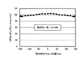
一方、インダクタ54を備えずに上部電極34の接地容量を低容量(250pF)に設定した第2の比較例においては、図6Aおよび図6Bに示すように、プロセスの均一性が第1の比較例に比して大幅に向上する。より詳細には、酸化膜のエッチングレートは、第1の比較例と較べてウエハ中心部では大して違わないがエッジ部で上昇し、それによって面内均一性は±2.4%に向上している。また、フォトレジストのエッチングレートは、ウエハ上の各位置で増大してかなりフラットな分布になり、面内均一性は±4.4%まで大幅に改善している。
On the other hand, in the second comparative example in which the ground capacitance of the
これに対して、実施例においては、図5Aおよび図5Bから明らかなように、プロセスの均一性が第2の比較例よりも一層向上している。より詳細には、酸化膜のエッチングレートは、ウエハ上の各位置で上昇し、とりわけエッジ部で大幅に上昇し、面内均一性は±1.2%まで向上している。また、フォトレジストのエッチングレートも、ウエハ上の各位置で殆ど均一であり、面内均一性は±2.5%まで改善している。 On the other hand, in the example, as is apparent from FIGS. 5A and 5B, the uniformity of the process is further improved as compared with the second comparative example. More specifically, the etching rate of the oxide film increases at each position on the wafer, particularly at the edge portion, and the in-plane uniformity is improved to ± 1.2%. Also, the etching rate of the photoresist is almost uniform at each position on the wafer, and the in-plane uniformity is improved to ± 2.5%.
一般に、酸化膜のエッチングレート分布はプラズマ中の電子密度分布つまりプラズマ密度分布を反映し、フォトレジストのエッチングレート分布はプラズマによる母ガスの解離の影響を受けるため一層強くプラズマ密度分布に依存する。したがって、図5Aおよび図5Bの実験結果から、実施例によれば、処理空間PSで生成するプラズマを電極中心部に集中するのを抑制して半径方向外側へ拡げ、プラズマ密度分布の均一性を大きく向上させていることがわかる。 In general, the etching rate distribution of the oxide film reflects the electron density distribution in plasma, that is, the plasma density distribution, and the etching rate distribution of the photoresist is more strongly dependent on the plasma density distribution because it is affected by the dissociation of the mother gas by the plasma. Therefore, from the experimental results of FIGS. 5A and 5B, according to the embodiment, the plasma generated in the processing space PS is restrained from concentrating on the center of the electrode and spread outward in the radial direction, and the uniformity of the plasma density distribution is improved. It can be seen that it is greatly improved.
上記のように、第2の比較例においても、第1の比較例に比してプラズマ密度分布の均一性を相当改善できることがわかる。しかしながら、インダクタ54を備えない第2の比較例は、上部電極34の接地回路を構成する低容量(250pF)のキャパシタC35,C50が第1高周波(40MHz)に対してだけでなく第2高周波(2MHz)に対しても相当高いインピーダンスを与える。より正確には、図4の容量性リアクタンスXCの周波数特性から理解されるように、第1高周波(40MHz)に対するよりも第2高周波(2MHz)に対するインピーダンスの方が高くなる。このように第2高周波に対して上部電極34の接地回路のインピーダンスが高いと、第2高周波に追従して上部電極34に入射するイオンの衝撃は弱まり、スパッタ効果が低減するという不都合が出てくる。
As described above, it is understood that the uniformity of the plasma density distribution can be considerably improved in the second comparative example as compared with the first comparative example. However, the second comparative example having no
この点、実施例は、インダクタ54を備えることで、並列LC回路80のインピーダンスを第1高周波(40MHz)に対しては任意の高めの値に選定できると同時に第2高周波(2MHz)に対しては相当低い値に選定できる。このことによって、上述のようにプラズマ密度分布の均一性を大幅に改善する一方で、上部電極34に入射するイオンの衝撃強度ひいてはスパッタリング(電極表面の清浄化)の効果を十二分に保つことができる。
In this regard, in the embodiment, by providing the
一例として、エッチングガスにポリマーの発生量が多いC4F8を使用し、実施例と第2の比較例とで上部電極34の表面にデポ膜が付着するレート(デポレート)を測定したところ、第2の比較例では80nm/5分、実施例では−100nm/5分の測定結果が得られた。このデポレート定量化実験における主なエッチング条件は下記のとおりである。
処理ガス:C4F8/Ar=流量5/1000sccm
チャンバ内の圧力:40mTorr
高周波電力:40MHz/2MHz=2000/400W
温度:上部電極/チャンバ側壁/下部電極=150/150/40℃
エッチング時間:5分
As an example, when C 4 F 8 with a large amount of polymer generated is used as an etching gas, the rate at which the deposition film adheres to the surface of the upper electrode 34 (deposition) in the example and the second comparative example was measured. In the second comparative example, the measurement result was 80 nm / 5 minutes, and in the example, the measurement result was −100 nm / 5 minutes. The main etching conditions in this deposition rate quantification experiment are as follows.
Process gas: C 4 F 8 / Ar = flow rate 5/1000 sccm
Pressure in chamber: 40 mTorr
High frequency power: 40MHz / 2MHz = 2000 / 400W
Temperature: Upper electrode / chamber sidewall / lower electrode = 150/150/40 ° C.
Etching time: 5 minutes
このように、第2の比較例では上部電極34の表面にデポ膜が累積的に付着するのに対して、実施例では上部電極34の表面からデポ膜をエッチングモードで効率よく除去できることが確認された。
As described above, in the second comparative example, the deposition film is accumulated on the surface of the
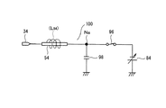
図8に、第2の実施形態におけるプラズマエッチング装置の構成を示す。第1の実施形態がインダクタ54の上端を導線56を介して接地したのに対して、この第2の実施形態はインダクタ54の上端にDCフィルタユニット82を介して可変直流電源84を電気的に接続している点が異なる。他の部分の構成および機能は第1の実施形態と同じである。
FIG. 8 shows the configuration of the plasma etching apparatus in the second embodiment. In contrast to the first embodiment in which the upper end of the
図9に、DCフィルタユニット82内の回路構成例を示す。この実施例のDCフィルタユニット82は、可変直流電源84から上部電極34までの直流伝送路上にインダクタ54と直列に2個のコイル86,88を接続し、両コイル86,88間のノードN1と接地電位との間、およびコイル88と可変直流電源84間のノードN2と接地電位との間にコンデンサ90,92をそれぞれ接続しており、これらのコイル86,88およびコンデンサ90,92で直並列のLC回路94を構成している。
FIG. 9 shows a circuit configuration example in the
なお、DCフィルタユニット82内のそれぞれの電気部品または電気素子を適正な温度に保つため、DCフィルタユニット82の内部にはファン等の冷却(送風)機構が設けられてよい。また、このDCフィルタユニット82は、インダクタ54と可変直流電源84との間であれば任意の位置に配置可能であるが、好ましくはチャンバ10の天井(上面)の上に載置されるのがよい。
In addition, in order to keep each electric component or electric element in the
可変直流電源84より出力される直流電圧は、直並列LC回路94のコイル88,86およびインダクタ54を介して上部電極34に印加される。一方、高周波電源30,70よりサセプタ16に印加される第1,第2高周波は、処理空間PSを介して上部電極34に入ると、そこから先はインダクタ54およびDCフィルタユニット82内の直並列LC回路94を通ってグランドへ流れ、可変直流電源84側へは殆ど流れないようになっている。
The DC voltage output from the variable
可変直流電源84は、プロセスの種類や条件に応じて任意の極性および電圧レベルを有する直流電圧を出力するように構成されている。上部電極34に適度な直流電圧を印加することにより、(1)上部電極34の自己バイアス電圧の絶対値を大きくして上部電極34におけるスパッタリング(デポ除去)を強める効果、(2)上部電極34におけるプラズマシースを拡大させ、形成されるプラズマが縮小化される効果、(3)上部電極34の近傍に生じた電子を被処理基板(半導体ウエハW)上に照射させる効果、(4)プラズマポテンシャルを制御できる効果、(5)電子密度(プラズマ密度)を上昇させる効果、(6)中心部のプラズマ密度を上昇させる効果の少なくとも1つを奏することが知られている。なお、上部電極34に直流電圧を印加する必要のない場合に備えて、可変直流電源84と直並列LC回路94との間にたとえばリレースイッチからなるオン・オフ切替用のスイッチ96を設けるのが好ましい。
The variable
この実施形態においては、DCフィルタユニット82内の直並列LC回路94が可変直流電源84からの直流電圧をスルーで上部電極34側へ通すとともに、上部電極34側からの高周波に対して低域(好ましくは100kHz〜15MHz)で直列共振を起こし、高域(好ましくは5〜200MHz)で並列共振を起こすように構成され、かかる直並列LC回路94の周波数−インピーダンス特性を利用して下部2周波重畳印加方式における第1および第2高周波の各個別の作用を一層向上させるようにしている。
In this embodiment, the series-
図10に、この実施形態において、直並列LC回路94単独の周波数−インピーダンス特性Z94および処理空間PSと上部電極34との境界面から上部電極34を介して接地電位までの高周波伝送路を見込んだときの周波数−インピーダンス特性ZAの一例を示す。
FIG. 10 shows a frequency-impedance characteristic Z 94 of the series-
図10に示すように、この実施例は、直並列LC回路94の共振周波数を約2MHzに設定し、反共振周波数を約45MHzに設定している。この周波数−インピーダンス特性Z94においては、第1高周波(40MHz)に対応するインピーダンスは相当高めの約1000Ωであるのに対して、第2高周波(2MHz)に対応するインピーダンスが約1Ωと極端に低い。この直並列LC回路94にインダクタ54やキャパシタC35,C50等が合わさった上部電極34周囲全体の接地回路の周波数−インピーダンス特性ZAは、反共振周波数が約10MHzまで低域側にシフトするものの、共振周波数は依然として2MHz近辺の値を保っている。そして、第1高周波(40MHz)に対応するインピーダンスは約20Ωまで大きく低下する一方で、第2高周波(2MHz)に対応するインピーダンスは約0.7Ωに若干低くなり、両インピーダンスの間にはまだ20倍以上の開きがある。
As shown in FIG. 10, in this embodiment, the resonance frequency of the series-
図10において特に注目すべきことは、直並列LC回路94の共振現象を利用することにより、上部電極34回り全体の接地回路の周波数−インピーダンス特性ZAにおいても第2高周波(2MHz)に対応するインピーダンスを1Ω以下に低くできる点である。このことによって、第2高周波(2MHz)からみて上部電極34はあたかも接地電位に短絡(イマジナリショート)されている状態となり、第2高周波に倣った振動で上部電極34に入射するイオンの衝撃力ひいてはスパッタリング(デポ除去)効果を可及的に高められる。
What should be particularly noted in FIG. 10 is that the resonance phenomenon of the series-
なお、図10に示す周波数−インピーダンス特性Z94,ZAは一例であり、直並列LC回路94においてコイル86,88のインダクタンスおよびコンデンサ90,92のキャパシタンスの値を変えることで適宜変更または調整することができる。
Note that the frequency-impedance characteristics Z 94 and Z A shown in FIG. 10 are examples, and in the series-
また、図9の回路構成は一例であり、DCフィルタユニット82内やその回りで種々の変形が可能である。たとえば、直並列LC回路94は任意の数のコイルおよびコンデンサで構成可能であり、回路網の形式は図9の¬型に限らず、T型、π型等でもよい。また、直並列LC回路94と可変直流電源84との間に他の機能のための回路素子たとえばノイズ除去用のコイル(図示せず)等を挿入することも可能である。
Further, the circuit configuration of FIG. 9 is an example, and various modifications can be made in and around the
また、DCフィルタユニット82内に可変インピーダンス素子を備えることも可能である。たとえば、図11に示すように、コイル86を可変リアクタ、コンデンサ90を可変コンデンサとすることも可能である。
It is also possible to provide a variable impedance element in the
さらには、直並列LC回路94の代用として、図12に示すように、上部電極34をインダクタ54およびコンデンサ98からなる直列LC回路100を介して接地する構成も可能である。この場合、上部電極34の周囲全体の接地回路としては、つまり処理空間PSと上部電極34との境界面から上部電極34を介して接地電位までの高周波伝送路を見込んだときの等価回路としては、この直列LC回路100にキャパシタC35,C50(図3)を並列に接続してなる直並列LC回路(図示せず)が形成される。この直並列LC回路の周波数−インピーダンス特性において、図10に示したものと同様に、所定の帯域内で所望の共振周波数とこれより高い所望の反共振周波数とが得られるように、好ましくは共振周波数が第2高周波の周波数の極近傍に得られるように、インダクタ54のインダクタンスおよびコンデンサ98のキャパシタンスを設定すればよい。
Furthermore, as a substitute for the series-
また、図12に示すように、可変直流電源84を用いる場合は、可変直流電源84の出力端子をインダクタ54とコンデンサ98との間のノードNaに電気的に接続すればよい。もっとも、可変直流電源84を省く構成も可能である。その場合、上部電極34に対してインダクタ54とコンデンサ98とを入れ換える構成、つまり上部電極34とインダクタ54との間にコンデンサ98を直列に接続する構成も可能である。インダクタ54は、棒状の導体に限定されず、コイル状の導体からなるものでもよく、容量性のインピーダンスを与える任意の誘導性素子または部材を使用できる。
As shown in FIG. 12, when the variable
また、実施形態のプラズマエッチング装置において、上部電極34の周囲の静電容量または接地容量を可変することも可能であり、図13〜図15に静電容量可変部の構成例を示す。
In the plasma etching apparatus of the embodiment, the electrostatic capacity or the ground capacity around the
図13および図14に示す静電容量可変部102は、上部電極34の上面に接触または近接する第1の位置と上部電極34から上方に離れた第2の位置との間で移動可能な導体板104と、この導体板104を上下に移動または変位させるための操作機構106と、操作機構106を通じて上部電極34の接地容量を所望の値に制御するための静電容量制御部108とを有する。図13の操作機構106は、導電性の材質、または高周波に対して導電性の性質を持つ材質、または高周波に対して低インピーダンスの材質からなり、直接あるいはチャンバ10を介して接地される。図14の操作機構106は絶縁性の材質でもよい。この静電容量可変方式は、導体板104の高さ位置に応じて上部電極34の接地容量を可変することが可能である。導体板104をチャンバ10の天井面に近づければ近づけるほど、上部電極34の接地容量を小さくすることができる。反対に、導体板104を上部電極34の上面に近づければ近づけるほど、上部電極34の接地容量を大きくすることができる。極端には上部電極34に導体板104を接触させて上部電極34を接地し、接地容量を無限大にすることもできる。
The
図15に示す静電容量可変部102は、上部電極34とチャンバ10の側壁との間に設けられるリング状絶縁体35の中に環状の液体収容室110を形成し、配管112を介してチャンバ10の外から適当な誘電率を有する液体(たとえばガルデンのような有機溶剤)Qを出し入れできる構成としている。液体Qの種類(誘電率)または液量を変えることでリング状絶縁体35全体の静電容量ひいては上部電極34の接地容量を可変することができる。
The
別の構成例として、上部電極34とチャンバ10との間に可変コンデンサ(図示せず)を接続する構成も可能である。
As another configuration example, a variable capacitor (not shown) may be connected between the
そして、これら可変コンデンサや静電容量可変部102、インダクタ54のインダクタンス可変の可変インダクタンス素子(図示せず)、図11に示すDCフィルタユニット82内の可変インピーダンス素子等を適宜組み合わせることで、任意の周波数−インピーダンス特性を実現することができる。より詳細には、上で述べた可変コンデンサや静電容量可変部102によって、プラズマ生成に主に寄与する第1の高周波に対するインピーダンス値を調整し、DCフィルタユニット82内の可変インピーダンス素子によって、イオン引き込みに主に寄与する第2高周波に対するインピーダンスの値を調整することが可能となる。
An arbitrary combination of these variable capacitors,
また、一実施形態として、図16のような構成を採ることも可能である。具体的には、サセプタ16に高周波電源30より整合器32および給電棒33を介して第1高周波を給電するとともに、高周波電源70より整合器72および給電棒74を介して第2高周波を給電し(下部2周波重畳印加方式)、かつ上部電極を半径方向において円盤状の内側上部電極34とリング状の外側上部電極122とに2分割する構成である。内側上部電極34と外側上部電極122との間にはリング状の絶縁体120が挿入され、外側上部電極122とチャンバ10の側壁との間にはリング状の絶縁体124が挿入される。かかる構成によれば、高い周波数の第1高周波を主として外側上部電極122を通ってチャンバ10の側壁(アース)に至る経路で流れやすくし、低い周波数の第2高周波を主として内側上部電極34および導体棒52を通ってアースに至る経路で流れやすくすることができる。
Further, as an embodiment, a configuration as shown in FIG. 16 can be adopted. Specifically, the first high frequency is supplied from the high
上記した実施形態で使用した第1および第2高周波のそれぞれの周波数は一例であり、プロセスに応じて任意の周波数を使用できる。通常、プラズマの生成に主として寄与する第1高周波の周波数は13.5MHz以上の値に選ばれ、基板へのイオン引き込みや上部電極へのイオン引き込みに主として寄与する第2高周波の周波数は13.56MHz以下の値に選ばれてよい。 Each frequency of the 1st and 2nd high frequency used by the above-mentioned embodiment is an example, and arbitrary frequencies can be used according to a process. Usually, the frequency of the first high frequency that mainly contributes to plasma generation is selected to be 13.5 MHz or more, and the frequency of the second high frequency that mainly contributes to ion attraction to the substrate and ions to the upper electrode is 13.56 MHz. The following values may be chosen.
上記した実施形態による上部電極34回りの接地回路以外に限らず、装置内の各部の構成または機能について種々の変形が可能である。上記実施形態はプラズマエッチング装置およびプラズマエッチング方法に係るものであったが、本発明はプラズマCVD、プラズマ酸化、プラズマ窒化、スパッタリングなどの他の平行平板型プラズマ処理装置および処理方法にも適用可能である。また、本発明における被処理基板は半導体ウエハに限るものではなく、フラットパネルディスプレイ用の各種基板や、フォトマスク、CD基板、プリント基板等も可能である。
In addition to the ground circuit around the
10 チャンバ(処理容器)
16 サセプタ(下部電極)
30 第1の高周波電源
34 上部電極
35 リング状絶縁体
36 電極板
36a ガス噴出孔
38 電極支持体
40 ガスバッファ室
42 ガス供給管
44 処理ガス供給源
50 隙間
54 インダクタ
70 第2の高周波電源
82 DCフィルタユニット
84 可変直流電源
86,88 コイル
90,92,98 コンデンサ
94,100 直並列LC回路
10 chamber (processing vessel)
16 Susceptor (lower electrode)
30 First High
Claims (29)
前記処理容器に絶縁物または空間を介して取り付けられる第1の電極と、
前記処理容器内に前記第1の電極と所定の間隔を空けて平行に配置され、前記第1の電極と対向させて被処理基板を支持する第2の電極と、
前記第2の電極に第1の周波数を有する第1の高周波を印加する第1の高周波給電部と、
前記第2の電極に前記第1の周波数よりも低い第2の周波数を有する第2の高周波を印加する第2の高周波給電部と、
前記第1の電極と前記第2の電極と前記処理容器の側壁との間の処理空間に所望の処理ガスを供給する処理ガス供給部と、
前記第1の電極と接地電位との間に電気的に接続されるインダクタと
を有するプラズマ処理装置。 A grounded processing vessel capable of being evacuated;
A first electrode attached to the processing vessel via an insulator or space;
A second electrode disposed in parallel with the first electrode in the processing container at a predetermined interval and supporting the substrate to be processed so as to face the first electrode;
A first high-frequency power feeding unit that applies a first high-frequency wave having a first frequency to the second electrode;
A second high-frequency power feeding unit that applies a second high frequency signal having a second frequency lower than the first frequency to the second electrode;
A processing gas supply unit that supplies a desired processing gas to a processing space between the first electrode, the second electrode, and a sidewall of the processing container;
A plasma processing apparatus comprising: an inductor electrically connected between the first electrode and a ground potential.
前記処理容器に絶縁物または空間を介して取り付けられる第1の電極と、
前記処理容器内に前記第1の電極と所定の間隔を空けて平行に配置され、前記第1の電極と対向させて被処理基板を支持する第2の電極と、
前記第2の電極に第1の周波数を有する第1の高周波を印加する第1の高周波給電部と、
前記第2の電極に前記第1の周波数よりも低い第2の周波数を有する第2の高周波を印加する第2の高周波給電部と、
前記第1の電極と前記第2の電極と前記処理容器の側壁との間の処理空間に所望の処理ガスを供給する処理ガス供給部と、
前記第1の電極と接地電位との間で電気的に直列に接続されるインダクタおよびコンデンサと
を有するプラズマ処理装置。 A grounded processing vessel capable of being evacuated;
A first electrode attached to the processing vessel via an insulator or space;
A second electrode disposed in parallel with the first electrode in the processing container at a predetermined interval and supporting the substrate to be processed so as to face the first electrode;
A first high-frequency power feeding unit that applies a first high-frequency wave having a first frequency to the second electrode;
A second high-frequency power feeding unit that applies a second high frequency signal having a second frequency lower than the first frequency to the second electrode;
A processing gas supply unit that supplies a desired processing gas to a processing space between the first electrode, the second electrode, and a sidewall of the processing container;
A plasma processing apparatus comprising: an inductor and a capacitor electrically connected in series between the first electrode and a ground potential.
前記処理容器に絶縁物または空間を介して取り付けられる第1の電極と、
前記処理容器内に前記第1の電極と所定の間隔を空けて平行に配置され、前記第1の電極と対向させて被処理基板を支持する第2の電極と、
前記第2の電極に第1の周波数を有する第1の高周波を印加する第1の高周波給電部と、
前記第2の電極に前記第1の周波数よりも低い第2の周波数を有する第2の高周波を印加する第2の高周波給電部と、
前記第1の電極と前記第2の電極と前記処理容器の側壁との間の処理空間に所望の処理ガスを供給する処理ガス供給部と
前記第1の電極に所望の直流電圧を印加する直流電源と、
前記第1の電極と前記直流電源との間に電気的に接続され、直流を実質的にスルーで通し、高周波に対しては所望の周波数−インピーダンス特性を有するフィルタと
を有するプラズマ処理装置。 A grounded processing vessel capable of being evacuated;
A first electrode attached to the processing vessel via an insulator or space;
A second electrode disposed in parallel with the first electrode in the processing container at a predetermined interval and supporting the substrate to be processed so as to face the first electrode;
A first high-frequency power feeding unit that applies a first high-frequency wave having a first frequency to the second electrode;
A second high-frequency power feeding unit that applies a second high frequency signal having a second frequency lower than the first frequency to the second electrode;
A processing gas supply unit that supplies a desired processing gas to a processing space between the first electrode, the second electrode, and a sidewall of the processing vessel; and a direct current that applies a desired DC voltage to the first electrode. Power supply,
A plasma processing apparatus, comprising: a filter electrically connected between the first electrode and the DC power source, substantially passing through DC and having a desired frequency-impedance characteristic for high frequencies.
前記処理空間と前記第1の電極との境界面から前記第1の電極を介して接地電位に至るまでの高周波伝送路を見込んだときの周波数−インピーダンス特性において、前記第1の周波数に対応するインピーダンスよりも前記第2の周波数に対応するインピーダンスが低くなるように、前記周波数−インピーダンス特性を設定するプラズマ処理方法。 A first electrode and a second electrode are disposed in parallel at a predetermined interval in a vacuumable grounded processing container, and the first electrode is electrically inductive with a capacitive member in parallel. The substrate is connected to the ground potential via the member, the substrate to be processed is supported by the second electrode so as to face the first electrode, the inside of the processing container is evacuated to a predetermined pressure, and the second electrode While applying a first high frequency having a first frequency and a second high frequency having a second frequency lower than the first frequency to the electrode, the first electrode, the second electrode, A plasma processing method of supplying a desired processing gas to a processing space between sidewalls of a processing container to generate plasma of the processing gas in the processing space and performing a desired processing on the substrate under the plasma There,
Corresponds to the first frequency in a frequency-impedance characteristic when a high-frequency transmission path from the boundary surface between the processing space and the first electrode to the ground potential through the first electrode is expected. A plasma processing method for setting the frequency-impedance characteristic so that an impedance corresponding to the second frequency is lower than an impedance.
前記処理空間と前記第1の電極との境界面から前記第1の電極を介して接地電位に至るまでの高周波伝送路を見込んだときの周波数−インピーダンス特性において、前記第1の周波数に対応するインピーダンスよりも前記第2の周波数に対応するインピーダンスが低くなるように、前記周波数−インピーダンス特性を設定するプラズマ処理方法。 A first electrode and a second electrode are arranged in parallel at a predetermined interval in a vacuumable grounded processing container, and the first electrode is electrically connected in series and parallel with an inductive member. The substrate is connected to a ground potential through a conductive member, the substrate to be processed is supported by the second electrode so as to face the first electrode, the inside of the processing container is evacuated to a predetermined pressure, and the second While applying a first high frequency having a first frequency and a second high frequency having a second frequency lower than the first frequency to the electrodes, the first electrode, the second electrode, Plasma processing for supplying a desired processing gas to a processing space between the side walls of the processing container to generate plasma of the processing gas in the processing space, and for performing a desired plasma processing on the substrate under the plasma A method,
Corresponds to the first frequency in a frequency-impedance characteristic when a high-frequency transmission path from the boundary surface between the processing space and the first electrode to the ground potential through the first electrode is expected. A plasma processing method for setting the frequency-impedance characteristic so that an impedance corresponding to the second frequency is lower than an impedance.
The plasma processing method according to any one of claims 25 to 28, wherein the frequency-impedance characteristic is set so that a desired plasma density distribution characteristic is obtained for the plasma generated in the processing space.
Priority Applications (8)
| Application Number | Priority Date | Filing Date | Title |
|---|---|---|---|
| JP2006092908A JP5031252B2 (en) | 2006-03-30 | 2006-03-30 | Plasma processing equipment |
| KR1020070030756A KR100926380B1 (en) | 2006-03-30 | 2007-03-29 | Plasma processing apparatus and plasma processing method |
| TW096111087A TWI431683B (en) | 2006-03-30 | 2007-03-29 | Plasma processing device and plasma processing method |
| US11/694,153 US8138445B2 (en) | 2006-03-30 | 2007-03-30 | Plasma processing apparatus and plasma processing method |
| CN2009101750875A CN101661863B (en) | 2006-03-30 | 2007-03-30 | Plasma processing apparatus and plasma processing method |
| EP07006722.8A EP1840937B1 (en) | 2006-03-30 | 2007-03-30 | Plasma processing apparatus and plasma processing method |
| CNA2007100913503A CN101047114A (en) | 2006-03-30 | 2007-03-30 | Plasma processing apparatus and plasma processing method |
| US13/403,588 US8513563B2 (en) | 2006-03-30 | 2012-02-23 | Plasma processing apparatus and plasma processing method |
Applications Claiming Priority (1)
| Application Number | Priority Date | Filing Date | Title |
|---|---|---|---|
| JP2006092908A JP5031252B2 (en) | 2006-03-30 | 2006-03-30 | Plasma processing equipment |
Publications (3)
| Publication Number | Publication Date |
|---|---|
| JP2007266533A true JP2007266533A (en) | 2007-10-11 |
| JP2007266533A5 JP2007266533A5 (en) | 2009-04-02 |
| JP5031252B2 JP5031252B2 (en) | 2012-09-19 |
Family
ID=38121789
Family Applications (1)
| Application Number | Title | Priority Date | Filing Date |
|---|---|---|---|
| JP2006092908A Active JP5031252B2 (en) | 2006-03-30 | 2006-03-30 | Plasma processing equipment |
Country Status (5)
| Country | Link |
|---|---|
| EP (1) | EP1840937B1 (en) |
| JP (1) | JP5031252B2 (en) |
| KR (1) | KR100926380B1 (en) |
| CN (2) | CN101047114A (en) |
| TW (1) | TWI431683B (en) |
Cited By (10)
| Publication number | Priority date | Publication date | Assignee | Title |
|---|---|---|---|---|
| JP2009188342A (en) * | 2008-02-08 | 2009-08-20 | Tokyo Electron Ltd | Placing base, and plasma treatment device |
| JP2009194318A (en) * | 2008-02-18 | 2009-08-27 | Tokyo Electron Ltd | Plasma processing apparatus, plasma processing method and storage medium |
| WO2010080421A3 (en) * | 2008-12-19 | 2010-08-26 | Lam Research Corporation | Controlling ion energy distribution in plasma processing systems |
| JP2012518253A (en) * | 2009-02-13 | 2012-08-09 | アプライド マテリアルズ インコーポレイテッド | RF bus and RF return bus for plasma chamber electrodes |
| KR20130050946A (en) * | 2011-10-05 | 2013-05-16 | 어플라이드 머티어리얼스, 인코포레이티드 | Symmetric plasma process chamber |
| KR20130093566A (en) | 2012-02-14 | 2013-08-22 | 도쿄엘렉트론가부시키가이샤 | Substrate processing apparatus |
| WO2014065034A1 (en) * | 2012-10-24 | 2014-05-01 | 株式会社Jcu | Plasma treatment device and method |
| US10651012B2 (en) | 2012-01-18 | 2020-05-12 | Tokyo Electron Limited | Substrate processing method |
| WO2021158451A1 (en) * | 2020-02-04 | 2021-08-12 | Lam Research Corporation | Radiofrequency signal filter arrangement for plasma processing system |
| WO2022202702A1 (en) * | 2021-03-24 | 2022-09-29 | 東京エレクトロン株式会社 | Plasma processing apparatus and filter unit |
Families Citing this family (18)
| Publication number | Priority date | Publication date | Assignee | Title |
|---|---|---|---|---|
| JP5371238B2 (en) * | 2007-12-20 | 2013-12-18 | 東京エレクトロン株式会社 | Plasma processing apparatus and plasma processing method |
| US8550880B2 (en) | 2008-12-10 | 2013-10-08 | Lam Research Corporation | Platen and adapter assemblies for facilitating silicon electrode polishing |
| KR101687565B1 (en) | 2009-03-30 | 2016-12-19 | 도쿄엘렉트론가부시키가이샤 | Plasma processing apparatus and plasma processing method |
| KR101173293B1 (en) * | 2009-12-31 | 2012-08-13 | 엘아이지에이디피 주식회사 | Device reducing energy-loss on wall portion in substrate processing apparatus |
| US9174296B2 (en) * | 2010-10-20 | 2015-11-03 | Lam Research Corporation | Plasma ignition and sustaining methods and apparatuses |
| US8872525B2 (en) * | 2011-11-21 | 2014-10-28 | Lam Research Corporation | System, method and apparatus for detecting DC bias in a plasma processing chamber |
| WO2014185051A1 (en) | 2013-05-14 | 2014-11-20 | パナソニックIpマネジメント株式会社 | Liquid treatment device, liquid treatment method, and plasma treatment liquid |
| JP6584329B2 (en) * | 2016-01-19 | 2019-10-02 | 東京エレクトロン株式会社 | Plasma processing equipment |
| CN107305830B (en) * | 2016-04-20 | 2020-02-11 | 中微半导体设备(上海)股份有限公司 | Capacitively coupled plasma processing apparatus and plasma processing method |
| JP6902450B2 (en) * | 2017-10-10 | 2021-07-14 | 東京エレクトロン株式会社 | Plasma processing method |
| KR101979223B1 (en) * | 2017-12-22 | 2019-05-17 | 인베니아 주식회사 | Apparatus for processing plasma |
| KR101990577B1 (en) * | 2017-12-22 | 2019-06-18 | 인베니아 주식회사 | Field control unit and plasma processing apparatus having the same |
| TW202013581A (en) * | 2018-05-23 | 2020-04-01 | 日商東京威力科創股份有限公司 | Plasma treatment device |
| CN111199860A (en) * | 2018-11-20 | 2020-05-26 | 江苏鲁汶仪器有限公司 | Etching uniformity adjusting device and method |
| US11189517B2 (en) * | 2019-04-26 | 2021-11-30 | Applied Materials, Inc. | RF electrostatic chuck filter circuit |
| CN110379701A (en) * | 2019-07-24 | 2019-10-25 | 沈阳拓荆科技有限公司 | Wafer support seat with tunable radio frequency component |
| CN113936985A (en) * | 2020-07-14 | 2022-01-14 | 东京毅力科创株式会社 | Plasma processing apparatus and plasma processing method |
| CN115607263B (en) * | 2022-09-30 | 2023-07-11 | 邦士医疗科技股份有限公司 | Plasma radio frequency operation system |
Citations (2)
| Publication number | Priority date | Publication date | Assignee | Title |
|---|---|---|---|---|
| JP2005521230A (en) * | 2001-06-29 | 2005-07-14 | ラム リサーチ コーポレーション | Apparatus and method for high frequency separation and bias voltage control in a plasma reactor |
| JP2006066905A (en) * | 2004-07-30 | 2006-03-09 | Tokyo Electron Ltd | Plasma processing apparatus and plasma processing method |
Family Cites Families (4)
| Publication number | Priority date | Publication date | Assignee | Title |
|---|---|---|---|---|
| US6744212B2 (en) * | 2002-02-14 | 2004-06-01 | Lam Research Corporation | Plasma processing apparatus and method for confining an RF plasma under very high gas flow and RF power density conditions |
| JP3905870B2 (en) * | 2003-08-01 | 2007-04-18 | 東京エレクトロン株式会社 | Plasma processing equipment |
| US7951262B2 (en) | 2004-06-21 | 2011-05-31 | Tokyo Electron Limited | Plasma processing apparatus and method |
| US20060037704A1 (en) | 2004-07-30 | 2006-02-23 | Tokyo Electron Limited | Plasma Processing apparatus and method |
-
2006
- 2006-03-30 JP JP2006092908A patent/JP5031252B2/en active Active
-
2007
- 2007-03-29 KR KR1020070030756A patent/KR100926380B1/en active IP Right Grant
- 2007-03-29 TW TW096111087A patent/TWI431683B/en active
- 2007-03-30 EP EP07006722.8A patent/EP1840937B1/en not_active Not-in-force
- 2007-03-30 CN CNA2007100913503A patent/CN101047114A/en active Pending
- 2007-03-30 CN CN2009101750875A patent/CN101661863B/en active Active
Patent Citations (2)
| Publication number | Priority date | Publication date | Assignee | Title |
|---|---|---|---|---|
| JP2005521230A (en) * | 2001-06-29 | 2005-07-14 | ラム リサーチ コーポレーション | Apparatus and method for high frequency separation and bias voltage control in a plasma reactor |
| JP2006066905A (en) * | 2004-07-30 | 2006-03-09 | Tokyo Electron Ltd | Plasma processing apparatus and plasma processing method |
Cited By (24)
| Publication number | Priority date | Publication date | Assignee | Title |
|---|---|---|---|---|
| JP2009188342A (en) * | 2008-02-08 | 2009-08-20 | Tokyo Electron Ltd | Placing base, and plasma treatment device |
| JP2009194318A (en) * | 2008-02-18 | 2009-08-27 | Tokyo Electron Ltd | Plasma processing apparatus, plasma processing method and storage medium |
| KR101061673B1 (en) | 2008-02-18 | 2011-09-01 | 도쿄엘렉트론가부시키가이샤 | Plasma processing apparatus, plasma processing method and storage medium |
| US8440050B2 (en) | 2008-02-18 | 2013-05-14 | Tokyo Electron Limited | Plasma processing apparatus and method, and storage medium |
| WO2010080421A3 (en) * | 2008-12-19 | 2010-08-26 | Lam Research Corporation | Controlling ion energy distribution in plasma processing systems |
| US9887069B2 (en) | 2008-12-19 | 2018-02-06 | Lam Research Corporation | Controlling ion energy distribution in plasma processing systems |
| JP2012518253A (en) * | 2009-02-13 | 2012-08-09 | アプライド マテリアルズ インコーポレイテッド | RF bus and RF return bus for plasma chamber electrodes |
| US9741546B2 (en) | 2011-10-05 | 2017-08-22 | Applied Materials, Inc. | Symmetric plasma process chamber |
| US10546728B2 (en) | 2011-10-05 | 2020-01-28 | Applied Materials, Inc. | Symmetric plasma process chamber |
| US11315760B2 (en) | 2011-10-05 | 2022-04-26 | Applied Materials, Inc. | Symmetric plasma process chamber |
| KR101361757B1 (en) | 2011-10-05 | 2014-02-12 | 어플라이드 머티어리얼스, 인코포레이티드 | Symmetric plasma process chamber |
| US10615006B2 (en) | 2011-10-05 | 2020-04-07 | Applied Materials, Inc. | Symmetric plasma process chamber |
| US10580620B2 (en) | 2011-10-05 | 2020-03-03 | Applied Materials, Inc. | Symmetric plasma process chamber |
| KR20130050946A (en) * | 2011-10-05 | 2013-05-16 | 어플라이드 머티어리얼스, 인코포레이티드 | Symmetric plasma process chamber |
| KR102009784B1 (en) | 2011-10-05 | 2019-08-12 | 어플라이드 머티어리얼스, 인코포레이티드 | Symmetric plasma process chamber |
| US10453656B2 (en) | 2011-10-05 | 2019-10-22 | Applied Materials, Inc. | Symmetric plasma process chamber |
| US10535502B2 (en) | 2011-10-05 | 2020-01-14 | Applied Materials, Inc. | Symmetric plasma process chamber |
| US10651012B2 (en) | 2012-01-18 | 2020-05-12 | Tokyo Electron Limited | Substrate processing method |
| KR20130093566A (en) | 2012-02-14 | 2013-08-22 | 도쿄엘렉트론가부시키가이샤 | Substrate processing apparatus |
| US9390943B2 (en) | 2012-02-14 | 2016-07-12 | Tokyo Electron Limited | Substrate processing apparatus |
| JPWO2014065034A1 (en) * | 2012-10-24 | 2016-09-08 | 株式会社Jcu | Plasma processing apparatus and method |
| WO2014065034A1 (en) * | 2012-10-24 | 2014-05-01 | 株式会社Jcu | Plasma treatment device and method |
| WO2021158451A1 (en) * | 2020-02-04 | 2021-08-12 | Lam Research Corporation | Radiofrequency signal filter arrangement for plasma processing system |
| WO2022202702A1 (en) * | 2021-03-24 | 2022-09-29 | 東京エレクトロン株式会社 | Plasma processing apparatus and filter unit |
Also Published As
| Publication number | Publication date |
|---|---|
| TW200802598A (en) | 2008-01-01 |
| TWI431683B (en) | 2014-03-21 |
| CN101661863A (en) | 2010-03-03 |
| CN101047114A (en) | 2007-10-03 |
| KR100926380B1 (en) | 2009-11-11 |
| KR20070098643A (en) | 2007-10-05 |
| JP5031252B2 (en) | 2012-09-19 |
| CN101661863B (en) | 2013-05-29 |
| EP1840937A1 (en) | 2007-10-03 |
| EP1840937B1 (en) | 2014-05-07 |
Similar Documents
| Publication | Publication Date | Title |
|---|---|---|
| JP5031252B2 (en) | Plasma processing equipment | |
| US8138445B2 (en) | Plasma processing apparatus and plasma processing method | |
| JP5199595B2 (en) | Plasma processing apparatus and cleaning method thereof | |
| JP6120527B2 (en) | Plasma processing method | |
| JP5231038B2 (en) | Plasma processing apparatus, plasma processing method, and storage medium | |
| TWI460786B (en) | A plasma processing apparatus, a plasma processing method, and a memory medium | |
| JP5064707B2 (en) | Plasma processing equipment | |
| JP5129433B2 (en) | Plasma processing chamber | |
| JP5165993B2 (en) | Plasma processing equipment | |
| TWI588864B (en) | Plasma processing device | |
| KR102260339B1 (en) | Semiconductor device manufacturing method | |
| JP2013243388A (en) | Plasma processing chamber | |
| JP2016506592A (en) | Capacitively coupled plasma device with uniform plasma density | |
| JP5116983B2 (en) | Plasma processing method and plasma processing apparatus | |
| JP2006066905A (en) | Plasma processing apparatus and plasma processing method | |
| JP2013504203A (en) | Apparatus and method for manipulating plasma confinement in a plasma processing system | |
| JP2000331996A (en) | Plasma processing device | |
| JP5064708B2 (en) | Plasma processing equipment | |
| JP2002235173A (en) | Plasma cvd apparatus and method for cleaning deposited film |
Legal Events
| Date | Code | Title | Description |
|---|---|---|---|
| A521 | Request for written amendment filed |
Free format text: JAPANESE INTERMEDIATE CODE: A523 Effective date: 20090212 |
|
| A621 | Written request for application examination |
Free format text: JAPANESE INTERMEDIATE CODE: A621 Effective date: 20090212 |
|
| A977 | Report on retrieval |
Free format text: JAPANESE INTERMEDIATE CODE: A971007 Effective date: 20090616 |
|
| A131 | Notification of reasons for refusal |
Free format text: JAPANESE INTERMEDIATE CODE: A131 Effective date: 20111101 |
|
| A521 | Request for written amendment filed |
Free format text: JAPANESE INTERMEDIATE CODE: A523 Effective date: 20111228 |
|
| TRDD | Decision of grant or rejection written | ||
| A01 | Written decision to grant a patent or to grant a registration (utility model) |
Free format text: JAPANESE INTERMEDIATE CODE: A01 Effective date: 20120626 |
|
| A01 | Written decision to grant a patent or to grant a registration (utility model) |
Free format text: JAPANESE INTERMEDIATE CODE: A01 |
|
| A61 | First payment of annual fees (during grant procedure) |
Free format text: JAPANESE INTERMEDIATE CODE: A61 Effective date: 20120627 |
|
| R150 | Certificate of patent or registration of utility model |
Ref document number: 5031252 Country of ref document: JP Free format text: JAPANESE INTERMEDIATE CODE: R150 Free format text: JAPANESE INTERMEDIATE CODE: R150 |
|
| FPAY | Renewal fee payment (event date is renewal date of database) |
Free format text: PAYMENT UNTIL: 20150706 Year of fee payment: 3 |
|
| R250 | Receipt of annual fees |
Free format text: JAPANESE INTERMEDIATE CODE: R250 |
|
| R250 | Receipt of annual fees |
Free format text: JAPANESE INTERMEDIATE CODE: R250 |
|
| R250 | Receipt of annual fees |
Free format text: JAPANESE INTERMEDIATE CODE: R250 |
|
| R250 | Receipt of annual fees |
Free format text: JAPANESE INTERMEDIATE CODE: R250 |
|
| R250 | Receipt of annual fees |
Free format text: JAPANESE INTERMEDIATE CODE: R250 |
|
| R250 | Receipt of annual fees |
Free format text: JAPANESE INTERMEDIATE CODE: R250 |
|
| R250 | Receipt of annual fees |
Free format text: JAPANESE INTERMEDIATE CODE: R250 |