EP1840937B1 - Plasma processing apparatus and plasma processing method - Google Patents
Plasma processing apparatus and plasma processing method Download PDFInfo
- Publication number
- EP1840937B1 EP1840937B1 EP07006722.8A EP07006722A EP1840937B1 EP 1840937 B1 EP1840937 B1 EP 1840937B1 EP 07006722 A EP07006722 A EP 07006722A EP 1840937 B1 EP1840937 B1 EP 1840937B1
- Authority
- EP
- European Patent Office
- Prior art keywords
- frequency
- electrode
- plasma
- radio frequency
- processing
- Prior art date
- Legal status (The legal status is an assumption and is not a legal conclusion. Google has not performed a legal analysis and makes no representation as to the accuracy of the status listed.)
- Not-in-force
Links
Images


Classifications
-
- H—ELECTRICITY
- H01—ELECTRIC ELEMENTS
- H01J—ELECTRIC DISCHARGE TUBES OR DISCHARGE LAMPS
- H01J37/00—Discharge tubes with provision for introducing objects or material to be exposed to the discharge, e.g. for the purpose of examination or processing thereof
- H01J37/32—Gas-filled discharge tubes
- H01J37/32009—Arrangements for generation of plasma specially adapted for examination or treatment of objects, e.g. plasma sources
- H01J37/32082—Radio frequency generated discharge
- H01J37/32174—Circuits specially adapted for controlling the RF discharge
-
- H—ELECTRICITY
- H01—ELECTRIC ELEMENTS
- H01J—ELECTRIC DISCHARGE TUBES OR DISCHARGE LAMPS
- H01J37/00—Discharge tubes with provision for introducing objects or material to be exposed to the discharge, e.g. for the purpose of examination or processing thereof
- H01J37/32—Gas-filled discharge tubes
- H01J37/32009—Arrangements for generation of plasma specially adapted for examination or treatment of objects, e.g. plasma sources
- H01J37/32082—Radio frequency generated discharge
- H01J37/32091—Radio frequency generated discharge the radio frequency energy being capacitively coupled to the plasma
-
- H—ELECTRICITY
- H01—ELECTRIC ELEMENTS
- H01J—ELECTRIC DISCHARGE TUBES OR DISCHARGE LAMPS
- H01J37/00—Discharge tubes with provision for introducing objects or material to be exposed to the discharge, e.g. for the purpose of examination or processing thereof
- H01J37/32—Gas-filled discharge tubes
- H01J37/32009—Arrangements for generation of plasma specially adapted for examination or treatment of objects, e.g. plasma sources
- H01J37/32082—Radio frequency generated discharge
- H01J37/32137—Radio frequency generated discharge controlling of the discharge by modulation of energy
- H01J37/32155—Frequency modulation
- H01J37/32165—Plural frequencies
Definitions
- the present invention relates to a technique for performing a plasma processing on a target substrate; and, more particularly, to a capacitively coupled plasma processing apparatus of a dual frequency application mode and a plasma processing method.
- a plasma is used to perform a processing, such as etching, deposition, oxidation, sputtering or the like, so as to obtain a good reaction of a processing gas at a relatively low temperature.
- a capacitively coupled type plasma apparatus has been widely employed as a single-wafer plasma processing apparatus, especially, as a single-wafer plasma etching apparatus.
- an upper electrode and a lower electrode are disposed to face each other in parallel in a vacuum processing chamber, a substrate to be processed (a semiconductor wafer, a glass substrate or the like) is mounted on the upper electrode, and a radio frequency voltage is applied to either one of the upper and the lower electrode. Electrons are accelerated by an electric field formed by the radio frequency voltage to collide with a processing gas. As a result of ionization by the collision between the electrons and the processing gas, a plasma is generated, and a desired microprocessing (for example, etching) is performed on the surface of the substrate by radicals or ions in the plasma.
- a substrate to be processed a semiconductor wafer, a glass substrate or the like
- the electrode to which the radio frequency voltage is applied is connected with a radio frequency power supply via a blocking capacitor in a matching unit and thus serves as a cathode.
- a cathode coupling method in which the radio frequency voltage is applied to the lower electrode, serving as the cathode, for supporting the substrate enables an anisotropic etching by substantially vertically attracting ions in the plasma to the substrate with a self-bias voltage generated in the lower electrode.
- a first radio frequency power of a relatively radio frequency (generally, 27 MHz or greater) for plasma generation and a second radio frequency power of a relatively low frequency (generally, 13.56 MHz or less) for ion attraction are applied to the lower electrode (see, e.g., Japanese Patent Laid-open Publication No. 2000-156370 and U.S. Patent No. 6,642,149 ).
- the dual frequency application is advantageous in that plasma density and anisotropic etching selectivity can be individually optimized by the first and the second radio frequency power, and also in that the second radio frequency power of a relatively low frequency can effectively prevent or suppress a deposit adhesion during a process in which deposits such as polymer and the like are adhered to an upper electrode.
- the second radio frequency power of a relatively low frequency can effectively prevent or suppress a deposit adhesion during a process in which deposits such as polymer and the like are adhered to an upper electrode.
- the ions are incident on the upper electrode serving as an anode, a deposited film (and an oxide film, if it exists) adhered to the electrode is sputtered by ion impact.
- the number of ions used for the sputtering is determined by the first radio frequency.
- an electric field that accelerates the ions is generated by the second radio frequency power of the relatively low frequency.
- the upper electrode serving as the anode to which no radio frequency is applied is DC-grounded generally.
- a processing chamber which is frame grounded, is formed of metal, e.g., aluminum, a stainless steel or the like, so that the upper electrode can be held at ground potential via the processing chamber.
- the upper electrode is directly attached to a ceiling of the processing chamber to be integrally assembled thereto or the ceiling of the processing chamber itself is used as the upper electrode.
- the frequency of the first radio frequency power which mainly contributes to a plasma generation, tends to be gradually increased and a frequency of 40 MHz or greater is standardly used in recent years.
- a radio frequency current is made to be concentrated on a central portion of the electrode, so that a density of a plasma generated in a processing space between two electrodes becomes higher at the central portion of the electrode than that at the edge portion thereof.
- process characteristics become nonuniform in a radial direction.
- the frequency of the second frequency power that mainly contributes to ion attraction is relatively low, it is not focused on the central portion of the electrode.
- the functions of the second radio frequency power that include attracting the ions toward the substrate and suppressing the deposit adhesion to the upper electrode are not deteriorated.
- a plasma processing apparatus for processing a substrate by using a plasma which includes a processing chamber for accommodating and processing the substrate, a lower electrode for mounting the substrate thereon in the processing chamber, an upper electrode disposed to face the lower electrode in the processing chamber, a radio frequency supply for supplying a radio frequency power to at least one of the lower and upper electrodes, to thereby generate the plasma between the lower and upper electrodes, and an electrical characteristic control unit for adjusting an impedance of a circuit at the side of an electrode to the plasma for a frequency of at least one radio frequency wave present in the processing chamber such that the circuit does not resonate.
- WO 03/003405 there is disclosed a method and apparatus for controlling a bias voltage over a wide range and for de-coupling dual radio frequency currents to allow for independent control of plasma density and ion energy of a plasma for processing a substrate.
- the apparatus may provide a plasma processing chamber which includes a bottom electrode configured to hold a substrate and first and second radio frequency power supplies connected to the bottom electrode. There is a top electrode which is electrically isolated from a top ground extension.
- a filter array defining a set of filter settings is included.
- a switch is coupled to the top electrode and the switch is configured to interconnect the top electrode to one of the filter settings.
- the filter settings are configured to enable or disable radio frequency current generated from one or both of the radio frequency power supplies from passing through the top electrode.
- an object of the present invention to provide a capacitively coupled plasma processing apparatus and method of a dual frequency application type in which two kinds of radio frequency powers are applied to an electrode for supporting a target substrate thereon, wherein in-surface uniformity of processes can be improved by controlling plasma density spatial distribution characteristics while preventing or suppressing an undesired film from being formed on another electrode facing the electrode for supporting the target substrate.
- an equivalent circuit in a radio frequency transmission line from the boundary surface between the processing space and the first electrode to the ground potential via the first electrode is configured as a serial-parallel LC circuit.
- this serial-parallel LC circuit an impedance extremely decreases at a specific frequency (resonance frequency) and extremely increases at another specific frequency (antiresonance frequency).
- a high impedance and a low impedance can be obtained at the first and the second radio frequency, respectively.
- the resonance frequency is obtained within a range from about 0.1 kHz to about 15 MHz and the antiresonance frequency is obtained within a range from about 5 MHz to about 200 MHz in the frequency-impedance characteristics of the equivalent circuit or the serial-parallel LC circuit.
- plasma density spatial distribution characteristics can be controlled to be uniform diametrically. Further, by decreasing the impedance at the second radio frequency in the serial-parallel LC circuit substantially to a level at which a short-circuit occurs, the sputtering effect of removing an undesired film from the surface of the first electrode can be further enhanced.
- a desired DC voltage is applied from the DC power supply to the first electrode via the filter to obtain acting effects thereby.
- the functions of the first and the second radio frequency can be corrected, controlled or assisted by the frequency-impedance characteristics of the filter. For example, when the filter is provided in the serial-parallel LC circuit as in the second plasma processing apparatus, it is possible to improve the plasma density spatial distribution characteristics or the sputtering effect for the first electrode (which removes an undesired film therefrom).
- the plasma processing apparatus and the plasma processing method of the present invention it is possible to resolve a tradeoff in the functions of the first and the second radio frequency in the capacitively coupled apparatus of a dual frequency application type (wherein two radio frequency powers are applied to an electrode) with the above-described configurations and operations.
- the in-surface uniformity of processes can be improved by controlling the plasma density spatial distribution characteristics while preventing or suppressing an undesired film from being formed on the other electrode facing the electrode to which two radio frequency powers are applied.
- Fig. 1 illustrates a configuration of a plasma processing apparatus in accordance with an example.
- the plasma processing apparatus is configured as a capacitively coupled (parallel plate type) plasma processing apparatus of a type in which dual frequency powers are applied to a lower electrode.
- the plasma processing apparatus has a cylindrical vacuum chamber (processing chamber) 10 made of, e.g., an aluminum whose surface is alumite-treated (anodically oxidized), and the chamber 10 is frame grounded.
- a cylindrical susceptor support 14 is provided at a bottom portion in the chamber 10 via an insulation plate 12 made of ceramic or the like.
- a susceptor 16 made of, e.g., aluminum, is disposed above the susceptor support 14.
- the susceptor 16 serves as a lower electrode and a target substrate, e.g., a semiconductor wafer W, is mounted thereon.
- a target substrate e.g., a semiconductor wafer W
- the electrostatic chuck 18 includes an electrode 20 formed of a conductive film which is inserted between a pair of insulating layers or sheets.
- a DC power supply 22 is connected to the electrode 20.
- the electrostatic chuck 18 is allowed to attract and hold the semiconductor wafer W thereon with a Coulomb force generated by a DC voltage applied from the DC power supply 22 thereto.
- a focus ring 24 made of, e.g., silicon is disposed to surround the electrostatic chuck 18 to improve an etching uniformity.
- an inner wall member 25 made of, e.g., quartz is attached to the side surfaces of the susceptor 16 and the susceptor support 14.
- a coolant path 26 is circumferentially provided inside the susceptor support 14.
- a coolant, e.g., cooling water, of a specific temperature is supplied into and circulated along the coolant path 26 from an external chiller unit (not shown) via coolant lines 27a, 27b. Accordingly, the processing temperature of the semiconductor wafer W on the susceptor 16 can be controlled by the temperature of the coolant.
- a thermally conductive gas e.g., He gas
- a thermally conductive gas supply unit (not shown) via a gas supply line 28.
- the susceptor 16 is electrically connected with a first and a second radio frequency power supply 30 and 70 via matching units 32 and 72 and power feed rods 33 and 74, respectively.
- the first radio frequency power supply 30 outputs a radio frequency power of a specific frequency, e.g., 40 MHz, for plasma generation.
- the second radio frequency power supply 70 outputs a radio frequency power of a specific frequency, e.g., 2 MHz, which mainly contributes to ion attraction toward the semiconductor wafer W on the susceptor and to prevention of an adhesion of an undesired film such as a deposited film, an oxide film or the like to an upper electrode 34 and removal of the undesired film which will be described later.
- the upper electrode 34 is provided above the susceptor 16 to face the susceptor 16 in parallel.
- the upper electrode 34 has an electrode plate 36 having a plurality of gas injection openings 36a and an electrode support 38 for detachably holding the electrode plate 36, the electrode plate 36 being made of a semiconductor material, e.g., Si, SiC or the like, the electrode support 38 being made of a conductive material, e.g., aluminum whose surface is alumite-treated.
- the upper electrode 34 is attached in an electrically floating state to the chamber 10 via a ring-shaped insulator 35.
- a plasma generation space or a processing space PS is defined by the upper electrode 34, the susceptor 16 and the sidewall of the chamber 10.
- the ring-shaped insulator 35 which is made of, e.g., alumina (Al 2 O 3 ), is attached so that a gap between an outer peripheral surface of the upper electrode 34 and the sidewall of the chamber 10 can be airtightly sealed.
- the ring-shaped insulator 35 physically holds the upper electrode 34 and electrically forms a part of capacitance between the upper electrode 34 and the chamber 10.
- the electrode support 38 has therein a gas buffer space 40 and also has on its bottom surface a plurality of gas ventholes 38a extending from the gas buffer space 40 to communicate with the gas injection openings 36a of the electrode plate 36.
- the gas buffer space 40 is connected with a processing gas supply source 44 via a gas supply line 42, and a mass flow controller MFC 46 and an opening/closing valve 48 are provided in the gas supply line 42.
- a specific processing gas is introduced from the processing gas supply source 44 into the gas buffer space 40, the processing gas is injected into the processing space PS toward the semiconductor wafer W on the susceptor 16 in a shower shape from the gas injection openings 36a of the electrode plate 36.
- the upper electrode 34 also serves as a shower head for supplying a processing gas into the processing space PS.
- the electrode support 38 has therein a passageway (not shown) through which a coolant, e.g., cooling water, flows, so that a temperature of the entire upper electrode 34, particularly the electrode plate 36, can be controlled to a specific level with the coolant supplied from an external chiller unit.
- a heater including, e.g., a resistance heating element may be attached to an inside or a top surface of the electrode support 39.
- a hollow space or gap 50 is provided between the top surface of the upper electrode 34 and the ceiling of the chamber 10.
- a through-hole 52 is formed in a central portion of the top surface of the chamber 10, and a rod-shaped inductor 54 is vertically extended in the gap 50 and the through-hole 52.
- the rod-shaped inductor 54 has a lower end directly connected with the central portion of the top surface of the upper electrode 34 and an upper end connected with a ground potential (generally, the chamber 10) via a conducting wire.
- the upper end of the rod-shaped inductor 54 may be directly connected to the ceiling of the upper electrode 34.
- An annular space defined by the susceptor 16, the susceptor support 14 and the sidewall of the chamber 10 serves as a gas exhaust space.
- a gas exhaust port 58 of the chamber 10 is provided at a bottom of the gas exhaust space.
- a gas exhaust unit 62 is connected with the gas exhaust port 58 via a gas exhaust line 60.
- the gas exhaust unit 62 has a vacuum pump such as a turbo molecular pump or the like, so that the inside of the chamber 10, especially the processing space PS, can be depressurized to a required vacuum level.
- a gate valve 66 attached to the sidewall of the chamber 10 is a gate valve 66 for opening and closing a loading/unloading port 64 for the semiconductor wafer W.
- the gate valve 66 is opened and a semiconductor wafer W to be processed is loaded into the chamber 10 to be mounted on the electrostatic chuck 18.
- a specific processing gas i.e., an etching gas (generally, a gaseous mixture) is supplied into the chamber 10 from the processing gas supply source 44 at a specified flow rate and flow rate ratio, while the chamber 10 is evacuated by the gas exhaust unit 62 such that the internal pressure of the chamber 10 is maintained at a specific vacuum level.
- a first radio frequency power about 2 MHz
- a second radio frequency power about 40 MHz
- a DC voltage is applied to the electrode 20 of the electrostatic chuck 18 from the DC power supply 46, whereby the semiconductor wafer W is firmly fixed on the electrostatic chuck 18.
- the etching gas injected from the upper electrode 34 as the shower head is converted into a plasma by a radio frequency discharge in the plasma space PS, and films formed on the main surface of the semiconductor wafer W are etched by radicals or ions present in the plasma.
- a capacitively coupled plasma etching apparatus by applying to the susceptor (lower electrode) 16 a first radio frequency power of a relatively radio frequency, e.g., 40 MHz, suitable for plasma generation, a high-density plasma in a desirable dissociated state can be generated even at a low pressure.
- a second radio frequency power of a relatively low frequency e.g., 2 MHz, suitable for ion attraction
- a relatively low frequency e.g. 2 MHz
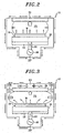
- the second radio frequency power 70 that is substantially not related to the plasma generation and the control of a plasma spatial distribution is omitted in Figs. 2 and 3 .
- the upper electrode 34 is attached to the chamber 10 via the ring-shaped insulator 35 and the rod-shaped inductor 54 is connected between the upper electrode 34 and the ground potential.
- the inductor 54 is detached, the upper electrode 34 is installed inside the processing chamber 10 in a DC-floating state.
- a plasma of the processing gas is generated in the processing space PS by a radio frequency discharge between the susceptor 16 and the upper electrode 34 and that between the susceptor 16 and the sidewall of the chamber 10.
- the plasma thus generated is diffused in all directions, especially in upward and radially outward directions. Electron current in the plasma flows toward the ground via the upper electrode 34, the sidewall of the chamber 10 or the like.
- the susceptor 16 As the frequency of the first radio frequency power increases, a radio frequency current is likely to be gathered at the central portion of the susceptor due to skin effect and the susceptor 16 is closer to the upper electrode 34 than the sidewall of the chamber 10, the upper electrode 34 and the sidewall of the chamber 10 having a same potential (ground potential). Accordingly, a larger amount of radio frequency power is discharged from the central portion of the electrode toward the processing space PS. Thus, most of the plasma electron current flows in the upper electrode 34, especially in the central portion thereof, while a considerably small part of the plasma electron current flows in the sidewall of the chamber 10. As a result, the plasma density spatial distribution in the central portion of the electrode is highest and significantly different from that in the edge portion of the electrode.
- an equivalent circuit for a radio frequency transmission line from a boundary surface between the processing space PS and the upper electrode 34 to the ground potential via the upper electrode 34 is represented by a circuit including a coil L 54 arranged parallel to capacitors C 35 and C 50 as shown in Fig. 3 .
- the coil L 54 is an inductance of the rod-shaped inductor 5 and 4 and specifically, the coil L 54 is connected in series with a resistance (not illustrated) of the rod-shaped inductor 54.
- the capacitor C 35 is a capacitance between the upper electrode 34 and the sidewall of the chamber 10 and mainly formed by the ring-shaped insulator 35.
- the capacitor C 50 is a capacitance between the upper electrode 34 and the ceiling of the chamber 10 and mainly formed by air in the gap 50.
- the plasma of the processing gas is generated in the processing space PS by a radio frequency discharge between the susceptor 16 and the upper electrode 34 and that between the susceptor 16 and the sidewall of the chamber 10.
- the plasma thus generated is diffused in upward and radially outward directions, and an electron current in the plasma flows toward the ground via the upper electrode 34, the sidewall of the chamber 10 or the like.
- a radio frequency current is likely to be gathered at the central portion of the susceptor.
- the susceptor 16 is located closer to the upper electrode 34 than the sidewall of the chamber 10.
- a parallel LC circuit 80 including the coil L 54 and the capacitors C 35 and C 50 is provided between the upper electrode 34 and the ground potential. Therefore, when the parallel LC circuit 80 provides a high impedance Z against the first radio frequency power, the radio frequency current hardly flows in the upper electrode 34 disposed directly above the susceptor 16 even though it is gathered at the central portion of the susceptor 16.
- a relatively increased part of the plasma electron current flows in the sidewall of the chamber 10, which makes the plasma density distribution widen radially.
- the impedance Z of the parallel LC circuit 80 it is possible to control a ratio of the electron current flowing between the susceptor 16 and the upper electrode 34 and that flowing between the susceptor 16 and the sidewall of the chamber 10 and further to control the plasma density spatial distribution characteristics to be uniform in a diametric direction.
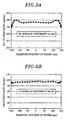
- Fig. 4 describes an example of frequency-impedance characteristics for a radio frequency transmission line from the boundary surface between the processing space PS and the upper electrode 34 to the ground potential via the upper electrode in the plasma etching apparatus.
- Fig. 4 describes an example of frequency-impedance characteristics for a radio frequency transmission line from the boundary surface between the processing space PS and the upper electrode 34 to the ground potential via the upper electrode in the plasma etching apparatus.
- an impedance X L that gradually increases with respect to the frequency is an organic reactance
- and an impedance X c that gradually decreases with respect to the frequency is a capacitive reactance
- the parallel LC circuit 80 causes a parallel resonance or an antiresonance at a frequency where the organic reactance X L becomes equal (absolute value) to the capacitive reactance X c .
- an impedance Z of the parallel LC circuit 80 has a maximum peak value at the antiresonance frequency f 0 .
- the antiresonance frequency f 0 appears within a range including the frequency of the first radio frequency power (preferably, from 5 MHz to 200 MHz). Accordingly, as illustrated in Fig. 4 , by selecting or setting a variable or selectable parameter, i.e., an inductance of the inductor 54 such that the antiresonance frequency f 0 appears near (preferably, at) the frequency (40 MHz) of the first radio frequency power, a high value Z 40 can be selected as the impedance Z of the parallel LC circuit 80 for the first radio frequency. Further, as shown in Fig.
- an impedance Z 80 of the parallel LC circuit 80 for the second radio frequency can be set to be a value Z 2 significantly smaller than the value Z 40 for the first radio frequency by setting the antiresonance frequency f 0 within the range from 5 MHz to 200 MHz.
- the upper electrode 34 can be grounded at a low impedance for the second radio frequency.
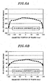
- FIGS. 5A and 5B illustrate, as a test example, in-surface distribution characteristics of etching rates of an oxide film SiO 2 and a photoresist PR by using the plasma etching apparatus of the first embodiment, respectively.
- an inductance of the inductor 54 is set to be about 400 nH and a combined capacitance of the capacitors C 35 and C 50 is set to be about 250 pF (low capacitance).
- Figs. 6A, 6B and 7A, 7B present comparative examples. Referring to Figs. 6A and 6B , there are illustrated, as a first comparative example, spatial distribution characteristics of the etching rates of the oxide film and the photoresist, respectively.
- the inductor 54 is omitted and a combined capacitance of the capacitors C 35 and C 50 is set to be about 20000 pH (high capacitance).
- a second comparative example spatial distribution characteristics of the etching rates of the oxide film and the PR, respectively.
- the inductor 54 is omitted and a combined capacitance of the capacitors C 35 and C 50 is set to be about 250 pH (low capacitance).
- the test example and the comparative examples have the following common etching conditions.
- etching rates of the oxide film and the PR are relatively uniform in a central portion of the wafer.
- the second comparative example where the inductor 54 is omitted and a ground capacitance of the upper electrode 34 is set to be a low capacitance of about 250 pF have significantly improved processing uniformity compared with the first comparative example.
- the etching rate of the oxide film in the central portion of the wafer is substantially same as that of the first comparative example, and the etching rate of the oxide film in the edge portion of the wafer increases compared with that of the first comparative example, which leads to improved in-surface uniformity of ⁇ 2.4 %.
- the etching rate of the photoresist increases compared with that of the first comparative example and becomes uniform in each portion of the wafer, which results in improved in-surface uniformity of ⁇ 4.4 %.
- the test example has further improved processing uniformity compared with the second comparative example, as can be seen from Figs. 5A and 5B .
- the etching rate of the oxide film increases in each portion of the wafer, especially in the edge portion, compared with that of the second comparative example, which results in significantly improved in-surface uniformity of ⁇ 1.2 %.
- the etching rate of the photoresist is substantially uniform in each portion of the wafer, which leads to improved in-surface uniformity of ⁇ 2.5 %.
- the etching rate distribution of the oxide film reflects an electron density distribution in plasma, i.e., a plasma density distribution.
- the etching rate distribution of the photoresist is affected by a dissociation of an initial gas by the plasma and thus more strongly depends on the plasma density distribution. Therefore, as can be seen from the test result of Figs. 5A and 5B , in accordance with the test example, the uniformity of the plasma density distribution is significantly improved by suppressing a concentration of the plasma generated in the processing space PS on the central portion of the electrode and broadening the plasma radially outwardly. As described above, the plasma density distribution can be considerably improved in the second comparative example compared with the first comparative example.
- the low-capacitance (250 pF) capacitors C 35 and C 50 forming the ground circuit of the upper electrode 34 provide a considerably great impedance to the second radio frequency (2 MHz) as well as the first radio frequency (40 MHz). More specifically, referring to Fig. 4 illustrating the frequency characteristics of the capacitive reactance X C , the impedance at the first radio frequency (40 MHz) is higher than that at the second radio frequency (2 MHz).
- the impedance of the ground circuit of the upper electrode 34 is high for the second radio frequency, the impact of ions incident on the upper electrode 34 due to the second radio frequency becomes weak, thereby deteriorating the sputtering effect.
- the inductor 54 is provided, so that an impedance of the parallel LC circuit 80 can be set to be high for the first radio frequency (40 MHz) and considerably low for the second radio frequency (2 MHz). Accordingly, the uniformity of the plasma density distribution can be significantly improved. Also, it is possible to maintain the impact intensity of ions incident on the upper electrode 34 and further the sputtering effect (electrode surface cleaning effects) sufficiently high.
- the main etching conditions were as follows:
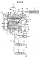
- Fig. 8 illustrates a configuration of a plasma etching apparatus in accordance with an embodiment of the present invention.
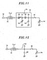
- the upper end of the inductor 54 is electrically connected with a variable DC power supply 84 via a DC filter unit 82 in the embodiment, while it is grounded via the conducting wire 56 in the example of figure 1 .
- the configurations and functions of the other components of the embodiment are same as those of the example of figure 1 .
- Fig. 9 shows an exemplary circuit configuration in the DC filter unit 82.
- the inductor 54 is connected in series with two coils 86 and 88 in a DC transmission line from the variable DC power supply 84 to the upper electrode 34. Further, capacitors 90 and 92 are respectively connected between a node N 1 and a ground potential and between a node N 2 and the ground potential, wherein the node N 1 is provided between the coils 86 and 88 and the node N 2 is provided between the coil 88 and the variable DC power supply 84.
- a serial-parallel LC circuit 94 is formed by the coils 86 and 88 and the capacitors 90 and 92.
- the DC filter unit 82 may have therein a cooling (blowing) device such as a fan so as to maintain the temperatures of electrical components or devices in the DC filter unit 82 at appropriate levels.
- a cooling (blowing) device such as a fan so as to maintain the temperatures of electrical components or devices in the DC filter unit 82 at appropriate levels.
- the DC filter unit 82 can be installed at any location between the inductor 54 and the variable DC power supply 84, it is preferable that the DC filter unit 82 is mounted on a ceiling (top surface) of the chamber 10.
- a DC voltage outputted from the variable DC power supply 84 is applied to the upper electrode 34 via the coils 86 and 88 of the serial-parallel LC circuit 94 and the inductor 54.
- the variable DC power supply 84 is configured to output a DC voltage having a polarity and a voltage level selected depending on processing types or conditions.
- sputtering effect deposit removal effect
- the generation amount of plasma is reduced by enlarging a plasma sheath with respect to the upper electrode 34
- electrons generated near the upper electrode 34 are irradiated onto a target substrate (semiconductor wafer W);
- a plasma potential can be controlled; (5) electron density (plasma density) is increased; and (6) the plasma density in the central portion is increased.
- an on/off switch 96 including, e.g., a relay switch between the variable DC power supply 84 and the serial-parallel LC circuit 94.
- the serial-parallel LC circuit 94 in the DC filter unit 82 allows the DC voltage from the variable DC power supply 84 to flow therethrough to the upper electrode 34 and generates a serial resonance at a low frequency range (preferably, from 100 kHz to 15 MHz) and a parallel resonance at a radio frequency range (preferably, from 5 MHz to 200 MHz) with respect to the radio frequency from the upper electrode 34.
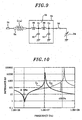
- Fig. 10 depicts, as an example, frequency-impedance characteristics Z 94 of the serial-parallel LC circuit 94 alone in this embodiment and frequency-impedance characteristics Z A in a radio frequency transmission line from a boundary surface between the processing space PS and the upper electrode 34 to the ground potential via the upper electrode 34.
- a resonance frequency and an antiresonance frequency of the serial-parallel LC circuit 94 are set to be about 2 MHz and about 45 MHz, respectively.
- the frequency-impedance characteristics Z 94 a considerably high impedance of about 1000 ⁇ corresponds to the first radio frequency (40 MHz), whereas an extremely low impedance of about 1 ⁇ corresponds to the second radio frequency (2 MHz).
- the frequency-impedance characteristics Z A of the entire ground circuit around the upper electrode 34 wherein the inductor 54, the capacitors C 35 , C 50 and the like are added to the serial-parallel LC circuit 94 the antiresonance frequency is shifted to the low frequency range up to about 10 MHz, whereas the resonance frequency is maintained near about 2 MHz.
- the impedance corresponding to the first radio frequency (40 MHz) is considerably reduced to about 20 ⁇
- the impedance corresponding to the second radio frequency (2 MHz) is slightly reduced to about 0.7 ⁇ , and the difference therebetween is still maintained more than 20 times.
- a noticeable point in Fig. 10 is that the impedance corresponding to the second radio frequency (2 MHz) in the frequency-impedance characteristics Z A of the entire ground circuit around the upper electrode 34 can be lowered to 1 ⁇ or less by utilizing a resonance phenomenon of the serial-parallel LC circuit 94.
- the upper electrode 34 is seemingly short-circuited to the ground potential (imaginary short-circuit state) in view of the second radio frequency (2 MHz), which enhances the impact intensity of ions incident on the upper electrode 34 due to the vibrations of the second radio frequency and further the sputtering effect (deposit removal effect).
- the frequency-impedance characteristics Z 94 and Z A shown in Fig. 10 are provided for illustrative purpose only and can be modified or adjusted by varying inductance values of the coils 86 and 88 and capacitance values of the capacitors 90 and 92 in the serial-parallel LC circuit 94. Further, the circuit configuration shown in Fig.
- the circuit network may be formed in T type, ⁇ type or the like without being limited to that shown in Fig. 9 .
- a circuit element having a different function e.g., a noise removing coil (not shown) or the like, may be inserted between the serial-parallel LC circuit 94 and the variable DC power supply 84.
- a variable impedance element may be provided in the DC filter unit 82. For example, as shown in Fig.
- the coil 86 and the capacitors 90 may be made to serve as a variable reactor and a variable capacitor, respectively.
- the upper electrode 34 instead of the serial-parallel LC circuit 94, the upper electrode 34 may be grounded via a serial LC circuit 100 including the inductor 54 and a capacitor 98, as shown in Fig. 12 .
- a serial-parallel LC circuit (not shown) in which the capacitors C 35 and C 50 (see, Fig. 3 ) are connected with the serial LC circuit 100 in parallel.
- an inductance of the inductor 54 and a capacitance of the capacitor 98 is preferred to be set such that a desired resonance frequency and a desired antiresonance frequency higher than the resonance frequency are obtained in respective frequency ranges, and preferably such that the resonance frequency is obtained near the frequency of the second radio frequency power.
- an output terminal of the variable DC power supply 84 is preferably electrically connected with a node N a provided between the inductor 54 and the capacitor 98, as shown in Fig. 12 .
- the variable DC power supply 84 may be omitted.
- the inductor 54 and the capacitor 98 may be exchanged with respect to the upper electrode 34.
- the capacitor 98 may be connected in series between the upper electrode 34 and the inductor 54.
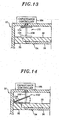
- the inductor 54 is not limited to a rod-shaped conductor and may be formed of a coil-shaped conductor or any inductive element or member for providing a capacitive impedance. Further, it is possible to vary an electrostatic capacitance or a ground capacitance around the upper electrode 34 in the plasma etching apparatus of the above embodiments.
- Figs. 13 to 15 show exemplary configurations of a capacitance varying unit. Capacitance varying units 102 and 102' shown in Figs.
- the manipulating mechanism 106 of Fig. 13 which is grounded directly or via the chamber, is made of a conductive material, a material conductive to a radio frequency, or a material having a low impedance to a radio frequency.
- a ground capacitance of the upper electrode 34 can be varied depending on the height positions of the conductive plates 104 and 104'. The closer the conductive plates 104 and 104' are to the ceiling surface of the chamber 10, the smaller the ground capacitance of the upper electrode 34 becomes. On the contrary, the closer the conductive plates 104 and 104' are to the top surface of the upper electrode 34, the grater the ground capacitance of the upper electrode 34 becomes. To be extreme, it is possible to make the ground capacitance infinite by allowing the upper electrode 34 to be grounded via the conductive plates 104 and 104' contacted therewith.
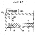
- a liquid Q having an appropriate dielectric constant for example, an organic solvent such as Galden or the like
- a liquid Q having an appropriate dielectric constant can be supplied from the outside of the chamber 10 into the liquid chamber 110 via a line 112 and removed therefrom.
- an electrostatic capacitance of the entire ring-shaped insulator 35 and further a ground capacitance of the upper electrode 34 can be varied.
- a variable capacitor (not shown) may be connected between the upper electrode 34 and the chamber 10.
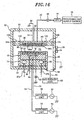
- any frequency-impedance characteristics can be realized by appropriately combining the variable capacitor, the capacitance varying unit 102, a variable inductance element (not shown) for varying an inductance of the inductor 54, the variable impedance element in the DC filter unit 82 shown in Fig. 11 and the like. More specifically, an impedance to the first radio frequency for plasma generation can be adjusted by the aforementioned variable capacitor or the capacitance varying unit 102, while an impedance to the second radio frequency for ion attraction can be adjusted by the variable impedance element in the DC filter unit 82. As another example, a configuration shown in Fig. 16 may be employed.
- the first radio frequency power is supplied from the radio frequency power supply 30 to the susceptor 16 via the matching unit 32 and the power feed rod 33 while the second radio frequency power is supplied from the radio frequency power supply 70 to the susceptor 16 via the matching unit 72 and the power feed rod 74 (the type in which dual frequency powers are applied to the lower electrode).
- the upper electrode is divided in a radial direction into a disk-shaped inner upper electrode 34A and a ring-shaped outer upper electrode 122.
- a ring-shaped insulator 120 is inserted between the inner upper electrode 34A and the outer upper electrode 122 and, also, a ring-shaped insulator 124 is inserted between the outer upper electrode 122 and the sidewall of the chamber 10.
- Such a configuration enables the first radio frequency power of a radio frequency to flow mainly in a path to the sidewall (earth) of the chamber 10 via the outer upper electrode 122 and the second radio frequency power of a low frequency to flow mainly in a path to the earth via the inner upper electrode 34A and the power feed rod 52.
- the frequencies of the first and the second radio frequency power are used as illustrative purpose only in the above embodiments, and any frequency can be selected depending on processes.
- the first radio frequency power for plasma generation has a frequency of about 13.56 MHz or greater
- the second radio frequency power for ion attraction to the substrate or the upper electrode has a frequency of about 13.56 MHz or less.
- the ground circuit around the upper electrode 34 in the aforementioned embodiments has been described for illustrative purpose only, and various modifications can be made to configurations and functions of the components of the apparatus.
- the above examples and embodiment have been described with respect to the plasma etching apparatus and method, the present disclosure may be applied to other parallel plate type plasma processing apparatus and method such as plasma chemical vapor deposition (CVD), plasma oxidation, plasma nitridation, sputtering and the like.
- the substrate to be processed is not limited to the semiconductor wafer, but it may be a flat panel display substrate, a photo mask, a compact disk (CD) substrate, a printed substrate or the like. While the invention has been shown and described with respect to the embodiment, it will be understood by those skilled in the art that various changes and modification may be made without departing from the scope of the invention which is defined in the following claims.
Landscapes
- Physics & Mathematics (AREA)
- Engineering & Computer Science (AREA)
- Plasma & Fusion (AREA)
- Chemical & Material Sciences (AREA)
- Analytical Chemistry (AREA)
- Plasma Technology (AREA)
- Drying Of Semiconductors (AREA)
- Physical Vapour Deposition (AREA)
Description
- The present invention relates to a technique for performing a plasma processing on a target substrate; and, more particularly, to a capacitively coupled plasma processing apparatus of a dual frequency application mode and a plasma processing method.
- In a manufacturing process of semiconductor devices or flat panel displays (FPDs), a plasma is used to perform a processing, such as etching, deposition, oxidation, sputtering or the like, so as to obtain a good reaction of a processing gas at a relatively low temperature. Conventionally, a capacitively coupled type plasma apparatus has been widely employed as a single-wafer plasma processing apparatus, especially, as a single-wafer plasma etching apparatus.
Generally, in the capacitively coupled plasma processing apparatus, an upper electrode and a lower electrode are disposed to face each other in parallel in a vacuum processing chamber, a substrate to be processed (a semiconductor wafer, a glass substrate or the like) is mounted on the upper electrode, and a radio frequency voltage is applied to either one of the upper and the lower electrode. Electrons are accelerated by an electric field formed by the radio frequency voltage to collide with a processing gas. As a result of ionization by the collision between the electrons and the processing gas, a plasma is generated, and a desired microprocessing (for example, etching) is performed on the surface of the substrate by radicals or ions in the plasma. At this time, the electrode to which the radio frequency voltage is applied is connected with a radio frequency power supply via a blocking capacitor in a matching unit and thus serves as a cathode. A cathode coupling method in which the radio frequency voltage is applied to the lower electrode, serving as the cathode, for supporting the substrate enables an anisotropic etching by substantially vertically attracting ions in the plasma to the substrate with a self-bias voltage generated in the lower electrode.
In the capacitively coupled plasma processing apparatus of the dual frequency application type, a first radio frequency power of a relatively radio frequency (generally, 27 MHz or greater) for plasma generation and a second radio frequency power of a relatively low frequency (generally, 13.56 MHz or less) for ion attraction are applied to the lower electrode (see, e.g., Japanese Patent Laid-open Publication No.2000-156370 U.S. Patent No. 6,642,149 ).
The dual frequency application is advantageous in that plasma density and anisotropic etching selectivity can be individually optimized by the first and the second radio frequency power, and also in that the second radio frequency power of a relatively low frequency can effectively prevent or suppress a deposit adhesion during a process in which deposits such as polymer and the like are adhered to an upper electrode. Specifically, when the ions are incident on the upper electrode serving as an anode, a deposited film (and an oxide film, if it exists) adhered to the electrode is sputtered by ion impact. The number of ions used for the sputtering is determined by the first radio frequency. Further, an electric field that accelerates the ions is generated by the second radio frequency power of the relatively low frequency. - In the conventional capacitively coupled plasma processing apparatus of the dual frequency application type as described above, the upper electrode serving as the anode to which no radio frequency is applied is DC-grounded generally. Typically, a processing chamber, which is frame grounded, is formed of metal, e.g., aluminum, a stainless steel or the like, so that the upper electrode can be held at ground potential via the processing chamber. Accordingly, the upper electrode is directly attached to a ceiling of the processing chamber to be integrally assembled thereto or the ceiling of the processing chamber itself is used as the upper electrode.
With a recent trend of miniaturization of design rules for the manufacturing process, a high-density plasma is required to be available at a low pressure for a plasma processing. In the capacitively coupled plasma processing apparatus in which dual frequency powers are applied to the lower electrode, the frequency of the first radio frequency power, which mainly contributes to a plasma generation, tends to be gradually increased and a frequency of 40 MHz or greater is standardly used in recent years. However, if the frequency of the radio frequency power becomes high, a radio frequency current is made to be concentrated on a central portion of the electrode, so that a density of a plasma generated in a processing space between two electrodes becomes higher at the central portion of the electrode than that at the edge portion thereof. As a result, there occurs a problem that process characteristics become nonuniform in a radial direction. Meanwhile, since the frequency of the second frequency power that mainly contributes to ion attraction is relatively low, it is not focused on the central portion of the electrode. In other words, in the conventional apparatus in which the upper electrode is directly attached to or formed integral with the processing chamber to be DC-grounded therethrough, the functions of the second radio frequency power that include attracting the ions toward the substrate and suppressing the deposit adhesion to the upper electrode are not deteriorated. - In
US 2006/0037704 A1 there is disclosed a plasma processing apparatus for processing a substrate by using a plasma which includes a processing chamber for accommodating and processing the substrate, a lower electrode for mounting the substrate thereon in the processing chamber, an upper electrode disposed to face the lower electrode in the processing chamber, a radio frequency supply for supplying a radio frequency power to at least one of the lower and upper electrodes, to thereby generate the plasma between the lower and upper electrodes, and an electrical characteristic control unit for adjusting an impedance of a circuit at the side of an electrode to the plasma for a frequency of at least one radio frequency wave present in the processing chamber such that the circuit does not resonate. - In
WO 03/003405 - It is, therefore, an object of the present invention to provide a capacitively coupled plasma processing apparatus and method of a dual frequency application type in which two kinds of radio frequency powers are applied to an electrode for supporting a target substrate thereon, wherein in-surface uniformity of processes can be improved by controlling plasma density spatial distribution characteristics while preventing or suppressing an undesired film from being formed on another electrode facing the electrode for supporting the target substrate.
- In accordance with a first aspect of the invention, there is provided a plasma processing apparatus according to
claim 1. - In accordance with a second aspect of the invention, there is provided a plasma processing method according to claim 11.
- According to the disclosure, an equivalent circuit in a radio frequency transmission line from the boundary surface between the processing space and the first electrode to the ground potential via the first electrode is configured as a serial-parallel LC circuit. In this serial-parallel LC circuit, an impedance extremely decreases at a specific frequency (resonance frequency) and extremely increases at another specific frequency (antiresonance frequency). By utilizing those characteristics, a high impedance and a low impedance can be obtained at the first and the second radio frequency, respectively. The resonance frequency is obtained within a range from about 0.1 kHz to about 15 MHz and the antiresonance frequency is obtained within a range from about 5 MHz to about 200 MHz in the frequency-impedance characteristics of the equivalent circuit or the serial-parallel LC circuit. By optimally increasing the impedance at the first radio frequency in the serial-parallel LC circuit, plasma density spatial distribution characteristics can be controlled to be uniform diametrically. Further, by decreasing the impedance at the second radio frequency in the serial-parallel LC circuit substantially to a level at which a short-circuit occurs, the sputtering effect of removing an undesired film from the surface of the first electrode can be further enhanced.
- In the plasma processing apparatus in accordance with the first aspect of the present invention, a desired DC voltage is applied from the DC power supply to the first electrode via the filter to obtain acting effects thereby. Further, the functions of the first and the second radio frequency can be corrected, controlled or assisted by the frequency-impedance characteristics of the filter. For example, when the filter is provided in the serial-parallel LC circuit as in the second plasma processing apparatus, it is possible to improve the plasma density spatial distribution characteristics or the sputtering effect for the first electrode (which removes an undesired film therefrom).
In accordance with the plasma processing apparatus and the plasma processing method of the present invention, it is possible to resolve a tradeoff in the functions of the first and the second radio frequency in the capacitively coupled apparatus of a dual frequency application type (wherein two radio frequency powers are applied to an electrode) with the above-described configurations and operations. Especially, the in-surface uniformity of processes can be improved by controlling the plasma density spatial distribution characteristics while preventing or suppressing an undesired film from being formed on the other electrode facing the electrode to which two radio frequency powers are applied. - The above and other objects and features of the present invention will become apparent from the following description, given in conjunction with the accompanying drawings, in which:
-
Fig. 1 is a vertical cross sectional view of a plasma etching apparatus in accordance with an example; -
Fig. 2 schematically shows a capacitively coupled radio frequency discharge system in a plasma etching apparatus of a comparative example; -
Fig. 3 schematically illustrates a capacitively coupled radio frequency discharge system in the plasma etching apparatus shown inFig. 1 ; -
Fig. 4 describes an example of frequency-impedance characteristics in a radio frequency transmission line to a ground potential via an upper electrode in the plasma etching apparatus shown inFig. 1 ; -
Fig. 5A depicts in-surface distribution characteristics of an etching rate of an oxide film in a test example; -
Fig. 5B presents in-surface distribution characteristics of an etching rate of a photoresist in the test example; -
Fig. 6A represents in-surface distribution characteristics of an etching rate of an oxide film in a first comparative example; -
Fig. 6B describes in-surface distribution characteristics of an etching rate of a photoresist in the first comparative example; -
Fig. 7A offers in-surface distribution characteristics of an etching rate of an oxide film in a second comparative example; -
Fig. 7B provides in-surface distribution characteristics of an etching rate of a photoresist in the second comparative example; -
Fig. 8 illustrates a vertical cross sectional view of a plasma etching apparatus in accordance with an embodiment of the present invention; -
Fig. 9 is a circuit diagram showing an exemplary configuration of a circuit in a DC filter unit of the plasma etching apparatus; -
Fig. 10 depicts an example of frequency-impedance characteristics of a serial-parallel LC circuit in the DC filter unit and an example of frequency-impedance characteristics in a radio frequency transmission line to a ground potential via an upper electrode in the plasma etching apparatus shown inFig. 2 ; -
Fig. 11 shows a circuit diagram of a modified configuration of the circuit in the DC filter unit; -
Fig. 12 sets forth a circuit diagram of a modification of the serial-parallel LC circuit ; -
Fig. 13 describes a fragmentary cross sectional view of an example of a capacitance varying unit in the plasma etching apparatus in accordance with the embodiment of the present invention; -
Fig. 14 offers a fragmentary cross sectional view of another example of the capacitance varying unit in the plasma etching apparatus in accordance with the embodiment of the present invention; -
Fig. 15 presents a fragmentary cross sectional view of still another example of the capacitance varying unit in the plasma etching apparatus in accordance with the embodiment of the present invention; and -
Fig. 16 represents a vertical cross sectional view of a plasma etching apparatus in accordance with an example. - Hereinafter, examples and embodiments will be described with reference to the accompanying drawings.
Fig. 1 illustrates a configuration of a plasma processing apparatus in accordance with an example. The plasma processing apparatus is configured as a capacitively coupled (parallel plate type) plasma processing apparatus of a type in which dual frequency powers are applied to a lower electrode. The plasma processing apparatus has a cylindrical vacuum chamber (processing chamber) 10 made of, e.g., an aluminum whose surface is alumite-treated (anodically oxidized), and thechamber 10 is frame grounded.
Acylindrical susceptor support 14 is provided at a bottom portion in thechamber 10 via aninsulation plate 12 made of ceramic or the like. Further, asusceptor 16 made of, e.g., aluminum, is disposed above thesusceptor support 14. Thesusceptor 16 serves as a lower electrode and a target substrate, e.g., a semiconductor wafer W, is mounted thereon.
On the top surface of thesusceptor 16, there is disposed anelectrostatic chuck 18 for attracting and holding the semiconductor wafer with an electrostatic adsorptive force. Theelectrostatic chuck 18 includes anelectrode 20 formed of a conductive film which is inserted between a pair of insulating layers or sheets. A DC power supply 22 is connected to theelectrode 20. Theelectrostatic chuck 18 is allowed to attract and hold the semiconductor wafer W thereon with a Coulomb force generated by a DC voltage applied from the DC power supply 22 thereto. Afocus ring 24 made of, e.g., silicon is disposed to surround theelectrostatic chuck 18 to improve an etching uniformity. Further, aninner wall member 25 made of, e.g., quartz is attached to the side surfaces of thesusceptor 16 and thesusceptor support 14.
Acoolant path 26 is circumferentially provided inside thesusceptor support 14. A coolant, e.g., cooling water, of a specific temperature is supplied into and circulated along thecoolant path 26 from an external chiller unit (not shown) viacoolant lines susceptor 16 can be controlled by the temperature of the coolant. Further, a thermally conductive gas, e.g., He gas, is supplied into a gap between the top surface of the electrostatic chuck and the backside of the semiconductor wafer W from a thermally conductive gas supply unit (not shown) via agas supply line 28.
Thesusceptor 16 is electrically connected with a first and a second radiofrequency power supply units power feed rods frequency power supply 30 outputs a radio frequency power of a specific frequency, e.g., 40 MHz, for plasma generation. Meanwhile, the second radiofrequency power supply 70 outputs a radio frequency power of a specific frequency, e.g., 2 MHz, which mainly contributes to ion attraction toward the semiconductor wafer W on the susceptor and to prevention of an adhesion of an undesired film such as a deposited film, an oxide film or the like to anupper electrode 34 and removal of the undesired film which will be described later.
Theupper electrode 34 is provided above thesusceptor 16 to face thesusceptor 16 in parallel. Further, theupper electrode 34 has anelectrode plate 36 having a plurality ofgas injection openings 36a and anelectrode support 38 for detachably holding theelectrode plate 36, theelectrode plate 36 being made of a semiconductor material, e.g., Si, SiC or the like, theelectrode support 38 being made of a conductive material, e.g., aluminum whose surface is alumite-treated. Theupper electrode 34 is attached in an electrically floating state to thechamber 10 via a ring-shapedinsulator 35. A plasma generation space or a processing space PS is defined by theupper electrode 34, thesusceptor 16 and the sidewall of thechamber 10. The ring-shapedinsulator 35, which is made of, e.g., alumina (Al2O3), is attached so that a gap between an outer peripheral surface of theupper electrode 34 and the sidewall of thechamber 10 can be airtightly sealed. The ring-shapedinsulator 35 physically holds theupper electrode 34 and electrically forms a part of capacitance between theupper electrode 34 and thechamber 10.
Theelectrode support 38 has therein agas buffer space 40 and also has on its bottom surface a plurality ofgas ventholes 38a extending from thegas buffer space 40 to communicate with thegas injection openings 36a of theelectrode plate 36. Thegas buffer space 40 is connected with a processinggas supply source 44 via agas supply line 42, and a massflow controller MFC 46 and an opening/closingvalve 48 are provided in thegas supply line 42. When a specific processing gas is introduced from the processinggas supply source 44 into thegas buffer space 40, the processing gas is injected into the processing space PS toward the semiconductor wafer W on thesusceptor 16 in a shower shape from thegas injection openings 36a of theelectrode plate 36. So, theupper electrode 34 also serves as a shower head for supplying a processing gas into the processing space PS.
Further, theelectrode support 38 has therein a passageway (not shown) through which a coolant, e.g., cooling water, flows, so that a temperature of the entireupper electrode 34, particularly theelectrode plate 36, can be controlled to a specific level with the coolant supplied from an external chiller unit. In order to further stabilize the temperature control of theupper electrode 34, a heater (not shown) including, e.g., a resistance heating element may be attached to an inside or a top surface of the electrode support 39.
A hollow space orgap 50 is provided between the top surface of theupper electrode 34 and the ceiling of thechamber 10. Further, a through-hole 52 is formed in a central portion of the top surface of thechamber 10, and a rod-shapedinductor 54 is vertically extended in thegap 50 and the through-hole 52. The rod-shapedinductor 54 has a lower end directly connected with the central portion of the top surface of theupper electrode 34 and an upper end connected with a ground potential (generally, the chamber 10) via a conducting wire. Alternatively, the upper end of the rod-shapedinductor 54 may be directly connected to the ceiling of theupper electrode 34.
An annular space defined by thesusceptor 16, thesusceptor support 14 and the sidewall of thechamber 10 serves as a gas exhaust space. Agas exhaust port 58 of thechamber 10 is provided at a bottom of the gas exhaust space. Agas exhaust unit 62 is connected with thegas exhaust port 58 via agas exhaust line 60. Thegas exhaust unit 62 has a vacuum pump such as a turbo molecular pump or the like, so that the inside of thechamber 10, especially the processing space PS, can be depressurized to a required vacuum level. Moreover, attached to the sidewall of thechamber 10 is agate valve 66 for opening and closing a loading/unloadingport 64 for the semiconductor wafer W.
In the plasma etching apparatus, in order to perform an etching process, thegate valve 66 is opened and a semiconductor wafer W to be processed is loaded into thechamber 10 to be mounted on theelectrostatic chuck 18. Then, a specific processing gas, i.e., an etching gas (generally, a gaseous mixture) is supplied into thechamber 10 from the processinggas supply source 44 at a specified flow rate and flow rate ratio, while thechamber 10 is evacuated by thegas exhaust unit 62 such that the internal pressure of thechamber 10 is maintained at a specific vacuum level. Further, a first radio frequency power (about 2 MHz) and a second radio frequency power (about 40 MHz) are concurrently applied to the susceptor 16 from the first and the second radiofrequency power supply electrode 20 of theelectrostatic chuck 18 from theDC power supply 46, whereby the semiconductor wafer W is firmly fixed on theelectrostatic chuck 18. The etching gas injected from theupper electrode 34 as the shower head is converted into a plasma by a radio frequency discharge in the plasma space PS, and films formed on the main surface of the semiconductor wafer W are etched by radicals or ions present in the plasma.
In such a capacitively coupled plasma etching apparatus, by applying to the susceptor (lower electrode) 16 a first radio frequency power of a relatively radio frequency, e.g., 40 MHz, suitable for plasma generation, a high-density plasma in a desirable dissociated state can be generated even at a low pressure. Also, by applying to the susceptor 16 a second radio frequency power of a relatively low frequency, e.g., 2 MHz, suitable for ion attraction, it is possible to perform an anisotropic etching having high selectivity to the semiconductor wafer W on theelectrostatic chuck 18. Further, it is also possible to remove a deposited film or an oxide film on the upper electrode 34 (electrode surface cleaning) by the ions incident thereon or the sputtering.
Hereinafter, features of the plasma etching apparatus in accordance with the example will be described with reference toFigs. 2 to 4 . For convenience, the secondradio frequency power 70 that is substantially not related to the plasma generation and the control of a plasma spatial distribution is omitted inFigs. 2 and 3 .
As described above, in the plasma etching apparatus, theupper electrode 34 is attached to thechamber 10 via the ring-shapedinsulator 35 and the rod-shapedinductor 54 is connected between theupper electrode 34 and the ground potential. In other words, if theinductor 54 is detached, theupper electrode 34 is installed inside theprocessing chamber 10 in a DC-floating state.
First of all, as for a comparative example, there will be described a case where theupper electrode 34 is directly attached to thechamber 10 to be DC-connected with the ground potential, for example. In this case, as shown inFig. 2 , when the first radio frequency power from the radiofrequency power supply 30 is applied to thesusceptor 16, a plasma of the processing gas is generated in the processing space PS by a radio frequency discharge between the susceptor 16 and theupper electrode 34 and that between the susceptor 16 and the sidewall of thechamber 10. The plasma thus generated is diffused in all directions, especially in upward and radially outward directions. Electron current in the plasma flows toward the ground via theupper electrode 34, the sidewall of thechamber 10 or the like. In thesusceptor 16, as the frequency of the first radio frequency power increases, a radio frequency current is likely to be gathered at the central portion of the susceptor due to skin effect and thesusceptor 16 is closer to theupper electrode 34 than the sidewall of thechamber 10, theupper electrode 34 and the sidewall of thechamber 10 having a same potential (ground potential). Accordingly, a larger amount of radio frequency power is discharged from the central portion of the electrode toward the processing space PS. Thus, most of the plasma electron current flows in theupper electrode 34, especially in the central portion thereof, while a considerably small part of the plasma electron current flows in the sidewall of thechamber 10. As a result, the plasma density spatial distribution in the central portion of the electrode is highest and significantly different from that in the edge portion of the electrode.
In contrast, in the example offigure 1 in which theupper electrode 34 is attached to thechamber 10 in a DC-floating state and connected with the ground potential via the rod-shapedinductor 54, an equivalent circuit for a radio frequency transmission line from a boundary surface between the processing space PS and theupper electrode 34 to the ground potential via theupper electrode 34 is represented by a circuit including a coil L54 arranged parallel to capacitors C35 and C50 as shown inFig. 3 . The coil L54 is an inductance of the rod-shaped inductor 5 and 4 and specifically, the coil L54 is connected in series with a resistance (not illustrated) of the rod-shapedinductor 54. The capacitor C35 is a capacitance between theupper electrode 34 and the sidewall of thechamber 10 and mainly formed by the ring-shapedinsulator 35. The capacitor C50 is a capacitance between theupper electrode 34 and the ceiling of thechamber 10 and mainly formed by air in thegap 50.
In this case as well, as similarly to the case shown inFig. 2 , when the first radio frequency power from the radiofrequency power supply 30 is applied to thesusceptor 16, the plasma of the processing gas is generated in the processing space PS by a radio frequency discharge between the susceptor 16 and theupper electrode 34 and that between the susceptor 16 and the sidewall of thechamber 10. The plasma thus generated is diffused in upward and radially outward directions, and an electron current in the plasma flows toward the ground via theupper electrode 34, the sidewall of thechamber 10 or the like. In thesusceptor 16, a radio frequency current is likely to be gathered at the central portion of the susceptor. Also, thesusceptor 16 is located closer to theupper electrode 34 than the sidewall of thechamber 10. However, aparallel LC circuit 80 including the coil L54 and the capacitors C35 and C50 is provided between theupper electrode 34 and the ground potential. Therefore, when theparallel LC circuit 80 provides a high impedance Z against the first radio frequency power, the radio frequency current hardly flows in theupper electrode 34 disposed directly above thesusceptor 16 even though it is gathered at the central portion of thesusceptor 16. Accordingly, a relatively increased part of the plasma electron current flows in the sidewall of thechamber 10, which makes the plasma density distribution widen radially. Theoretically, depending on the impedance Z of theparallel LC circuit 80, it is possible to control a ratio of the electron current flowing between the susceptor 16 and theupper electrode 34 and that flowing between the susceptor 16 and the sidewall of thechamber 10 and further to control the plasma density spatial distribution characteristics to be uniform in a diametric direction.
Fig. 4 describes an example of frequency-impedance characteristics for a radio frequency transmission line from the boundary surface between the processing space PS and theupper electrode 34 to the ground potential via the upper electrode in the plasma etching apparatus. InFig. 4 , an impedance XL that gradually increases with respect to the frequency is an organic reactance |jωL 54| of the coil L54, and an impedance Xc that gradually decreases with respect to the frequency is a capacitive reactance |1/jω(C35 +C50)| of the capacitors C35 and C50- Theoretically, theparallel LC circuit 80 causes a parallel resonance or an antiresonance at a frequency where the organic reactance XL becomes equal (absolute value) to the capacitive reactance Xc. Further, as shown inFig. 4 , an impedance Z of theparallel LC circuit 80 has a maximum peak value at the antiresonance frequency f0. It is preferable that the antiresonance frequency f0 appears within a range including the frequency of the first radio frequency power (preferably, from 5 MHz to 200 MHz).
Accordingly, as illustrated inFig. 4 , by selecting or setting a variable or selectable parameter, i.e., an inductance of theinductor 54 such that the antiresonance frequency f0 appears near (preferably, at) the frequency (40 MHz) of the first radio frequency power, a high value Z40 can be selected as the impedance Z of theparallel LC circuit 80 for the first radio frequency.
Further, as shown inFig. 4 , it is important that an impedance Z80 of theparallel LC circuit 80 for the second radio frequency can be set to be a value Z2 significantly smaller than the value Z40 for the first radio frequency by setting the antiresonance frequency f0 within the range from 5 MHz to 200 MHz. In other words, theupper electrode 34 can be grounded at a low impedance for the second radio frequency. As a consequence, the ions in the plasma which vibrate due to the second radio frequency are incident on theelectrode plate 36 of theupper electrode 34 with a strong impact, thereby sputtering (removing) a deposited film or an oxide film attached on the surface of theelectrode plate 36.
Figs. 5A and 5B illustrate, as a test example, in-surface distribution characteristics of etching rates of an oxide film SiO2 and a photoresist PR by using the plasma etching apparatus of the first embodiment, respectively. In this test example, an inductance of theinductor 54 is set to be about 400 nH and a combined capacitance of the capacitors C35 and C50 is set to be about 250 pF (low capacitance). Meanwhile,Figs. 6A, 6B and7A, 7B present comparative examples. Referring toFigs. 6A and 6B , there are illustrated, as a first comparative example, spatial distribution characteristics of the etching rates of the oxide film and the photoresist, respectively. In the first comparative example; theinductor 54 is omitted and a combined capacitance of the capacitors C35 and C50 is set to be about 20000 pH (high capacitance). Further, referring toFigs. 7A and 7B , there are illustrated, as a second comparative example, spatial distribution characteristics of the etching rates of the oxide film and the PR, respectively. In the second comparative example, theinductor 54 is omitted and a combined capacitance of the capacitors C35 and C50 is set to be about 250 pH (low capacitance). The test example and the comparative examples have the following common etching conditions.
Wafer diameter: 300 mm
Flow rates of processing gases:
C4F6/C4F8/Ar/O2 = 40/20/500/60 sccm
Pressure in chamber: 30 mTorr
Radio frequency power: 40 MHz/2 MHz = 2500/3200 W
Temperature of upper electrode: 60 °C - As can be seen from
Figs. 6A and 6B , in the first comparative example where theinductor 54 is omitted and a ground capacitance of theupper electrode 34 is set to be a high capacitance of about 20000 pF, the etching rates of the oxide film and the PR are relatively uniform in a central portion of the wafer. However, the etching rates thereof abruptly decrease near an edge portion of the wafer (R = ± 120 mm), which results in poor in-surface uniformity of ± 4.1 % and ± 19.1 %.
Meanwhile, as shown inFigs. 7A and 7B , the second comparative example where theinductor 54 is omitted and a ground capacitance of theupper electrode 34 is set to be a low capacitance of about 250 pF have significantly improved processing uniformity compared with the first comparative example. Specifically, the etching rate of the oxide film in the central portion of the wafer is substantially same as that of the first comparative example, and the etching rate of the oxide film in the edge portion of the wafer increases compared with that of the first comparative example, which leads to improved in-surface uniformity of ± 2.4 %. Moreover, the etching rate of the photoresist increases compared with that of the first comparative example and becomes uniform in each portion of the wafer, which results in improved in-surface uniformity of ± 4.4 %.
On the other hand, the test example has further improved processing uniformity compared with the second comparative example, as can be seen fromFigs. 5A and 5B . Specifically, the etching rate of the oxide film increases in each portion of the wafer, especially in the edge portion, compared with that of the second comparative example, which results in significantly improved in-surface uniformity of ± 1.2 %. Further, the etching rate of the photoresist is substantially uniform in each portion of the wafer, which leads to improved in-surface uniformity of ± 2.5 %.
In general, the etching rate distribution of the oxide film reflects an electron density distribution in plasma, i.e., a plasma density distribution. Further, the etching rate distribution of the photoresist is affected by a dissociation of an initial gas by the plasma and thus more strongly depends on the plasma density distribution. Therefore, as can be seen from the test result ofFigs. 5A and 5B , in accordance with the test example, the uniformity of the plasma density distribution is significantly improved by suppressing a concentration of the plasma generated in the processing space PS on the central portion of the electrode and broadening the plasma radially outwardly.
As described above, the plasma density distribution can be considerably improved in the second comparative example compared with the first comparative example. However, in the second comparative example in which theinductor 54 is not provided, the low-capacitance (250 pF) capacitors C35 and C50 forming the ground circuit of theupper electrode 34 provide a considerably great impedance to the second radio frequency (2 MHz) as well as the first radio frequency (40 MHz). More specifically, referring toFig. 4 illustrating the frequency characteristics of the capacitive reactance XC, the impedance at the first radio frequency (40 MHz) is higher than that at the second radio frequency (2 MHz). When the impedance of the ground circuit of theupper electrode 34 is high for the second radio frequency, the impact of ions incident on theupper electrode 34 due to the second radio frequency becomes weak, thereby deteriorating the sputtering effect.
To that end, in the test example, theinductor 54 is provided, so that an impedance of theparallel LC circuit 80 can be set to be high for the first radio frequency (40 MHz) and considerably low for the second radio frequency (2 MHz). Accordingly, the uniformity of the plasma density distribution can be significantly improved. Also, it is possible to maintain the impact intensity of ions incident on theupper electrode 34 and further the sputtering effect (electrode surface cleaning effects) sufficiently high.
As a result of measuring deposition rates of deposited films on a surface of theupper electrode 34 by using as an etching gas C4F8 gas generating a large amount of polymer in the test example and the second comparative example, the deposition rates of 80 nm/5 min and -100 nm/5 min were obtained in the test example and the second comparative example, respectively. In this measurement, the main etching conditions were as follows: - Flow rates of processing gases: C4F6/Ar = 5/1000 sccm
- Pressure in chamber: 40 mTorr
- Radio frequency power: 40 MHz/2 MHz = 2000/400 W
- Temperature: upper electrode/chamber sidewall/lower electrode = 150/150/40 °C
- Etching time: 5 min
- Consequently, it has been found that the deposited film is accumulated on the surface of the
upper electrode 34 in the second comparative example, whereas it is efficiently removed therefrom in the etching mode in the test example.
Fig. 8 illustrates a configuration of a plasma etching apparatus in accordance with an embodiment of the present invention. The upper end of theinductor 54 is electrically connected with a variableDC power supply 84 via aDC filter unit 82 in the embodiment, while it is grounded via theconducting wire 56 in the example offigure 1 . The configurations and functions of the other components of the embodiment are same as those of the example offigure 1 .
Fig. 9 shows an exemplary circuit configuration in theDC filter unit 82. In theDC filter unit 82 of this embodiment, theinductor 54 is connected in series with twocoils DC power supply 84 to theupper electrode 34. Further,capacitors coils coil 88 and the variableDC power supply 84. A serial-parallel LC circuit 94 is formed by thecoils capacitors
Moreover, theDC filter unit 82 may have therein a cooling (blowing) device such as a fan so as to maintain the temperatures of electrical components or devices in theDC filter unit 82 at appropriate levels. Although theDC filter unit 82 can be installed at any location between theinductor 54 and the variableDC power supply 84, it is preferable that theDC filter unit 82 is mounted on a ceiling (top surface) of thechamber 10.
A DC voltage outputted from the variableDC power supply 84 is applied to theupper electrode 34 via thecoils parallel LC circuit 94 and theinductor 54. Meanwhile, when the first and the second radio frequency power applied from the respective radiofrequency power supplies susceptor 16 are introduced to theupper electrode 34 via the processing space PS, they flow to the ground via theinductor 54 and the serial-parallel LC circuit 94 in theDC filter unit 82 while hardly flowing to the variableDC power supply 84.
The variableDC power supply 84 is configured to output a DC voltage having a polarity and a voltage level selected depending on processing types or conditions. It has been known that, by applying a proper DC voltage to theupper electrode 34, at least one of following effects can be obtained: (1) sputtering effect (deposit removal effect) on theupper electrode 34 is enhanced by increasing an absolute value of a self-bias voltage of theupper electrode 34; (2) the generation amount of plasma is reduced by enlarging a plasma sheath with respect to theupper electrode 34; (3) electrons generated near theupper electrode 34 are irradiated onto a target substrate (semiconductor wafer W); (4) a plasma potential can be controlled; (5) electron density (plasma density) is increased; and (6) the plasma density in the central portion is increased. For a case where it is not required to apply a DC voltage to be applied to theupper electrode 34, it is preferable to provide an on/offswitch 96 including, e.g., a relay switch between the variableDC power supply 84 and the serial-parallel LC circuit 94.
In the embodiment, the serial-parallel LC circuit 94 in theDC filter unit 82 allows the DC voltage from the variableDC power supply 84 to flow therethrough to theupper electrode 34 and generates a serial resonance at a low frequency range (preferably, from 100 kHz to 15 MHz) and a parallel resonance at a radio frequency range (preferably, from 5 MHz to 200 MHz) with respect to the radio frequency from theupper electrode 34. By utilizing such frequency-impedance characteristics of the serial-parallel LC circuit 94, it is possible to further improve the individual functions of the first and the second radio frequency in the dual frequency application type wherein two radio frequency powers are applied to the lower electrode.
Fig. 10 depicts, as an example, frequency-impedance characteristics Z94 of the serial-parallel LC circuit 94 alone in this embodiment and frequency-impedance characteristics ZA in a radio frequency transmission line from a boundary surface between the processing space PS and theupper electrode 34 to the ground potential via theupper electrode 34.
As shown inFig. 10 , in this example, a resonance frequency and an antiresonance frequency of the serial-parallel LC circuit 94 are set to be about 2 MHz and about 45 MHz, respectively. In the frequency-impedance characteristics Z94, a considerably high impedance of about 1000 Ω corresponds to the first radio frequency (40 MHz), whereas an extremely low impedance of about 1 Ω corresponds to the second radio frequency (2 MHz). In the frequency-impedance characteristics ZA of the entire ground circuit around theupper electrode 34 wherein theinductor 54, the capacitors C35, C50 and the like are added to the serial-parallel LC circuit 94, the antiresonance frequency is shifted to the low frequency range up to about 10 MHz, whereas the resonance frequency is maintained near about 2 MHz. Further, while the impedance corresponding to the first radio frequency (40 MHz) is considerably reduced to about 20 Ω, the impedance corresponding to the second radio frequency (2 MHz) is slightly reduced to about 0.7 Ω, and the difference therebetween is still maintained more than 20 times.
A noticeable point inFig. 10 is that the impedance corresponding to the second radio frequency (2 MHz) in the frequency-impedance characteristics ZA of the entire ground circuit around theupper electrode 34 can be lowered to 1 Ω or less by utilizing a resonance phenomenon of the serial-parallel LC circuit 94. As a consequence, theupper electrode 34 is seemingly short-circuited to the ground potential (imaginary short-circuit state) in view of the second radio frequency (2 MHz), which enhances the impact intensity of ions incident on theupper electrode 34 due to the vibrations of the second radio frequency and further the sputtering effect (deposit removal effect).
The frequency-impedance characteristics Z94 and ZA shown inFig. 10 are provided for illustrative purpose only and can be modified or adjusted by varying inductance values of thecoils capacitors parallel LC circuit 94.
Further, the circuit configuration shown inFig. 9 is provided for illustrative purpose only, and a modification can be made in or around theDC filter unit 82. For example, in the serial-parallel LC circuit 94, the number of coils and capacitors may be changed, the circuit network may be formed in T type, π type or the like without being limited to that shown inFig. 9 . Besides, a circuit element having a different function, e.g., a noise removing coil (not shown) or the like, may be inserted between the serial-parallel LC circuit 94 and the variableDC power supply 84.
Moreover, a variable impedance element may be provided in theDC filter unit 82. For example, as shown inFig. 11 , thecoil 86 and thecapacitors 90 may be made to serve as a variable reactor and a variable capacitor, respectively.
In an example, instead of the serial-parallel LC circuit 94, theupper electrode 34 may be grounded via aserial LC circuit 100 including theinductor 54 and acapacitor 98, as shown inFig. 12 . In this case, as an entire ground circuit around theupper electrode 34, i.e., as an equivalent circuit in a radio frequency transmission line from the boundary surface between the processing space PS and theupper electrode 34 to the ground potential via theupper electrode 34, there is formed a serial-parallel LC circuit (not shown) in which the capacitors C35 and C50 (see,Fig. 3 ) are connected with theserial LC circuit 100 in parallel. In the frequency-impedance characteristics of the serial-parallel LC circuit, as similar to that inFig. 10 , an inductance of theinductor 54 and a capacitance of thecapacitor 98 is preferred to be set such that a desired resonance frequency and a desired antiresonance frequency higher than the resonance frequency are obtained in respective frequency ranges, and preferably such that the resonance frequency is obtained near the frequency of the second radio frequency power.
Further, in case the variableDC power supply 84 is used, an output terminal of the variableDC power supply 84 is preferably electrically connected with a node Na provided between theinductor 54 and thecapacitor 98, as shown inFig. 12 . Moreover, the variableDC power supply 84 may be omitted. In such a case, theinductor 54 and thecapacitor 98 may be exchanged with respect to theupper electrode 34. In other words, thecapacitor 98 may be connected in series between theupper electrode 34 and theinductor 54. Theinductor 54 is not limited to a rod-shaped conductor and may be formed of a coil-shaped conductor or any inductive element or member for providing a capacitive impedance.
Further, it is possible to vary an electrostatic capacitance or a ground capacitance around theupper electrode 34 in the plasma etching apparatus of the above embodiments.Figs. 13 to 15 show exemplary configurations of a capacitance varying unit.
Capacitance varying units 102 and 102' shown inFigs. 13 and 14 respectively includeconductive plates 104 and 104' movable between a first position where it contacts with or adjacent to a top surface of theupper electrode 34 and a second position upwardly spaced from theupper electrode 34; manipulatingmechanisms 106 and 106' for vertically moving or displacing theconductive plates 104 and 104'; and acapacitance controller 108 for controlling a ground capacitance of theupper electrode 34 to a desired level by using the manipulatingmechanisms 106 and 106'. The manipulatingmechanism 106 ofFig. 13 , which is grounded directly or via the chamber, is made of a conductive material, a material conductive to a radio frequency, or a material having a low impedance to a radio frequency. The manipulating mechanism 106' ofFig. 14 may be made of an insulating material. In such capacitance varying types, a ground capacitance of theupper electrode 34 can be varied depending on the height positions of theconductive plates 104 and 104'. The closer theconductive plates 104 and 104' are to the ceiling surface of thechamber 10, the smaller the ground capacitance of theupper electrode 34 becomes. On the contrary, the closer theconductive plates 104 and 104' are to the top surface of theupper electrode 34, the grater the ground capacitance of theupper electrode 34 becomes. To be extreme, it is possible to make the ground capacitance infinite by allowing theupper electrode 34 to be grounded via theconductive plates 104 and 104' contacted therewith.
Acapacitance varying unit 102" shown inFig. 15 includes an annularliquid chamber 110 formed in the ring-shapedinsulator 35 provided between theupper electrode 34 and the sidewall of thechamber 10. A liquid Q having an appropriate dielectric constant (for example, an organic solvent such as Galden or the like) can be supplied from the outside of thechamber 10 into theliquid chamber 110 via aline 112 and removed therefrom. By changing the kind (dielectric constant) or the amount of the liquid Q, an electrostatic capacitance of the entire ring-shapedinsulator 35 and further a ground capacitance of theupper electrode 34 can be varied.
Alternatively, a variable capacitor (not shown) may be connected between theupper electrode 34 and thechamber 10. - Any frequency-impedance characteristics can be realized by appropriately combining the variable capacitor, the
capacitance varying unit 102, a variable inductance element (not shown) for varying an inductance of theinductor 54, the variable impedance element in theDC filter unit 82 shown inFig. 11 and the like. More specifically, an impedance to the first radio frequency for plasma generation can be adjusted by the aforementioned variable capacitor or thecapacitance varying unit 102, while an impedance to the second radio frequency for ion attraction can be adjusted by the variable impedance element in theDC filter unit 82.
As another example, a configuration shown inFig. 16 may be employed. Specifically, the first radio frequency power is supplied from the radiofrequency power supply 30 to thesusceptor 16 via thematching unit 32 and thepower feed rod 33 while the second radio frequency power is supplied from the radiofrequency power supply 70 to thesusceptor 16 via thematching unit 72 and the power feed rod 74 (the type in which dual frequency powers are applied to the lower electrode). Further, the upper electrode is divided in a radial direction into a disk-shaped innerupper electrode 34A and a ring-shaped outerupper electrode 122. A ring-shapedinsulator 120 is inserted between the innerupper electrode 34A and the outerupper electrode 122 and, also, a ring-shapedinsulator 124 is inserted between the outerupper electrode 122 and the sidewall of thechamber 10. Such a configuration enables the first radio frequency power of a radio frequency to flow mainly in a path to the sidewall (earth) of thechamber 10 via the outerupper electrode 122 and the second radio frequency power of a low frequency to flow mainly in a path to the earth via the innerupper electrode 34A and thepower feed rod 52.
The frequencies of the first and the second radio frequency power are used as illustrative purpose only in the above embodiments, and any frequency can be selected depending on processes. In general, the first radio frequency power for plasma generation has a frequency of about 13.56 MHz or greater, and the second radio frequency power for ion attraction to the substrate or the upper electrode has a frequency of about 13.56 MHz or less.
The ground circuit around theupper electrode 34 in the aforementioned embodiments has been described for illustrative purpose only, and various modifications can be made to configurations and functions of the components of the apparatus. Although the above examples and embodiment have been described with respect to the plasma etching apparatus and method, the present disclosure may be applied to other parallel plate type plasma processing apparatus and method such as plasma chemical vapor deposition (CVD), plasma oxidation, plasma nitridation, sputtering and the like. Further, the substrate to be processed is not limited to the semiconductor wafer, but it may be a flat panel display substrate, a photo mask, a compact disk (CD) substrate, a printed substrate or the like. While the invention has been shown and described with respect to the embodiment, it will be understood by those skilled in the art that various changes and modification may be made without departing from the scope of the invention which is defined in the following claims.
Claims (14)
- A plasma processing apparatus comprising:an evacuable processing chamber (10) which is grounded;a first electrode (34) attached to the processing chamber (10) via an insulating material or a space (50);a second electrode (16) disposed in parallel with the first electrode (34) spaced apart therefrom in the processing chamber, the second electrode (16) being arranged to support a target substrate (W) to face the first electrode (34) ;a first radio frequency power supply unit (30) arranged to apply a first radio frequency power of a first frequency to the second electrode (16);a second radio frequency power supply unit (70) arranged to apply a second radio frequency power of a second frequency lower than the first frequency to the second electrode (16);a processing gas supply unit (44) arranged to supply a processing gas to a processing space (PS) formed by the first and the second electrodes (34, 16) and a sidewall of the processing chamber (10); anda DC power supply (84) arranged to apply a DC voltage to the first electrode (34);a filter (82) electrically connected between the first electrode (34) and the DC power supply (84), the filter (82) allowing a direct current to substantially pass therethrough while having desired frequency-impedance characteristics for a radio frequency; characterized in thatthe filter (82) has one or more inductors (86, 88) electrically connected in series in a DC transmission line between the first electrode (34) and the DC power supply (84); and one or more capacitors (90, 92) connected between a ground potential and one or more nodes (N1, N2) provided in the DC transmission line, andthe filter (82) is set such that in frequency-impedance characteristics of a radio frequency transmission line from a boundary surface between the processing space (PS) and the first electrode (34) to the ground potential via the first electrode (34), the frequency-impedance of the filter (82) makes an impedance corresponding to the second frequency lower than that corresponding to the first frequency.
- The plasma processing apparatus of claim 1, wherein in the frequency-impedance characteristics, a resonance frequency is set within a range from about 100 kHz to about 15 MHz and an antiresonance frequency is set within a range from about 5 MHz to about 200 MHz.
- The plasma processing apparatus of claim 2, wherein the frequency-impedance characteristics of the filter (82) are set to make the resonance frequency substantially equal or close to the second frequency.
- The plasma processing apparatus of any one of claims 1 to 3, wherein frequency-impedance characteristics of the filter (82) are set to obtain desired plasma density distribution characteristics for a plasma generated in the processing space.
- The plasma processing apparatus of any one of claims 1 to 4, wherein the first frequency is about 27 MHz or greater.
- The plasma processing apparatus of claim 5, wherein the first frequency is about 40 MHz or greater.
- The plasma processing apparatus of any one of claims 1 to 6, wherein the second frequency is about 13.56 MHz or less.
- The plasma processing apparatus of any one of claims 1 to 7, wherein the first and the second electrodes (34, 16) serve as an upper and a lower electrode, respectively.
- The plasma processing apparatus of claim 8, wherein a gas chamber (40) into which the processing gas from the processing gas supply unit (44) is introduced is provided above or at an upper portion of the first electrode (34), and a plurality of gas injection openings (36a) for injecting the processing gas from the gas chamber (40) into the processing space (PS) are formed in the first electrode (34).
- The plasma processing apparatus of any one of claims 1 to 9, wherein a ring-shaped insulator (35) is airtightly provided between the first electrode (34) and the sidewall of the processing chamber (10).
- A plasma processing method using the apparatus of claim 1 comprising the steps of:disposing the first and the second electrode (34, 16) in parallel with a gap present therebetween in the evacuable processing chamber (10) which is grounded;supporting a target substrate (W) on the second electrode (16) to face the first electrode (34);vacuum exhausting an inside of the processing chamber (10) to a specific pressure level; andsupplying a processing gas into a processing space (PS) defined by the first and the second electrodes (34, 16) and a sidewall of the processing chamber (10) while applying to the second electrode (16) a first radio frequency power of a first frequency and a second radio frequency power of a second frequency lower than the first frequency; thereby generating a plasma from the processing gas in the processing space (PS) and performing a specified process on the target substrate (W) by using the plasma, applying a DC voltage with the DC power supply (84) to the first electrode (34),setting the filter (82) such that in frequency-impedance characteristics of a radio frequency transmission line from a boundary surface between the processing space (PS) and the first electrode (34) to the ground potential via the first electrode, the frequency-impedance characteristics makes an impedance corresponding to the second frequency lower than that corresponding to the first frequency.
- The plasma processing method of claim 11, wherein in the frequency-impedance characteristics, a serial resonance frequency is set within a range from 100 kHz to 15 MHz and a parallel resonance frequency is set within a range from 5 MHz to 200 MHz.
- The plasma processing method of claim 11, wherein the frequency-impedance characteristics are set to make the resonance frequency be about the second frequency.
- The plasma processing method of any one of claims 11 to 13, wherein the frequency-impedance characteristics are set to obtain desired plasma density distribution characteristics for the plasma generated in the processing space (PS).
Applications Claiming Priority (1)
| Application Number | Priority Date | Filing Date | Title |
|---|---|---|---|
| JP2006092908A JP5031252B2 (en) | 2006-03-30 | 2006-03-30 | Plasma processing equipment |
Publications (2)
| Publication Number | Publication Date |
|---|---|
| EP1840937A1 EP1840937A1 (en) | 2007-10-03 |
| EP1840937B1 true EP1840937B1 (en) | 2014-05-07 |
Family
ID=38121789
Family Applications (1)
| Application Number | Title | Priority Date | Filing Date |
|---|---|---|---|
| EP07006722.8A Not-in-force EP1840937B1 (en) | 2006-03-30 | 2007-03-30 | Plasma processing apparatus and plasma processing method |
Country Status (5)
| Country | Link |
|---|---|
| EP (1) | EP1840937B1 (en) |
| JP (1) | JP5031252B2 (en) |
| KR (1) | KR100926380B1 (en) |
| CN (2) | CN101047114A (en) |
| TW (1) | TWI431683B (en) |
Families Citing this family (30)
| Publication number | Priority date | Publication date | Assignee | Title |
|---|---|---|---|---|
| JP5371238B2 (en) * | 2007-12-20 | 2013-12-18 | 東京エレクトロン株式会社 | Plasma processing apparatus and plasma processing method |
| JP4898718B2 (en) * | 2008-02-08 | 2012-03-21 | 東京エレクトロン株式会社 | Mounting table and plasma processing apparatus |
| JP5231038B2 (en) * | 2008-02-18 | 2013-07-10 | 東京エレクトロン株式会社 | Plasma processing apparatus, plasma processing method, and storage medium |
| CN102246278B (en) | 2008-12-10 | 2014-01-01 | 朗姆研究公司 | Platen and adapter assemblies for facilitating silicon electrode polishing |
| US9887069B2 (en) | 2008-12-19 | 2018-02-06 | Lam Research Corporation | Controlling ion energy distribution in plasma processing systems |
| CN102365906B (en) * | 2009-02-13 | 2016-02-03 | 应用材料公司 | To reflux bus for the RF bus of plasma chamber electrode and RF |
| US20100243609A1 (en) * | 2009-03-30 | 2010-09-30 | Tokyo Electron Limited | Plasma processing apparatus and plasma processing method |
| KR101173293B1 (en) * | 2009-12-31 | 2012-08-13 | 엘아이지에이디피 주식회사 | Device reducing energy-loss on wall portion in substrate processing apparatus |
| US9174296B2 (en) * | 2010-10-20 | 2015-11-03 | Lam Research Corporation | Plasma ignition and sustaining methods and apparatuses |
| TWI568319B (en) | 2011-10-05 | 2017-01-21 | 應用材料股份有限公司 | Plasma processing apparatus and lid assembly thereof (2) |
| US8872525B2 (en) * | 2011-11-21 | 2014-10-28 | Lam Research Corporation | System, method and apparatus for detecting DC bias in a plasma processing chamber |
| JP6018757B2 (en) | 2012-01-18 | 2016-11-02 | 東京エレクトロン株式会社 | Substrate processing equipment |
| JP6009171B2 (en) | 2012-02-14 | 2016-10-19 | 東京エレクトロン株式会社 | Substrate processing equipment |
| WO2014064779A1 (en) * | 2012-10-24 | 2014-05-01 | 株式会社Jcu | Plasma treatment device and method |
| CN104718163B (en) * | 2013-05-14 | 2017-06-06 | 松下知识产权经营株式会社 | Liquid handling device, system, method for treating liquids with cleaning or purification function |
| JP6584329B2 (en) * | 2016-01-19 | 2019-10-02 | 東京エレクトロン株式会社 | Plasma processing equipment |
| CN107305830B (en) * | 2016-04-20 | 2020-02-11 | 中微半导体设备(上海)股份有限公司 | Capacitively coupled plasma processing apparatus and plasma processing method |
| JP6902450B2 (en) * | 2017-10-10 | 2021-07-14 | 東京エレクトロン株式会社 | Plasma processing method |
| KR101979223B1 (en) * | 2017-12-22 | 2019-05-17 | 인베니아 주식회사 | Apparatus for processing plasma |
| KR101990577B1 (en) * | 2017-12-22 | 2019-06-18 | 인베니아 주식회사 | Field control unit and plasma processing apparatus having the same |
| TW202013581A (en) * | 2018-05-23 | 2020-04-01 | 日商東京威力科創股份有限公司 | Plasma treatment device |
| JP7306886B2 (en) * | 2018-07-30 | 2023-07-11 | 東京エレクトロン株式会社 | Control method and plasma processing apparatus |
| CN111199860A (en) | 2018-11-20 | 2020-05-26 | 江苏鲁汶仪器有限公司 | Etching uniformity adjusting device and method |
| US11361947B2 (en) * | 2019-01-09 | 2022-06-14 | Tokyo Electron Limited | Apparatus for plasma processing and method of etching |
| US11189517B2 (en) * | 2019-04-26 | 2021-11-30 | Applied Materials, Inc. | RF electrostatic chuck filter circuit |
| CN110379701A (en) * | 2019-07-24 | 2019-10-25 | 沈阳拓荆科技有限公司 | Wafer support seat with tunable radio frequency component |
| KR20220134688A (en) * | 2020-02-04 | 2022-10-05 | 램 리써치 코포레이션 | RF Signal Filter Arrangement for Plasma Processing Systems |
| CN113936985A (en) * | 2020-07-14 | 2022-01-14 | 东京毅力科创株式会社 | Plasma processing apparatus and plasma processing method |
| WO2022202702A1 (en) * | 2021-03-24 | 2022-09-29 | 東京エレクトロン株式会社 | Plasma processing apparatus and filter unit |
| CN115607263B (en) * | 2022-09-30 | 2023-07-11 | 邦士医疗科技股份有限公司 | Plasma radio frequency operation system |
Family Cites Families (6)
| Publication number | Priority date | Publication date | Assignee | Title |
|---|---|---|---|---|
| US6770166B1 (en) * | 2001-06-29 | 2004-08-03 | Lam Research Corp. | Apparatus and method for radio frequency de-coupling and bias voltage control in a plasma reactor |
| US6744212B2 (en) * | 2002-02-14 | 2004-06-01 | Lam Research Corporation | Plasma processing apparatus and method for confining an RF plasma under very high gas flow and RF power density conditions |
| JP3905870B2 (en) * | 2003-08-01 | 2007-04-18 | 東京エレクトロン株式会社 | Plasma processing equipment |
| US7951262B2 (en) | 2004-06-21 | 2011-05-31 | Tokyo Electron Limited | Plasma processing apparatus and method |
| JP4699127B2 (en) * | 2004-07-30 | 2011-06-08 | 東京エレクトロン株式会社 | Plasma processing apparatus and plasma processing method |
| US20060037704A1 (en) | 2004-07-30 | 2006-02-23 | Tokyo Electron Limited | Plasma Processing apparatus and method |
-
2006
- 2006-03-30 JP JP2006092908A patent/JP5031252B2/en active Active
-
2007
- 2007-03-29 KR KR1020070030756A patent/KR100926380B1/en active IP Right Grant
- 2007-03-29 TW TW096111087A patent/TWI431683B/en active
- 2007-03-30 EP EP07006722.8A patent/EP1840937B1/en not_active Not-in-force
- 2007-03-30 CN CNA2007100913503A patent/CN101047114A/en active Pending
- 2007-03-30 CN CN2009101750875A patent/CN101661863B/en active Active
Also Published As
| Publication number | Publication date |
|---|---|
| CN101661863A (en) | 2010-03-03 |
| TW200802598A (en) | 2008-01-01 |
| KR100926380B1 (en) | 2009-11-11 |
| CN101661863B (en) | 2013-05-29 |
| JP2007266533A (en) | 2007-10-11 |
| TWI431683B (en) | 2014-03-21 |
| KR20070098643A (en) | 2007-10-05 |
| EP1840937A1 (en) | 2007-10-03 |
| JP5031252B2 (en) | 2012-09-19 |
| CN101047114A (en) | 2007-10-03 |
Similar Documents
| Publication | Publication Date | Title |
|---|---|---|
| EP1840937B1 (en) | Plasma processing apparatus and plasma processing method | |
| US8138445B2 (en) | Plasma processing apparatus and plasma processing method | |
| US7611640B1 (en) | Minimizing arcing in a plasma processing chamber | |
| US8440050B2 (en) | Plasma processing apparatus and method, and storage medium | |
| JP5336199B2 (en) | Plasma processing reactor with multiple capacities and induction plasma source | |
| US20120145186A1 (en) | Plasma processing apparatus | |
| KR101342319B1 (en) | Integrated capacitive and inductive power sources for a plasma etching chamber | |
| TWI460786B (en) | A plasma processing apparatus, a plasma processing method, and a memory medium | |
| JP6120527B2 (en) | Plasma processing method | |
| CN100517563C (en) | Plasma processing apparatus and plasma processing method | |
| US10264662B2 (en) | Plasma processing apparatus | |
| US20090101283A1 (en) | Plasma processing apparatus | |
| US8529730B2 (en) | Plasma processing apparatus | |
| US20070227666A1 (en) | Plasma processing apparatus | |
| KR100842947B1 (en) | Plasma processing method and plasma processor | |
| US20220399193A1 (en) | Plasma uniformity control in pulsed dc plasma chamber | |
| US8034213B2 (en) | Plasma processing apparatus and plasma processing method | |
| JP2002235173A (en) | Plasma cvd apparatus and method for cleaning deposited film |
Legal Events
| Date | Code | Title | Description |
|---|---|---|---|
| PUAI | Public reference made under article 153(3) epc to a published international application that has entered the european phase |
Free format text: ORIGINAL CODE: 0009012 |
|
| 17P | Request for examination filed |
Effective date: 20070330 |
|
| AK | Designated contracting states |
Kind code of ref document: A1 Designated state(s): AT BE BG CH CY CZ DE DK EE ES FI FR GB GR HU IE IS IT LI LT LU LV MC MT NL PL PT RO SE SI SK TR |
|
| AX | Request for extension of the european patent |
Extension state: AL BA HR MK YU |
|
| AKX | Designation fees paid |
Designated state(s): AT BE BG CH CY CZ DE DK EE ES FI FR GB GR HU IE IS IT LI LT LU LV MC MT NL PL PT RO SE SI SK TR |
|
| 17Q | First examination report despatched |
Effective date: 20080522 |
|
| GRAP | Despatch of communication of intention to grant a patent |
Free format text: ORIGINAL CODE: EPIDOSNIGR1 |
|
| INTG | Intention to grant announced |
Effective date: 20130905 |
|
| GRAP | Despatch of communication of intention to grant a patent |
Free format text: ORIGINAL CODE: EPIDOSNIGR1 |
|
| INTG | Intention to grant announced |
Effective date: 20140107 |
|
| GRAS | Grant fee paid |
Free format text: ORIGINAL CODE: EPIDOSNIGR3 |
|
| GRAA | (expected) grant |
Free format text: ORIGINAL CODE: 0009210 |
|
| AK | Designated contracting states |
Kind code of ref document: B1 Designated state(s): AT BE BG CH CY CZ DE DK EE ES FI FR GB GR HU IE IS IT LI LT LU LV MC MT NL PL PT RO SE SI SK TR |
|
| REG | Reference to a national code |
Ref country code: GB Ref legal event code: FG4D |
|
| REG | Reference to a national code |
Ref country code: AT Ref legal event code: REF Ref document number: 667250 Country of ref document: AT Kind code of ref document: T Effective date: 20140515 |
|
| REG | Reference to a national code |
Ref country code: IE Ref legal event code: FG4D |
|
| REG | Reference to a national code |
Ref country code: DE Ref legal event code: R096 Ref document number: 602007036433 Country of ref document: DE Effective date: 20140618 |
|
| REG | Reference to a national code |
Ref country code: AT Ref legal event code: MK05 Ref document number: 667250 Country of ref document: AT Kind code of ref document: T Effective date: 20140507 |
|
| REG | Reference to a national code |
Ref country code: NL Ref legal event code: VDEP Effective date: 20140507 |
|
| REG | Reference to a national code |
Ref country code: LT Ref legal event code: MG4D |
|
| PG25 | Lapsed in a contracting state [announced via postgrant information from national office to epo] |
Ref country code: CY Free format text: LAPSE BECAUSE OF FAILURE TO SUBMIT A TRANSLATION OF THE DESCRIPTION OR TO PAY THE FEE WITHIN THE PRESCRIBED TIME-LIMIT Effective date: 20140507 Ref country code: FI Free format text: LAPSE BECAUSE OF FAILURE TO SUBMIT A TRANSLATION OF THE DESCRIPTION OR TO PAY THE FEE WITHIN THE PRESCRIBED TIME-LIMIT Effective date: 20140507 Ref country code: IS Free format text: LAPSE BECAUSE OF FAILURE TO SUBMIT A TRANSLATION OF THE DESCRIPTION OR TO PAY THE FEE WITHIN THE PRESCRIBED TIME-LIMIT Effective date: 20140907 Ref country code: LT Free format text: LAPSE BECAUSE OF FAILURE TO SUBMIT A TRANSLATION OF THE DESCRIPTION OR TO PAY THE FEE WITHIN THE PRESCRIBED TIME-LIMIT Effective date: 20140507 Ref country code: GR Free format text: LAPSE BECAUSE OF FAILURE TO SUBMIT A TRANSLATION OF THE DESCRIPTION OR TO PAY THE FEE WITHIN THE PRESCRIBED TIME-LIMIT Effective date: 20140808 |
|
| PG25 | Lapsed in a contracting state [announced via postgrant information from national office to epo] |
Ref country code: AT Free format text: LAPSE BECAUSE OF FAILURE TO SUBMIT A TRANSLATION OF THE DESCRIPTION OR TO PAY THE FEE WITHIN THE PRESCRIBED TIME-LIMIT Effective date: 20140507 Ref country code: SE Free format text: LAPSE BECAUSE OF FAILURE TO SUBMIT A TRANSLATION OF THE DESCRIPTION OR TO PAY THE FEE WITHIN THE PRESCRIBED TIME-LIMIT Effective date: 20140507 Ref country code: PL Free format text: LAPSE BECAUSE OF FAILURE TO SUBMIT A TRANSLATION OF THE DESCRIPTION OR TO PAY THE FEE WITHIN THE PRESCRIBED TIME-LIMIT Effective date: 20140507 Ref country code: LV Free format text: LAPSE BECAUSE OF FAILURE TO SUBMIT A TRANSLATION OF THE DESCRIPTION OR TO PAY THE FEE WITHIN THE PRESCRIBED TIME-LIMIT Effective date: 20140507 Ref country code: ES Free format text: LAPSE BECAUSE OF FAILURE TO SUBMIT A TRANSLATION OF THE DESCRIPTION OR TO PAY THE FEE WITHIN THE PRESCRIBED TIME-LIMIT Effective date: 20140507 |
|
| PG25 | Lapsed in a contracting state [announced via postgrant information from national office to epo] |
Ref country code: PT Free format text: LAPSE BECAUSE OF FAILURE TO SUBMIT A TRANSLATION OF THE DESCRIPTION OR TO PAY THE FEE WITHIN THE PRESCRIBED TIME-LIMIT Effective date: 20140908 |
|
| PG25 | Lapsed in a contracting state [announced via postgrant information from national office to epo] |
Ref country code: CZ Free format text: LAPSE BECAUSE OF FAILURE TO SUBMIT A TRANSLATION OF THE DESCRIPTION OR TO PAY THE FEE WITHIN THE PRESCRIBED TIME-LIMIT Effective date: 20140507 Ref country code: EE Free format text: LAPSE BECAUSE OF FAILURE TO SUBMIT A TRANSLATION OF THE DESCRIPTION OR TO PAY THE FEE WITHIN THE PRESCRIBED TIME-LIMIT Effective date: 20140507 Ref country code: RO Free format text: LAPSE BECAUSE OF FAILURE TO SUBMIT A TRANSLATION OF THE DESCRIPTION OR TO PAY THE FEE WITHIN THE PRESCRIBED TIME-LIMIT Effective date: 20140507 Ref country code: BE Free format text: LAPSE BECAUSE OF FAILURE TO SUBMIT A TRANSLATION OF THE DESCRIPTION OR TO PAY THE FEE WITHIN THE PRESCRIBED TIME-LIMIT Effective date: 20140507 Ref country code: DK Free format text: LAPSE BECAUSE OF FAILURE TO SUBMIT A TRANSLATION OF THE DESCRIPTION OR TO PAY THE FEE WITHIN THE PRESCRIBED TIME-LIMIT Effective date: 20140507 Ref country code: SK Free format text: LAPSE BECAUSE OF FAILURE TO SUBMIT A TRANSLATION OF THE DESCRIPTION OR TO PAY THE FEE WITHIN THE PRESCRIBED TIME-LIMIT Effective date: 20140507 |
|
| REG | Reference to a national code |
Ref country code: DE Ref legal event code: R097 Ref document number: 602007036433 Country of ref document: DE |
|
| PG25 | Lapsed in a contracting state [announced via postgrant information from national office to epo] |
Ref country code: NL Free format text: LAPSE BECAUSE OF FAILURE TO SUBMIT A TRANSLATION OF THE DESCRIPTION OR TO PAY THE FEE WITHIN THE PRESCRIBED TIME-LIMIT Effective date: 20140507 |
|
| PLBE | No opposition filed within time limit |
Free format text: ORIGINAL CODE: 0009261 |
|
| STAA | Information on the status of an ep patent application or granted ep patent |
Free format text: STATUS: NO OPPOSITION FILED WITHIN TIME LIMIT |
|
| 26N | No opposition filed |
Effective date: 20150210 |
|
| PG25 | Lapsed in a contracting state [announced via postgrant information from national office to epo] |
Ref country code: IT Free format text: LAPSE BECAUSE OF FAILURE TO SUBMIT A TRANSLATION OF THE DESCRIPTION OR TO PAY THE FEE WITHIN THE PRESCRIBED TIME-LIMIT Effective date: 20140507 |
|
| REG | Reference to a national code |
Ref country code: DE Ref legal event code: R097 Ref document number: 602007036433 Country of ref document: DE Effective date: 20150210 |
|
| PG25 | Lapsed in a contracting state [announced via postgrant information from national office to epo] |
Ref country code: SI Free format text: LAPSE BECAUSE OF FAILURE TO SUBMIT A TRANSLATION OF THE DESCRIPTION OR TO PAY THE FEE WITHIN THE PRESCRIBED TIME-LIMIT Effective date: 20140507 |
|
| PG25 | Lapsed in a contracting state [announced via postgrant information from national office to epo] |
Ref country code: LU Free format text: LAPSE BECAUSE OF FAILURE TO SUBMIT A TRANSLATION OF THE DESCRIPTION OR TO PAY THE FEE WITHIN THE PRESCRIBED TIME-LIMIT Effective date: 20150330 Ref country code: MC Free format text: LAPSE BECAUSE OF FAILURE TO SUBMIT A TRANSLATION OF THE DESCRIPTION OR TO PAY THE FEE WITHIN THE PRESCRIBED TIME-LIMIT Effective date: 20140507 |
|
| REG | Reference to a national code |
Ref country code: CH Ref legal event code: PL |
|
| GBPC | Gb: european patent ceased through non-payment of renewal fee |
Effective date: 20150330 |
|
| REG | Reference to a national code |
Ref country code: FR Ref legal event code: ST Effective date: 20151130 |
|
| REG | Reference to a national code |
Ref country code: IE Ref legal event code: MM4A |
|
| PG25 | Lapsed in a contracting state [announced via postgrant information from national office to epo] |
Ref country code: LI Free format text: LAPSE BECAUSE OF NON-PAYMENT OF DUE FEES Effective date: 20150331 Ref country code: GB Free format text: LAPSE BECAUSE OF NON-PAYMENT OF DUE FEES Effective date: 20150330 Ref country code: CH Free format text: LAPSE BECAUSE OF NON-PAYMENT OF DUE FEES Effective date: 20150331 Ref country code: IE Free format text: LAPSE BECAUSE OF NON-PAYMENT OF DUE FEES Effective date: 20150330 |
|
| PG25 | Lapsed in a contracting state [announced via postgrant information from national office to epo] |
Ref country code: FR Free format text: LAPSE BECAUSE OF NON-PAYMENT OF DUE FEES Effective date: 20150331 |
|
| PG25 | Lapsed in a contracting state [announced via postgrant information from national office to epo] |
Ref country code: MT Free format text: LAPSE BECAUSE OF FAILURE TO SUBMIT A TRANSLATION OF THE DESCRIPTION OR TO PAY THE FEE WITHIN THE PRESCRIBED TIME-LIMIT Effective date: 20140507 |
|
| PG25 | Lapsed in a contracting state [announced via postgrant information from national office to epo] |
Ref country code: HU Free format text: LAPSE BECAUSE OF FAILURE TO SUBMIT A TRANSLATION OF THE DESCRIPTION OR TO PAY THE FEE WITHIN THE PRESCRIBED TIME-LIMIT; INVALID AB INITIO Effective date: 20070330 Ref country code: BG Free format text: LAPSE BECAUSE OF FAILURE TO SUBMIT A TRANSLATION OF THE DESCRIPTION OR TO PAY THE FEE WITHIN THE PRESCRIBED TIME-LIMIT Effective date: 20140507 |
|
| PG25 | Lapsed in a contracting state [announced via postgrant information from national office to epo] |
Ref country code: TR Free format text: LAPSE BECAUSE OF FAILURE TO SUBMIT A TRANSLATION OF THE DESCRIPTION OR TO PAY THE FEE WITHIN THE PRESCRIBED TIME-LIMIT Effective date: 20140507 |
|
| PGFP | Annual fee paid to national office [announced via postgrant information from national office to epo] |
Ref country code: DE Payment date: 20210316 Year of fee payment: 15 |
|
| REG | Reference to a national code |
Ref country code: DE Ref legal event code: R119 Ref document number: 602007036433 Country of ref document: DE |
|
| PG25 | Lapsed in a contracting state [announced via postgrant information from national office to epo] |
Ref country code: DE Free format text: LAPSE BECAUSE OF NON-PAYMENT OF DUE FEES Effective date: 20221001 |