JP2007256536A - Optical control element and optical unit - Google Patents
Optical control element and optical unit Download PDFInfo
- Publication number
- JP2007256536A JP2007256536A JP2006079746A JP2006079746A JP2007256536A JP 2007256536 A JP2007256536 A JP 2007256536A JP 2006079746 A JP2006079746 A JP 2006079746A JP 2006079746 A JP2006079746 A JP 2006079746A JP 2007256536 A JP2007256536 A JP 2007256536A
- Authority
- JP
- Japan
- Prior art keywords
- multilayer film
- control element
- light
- optical
- different
- Prior art date
- Legal status (The legal status is an assumption and is not a legal conclusion. Google has not performed a legal analysis and makes no representation as to the accuracy of the status listed.)
- Granted
Links
Images


Abstract
Description
本発明は、同一面内に形成された多層膜に、異なるフォトニック結晶配列を形成することで、透過または反射波長帯域を制御する光制御素子と、これを使用する光学ユニットに関するものである。 The present invention relates to a light control element that controls a transmission or reflection wavelength band by forming different photonic crystal arrays in a multilayer film formed on the same plane, and an optical unit using the same.
近年、様々な光学部品に多層膜による光制御素子が用いられている。光制御素子の機能としては、波長フィルタ、反射防止膜、偏光ビームスプリッタなどの応用がある。
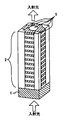
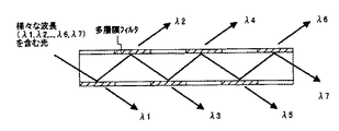
図17は光通信での波長多重通信において多層膜フィルタを使用する場合を説明する概略図である。波長フィルタの応用としては、例えば、光通信での波長多重通信において、波長の分波素子として用いられる。
図17のように多層膜を配置し、波長が多重化された光を次々に多層膜に入射させ、それぞれの多層膜に対応した波長のみが透過または反射されることによって、波長を分波する。
このような多層膜波長フィルタは、1nm以下の波長間隔で多重化されている高密度な波長多重光に対しても、十分な消光比を取りながら分波することが可能である。
しかしながら、このような構成を実現するためには、透過または反射させる波長に対応した、異なる多層膜を、それぞれ独立に形成する必要があり、それぞれの多層膜を入射ビームが反射する面に正確に配置する必要がある。また、それぞれの多層膜に光を入射させるためにはビーム半径を拡大し、さらに異なる多層膜にそれぞれ入射するために十分な光路を取る必要がある。
このようなことから、複数の多層膜を組み合わせる必要があるために一括で形成することができず、実装精度が要求され、さらに、実装できる大きさに対応した素子サイズとなり、数ミクロン角での実装は困難である。
In recent years, light control elements using multilayer films have been used in various optical components. The functions of the light control element include applications such as a wavelength filter, an antireflection film, and a polarization beam splitter.
FIG. 17 is a schematic diagram for explaining a case where a multilayer filter is used in wavelength division multiplexing communication in optical communication. As an application of the wavelength filter, for example, it is used as a wavelength demultiplexing element in wavelength division multiplexing communication in optical communication.
As shown in FIG. 17, a multilayer film is arranged, light with multiplexed wavelengths is successively incident on the multilayer film, and only wavelengths corresponding to the respective multilayer films are transmitted or reflected to demultiplex the wavelengths. .
Such a multilayer film wavelength filter can demultiplex a high-density wavelength-multiplexed light multiplexed at a wavelength interval of 1 nm or less while taking a sufficient extinction ratio.
However, in order to realize such a configuration, it is necessary to independently form different multilayer films corresponding to the wavelengths to be transmitted or reflected, and each multilayer film is accurately formed on the surface where the incident beam is reflected. Need to be placed. In addition, in order to make light incident on each multilayer film, it is necessary to expand the beam radius and to take a sufficient optical path to enter each multilayer film.
For this reason, it is necessary to combine a plurality of multilayer films, and thus it is impossible to form them in a lump, so that mounting accuracy is required, and further, the element size corresponds to the size that can be mounted. Implementation is difficult.
現在の投射光学素子のカラーフィルタは吸収波長が異なる有機材料により構成されているのが一般的である。しかし、透過波長帯域は100nm以上となり、今後、透過波長帯域が50nm以下のLED光源になる場合、カラーフィルタの用途が大きく変わることが予想される。
つまり、高輝度LED光源での色再現性を高めるために、透過波長帯域を10nm以下にすることにより単色性を高めて、色再現性を向上させる必要がある。透過波長帯域の制御は、狭帯域なフィルタを多層膜で構成することが可能である。
しかしながら、異なる波長に対する狭帯域フィルタは、多層膜の層厚または屈折率を精密に制御する必要があるため、画素と同じ大きさで、異なる波長を透過させるカラーフィルタを、多層膜の近接配置で形成することは極めて困難である。さらに、狭帯域なフィルタをすべての光源に独立で形成すると、それぞれの波長に対して多層膜を形成する必要があり、多層膜部品が増えてしまう。
また、多層膜のフィルタは入射角度に対しての透過帯域が異なるという欠点もあり、LEDの発光角度が大きいために入射角度の斜め成分が増えてしまい、透過帯域がシフトするという欠点もあるために、LED光を平行光にする必要があり、光学系が複雑になる。
The color filters of current projection optical elements are generally made of organic materials having different absorption wavelengths. However, the transmission wavelength band is 100 nm or more, and in the future, when the LED light source has a transmission wavelength band of 50 nm or less, the use of the color filter is expected to change significantly.
That is, in order to improve the color reproducibility with a high-luminance LED light source, it is necessary to improve the color reproducibility by increasing the monochromaticity by setting the transmission wavelength band to 10 nm or less. The transmission wavelength band can be controlled by forming a narrow band filter with a multilayer film.
However, narrowband filters for different wavelengths require precise control of the layer thickness or refractive index of the multilayer film, so color filters that transmit the same wavelength and transmit different wavelengths should be placed close to the multilayer film. It is extremely difficult to form. Furthermore, if a narrow band filter is formed independently for all light sources, it is necessary to form a multilayer film for each wavelength, and the number of multilayer film components increases.
In addition, the multilayer filter has the disadvantage that the transmission band is different with respect to the incident angle, and because the emission angle of the LED is large, the oblique component of the incident angle increases, and the transmission band is shifted. In addition, the LED light needs to be parallel light, and the optical system becomes complicated.
DMDによる画像装置では、現在、カラーフィルタが機械駆動され、光源からの光を分光しているが、機械駆動であると、装置自体のサイズが大きくなる。さらに、色変化のスピードにも限界があるために、機械駆動ではない方法でのアクティブなカラーフィルタが期待されかつ幾つかの技術が提案されている(例えば、特許文献1及び2参照)。
多層膜に波長サイズの構造を形成した波長フィルタとしては、特許文献1に開示されているように、台座基板に異なるパターンを予め形成し、その上に自己クローニングによるフォトニック結晶を製作して、波長フィルタにする方法が提案されている。しかしながら、この方法ではパターニングした基板に多層膜を成膜する必要があり、透過波長のシフト量を大きくすることができずに、形成できる波長範囲が限られている。
また、特許文献2に開示されているような方式も提案されている。多層膜に同心円状のパターンを形成することで、レンズ効果と波長フィルタ効果を同時に持たせる構成である。この構造であると、同心円状のパターンでは波長フィルタとして働くが、それ以外の部分へ入射した光はすべて損失となり、光検出器以外のフィルタ機能としては用いることが困難である。
As a wavelength filter in which a structure of wavelength size is formed in a multilayer film, as disclosed in
A method as disclosed in
しかしながら、特許文献1による方法ではパターニングした基板に多層膜を成膜する必要があり、上述したように、透過波長のシフト量を大きくすることができずに、形成できる波長範囲が限られている。
また、特許文献2による構造であると、上述したように、同心円状のパターンでは波長フィルタとして働くが、それ以外の部分へ入射した光はすべて損失となり、光検出器以外のフィルタ機能としては用いることが困難である。さらに、同心円状の構造では有効屈折率の変化割合が場所により、一定量でなくなり、うまく光を入射させる必要がある。
そこで、本発明の目的は、上述した実情を考慮して、多層膜の平面内で領域に分割し、それぞれの領域に異なる空洞率を有する空洞を形成することで、同一面内で異なる波長を透過又は反射させ、微小な領域ごとに異なる波長を分波する光制御素子を提供し、さらにこの光制御素子とレンズ構造と組み合わせることで光利用効率を向上させ、また光路シフト素子と組み合わせることで、ドロップ波長を高速で変化させることができる光学ユニットを提供することにある。
However, in the method according to
Further, as described above, the structure according to
Therefore, in view of the above situation, the object of the present invention is to divide into regions in the plane of the multilayer film, and to form cavities having different cavities in each region, thereby different wavelengths in the same plane. Providing a light control element that transmits or reflects and demultiplexes a different wavelength for each minute region, further improves the light utilization efficiency by combining this light control element and the lens structure, and also combines with a light path shift element. An object of the present invention is to provide an optical unit capable of changing the drop wavelength at high speed.
上記の課題を解決するために、請求項1に記載の発明は、基板と、該基板上に屈折率と層厚の異なる層を交互に積み重ねた多層膜とからなる光制御素子において、前記多層膜に複数の空洞を有する複数の領域を設け、該領域での空洞の空洞率が異なる光制御素子を特徴とする。
また、請求項2に記載の発明は、前記空洞に空気以外の材料が注入される請求項1記載の光制御素子を特徴とする。
また、請求項3に記載の発明は、前記多層膜が、膜厚が1/4波長の光学的厚さの整数倍である屈折率の異なる膜を交互に積み重ねた多層膜である請求項1又は2記載の光制御素子を特徴とする。
また、請求項4に記載の発明は、前記多層膜が、屈折率と膜厚の組み合せが異なる多層膜を、複数組み合わせた多重多層膜である請求項1乃至3のいずれか一項記載の光制御素子を特徴とする。
また、請求項5に記載の発明は、前記多層膜の間に共振器構造を設けた請求項1乃至4のいずれか一項記載の光制御素子を特徴とする。
また、請求項6に記載の発明は、前記複数の空洞が、基板面に平行な面内で構造異方性を有する請求項1乃至5のいずれか一項記載の光制御素子を特徴とする。
また、請求項7に記載の発明は、前記複数の領域に設けられた複数の空洞が、前記領域内で変化する空洞率を有する複数の空洞率である請求項1乃至6のいずれか一項記載の光制御素子を特徴とする。
In order to solve the above problem, the invention according to
The invention according to
According to a third aspect of the present invention, the multilayer film is a multilayer film in which films having different refractive indexes whose film thickness is an integral multiple of an optical thickness of a quarter wavelength are alternately stacked. Or the light control element of 2 is characterized.
The invention according to
According to a fifth aspect of the present invention, there is provided the light control element according to any one of the first to fourth aspects, wherein a resonator structure is provided between the multilayer films.
The invention according to claim 6 is the light control element according to any one of
In the invention according to claim 7, the plurality of cavities provided in the plurality of regions are a plurality of cavities having a cavity ratio that changes in the region. Features the light control element described.
また、請求項8に記載の発明は、請求項1乃至7のいずれか一項記載の、空洞を有する多層膜からなる光制御素子と、異なる波長を発光する発光体と、レンズとを含む光学ユニットにおいて、前記レンズは前記光制御素子と前記発光体との間に設けられる光学ユニットを特徴とする。
また、請求項9に記載の発明は、請求項1乃至7のいずれか一項記載の空洞を有する多層膜からなる光制御素子と、異なる波長を発光する発光体と、光路シフト素子とを含む光学ユニットにおいて、前記光路シフト素子は前記光制御素子と発光体との間に設けられる光学ユニットを特徴とする。
また、請求項10に記載の発明は、前記発光体と前記光路シフト素子の間にレンズを設ける請求項8又は9記載の光学ユニットを特徴とする。
また、請求項11に記載の発明は、前記光制御素子を複数設ける請求項8乃至10のいずれか一項記載の光学ユニットを特徴とする。
また、請求項12に記載の発明は、前記光路シフト素子は、強誘電性液晶から形成されている請求項8乃至11のいずれか一項記載の光学ユニットを特徴とする。
また、請求項13に記載の発明は、前記光路シフト素子は、光学結晶から形成されている請求項8乃至11のいずれか一項記載の光学ユニットを特徴とする。
An invention according to
A ninth aspect of the invention includes a light control element comprising a multilayer film having a cavity according to any one of the first to seventh aspects, a light emitter that emits a different wavelength, and an optical path shift element. In the optical unit, the optical path shift element is an optical unit provided between the light control element and a light emitter.
The invention according to
The invention according to claim 11 is characterized by the optical unit according to any one of
The invention described in
The invention according to
本発明によれば、多層膜を形成し、領域を分割し、その領域に異なる空洞率を有する光の波長サイズの空洞を設けることで、同一の多層膜に対して異なる光学特性を持たせることができ、極めて微小な領域を有する波長フィルタを構成することができる。
さらには、本発明の光学素子(光制御素子)とレンズ、水平(光路)シフト素子を組み合わせることで、高速なアクティブフィルタとなる光学ユニットが形成でき、素子の集積度や安定性を向上させることができる。
According to the present invention, a multilayer film is formed, a region is divided, and cavities having a wavelength size of light having different cavities are provided in the region, so that the same multilayer film has different optical characteristics. Thus, a wavelength filter having a very small area can be configured.
Furthermore, by combining the optical element (light control element) of the present invention, a lens, and a horizontal (optical path) shift element, an optical unit serving as a high-speed active filter can be formed, and the degree of integration and stability of the element can be improved. Can do.
以下、図面を参照して、本発明の実施形態を詳細に説明する。図1は本発明による光制御素子の構造の第1の実施の形態を示す側面図である。図2は図1の構造の上面図である。図3は図2の直線B1−B2での切り口で示す側面図である。
以下で、本発明による光制御素子の第1の実施の形態を図1乃至図3を参照して説明する。図1において、光制御素子PCEは基板1上に屈折率と膜厚の異なる層により多層膜2が形成されている。
図1では屈折率と膜厚が異なる2種類の薄膜3と4を1組として、複数組が積み重なることで、多層膜が形成されている構成を取っているが、多層膜の構成は2種類以上の薄膜構成であっても良い。
例えば、多層膜の構成としては3種類以上の薄膜を1組とした構造であっても良く、また、徐々に屈折率が変化する構造であっても良く、さらに、すべての薄膜構成が異なる構造であっても良い。
Hereinafter, embodiments of the present invention will be described in detail with reference to the drawings. FIG. 1 is a side view showing a first embodiment of the structure of a light control element according to the present invention. FIG. 2 is a top view of the structure of FIG. FIG. 3 is a side view showing the cut along the straight line B1-B2 of FIG.
A first embodiment of a light control element according to the present invention will be described below with reference to FIGS. In FIG. 1, the light control element PCE has a
In FIG. 1, two types of
For example, the structure of the multilayer film may be a structure in which three or more types of thin films are combined, a structure in which the refractive index gradually changes, and a structure in which all the thin film structures are different. It may be.
図2は多層膜2の面からの上面図であり、図1に示すように、領域S1とS2に分かれている。ここでは、2分割された領域のみを示しているが、3分割以上の領域で構成されていても良い。さらに、正方形の領域を仮定しているが、領域は分割されていれば良く、多角形や円形、円筒など不定形の領域であってもよい。
この領域S1、S2には、空洞5が複数形成されている。この空洞5は、図では等間隔な円形構造をしているが、間隔と構造は機能によって変化させても良い。領域S1とS2での空洞が異なる分布で構成されていることが本発明の特徴である。
空洞5に異なる分布を与える方法としては、図のように空洞5の大きさが異なることも1つであるが、他に、空洞同士の間隔や、領域内の単位面積内に分布する空洞の個数などにより異なる分布を与えることができる。
ここで、この空洞5の異なる分布を定量的に表した量を空洞率と定義する。つまり、単位面積あたりに空洞部分の占める割合を空洞率として表す。例えば、空洞5として、半径rの円形形状で周期aとする正方配列で分布していると仮定すると、空洞率はπr2/a2で表すことができる。
また、三角配列であれば、2πr2/√3a2と表すことができる。領域S1、S2ごとに空洞率が異なることが特徴であり、空洞率が異なることで、領域S1、S2に対する多層膜2の光学特性を変化させることができる。
図2では、領域S1、S2に対して円形形状の空洞5が或る周期の正方配列で分布し、円形形状の半径の大きさを変化させることで空洞率を変化させた構成である。このとき、図1は直線A1−A2で基板1と垂直に切断したときの切り口であり、円形形状が存在しない部分を切り取っている。
FIG. 2 is a top view from the surface of the
A plurality of
As a method of giving different distributions to the
Here, the quantity that quantitatively represents the different distribution of the
A triangular arrangement can be expressed as 2πr 2 / √3a 2 . The feature is that the cavities are different for each of the regions S1 and S2, and the optical characteristics of the
In FIG. 2, the
一方、図3は直線B1−B2での切り口であり、円形形状の中心を結んだ直線で切り取っている。空洞部分は、図3に示すように、多層膜2を貫く構造をしている。図では多層膜2の層厚方向に対して平行に形成されているが、層厚方向に対して或る角度を保ちながら斜めに分布していても良い。
空洞率は様々な方法で変化させることが可能であり、製作方法によって柔軟に選択することが可能である。さらに、複数の方法を組み合わせることで、従来では不可能であった緻密な空洞率制御が可能であり、用途に応じて幅広く対応することが可能となる。
ここで、空洞5が波長以下の大きさを有し、一定の周期を有する構造である場合、このような構造はフォトニック結晶配列として知られる構造となる。このフォトニック結晶配列の場合であれば、波長に対する強力な光閉じ込め効果や、異常分散効果を利用することができる。
空洞部分は図1では空気であることを想定しているが、必ずしも空気(屈折率1.0)である必要はない。つまり、空洞部分の屈折率が、多層膜2を構成している材料の屈折率と異なることで、多層膜2を形成している薄膜との屈折率コントラストが生じればよい。従って、空洞部分に空気以外の材料を充填した構造であってもよい。
例えば、波長633nmに対して、多層膜2を屈折率2.2のTiO2と屈折率1.8のSiO2薄膜で形成し、空洞部分に屈折率1.5のポリマ材料を充填した構造でも良い。
また、波長1300nmに対して、多層膜2を屈折率2.3のTiO2と屈折率1.45のSiO2薄膜とし、空洞部分が屈折率3.5のシリコンであっても良い。さらには、波長1300nmに対して、多層膜2を屈折率3.5のシリコンと屈折率1.45のSiO2薄膜とし、空洞部分が屈折率2.2のTiO2であっても良い。
On the other hand, FIG. 3 shows a cut line at a straight line B1-B2, which is cut by a straight line connecting the centers of circular shapes. The hollow portion has a structure that penetrates the
The void ratio can be changed by various methods, and can be selected flexibly according to a manufacturing method. Furthermore, by combining a plurality of methods, it is possible to control the fine void ratio, which has been impossible in the past, and it is possible to respond widely depending on the application.
Here, when the
In FIG. 1, it is assumed that the hollow portion is air, but it is not necessarily air (refractive index 1.0). That is, it is only necessary that the refractive index contrast with the thin film forming the
For example, for a wavelength of 633 nm, the
For the wavelength of 1300 nm, the
このように、空洞部分の屈折率は用途に応じて、様々に選ぶことが可能であり、洞状に形成されている意味で空洞という表記にしている。また、屈折率コントラストが得られるという点では、屈折率が多層膜2を形成している薄膜の1種類と同じ屈折率であっても、本発明の構成を取ることは可能となるので、材料としては2種類以上の屈折率で形成可能となる。
屈折率の異なる媒質を光学的な波長の1/4の整数倍の膜厚で交互に積み重ねると、高い反射率を有する反射鏡(分布ブラッグ反射鏡)を形成できる。この場合、媒質の屈折率の差が大きいほど反射率を大きくすることが可能で、光学素子の多層膜として広く用いられている構造である。
様々な材料に対する成膜方法は広く開発されており、屈折率と膜厚を高精度で制御可能であるため、特定の波長範囲に対して高い反射率が得られる構成を形成できる。本発明においても、分布ブラッグ反射鏡で多層膜2を形成することが可能であり、領域S1、S2を分割して、多層膜2の反射帯域を制御することが可能となる。
As described above, the refractive index of the cavity portion can be variously selected according to the application, and is expressed as a cavity in the sense that it is formed in a sinusoidal shape. In addition, since the refractive index contrast can be obtained, even if the refractive index is the same as that of one of the thin films forming the
When media having different refractive indexes are alternately stacked with a film thickness that is an integral multiple of 1/4 of the optical wavelength, a reflecting mirror (distributed Bragg reflector) having a high reflectance can be formed. In this case, the greater the difference in the refractive index of the medium, the greater the reflectance, and the structure is widely used as a multilayer film of an optical element.
Film formation methods for various materials have been widely developed, and the refractive index and the film thickness can be controlled with high accuracy, so that a structure with high reflectivity can be formed in a specific wavelength range. Also in the present invention, the
以下では、計算結果1として、多層膜2に分布ブラッグ反射鏡を用いて、円形形状で三角配列させた空洞5を形成した時の効果を、波動計算のシミュレーションにより検証した結果を示す。
波動計算シミュレーションには有限差分(FDTD:Finite Difference Time Domain)法を用いた。このシミュレーション方法は、電磁界を表記するマクスウェルの方程式を空間と時間に対して差分化することで、電磁界を直接計算する方法である。
シミュレーションモデルを細かいメッシュで区切って計算するために、メッシュを十分細かくしておけば、任意構造に対してシミュレーションが可能であり、周波数特性などを比較的容易に計算することが可能であり、本実施の形態のような波長程度の大きさで、複雑な形状を有するモデルに対しては、とくに有効である。
In the following, the
A finite difference (FDTD) method was used for the wave calculation simulation. This simulation method is a method of directly calculating an electromagnetic field by differentiating Maxwell's equation expressing the electromagnetic field with respect to space and time.
In order to calculate by dividing the simulation model with fine meshes, if the mesh is sufficiently fine, simulation can be performed for arbitrary structures, and frequency characteristics etc. can be calculated relatively easily. This is particularly effective for a model having a complex shape and a size of about the wavelength as in the embodiment.
図4は計算モデルを示す概略斜視図である。図4の計算モデルは高屈折率媒質と低屈折率媒質を1組として25組を積層した構造であり、円筒構造は基板1上の多層膜2を貫通している。基板1の屈折率は1.45とし、空洞部分の屈折率は1.0とした。
図4では三角格子の周期に対しての単位格子を表記してあり、この単位格子が面内に一様に存在する構造を仮定して、周期境界条件を用いたシミュレーションを行っている。シミュレーションのメッシュサイズとしては20nmとした。
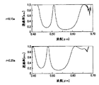
図5は計算例を透過率と波長の関係でそれぞれ示す図である。ここでは、多層膜2(図4)の高屈折率媒質の屈折率を2.0、膜厚を100nmとし、低屈折率媒質の屈折率は1.35、膜厚を120nmとした。図5の(a)〜(h)は円形形状の三角配列空洞が配列されている周期を0.26μmとし、円形形状の半径を変化させている。
空洞5(図4)の半径を徐々に大きくしていくと、図5の(a)から(h)まで変化していく。ここで、図5の(a)でのr=0とは、空洞構造が無いことを意味する。空洞5の半径を大きくすることにより、高反射率を示す波長範囲が短波長側にシフトしていく様子が判る。
例えば、波長750nmの光に対して、異なる半径を有するパターンを異なる領域に形成したときに、パターンが形成されていないr=0では、透過率が1%以下であるのに対して、r=0.30aでは透過率が99%以上となる。
一方、波長600nmに対しては、今度は、r=0.30aであれば、透過率が1%以下であるのに対して、r=0では、透過率が99%以上となる。このように、パターンの形状に対して、透過率の性質が全く逆転する構造を形成することが可能となり、極めて近接した2つの領域に対して、異なる性質の多層膜を形成可能となる。
FIG. 4 is a schematic perspective view showing a calculation model. The calculation model of FIG. 4 has a structure in which 25 pairs of high refractive index medium and low refractive index medium are stacked, and the cylindrical structure penetrates the
In FIG. 4, a unit cell with respect to the period of the triangular lattice is shown, and a simulation using a periodic boundary condition is performed assuming a structure in which the unit cell is uniformly present in the plane. The simulation mesh size was 20 nm.
FIG. 5 is a diagram illustrating calculation examples in terms of the relationship between transmittance and wavelength. Here, the refractive index of the high refractive index medium of the multilayer film 2 (FIG. 4) was 2.0, the film thickness was 100 nm, the refractive index of the low refractive index medium was 1.35, and the film thickness was 120 nm. 5A to 5H, the period in which the circular triangular array cavities are arranged is 0.26 μm, and the radius of the circular shape is changed.
As the radius of the cavity 5 (FIG. 4) is gradually increased, the radius changes from (a) to (h) in FIG. Here, r = 0 in FIG. 5A means that there is no cavity structure. It can be seen that by increasing the radius of the
For example, when a pattern having different radii is formed in different regions with respect to light having a wavelength of 750 nm, the transmittance is 1% or less at r = 0 where the pattern is not formed, whereas r = At 0.30a, the transmittance is 99% or more.
On the other hand, for a wavelength of 600 nm, this time, if r = 0.30a, the transmittance is 1% or less, whereas if r = 0, the transmittance is 99% or more. In this manner, it is possible to form a structure in which the transmittance property is completely reversed with respect to the pattern shape, and it is possible to form a multilayer film having different properties in two very close regions.
従来であれば、このように、場所によって異なる性質を有する反射鏡を形成するためには、膜厚や屈折率が異なる反射鏡を個別に形成する必要があり、一括形成は困難であった。
個別に形成しても、膜厚が異なるために、形成された構造に凹凸が生じてしまい、光の散乱などの原因になる。また、異なる多層膜を精度よく実装するには大きさに限界があり、ディスプレイの画素程度の大きさである10μm程度の大きさを実現するのはさらに困難であった。
そこで、このように多層膜を予め形成した後に、フォトニック結晶配列のような空洞などで形成された微小パターンを形成することによって、反射または透過帯域を変化させることができれば、微小な領域であっても異なる波長に対応した多層膜を形成することが可能である。
さらに、その中心波長の変化は150nmから200nmと幅広く取ることができ、可視光を利用したディスプレイから、光通信用のフィルタまで幅広く適用することができる。
Conventionally, in order to form the reflecting mirrors having different properties depending on the location, it is necessary to individually form the reflecting mirrors having different film thicknesses and refractive indices.
Even if they are formed individually, the film thickness is different, resulting in unevenness in the formed structure, which causes light scattering and the like. Further, there is a limit to the size of mounting different multilayer films with high accuracy, and it has been more difficult to realize a size of about 10 μm, which is about the size of a display pixel.
Thus, if the reflection or transmission band can be changed by forming a micropattern formed by cavities such as a photonic crystal array after forming a multilayer film in advance in this way, it is a very small area. However, it is possible to form multilayer films corresponding to different wavelengths.
Furthermore, the change of the center wavelength can be widely taken from 150 nm to 200 nm, and can be widely applied from a display using visible light to a filter for optical communication.
図6は計算例を透過率と波長の関係でそれぞれ示す図である。図6には、計算結果2として、多層膜構成に対しての変化を示している。多層膜(図4)の高屈折率媒質の屈折率を2.0、膜厚を80nmとし、低屈折率媒質の屈折率は1.35、膜厚を120nmとした。
図6の(a)〜(h)は円形形状の三角配列の空洞が配列されている周期を0.34μmとし、円形形状の半径を変化させた。
図5と同様に半径が変化すると、反射帯域が短波長側にシフトしていく。波長700nmの光に対して、異なる半径を有するパターンを異なる領域に形成した時に、パターンが形成されていないr=0では、透過率が1%以下であるのに対して、r=0.30aでは透過率が99%以上となる。
一方、波長550nmに対しては、今度は、r=0.30aであれば、透過率が1%以下であるのに対して、r=0では、透過率が99%以上となる。このように、膜厚や周期を調整することで、反射帯域を調整することが可能となる。
FIG. 6 is a diagram illustrating calculation examples in terms of the relationship between transmittance and wavelength. FIG. 6 shows a change with respect to the multilayer film configuration as the
In FIGS. 6A to 6H, the period in which the circular triangular array of cavities are arranged is 0.34 μm, and the radius of the circular shape is changed.
When the radius changes as in FIG. 5, the reflection band shifts to the short wavelength side. When patterns having different radii are formed in different regions for light having a wavelength of 700 nm, the transmittance is 1% or less at r = 0 where the pattern is not formed, whereas r = 0.30a. Then, the transmittance is 99% or more.
On the other hand, for a wavelength of 550 nm, this time, when r = 0.30a, the transmittance is 1% or less, whereas when r = 0, the transmittance is 99% or more. Thus, the reflection band can be adjusted by adjusting the film thickness and the period.
図7は本発明による光制御素子の構造の第2の実施の形態を示す図3と同様な側面図である。図7では、光制御素子PCEは、屈折率と膜厚が異なる2種類の薄膜3と4を1組として、複数組が積み重なることで、多層膜6が形成されている。
この多層膜6とは異なる構成を有する多層膜7が多層膜6上に形成され、さらに、多層膜6、7とは異なる構成を有する多層膜8が順次積み重ねられ、多層膜群を形成している。このような構成にすることで、より複雑な反射特性を有する複合多層膜を形成可能となる。
この多層膜群を基板1と平行な面内で複数の領域に分割し、異なる空洞率を有する空洞9、10を形成することで、多層膜群に対しても同一面内において異なる光学特性を有する多層膜が形成可能である。
ここで、空洞9、10は必ずしもすべての多層膜6、7、8に形成している必要はなく、空洞9、10が貫通された多層膜6、7、8と、空洞9、10が形成されていない多層膜6、7、8とが組み合わさった構造であっても良い。
FIG. 7 is a side view similar to FIG. 3 showing a second embodiment of the structure of the light control element according to the present invention. In FIG. 7, in the light control element PCE, a multilayer film 6 is formed by stacking a plurality of sets of two types of
A multilayer film 7 having a configuration different from that of the multilayer film 6 is formed on the multilayer film 6, and a
By dividing the multilayer film group into a plurality of regions in a plane parallel to the
Here, the
図8は本発明による光制御素子の構造の第3の実施の形態を示す図3と同様な側面図である。図8では、光制御素子PCEは、基板1上に、屈折率と膜厚が異なる2種類の薄膜3と4を1組として、複数組が積み重なることで、多層膜6が形成されている。
中央部分に共振器11を設け、多層膜6で挟み込んだ構造である。この構造は多層膜6が共振器11の両面で反射鏡として動作し、ファブリペロー共振器と呼ばれる共振器構造が形成される。
ここでは、共振器部分の光学的な膜厚に対応した波長に対してのみ透過率が高いフィルタが構成できる。共振器11を挟み込む多層膜6は必ずしも同じ構成をしている必要はない。さらに、複数の共振器を複数の多層膜と交互に組み合わせて、複合共振器を形成することも可能である。
このような共振器構造を有する多層膜6を、複数の領域S1、S2に分割し、これらの領域S1、S2に異なる空洞9、10が形成されている。この空洞9、10の空洞率を、領域S1、S2ごとに変化させることにより、共振波長をシフトさせることができる。
図8では空洞9、10を形成している円孔は多層膜6と共振器11を貫通した構造として表記しているが、共振器部分だけ、もしくは多層膜6だけを貫通した構造であっても良い。もちろん、貫通した構造と、貫通しない構造との組み合せでも良い。
FIG. 8 is a side view similar to FIG. 3 showing a third embodiment of the structure of the light control element according to the present invention. In FIG. 8, in the light control element PCE, a multilayer film 6 is formed on a
In this structure, a resonator 11 is provided at the center and sandwiched between multilayer films 6. In this structure, the multilayer film 6 operates as a reflecting mirror on both surfaces of the resonator 11, and a resonator structure called a Fabry-Perot resonator is formed.
Here, a filter having a high transmittance can be configured only for a wavelength corresponding to the optical film thickness of the resonator portion. The multilayer film 6 sandwiching the resonator 11 does not necessarily have the same configuration. Further, a composite resonator can be formed by alternately combining a plurality of resonators with a plurality of multilayer films.
The multilayer film 6 having such a resonator structure is divided into a plurality of regions S1 and S2, and
In FIG. 8, the circular holes forming the
図9は計算例を透過率と波長の関係で異なる半径についてそれぞれ示す図である。図9には共振器構造を導入した時の計算結果を示している。ここでは、多層膜の高屈折率媒質の屈折率を2.08、膜厚を60nmとし、低屈折率媒質の屈折率は1.25、膜厚を100nmとした。
この多層膜の組み合せを6組用意し、中間に屈折率2.08、膜厚120nmの共振器構造を導入した。つまり、3組の多層膜、共振器、3組の多層膜で構成されている。円形形状の三角配列空洞が配列されている周期aを0.26μmとし、円形形状の半径を変化させた。
図9は透過波長のスペクトルを示している。半径が0.15aの時、波長510nmの光はほぼ100%透過するが、半径を0.25aとすると、透過率は10%程度に落ち込む。
一方、半径が0.25aの時、波長480nmの光は、ほぼ100%透過するが、半径を0.15aとすると、透過率は15%程度に落ち込む。このように、空洞の円形形状の半径を変化させるだけで、光学的な性質を変化させることが可能となる。
FIG. 9 is a diagram illustrating calculation examples for different radii depending on the relationship between transmittance and wavelength. FIG. 9 shows a calculation result when the resonator structure is introduced. Here, the refractive index of the high refractive index medium of the multilayer film was 2.08, the film thickness was 60 nm, the refractive index of the low refractive index medium was 1.25, and the film thickness was 100 nm.
Six combinations of the multilayer films were prepared, and a resonator structure having a refractive index of 2.08 and a film thickness of 120 nm was introduced in the middle. That is, it is composed of three sets of multilayer films, a resonator, and three sets of multilayer films. The period a in which the circular triangular array cavities are arranged is 0.26 μm, and the radius of the circular shape is changed.
FIG. 9 shows the spectrum of the transmission wavelength. When the radius is 0.15a, light with a wavelength of 510 nm is transmitted almost 100%, but when the radius is 0.25a, the transmittance drops to about 10%.
On the other hand, when the radius is 0.25a, light with a wavelength of 480 nm is transmitted almost 100%, but when the radius is 0.15a, the transmittance drops to about 15%. As described above, the optical property can be changed only by changing the radius of the circular shape of the cavity.
図10は本発明による光制御素子の構造の第4の実施の形態を示す上面図である。この光制御素子PCEは、基板(図示せず)上に多層膜が形成され、複数の領域S1、S2を設け、異なる領域S1、S2に形成された空洞9、10の形状に異方性を持たせた構造である。領域S1では、形成された空洞9の構造に異方性を設けている。
ここでは、空洞9を楕円形状とし、x方向とy方向の半径が異なる構造を与えてある。また、領域S2では、形成された空洞10は真円形状をしているが、配置されている空洞10の周期は、x方向とy方向に対して異方性を有するようにしてある。
この場合、x方向に平行な直線偏光または円偏光の成分と、y方向に平行な直線偏光または円偏光の成分が受ける特性が異なるなり、偏光による特性分離が可能となる。
例えば、或る波長に対して、偏光分離が可能となることや、同じ偏光成分であっても通過する領域の空洞率が異なることで、波長分離も同時に可能になるなどといった構成も可能となる。このような構成にすることで、光の偏光状態によって多層膜の性質を大きく変化させることが可能となる。
FIG. 10 is a top view showing a fourth embodiment of the structure of the light control element according to the present invention. In this light control element PCE, a multilayer film is formed on a substrate (not shown), a plurality of regions S1, S2 are provided, and the shape of the
Here, the cavity 9 has an elliptical shape and has a structure in which the radii in the x direction and the y direction are different. In the region S2, the formed
In this case, the characteristics received by the linearly polarized light or the circularly polarized light component parallel to the x direction and the linearly polarized light or the circularly polarized light component parallel to the y direction are different, and the characteristics can be separated by the polarized light.
For example, it is possible to configure such that polarization separation is possible for a certain wavelength, and wavelength separation is possible at the same time due to different cavities in the regions through which the same polarization component passes. . With this configuration, the properties of the multilayer film can be greatly changed depending on the polarization state of light.
図11は本発明による光制御素子の構造の第5の実施の形態を示す上面図である。この光制御素子PCEは、基板(図示せず)上に多層膜が形成され、その多層膜に複数の領域S1、S2が設けられている。
図11には、空洞9、10が形成された時の上面図を示している。それぞれの領域S1、S2内では、空洞9、10の面内で異なる形状を形成することで、異方性を持たせてある。
図11では、領域S1、S2を形成し、これらの領域S1、S2が六角形構造をしている。これまでは、正方形を想定していたが、領域S1、S2が多角形であってもよく、用途に応じて様々な形状や大きさを取ることが可能である。
領域S1では空洞9が三角配列で構成され、中心から外側に向けて空洞9の大きさが小さくなる形状をしている。一方、領域S2では、三角配列で構成された空洞10が中心から外側に向けて大きくなる形状をしている。
このように領域S1、S2内で空洞9、10の大きさを変化させることで、等価的な屈折率分布を同時に持たせた多層膜構造も形成可能となり、より複雑な光学特性が得られる多層膜フィルタが形成可能となる。
上記のように、様々な多層膜構成に対して空洞率の異なる空洞を、同一面内に形成することで、異なる性質を有する多層膜を同一平面に形成することが可能となる。
FIG. 11 is a top view showing a fifth embodiment of the structure of the light control element according to the present invention. In the light control element PCE, a multilayer film is formed on a substrate (not shown), and a plurality of regions S1 and S2 are provided in the multilayer film.
FIG. 11 shows a top view when the
In FIG. 11, regions S1 and S2 are formed, and these regions S1 and S2 have a hexagonal structure. Until now, a square was assumed, but the regions S1 and S2 may be polygonal, and can take various shapes and sizes depending on the application.
In the region S1, the cavities 9 are formed in a triangular arrangement, and the size of the cavities 9 decreases from the center toward the outside. On the other hand, in the region S2, the
Thus, by changing the sizes of the
As described above, by forming cavities having different cavities in the same plane for various multilayer film configurations, multilayer films having different properties can be formed on the same plane.
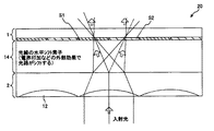
図12は本発明による多層膜を用いた光制御素子を使用する光学ユニットの構成の第1の実施の形態を示す概略図である。図12には、上方に特定の波長帯域だけ透過させることを示す光強度と波長の関係を示す特性図を、かつ下方に光源の透過特性を光強度と波長の関係で示す特性図をともに示している。
図12において、光学ユニット20は、レンズ12上に多層膜6を形成し、多層膜6を領域S1、S2、S3に分割している。それぞれの領域S1、S2、S3には、空洞率が異なる空洞が形成され、多層膜6の性質が異なるようにしてある。光源(図示せず)からの光をレンズ12に対して、異なる角度から入射させ、結像位置をそれぞれの領域S1、S2、S3に分割できる構成で光源を配置する。
多層膜6は様々な性質を持たせるように設計することが可能であるが、例えば、多層膜6に特定の波長に対してのみ高い透過率を有するようなフィルタ機能を持たせる構成とする。
この時、それぞれの領域S1、S2、S3での空洞率を変化させることで、フィルタの波長に対する透過帯域をシフトさせることができ、異なる波長帯域のフィルタを近接配置させることができる。
ここで、入射光源として利用する光の帯域が、フィルタ帯域と一致すれば、その領域では光が透過し、一致しなければその領域では透過しないような光制御素子を構成可能である。
FIG. 12 is a schematic view showing a first embodiment of a configuration of an optical unit using a light control element using a multilayer film according to the present invention. FIG. 12 shows a characteristic diagram showing the relationship between the light intensity and the wavelength indicating that only a specific wavelength band is transmitted upward, and a characteristic diagram showing the transmission characteristic of the light source by the relationship between the light intensity and the wavelength below. ing.
In FIG. 12, the
The multilayer film 6 can be designed to have various properties. For example, the multilayer film 6 is configured to have a filter function having a high transmittance only for a specific wavelength.
At this time, by changing the cavity ratio in each of the regions S1, S2, and S3, the transmission band with respect to the wavelength of the filter can be shifted, and filters of different wavelength bands can be arranged close to each other.
Here, if the band of light used as the incident light source matches the filter band, it is possible to configure a light control element that transmits light in that region and does not transmit in that region unless it matches.
また、光源の波長が広範囲であれば、特定の波長の光だけをそれぞれの領域で切り取ることが可能である。このようなことは、多層膜フィルタだけで可能であるが、レンズ12を用いることで特定の領域に光を集光させることが可能であるので、光利用効率を高めることができる。
さらに、レンズ12の色分散を利用することで、様々な光を有する光を斜めから照射することで、集光位置を変化させることが可能である。従って、集光位置に領域を合わせこむことで、波長分解も可能となる。
集光位置ずれは連続的に起こるので、求められる波長のみを透過させるために、本発明の多層膜フィルタが有効である。また、集光位置ずれは、波長ずれと同じ程度であるために、近接した波長であれば、同一平面内に形成する本発明が効果的である。
また、狭帯域のフィルタを構成することで、透過波長のプロファイルを整形することが可能である。例えば、プロジェクションシステムの照明光としてLEDランプを使用した場合、さらに色再現性を向上させるためには、LEDの中心波長成分からの波長の広がりをカットすることができ、波長成分を抑制することができる。上記では、透過型のフィルタについて記述してあるが、もちろん、反射型のフィルタでも良い。
If the wavelength of the light source is wide, only light of a specific wavelength can be cut out in each region. Such a thing is possible only with the multilayer filter, but since the light can be condensed in a specific region by using the
Furthermore, by using the chromatic dispersion of the
Since the condensing position shift occurs continuously, the multilayer filter of the present invention is effective for transmitting only the required wavelength. Moreover, since the condensing position deviation is about the same as the wavelength deviation, the present invention formed in the same plane is effective if the wavelength is close.
In addition, it is possible to shape the transmission wavelength profile by configuring a narrow band filter. For example, when an LED lamp is used as illumination light for the projection system, the wavelength spread from the central wavelength component of the LED can be cut and the wavelength component can be suppressed in order to further improve color reproducibility. it can. In the above description, the transmission type filter is described. Of course, a reflection type filter may be used.
図13は本発明による多層膜を用いた光制御素子を使用する光学ユニットの構成の第2の実施の形態を示す概略図である。図13の第2の実施の形態では、光学ユニット20は、多層膜6が形成されている基板1と、水平シフト素子を有する基板13との組み合せで構成されている。
基板1の多層膜部分6には、領域S1、S2が形成され、それぞれの領域S1、S2に空洞が形成されており、その空洞率が領域S1、S2ごとに異なっている。
また、基板13には、水平シフト素子14を挟んで、多層膜6とは反対側に光の開口部15を設けてある。水平シフト素子14は、光学結晶や液晶など、光学的な異方性を有する媒質でできており、特定の偏光に対して進む方向が異なる機能を有する。
光は開口部15側から入射し、多層膜6側に抜けていく。水平シフト素子14として一軸性結晶を用いた場合に、無偏光の単色光を入射光として用いた時、光は偏光分離され、水平シフト素子14を伝搬していく。
開口部15の大きさと水平シフト素子14の厚みを調整することにより、分離された偏光をそれぞれの領域S1、S2に入射させることが可能となり、それぞれの偏光に対応した光機能を発現させることができる。
例えば、偏光によって異なる性質が生じてしまう多層膜でも、この構成を取ることにより、偏光依存性を解消させることもできるし、さらに大きな偏光依存性を生じさせることも可能である。
FIG. 13 is a schematic view showing a second embodiment of the configuration of an optical unit using a light control element using a multilayer film according to the present invention. In the second embodiment of FIG. 13, the
In the multilayer film portion 6 of the
The
Light enters from the
By adjusting the size of the
For example, even in a multilayer film in which different properties are generated depending on the polarization, the polarization dependency can be eliminated or even greater polarization dependency can be generated by adopting this configuration.
図14は図13に示した第2の実施の形態の変形例を示す概略図である。この変形例において、光学ユニット20は、また、水平シフト素子14として垂直配置させた強誘電性液晶を用いることが可能である。
この場合、電圧印加により光の進行方向を変化させることが可能となるために、開口部15を図14のように領域の中央に設けることで、入射した光を異なる領域に照射させることも可能となる。
領域ごとの多層膜の光学特性が異なるので、このような構成であると、電圧印加による光学特性の変化を起こすことが可能となり、アクティブな光学素子へ応用が可能である。
このような光の波面の到達場所を変化させる水平シフト素子14は、液晶以外でも光学結晶などで可能であり、同様な性質を有する材料であれば、用途に応じて使い分けることが可能となる。
FIG. 14 is a schematic diagram showing a modification of the second embodiment shown in FIG. In this modification, the
In this case, since it is possible to change the traveling direction of light by applying a voltage, it is possible to irradiate different regions with incident light by providing the
Since the optical characteristics of the multilayer film for each region are different, such a configuration can cause a change in the optical characteristics due to voltage application, and can be applied to an active optical element.
The
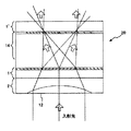
図15は本発明による多層膜を用いた光制御素子を使用する光学ユニットの構成の第3の実施の形態を示す概略図である。図15の光学ユニット20は、レンズ12を有する基板2と、多層膜を有する基板1との間に水平シフト素子14を配置している構成である。
このような構成はそれぞれの素子が別々に分離されていて、光学的な配置が図で示す配置であればよいし、それらの素子が光学的な距離を保ちながら、密着して配置されていても良い。基板1の多層膜部分は領域S1、S2に分割されていて、その分割された領域S1、S2には空洞が形成され、異なる空洞率を有する。
光は基板2側から入射し、集光されながら水平シフト素子14を通過する。この通過時に水平シフト素子14により光の進行方向がシフトし、基板1上の異なる領域S1、S2に集光される。水平シフト素子14は、図13及び図14で述べてきたような領域により異なる光学性能を示す素子として機能する。
ここで、レンズ12を用いることで、光利用効率を高めることができ、図13及び図14では、原理的に50%の損失であったものをさらに高めることができる。
電界印加によるアクティブ素子にすることも可能となり、可変の多層膜フィルタを構成することができる。さらに、図15のように領域の数倍程度の大きさを有するレンズ12をアレイ状に配置し、異なる性質の領域を交互に配置することにより、大きな面積で同一の光学性能を発現させることも可能となる。
FIG. 15 is a schematic view showing a third embodiment of the configuration of an optical unit using a light control element using a multilayer film according to the present invention. The
In such a configuration, each element is separated separately, and the optical arrangement may be the arrangement shown in the figure, and these elements are arranged in close contact while maintaining an optical distance. Also good. The multilayer film portion of the
Light enters from the
Here, the use efficiency of light can be increased by using the
An active element can be formed by applying an electric field, and a variable multilayer filter can be configured. Furthermore, as shown in FIG. 15, the
図16は本発明による多層膜を用いた光制御素子を使用する光学ユニットの構成の第4の実施の形態を示す概略図である。図16の第4の実施の形態において、光学ユニット20は、レンズ12を有する基板2と、多層膜が形成された基板1、1’と、水平シフト素子14から構成される。
ここで、多層膜が形成された基板1、1’は、複数の領域に分割され、それぞれ異なる空洞率となる空洞が形成されている。水平シフト素子14を挟み込むように多層膜が形成された基板1、1’を設けることで、水平シフトする前で光学特性を特定し、水平シフトした後でさらに光学特性を限定するという複数の多層膜構成を取ることができる。
多層膜を形成する材料としては、酸化物として、例えば、SiO2、TiO2、MgO、ZrO2、Ta2O5、ZnO、Nb2O5、Al2O3などがあり、フッ化物として、例えば、AlF3、MgF2、NdF3などがあり、また、その他の化合物としてZnS、CdSなどを用いることができる。
さらに、半導体では、Si、GeなどのIV族半導体、GaAs、AlAs、InP、GaNなどのIII−V族化合物半導体やZnSe、CdTeなどのII−VI族化合物半導体と、と、その混晶であるAlGaAs、GaInAs、GaInAsPなどがある。
金属では、特定の波長に対して、吸収係数が低い場合が存在し、Au、Ag、Al、Cuなどにより形成することが可能である。さらには有機材料で構成することも可能である。
FIG. 16 is a schematic view showing a fourth embodiment of the configuration of an optical unit using a light control element using a multilayer film according to the present invention. In the fourth embodiment shown in FIG. 16, the
Here, the
Examples of the material for forming the multilayer film include oxides such as SiO 2 , TiO 2 , MgO, ZrO 2 , Ta 2 O 5 , ZnO, Nb 2 O 5 , and Al 2 O 3 . For example, there are AlF 3 , MgF 2 , NdF 3 and the like, and ZnS, CdS and the like can be used as other compounds.
Further, the semiconductor is a mixed crystal of a group IV semiconductor such as Si or Ge, a group III-V compound semiconductor such as GaAs, AlAs, InP, or GaN, or a group II-VI compound semiconductor such as ZnSe or CdTe. There are AlGaAs, GaInAs, GaInAsP, and the like.
A metal has a low absorption coefficient for a specific wavelength, and can be formed of Au, Ag, Al, Cu, or the like. Furthermore, it can also be comprised with an organic material.
以下に本発明による光制御素子の製作方法の一例を述べる。透過型か反射型かの用途に対して、基板を選択し、適当な基板を用意する。透過型であれば、用いる光の波長に対して透明であることが必要であり、反射型であればその必要はない。
さらに、この光制御素子と水平シフト素子とを集積化することで、入射光を制御し、異なるフォトニック結晶配列によりアクティブに制御できる波長選択性の高い光制御素子と、その製作方法に関するものである。
例えば、可視光に対して透過型で用いる場合は、ガラス基板や石英基板などを用いることができ、赤外光であれば、半導体基板を用いることが可能である。さらに、基板には透明電極やTFT構成を形成しておいても良く、半導体基板を用いるのであれば、LSIや光デバイスを形成してあっても良い。
この基板に、多層膜を形成する。多層膜の形成には、スパッタ法やCVD法による成膜方法を用いる。基板に直接成膜しても良いし、成膜された多層膜を基板に接合する方法をとっても良い。
この多層膜を形成された基板に、パターニングとエッチングでパターンを形成する。パターニングには、フォトリソグラフィ、電子線リソグラフィ、X線リソグラフィなどのリソグラフィや、ナノインプリントなどの複製パターニングの方法を用いることで可能となる。
空洞の大きさは、光の波長程度であれば、数100nmであるので、上記方法で十分可能である。空洞を形成するには、薬品によるウェットエッチングや、プラズマによるドライエッチングを使用する。
多層膜の厚みは成膜する層数によって変わるが、例えば、1組100nmの薄膜ペアーを20組積層しても2μmであるので、材料を適切に選ぶことで十分にドライエッチングにより貫通させることが可能となる。
An example of a method for manufacturing a light control element according to the present invention will be described below. For a transmissive or reflective application, a substrate is selected and an appropriate substrate is prepared. If it is a transmission type, it is necessary to be transparent with respect to the wavelength of light used, and if it is a reflection type, it is not necessary.
Furthermore, by integrating the light control element and the horizontal shift element, the present invention relates to a light control element with high wavelength selectivity that can control incident light and can be actively controlled by different photonic crystal arrangements, and a manufacturing method thereof. is there.
For example, a glass substrate, a quartz substrate, or the like can be used in the case of using a transmission type with respect to visible light, and a semiconductor substrate can be used in the case of infrared light. Further, a transparent electrode or a TFT structure may be formed on the substrate, and if a semiconductor substrate is used, an LSI or an optical device may be formed.
A multilayer film is formed on this substrate. For the formation of the multilayer film, a film forming method by sputtering or CVD is used. A film may be formed directly on the substrate, or a multilayer film formed may be bonded to the substrate.
A pattern is formed on the substrate on which the multilayer film is formed by patterning and etching. The patterning can be performed by using lithography such as photolithography, electron beam lithography, and X-ray lithography, and replication patterning methods such as nanoimprint.
Since the size of the cavity is several hundreds of nanometers as long as the wavelength of light, the above method is sufficient. In order to form the cavity, chemical wet etching or plasma dry etching is used.
Although the thickness of the multilayer film varies depending on the number of layers to be formed, for example, even if 20 pairs of 100 nm thin films are stacked, it is 2 μm. Therefore, by appropriately selecting the material, it can be sufficiently penetrated by dry etching. It becomes possible.
空洞を形成後、再成膜や有機溶剤塗布とベイク工程により空洞に屈折率媒質を充填することも可能である。パターニングしてから成膜していく方法では、成膜条件に制約が大きくなるのと比較して、このような方法であると、成膜してからパターンを形成するために、設計許容度の高いパターニングが可能となる。
上記では、光学的な性質のみを仮定しているが、これは電磁波全般に対して応用できる性質であり、空洞のサイズと適切な材料の選択により、電波領域での波長に対しても同様な性質を有する。
上述したように、本発明によれば、同一の多層膜構造を有しながら、透過または反射する波長が異なる領域を一括で形成できる光制御素子を提供することができる。
また、本発明によれば、多層膜からなる光制御素子の、透過または反射する波長を制御できる、光利用効率を向上させ、偏光に対する制御や、電圧印加によるアクティブ制御ができる光学ユニットを提供することができる。
After forming the cavity, it is also possible to fill the cavity with a refractive index medium by re-film formation, application of an organic solvent and baking. In the method of forming a film after patterning, the constraint on the film forming conditions becomes larger, and in this method, the design tolerance is increased in order to form a pattern after forming the film. High patterning is possible.
In the above, only optical properties are assumed, but this is a property that can be applied to electromagnetic waves in general, and the same applies to wavelengths in the radio wave region by selecting the size of the cavity and the appropriate material. Has properties.
As described above, according to the present invention, it is possible to provide a light control element capable of collectively forming regions having different wavelengths for transmission or reflection while having the same multilayer film structure.
In addition, according to the present invention, there is provided an optical unit capable of controlling the wavelength of light transmitted or reflected by a light control element composed of a multilayer film, improving the light utilization efficiency, controlling the polarization, and performing active control by applying a voltage. be able to.
1 基板、2 多層膜、3、4 薄膜、5 空洞、6、7、8 多層膜、9、10 空洞、11 共振器構造、12 レンズ、13 基板、14 水平シフト素子、20 光学ユニット、S1 領域、S2 領域、PCE 光制御素子
DESCRIPTION OF
Claims (13)
The optical unit according to claim 8, wherein the optical path shift element is formed of an optical crystal.
Priority Applications (1)
| Application Number | Priority Date | Filing Date | Title |
|---|---|---|---|
| JP2006079746A JP5217100B2 (en) | 2006-03-22 | 2006-03-22 | Optical unit |
Applications Claiming Priority (1)
| Application Number | Priority Date | Filing Date | Title |
|---|---|---|---|
| JP2006079746A JP5217100B2 (en) | 2006-03-22 | 2006-03-22 | Optical unit |
Publications (2)
| Publication Number | Publication Date |
|---|---|
| JP2007256536A true JP2007256536A (en) | 2007-10-04 |
| JP5217100B2 JP5217100B2 (en) | 2013-06-19 |
Family
ID=38630848
Family Applications (1)
| Application Number | Title | Priority Date | Filing Date |
|---|---|---|---|
| JP2006079746A Expired - Fee Related JP5217100B2 (en) | 2006-03-22 | 2006-03-22 | Optical unit |
Country Status (1)
| Country | Link |
|---|---|
| JP (1) | JP5217100B2 (en) |
Cited By (3)
| Publication number | Priority date | Publication date | Assignee | Title |
|---|---|---|---|---|
| EP2042782A1 (en) | 2007-09-28 | 2009-04-01 | Honda Motor Co., Ltd. | Transmission for vehicles |
| CN108490526A (en) * | 2018-04-04 | 2018-09-04 | 长春理工大学 | A kind of reflective spike filter of the poroid micro-structure of multilayer |
| CN108490527A (en) * | 2018-04-04 | 2018-09-04 | 长春理工大学 | A kind of reflective multiband pectination spike filter of the poroid micro-structure of multilayer |
Families Citing this family (1)
| Publication number | Priority date | Publication date | Assignee | Title |
|---|---|---|---|---|
| KR20200034500A (en) | 2018-09-21 | 2020-03-31 | 삼성전자주식회사 | Multi-layer structure and phase shift device using the multi-layer structure |
Citations (10)
| Publication number | Priority date | Publication date | Assignee | Title |
|---|---|---|---|---|
| JPH0882711A (en) * | 1994-09-12 | 1996-03-26 | Nippon Telegr & Teleph Corp <Ntt> | Optical multiplxer and optical demultiplexer |
| JPH11316154A (en) * | 1998-05-01 | 1999-11-16 | Shin Etsu Handotai Co Ltd | Laminating material and optically functional element |
| JP2002162653A (en) * | 2000-11-29 | 2002-06-07 | Minolta Co Ltd | Three-dimensional photonic crystal and method of manufacturing for the same as well as optical element |
| JP2002214579A (en) * | 2001-01-19 | 2002-07-31 | Ricoh Co Ltd | Image display device |
| JP2003121637A (en) * | 2001-10-17 | 2003-04-23 | Nippon Sheet Glass Co Ltd | Fabry-perot filter |
| JP2003273460A (en) * | 2002-03-14 | 2003-09-26 | Japan Science & Technology Corp | Two-dimensional photonic crystal face emitting laser array and two-dimensional photonic crystal face emitting laser |
| JP2003285384A (en) * | 2002-03-27 | 2003-10-07 | Shin Etsu Handotai Co Ltd | Heat ray cutoff and light transmission member |
| JP2004529387A (en) * | 2001-05-02 | 2004-09-24 | カリフォルニア インスティチュート オブ テクノロジー | Photonic crystal microcavity for strong coupling between atoms and hollow field and method of manufacturing the same |
| JP2004354735A (en) * | 2003-05-29 | 2004-12-16 | Daishinku Corp | Light ray cut filter |
| JP2005026567A (en) * | 2003-07-04 | 2005-01-27 | Matsushita Electric Ind Co Ltd | Solid state imaging device and method for manufacturing the same |
-
2006
- 2006-03-22 JP JP2006079746A patent/JP5217100B2/en not_active Expired - Fee Related
Patent Citations (10)
| Publication number | Priority date | Publication date | Assignee | Title |
|---|---|---|---|---|
| JPH0882711A (en) * | 1994-09-12 | 1996-03-26 | Nippon Telegr & Teleph Corp <Ntt> | Optical multiplxer and optical demultiplexer |
| JPH11316154A (en) * | 1998-05-01 | 1999-11-16 | Shin Etsu Handotai Co Ltd | Laminating material and optically functional element |
| JP2002162653A (en) * | 2000-11-29 | 2002-06-07 | Minolta Co Ltd | Three-dimensional photonic crystal and method of manufacturing for the same as well as optical element |
| JP2002214579A (en) * | 2001-01-19 | 2002-07-31 | Ricoh Co Ltd | Image display device |
| JP2004529387A (en) * | 2001-05-02 | 2004-09-24 | カリフォルニア インスティチュート オブ テクノロジー | Photonic crystal microcavity for strong coupling between atoms and hollow field and method of manufacturing the same |
| JP2003121637A (en) * | 2001-10-17 | 2003-04-23 | Nippon Sheet Glass Co Ltd | Fabry-perot filter |
| JP2003273460A (en) * | 2002-03-14 | 2003-09-26 | Japan Science & Technology Corp | Two-dimensional photonic crystal face emitting laser array and two-dimensional photonic crystal face emitting laser |
| JP2003285384A (en) * | 2002-03-27 | 2003-10-07 | Shin Etsu Handotai Co Ltd | Heat ray cutoff and light transmission member |
| JP2004354735A (en) * | 2003-05-29 | 2004-12-16 | Daishinku Corp | Light ray cut filter |
| JP2005026567A (en) * | 2003-07-04 | 2005-01-27 | Matsushita Electric Ind Co Ltd | Solid state imaging device and method for manufacturing the same |
Cited By (4)
| Publication number | Priority date | Publication date | Assignee | Title |
|---|---|---|---|---|
| EP2042782A1 (en) | 2007-09-28 | 2009-04-01 | Honda Motor Co., Ltd. | Transmission for vehicles |
| EP2333382A1 (en) | 2007-09-28 | 2011-06-15 | Honda Motor Co., Ltd. | Transmission for Vehicles |
| CN108490526A (en) * | 2018-04-04 | 2018-09-04 | 长春理工大学 | A kind of reflective spike filter of the poroid micro-structure of multilayer |
| CN108490527A (en) * | 2018-04-04 | 2018-09-04 | 长春理工大学 | A kind of reflective multiband pectination spike filter of the poroid micro-structure of multilayer |
Also Published As
| Publication number | Publication date |
|---|---|
| JP5217100B2 (en) | 2013-06-19 |
Similar Documents
| Publication | Publication Date | Title |
|---|---|---|
| JP7125640B2 (en) | Manufacturing method of transmission type diffraction grating | |
| US9261753B2 (en) | Spectrum filtering for visual displays and imaging having minimal angle dependence | |
| KR101340900B1 (en) | Wire grid polarizer having dual layer structure and method for fabricating the same | |
| Chang-Hasnain | High-contrast gratings as a new platform for integrated optoelectronics | |
| KR20220054386A (en) | Vacuum Bragg grating and manufacturing method thereof | |
| JP4681935B2 (en) | Three-dimensional photonic crystal and optical element using the same | |
| US20010012149A1 (en) | Optical elements comprising photonic crystals and applications thereof | |
| JP2009515203A (en) | Microstructured optical device for polarization and wavelength filter processing | |
| US7009679B2 (en) | Chiral boardband tuning apparatus and method | |
| JP2006047663A (en) | Three-dimensional photonic crystal and optical element using the same | |
| JP2008107720A (en) | Polarizer and its manufacturing method | |
| JP2007148365A (en) | Three-dimensional photonic crystal and functional device including the same | |
| WO2021241701A1 (en) | Optical device and light-emitting device | |
| JP5217100B2 (en) | Optical unit | |
| US7680382B2 (en) | Method for fabricating three-dimensional photonic crystal | |
| JP2004139001A (en) | Optical element, optical modulating element and image display apparatus | |
| JP4427026B2 (en) | Polarizer and polarization separation element | |
| Dems | Monolithic high-contrast gratings: Why do they not scatter light? | |
| JP4689355B2 (en) | Periodic structure and optical element using the periodic structure | |
| CN114930202A (en) | Optical device with phase correction | |
| KR20190006890A (en) | Circular polarization device, notch filter and bandpass filter including the same | |
| JP2001272557A (en) | Optical functional element and its manufacturing method | |
| JP2008276074A (en) | Filter for optical communication, and module for optical communication using the same | |
| Dideban et al. | Photonic crystal channel drop filters based on circular-shaped cavities | |
| JP4975162B2 (en) | Self-cloning photonic crystal for ultraviolet light |
Legal Events
| Date | Code | Title | Description |
|---|---|---|---|
| A621 | Written request for application examination |
Free format text: JAPANESE INTERMEDIATE CODE: A621 Effective date: 20090204 |
|
| RD03 | Notification of appointment of power of attorney |
Free format text: JAPANESE INTERMEDIATE CODE: A7423 Effective date: 20090206 |
|
| A977 | Report on retrieval |
Free format text: JAPANESE INTERMEDIATE CODE: A971007 Effective date: 20110330 |
|
| A131 | Notification of reasons for refusal |
Free format text: JAPANESE INTERMEDIATE CODE: A131 Effective date: 20110712 |
|
| A521 | Written amendment |
Free format text: JAPANESE INTERMEDIATE CODE: A523 Effective date: 20110912 |
|
| A131 | Notification of reasons for refusal |
Free format text: JAPANESE INTERMEDIATE CODE: A131 Effective date: 20120306 |
|
| A521 | Written amendment |
Free format text: JAPANESE INTERMEDIATE CODE: A523 Effective date: 20120501 |
|
| A131 | Notification of reasons for refusal |
Free format text: JAPANESE INTERMEDIATE CODE: A131 Effective date: 20120821 |
|
| A521 | Written amendment |
Free format text: JAPANESE INTERMEDIATE CODE: A523 Effective date: 20121012 |
|
| TRDD | Decision of grant or rejection written | ||
| A01 | Written decision to grant a patent or to grant a registration (utility model) |
Free format text: JAPANESE INTERMEDIATE CODE: A01 Effective date: 20130205 |
|
| A61 | First payment of annual fees (during grant procedure) |
Free format text: JAPANESE INTERMEDIATE CODE: A61 Effective date: 20130218 |
|
| FPAY | Renewal fee payment (event date is renewal date of database) |
Free format text: PAYMENT UNTIL: 20160315 Year of fee payment: 3 |
|
| R151 | Written notification of patent or utility model registration |
Ref document number: 5217100 Country of ref document: JP Free format text: JAPANESE INTERMEDIATE CODE: R151 |
|
| FPAY | Renewal fee payment (event date is renewal date of database) |
Free format text: PAYMENT UNTIL: 20160315 Year of fee payment: 3 |
|
| LAPS | Cancellation because of no payment of annual fees |