JP2007208774A - Phase control circuit - Google Patents
Phase control circuit Download PDFInfo
- Publication number
- JP2007208774A JP2007208774A JP2006026667A JP2006026667A JP2007208774A JP 2007208774 A JP2007208774 A JP 2007208774A JP 2006026667 A JP2006026667 A JP 2006026667A JP 2006026667 A JP2006026667 A JP 2006026667A JP 2007208774 A JP2007208774 A JP 2007208774A
- Authority
- JP
- Japan
- Prior art keywords
- circuit
- flip
- input terminal
- signal
- input
- Prior art date
- Legal status (The legal status is an assumption and is not a legal conclusion. Google has not performed a legal analysis and makes no representation as to the accuracy of the status listed.)
- Pending
Links
- 230000010354 integration Effects 0.000 claims abstract description 21
- 230000003111 delayed effect Effects 0.000 claims abstract description 11
- 239000003990 capacitor Substances 0.000 claims description 18
- 230000032683 aging Effects 0.000 abstract 1
- 230000001934 delay Effects 0.000 abstract 1
- 238000010586 diagram Methods 0.000 description 8
- 230000000630 rising effect Effects 0.000 description 5
- 238000013459 approach Methods 0.000 description 4
- 230000001360 synchronised effect Effects 0.000 description 3
- 230000007423 decrease Effects 0.000 description 2
- 238000001514 detection method Methods 0.000 description 2
- 230000000694 effects Effects 0.000 description 1
- 230000007613 environmental effect Effects 0.000 description 1
- 238000004519 manufacturing process Methods 0.000 description 1
- 238000000034 method Methods 0.000 description 1
Images


Classifications
-
- H—ELECTRICITY
- H03—ELECTRONIC CIRCUITRY
- H03L—AUTOMATIC CONTROL, STARTING, SYNCHRONISATION OR STABILISATION OF GENERATORS OF ELECTRONIC OSCILLATIONS OR PULSES
- H03L7/00—Automatic control of frequency or phase; Synchronisation
- H03L7/06—Automatic control of frequency or phase; Synchronisation using a reference signal applied to a frequency- or phase-locked loop
- H03L7/08—Details of the phase-locked loop
- H03L7/081—Details of the phase-locked loop provided with an additional controlled phase shifter
- H03L7/0812—Details of the phase-locked loop provided with an additional controlled phase shifter and where no voltage or current controlled oscillator is used
-
- H—ELECTRICITY
- H03—ELECTRONIC CIRCUITRY
- H03L—AUTOMATIC CONTROL, STARTING, SYNCHRONISATION OR STABILISATION OF GENERATORS OF ELECTRONIC OSCILLATIONS OR PULSES
- H03L7/00—Automatic control of frequency or phase; Synchronisation
- H03L7/06—Automatic control of frequency or phase; Synchronisation using a reference signal applied to a frequency- or phase-locked loop
- H03L7/08—Details of the phase-locked loop
- H03L7/085—Details of the phase-locked loop concerning mainly the frequency- or phase-detection arrangement including the filtering or amplification of its output signal
- H03L7/091—Details of the phase-locked loop concerning mainly the frequency- or phase-detection arrangement including the filtering or amplification of its output signal the phase or frequency detector using a sampling device
-
- H—ELECTRICITY
- H04—ELECTRIC COMMUNICATION TECHNIQUE
- H04L—TRANSMISSION OF DIGITAL INFORMATION, e.g. TELEGRAPHIC COMMUNICATION
- H04L7/00—Arrangements for synchronising receiver with transmitter
- H04L7/0016—Arrangements for synchronising receiver with transmitter correction of synchronization errors
- H04L7/0033—Correction by delay
- H04L7/0037—Delay of clock signal
-
- H—ELECTRICITY
- H04—ELECTRIC COMMUNICATION TECHNIQUE
- H04L—TRANSMISSION OF DIGITAL INFORMATION, e.g. TELEGRAPHIC COMMUNICATION
- H04L7/00—Arrangements for synchronising receiver with transmitter
- H04L7/02—Speed or phase control by the received code signals, the signals containing no special synchronisation information
- H04L7/033—Speed or phase control by the received code signals, the signals containing no special synchronisation information using the transitions of the received signal to control the phase of the synchronising-signal-generating means, e.g. using a phase-locked loop
Landscapes
- Engineering & Computer Science (AREA)
- Computer Networks & Wireless Communication (AREA)
- Signal Processing (AREA)
- Pulse Circuits (AREA)
- Manipulation Of Pulses (AREA)
- Stabilization Of Oscillater, Synchronisation, Frequency Synthesizers (AREA)
Abstract
Description
本発明は、位相制御回路に関し、特に経時変化や温度変化に拘らず、常に最適なタイミングの調整をすることが可能な位相制御回路に関する。 The present invention relates to a phase control circuit, and more particularly to a phase control circuit capable of always adjusting an optimum timing regardless of a change with time or a change in temperature.
従来の位相制御回路に関連する先行技術文献としては次のようなものがある。 Prior art documents related to the conventional phase control circuit include the following.
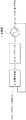
図6はこのような従来の位相制御回路の一例を示す構成ブロック図である。図6において、1は遅延回路、2はフリップフロップ回路である。100はデータ信号、101はクロック信号、101aは遅延回路1により遅延されたクロック信号、102は非反転出力信号、103は反転出力信号である。 FIG. 6 is a block diagram showing an example of such a conventional phase control circuit. In FIG. 6, 1 is a delay circuit and 2 is a flip-flop circuit. 100 is a data signal, 101 is a clock signal, 101a is a clock signal delayed by the delay circuit 1, 102 is a non-inverted output signal, and 103 is an inverted output signal.
データ信号100はフリップフロップ回路2のデータ入力端子に接続され。クロック信号101は遅延回路1の入力端子に接続され、遅延回路1の出力端子はフリップフロップ回路2のクロック入力端子に接続される。フリップフロップ回路2の非反転出力端子からは非反転出力信号102が出力され、フリップフロップ回路2の反転出力端子からは反転出力信号103が出力される。 The data signal 100 is connected to the data input terminal of the flip-flop circuit 2. The clock signal 101 is connected to the input terminal of the delay circuit 1, and the output terminal of the delay circuit 1 is connected to the clock input terminal of the flip-flop circuit 2. A non-inverted output signal 102 is output from the non-inverted output terminal of the flip-flop circuit 2, and an inverted output signal 103 is output from the inverted output terminal of the flip-flop circuit 2.
ここで、図6に示す従来例の動作を説明する。データ信号100はNRZ(Non Return to Zero)とし、フリップフロップ回路2はクロック入力の立ち上がりエッジで動作することとする。 Here, the operation of the conventional example shown in FIG. 6 will be described. The data signal 100 is NRZ (Non Return to Zero), and the flip-flop circuit 2 operates at the rising edge of the clock input.
図6において遅延回路1が無く、クロック信号101がフリップフロップ回路2のクロック入力端子に直接接続されていると仮定する。この場合、例えば、フリップフロップ回路2においてデータ入力端子に入力されるデータ信号100が変化するタイミングとクロック入力端子に入力されるクロック信号101の立ち上がりエッジのタイミングが一致すると出力が不確定になる。 In FIG. 6, it is assumed that there is no delay circuit 1 and the clock signal 101 is directly connected to the clock input terminal of the flip-flop circuit 2. In this case, for example, when the timing at which the data signal 100 input to the data input terminal changes in the flip-flop circuit 2 matches the timing of the rising edge of the clock signal 101 input to the clock input terminal, the output becomes uncertain.
具体的には、クロック信号101の立ち上がりエッジに対するデータ信号100のセットアップ時間、若しくは、ホールド時間を満たさない場合、フリップフロップ回路2の出力は不確定になる。このため、データ信号100とクロック信号101が同期していたとしてもタイミングの調整が必要になる。 Specifically, when the setup time or hold time of the data signal 100 with respect to the rising edge of the clock signal 101 is not satisfied, the output of the flip-flop circuit 2 becomes uncertain. Therefore, even if the data signal 100 and the clock signal 101 are synchronized, timing adjustment is required.
データ信号100、若しくは、クロック信号101のどちらかに遅延回路を使用すればタイミングを調整することができる。ただし、クロック信号の帯域に比べてデータ信号の方の帯域が広い場合が多いので、一般にクロック信号の方に遅延回路を使用する。図6はクロック信号101に遅延回路1を使用した場合を示している。 If a delay circuit is used for either the data signal 100 or the clock signal 101, the timing can be adjusted. However, since the data signal band is often wider than the clock signal band, a delay circuit is generally used for the clock signal. FIG. 6 shows a case where the delay circuit 1 is used for the clock signal 101.
この結果、フリップフロップ回路2のクロック入力端子に入力されるクロック信号101に遅延回路1を入れることにより、フリップフロップ回路2のデータ入力端子に入力されるデータ信号100の変化のタイミングとクロック入力端子に入力されるクロック信号101aの立ち上がりエッジのタイミングが最適化されるので、安定した出力信号を出力することが可能になる。 As a result, when the delay circuit 1 is inserted into the clock signal 101 input to the clock input terminal of the flip-flop circuit 2, the change timing of the data signal 100 input to the data input terminal of the flip-flop circuit 2 and the clock input terminal Since the timing of the rising edge of the clock signal 101a input to is optimized, a stable output signal can be output.
図7はこのような従来の位相制御回路の他の一例を示す構成ブロック図である。図7において、3は位相検出器、4はループフィルタ、5は発振器、104はリファレンス信号、105は出力信号である。 FIG. 7 is a configuration block diagram showing another example of such a conventional phase control circuit. In FIG. 7, 3 is a phase detector, 4 is a loop filter, 5 is an oscillator, 104 is a reference signal, and 105 is an output signal.
位相検出器3の一方の入力端子にはリファレンス信号が入力され、位相検出器3の出力端子はループフィルタ4の入力端子に接続される。ループフィルタ4の出力端子は発振器5の入力端子に接続され、発振器5の出力端子からは出力信号105が出力されると共に位相検出器3の他方の入力端子に接続される。 A reference signal is input to one input terminal of the phase detector 3, and an output terminal of the phase detector 3 is connected to an input terminal of the loop filter 4. The output terminal of the loop filter 4 is connected to the input terminal of the oscillator 5, and the output signal 105 is output from the output terminal of the oscillator 5 and is connected to the other input terminal of the phase detector 3.
ここで、図7に示す従来例の動作を説明する。図7に示す回路は、一般にPLL(Phase Locked Loop)と呼ばれ、リファレンス信号104に正確に同期した周波数の信号を出力信号105として出力する。 Here, the operation of the conventional example shown in FIG. 7 will be described. The circuit shown in FIG. 7 is generally called a PLL (Phase Locked Loop), and outputs a signal having a frequency accurately synchronized with the reference signal 104 as the output signal 105.
具体的には、外部から入力されるリファレンス信号104と発振器5の出力である出力信号105の位相差を位相検出器3で検出し、検出結果をループフィルタ4において発振器5の制御電圧に変換して位相差が一定になるように自動制御する。 Specifically, the phase difference between the reference signal 104 input from the outside and the output signal 105 output from the oscillator 5 is detected by the phase detector 3, and the detection result is converted into the control voltage of the oscillator 5 by the loop filter 4. Automatically control the phase difference to be constant.
この結果、リファレンス信号104と発振器5の出力信号105の位相差を位相検出器3で検出し、検出結果をループフィルタ4において発振器5の制御電圧に変換して位相差が一定になるように自動制御することにより、リファレンス信号104に正確に同期した周波数の信号を出力信号105として出力することが可能になる。 As a result, the phase difference between the reference signal 104 and the output signal 105 of the oscillator 5 is detected by the phase detector 3, and the detection result is converted into the control voltage of the oscillator 5 by the loop filter 4 so that the phase difference becomes constant. By controlling, it becomes possible to output a signal having a frequency accurately synchronized with the reference signal 104 as the output signal 105.
しかし、図6に示す従来例では、製造出荷時等の特定の時点の周囲環境条件でデータ信号100とクロック信号101のタイミングが調整できたとしても、データ信号100の経路とクロック信号101の経路が異なることや遅延回路1自体の特性により、使用温度環境の変化や経時変化からタイミングが次第に合わなくなってくるという問題点があった。 However, in the conventional example shown in FIG. 6, even if the timing of the data signal 100 and the clock signal 101 can be adjusted under ambient environmental conditions at a specific time such as at the time of manufacture and shipment, the path of the data signal 100 and the path of the clock signal 101 There is a problem in that the timing gradually becomes inconsistent due to changes in the operating temperature environment and changes over time due to differences in the delay time and the characteristics of the delay circuit 1 itself.
また、図7に示す従来例では、リファレンス信号104と発振器5の出力信号105の位相差を一定になるように制御はできるものの、このPLLの技術を流用してフリップフロップ回路におけるデータ信号とクロック信号のタイミングを合わせる簡単な回路構成は無かった。 In the conventional example shown in FIG. 7, although the phase difference between the reference signal 104 and the output signal 105 of the oscillator 5 can be controlled to be constant, the data signal and clock in the flip-flop circuit are diverted using this PLL technique. There was no simple circuit configuration to match the signal timing.
従って本発明が解決しようとする課題は、経時変化や温度変化に拘らず、常に最適なタイミングの調整をすることが可能な位相制御回路を実現することにある。 Therefore, the problem to be solved by the present invention is to realize a phase control circuit capable of always adjusting the optimum timing regardless of changes with time or temperature.
このような課題を達成するために、本発明のうち請求項1記載の発明は、
位相を制御する位相制御回路において、
クロック信号を遅延する可変遅延回路と、前記遅延されたクロック信号がクロック入力端子に入力され、データ信号がデータ入力端子に入力される第1のフリップフロップ回路と、前記データ信号がクロック入力端子に入力され、前記遅延されたクロック信号がデータ入力端子に入力される第2のフリップフロップ回路と、この第2のフリップフロップ回路の出力信号に基づいて前記可変遅延回路の遅延量を制御する積分回路とを備えたことにより、経時変化や温度変化に拘らず、常に最適なタイミングの調整をすることが可能になる。
In order to achieve such a problem, the invention according to claim 1 of the present invention is:
In the phase control circuit that controls the phase,
A variable delay circuit for delaying a clock signal; a first flip-flop circuit in which the delayed clock signal is input to a clock input terminal; and a data signal is input to the data input terminal; and the data signal is input to the clock input terminal. A second flip-flop circuit that receives the delayed clock signal input to the data input terminal, and an integration circuit that controls the delay amount of the variable delay circuit based on the output signal of the second flip-flop circuit Thus, it is possible to always adjust the optimum timing regardless of changes with time or temperature.
請求項2記載の発明は、
請求項1記載の発明である位相制御回路において、
前記可変遅延回路が、
前記積分回路の出力に応じて遅延量を変化させることにより、経時変化や温度変化に拘らず、常に最適なタイミングの調整をすることが可能になる。
The invention according to claim 2
In the phase control circuit according to claim 1,
The variable delay circuit is
By changing the delay amount in accordance with the output of the integration circuit, it is possible to always adjust the optimum timing regardless of changes over time or temperature changes.
請求項3記載の発明は、
請求項1若しくは請求項2記載の発明である位相制御回路において、
前記積分回路が、
一端が前記第2のフリップフロップ回路の非反転出力端子に接続される第1の抵抗と、一端が前記第1の抵抗の他端に接続される第1のコンデンサと、一端が前記第2のフリップフロップ回路の反転出力端子に接続される第2の抵抗と、一端が前記第2の抵抗の他端に接続され、他端が接地される第2のコンデンサと、反転入力端子が前記第1の抵抗の他端及び前記第1のコンデンサの一端にそれぞれ接続され、非反転入力端子が前記第2の抵抗の他端及び前記第2のコンデンサの一端にそれぞれ接続され、出力端子が前記第1のコンデンサの他端に接続される増幅器とから構成されることにより、経時変化や温度変化に拘らず、常に最適なタイミングの調整をすることが可能になる。
The invention described in claim 3
In the phase control circuit according to claim 1 or claim 2,
The integrating circuit is
A first resistor having one end connected to the non-inverting output terminal of the second flip-flop circuit, a first capacitor having one end connected to the other end of the first resistor, and one end being the second resistor A second resistor connected to the inverting output terminal of the flip-flop circuit, a second capacitor having one end connected to the other end of the second resistor and the other end grounded, and an inverting input terminal connected to the first resistor The other end of the first resistor and one end of the first capacitor, the non-inverting input terminal is connected to the other end of the second resistor and the one end of the second capacitor, respectively, and the output terminal is the first terminal. The amplifier is connected to the other end of the capacitor, so that the optimum timing can always be adjusted regardless of changes with time and temperature.
請求項4記載の発明は、
位相を制御する位相制御回路において、
クロック信号を遅延する可変遅延回路と、前記遅延されたクロック信号がクロック入力端子に入力され、データ信号がデータ入力端子に入力される第1のフリップフロップ回路と、前記データ信号がクロック入力端子に入力され、前記遅延されたクロック信号がデータ入力端子に入力される第2のフリップフロップ回路と、この第2のフリップフロップ回路の出力信号に基づいて前記可変遅延回路の遅延量を機械的な駆動力により制御する積分回路とを備えたことにより、経時変化や温度変化に拘らず、常に最適なタイミングの調整をすることが可能になる。
The invention according to claim 4
In the phase control circuit that controls the phase,
A variable delay circuit for delaying a clock signal; a first flip-flop circuit in which the delayed clock signal is input to a clock input terminal; and a data signal is input to the data input terminal; and the data signal is input to the clock input terminal. A second flip-flop circuit that receives the delayed clock signal input to the data input terminal, and mechanically drives the delay amount of the variable delay circuit based on the output signal of the second flip-flop circuit By providing the integration circuit controlled by force, it becomes possible to always adjust the optimum timing regardless of changes with time and temperature.
請求項5記載の発明は、
請求項4記載の発明である位相制御回路において、
前記可変遅延回路が、
前記積分回路からの機械的駆動力に応じて遅延量を変化させることにより、経時変化や温度変化に拘らず、常に最適なタイミングの調整をすることが可能になる。
The invention according to claim 5
In the phase control circuit according to claim 4,
The variable delay circuit is
By changing the delay amount in accordance with the mechanical driving force from the integration circuit, it is possible to always adjust the optimum timing regardless of changes over time and temperature changes.
請求項6記載の発明は、
請求項4若しくは請求項5記載の発明である位相制御回路において、
前記積分回路が、
モータと、前記第2のフリップフロップ回路の出力信号の論理レベルに応じて前記モータの回転方向を制御して駆動するモータ駆動回路とから構成されることにより、経時変化や温度変化に拘らず、常に最適なタイミングの調整をすることが可能になる。
The invention described in claim 6
In the phase control circuit according to claim 4 or claim 5,
The integrating circuit is
By comprising a motor and a motor drive circuit that drives by controlling the rotation direction of the motor according to the logic level of the output signal of the second flip-flop circuit, regardless of changes over time or temperature, It becomes possible to always adjust the optimum timing.
本発明によれば次のような効果がある。
請求項1,2及び請求項3の発明によれば、データ信号がクロック入力端子に入力され、クロック信号がデータ入力端子に入力された第2のフリップフロップ回路の出力を積分回路により積分し、この積分された出力に基づいて可変遅延回路を制御することにより、クロック信号のタイミングが最適化されるので、経時変化や温度変化に拘らず、常に最適なタイミングの調整をすることが可能な位相制御回路の実現が可能になる。
The present invention has the following effects.
According to the first, second and third aspects of the invention, the data signal is input to the clock input terminal, the output of the second flip-flop circuit in which the clock signal is input to the data input terminal is integrated by the integrating circuit, By controlling the variable delay circuit based on this integrated output, the timing of the clock signal is optimized, so that it is possible to always adjust the optimal timing regardless of changes over time and temperature. A control circuit can be realized.
請求項4,5及び請求項6の発明によれば、データ信号がクロック入力端子に入力され、クロック信号がデータ入力端子に入力された第2のフリップフロップ回路の出力を積分回路により機械的な駆動力に変換し、この駆動力に基づいて可変遅延回路を制御することにより、クロック信号のタイミングが最適化されるので、経時変化や温度変化に拘らず、常に最適なタイミングの調整をすることが可能の実現が可能になる。 According to the inventions of claims 4, 5 and 6, the output of the second flip-flop circuit in which the data signal is input to the clock input terminal and the clock signal is input to the data input terminal is mechanically processed by the integrating circuit. By converting to driving force and controlling the variable delay circuit based on this driving force, the timing of the clock signal is optimized, so the optimum timing is always adjusted regardless of changes over time and temperature changes. Can be realized.
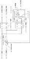
以下本発明を図面を用いて詳細に説明する。図1は本発明に係る位相制御回路の一実施例を示す構成ブロック図である。図1において100,101,101a,102及び103は図6と同一符号を付してあり、6は可変遅延回路、7はフリップフロップ回路、8及び9は抵抗、10及び11はコンデンサ、12は増幅器である。 Hereinafter, the present invention will be described in detail with reference to the drawings. FIG. 1 is a block diagram showing the configuration of an embodiment of a phase control circuit according to the present invention. In FIG. 1, reference numerals 100, 101, 101a, 102 and 103 are assigned the same reference numerals as in FIG. 6, 6 is a variable delay circuit, 7 is a flip-flop circuit, 8 and 9 are resistors, 10 and 11 are capacitors, 12 is It is an amplifier.
また、抵抗8、抵抗9、コンデンサ10、コンデンサ11及び増幅器12は積分回路50を構成している。 In addition, the resistor 8, the resistor 9, the capacitor 10, the capacitor 11, and the amplifier 12 constitute an integrating circuit 50.
データ信号100はフリップフロップ回路2のデータ入力端子及びフリップフロップ回路7のクロック入力端子にそれぞれ接続される。クロック信号101は可変遅延回路6の入力端子に接続され、可変遅延回路6の出力端子はフリップフロップ回路2のクロック入力端子及びフリップフロップ回路7のデータ入力端子にそれぞれ接続される。 The data signal 100 is connected to the data input terminal of the flip-flop circuit 2 and the clock input terminal of the flip-flop circuit 7, respectively. The clock signal 101 is connected to the input terminal of the variable delay circuit 6, and the output terminal of the variable delay circuit 6 is connected to the clock input terminal of the flip-flop circuit 2 and the data input terminal of the flip-flop circuit 7, respectively.
フリップフロップ回路7の非反転出力端子は抵抗8の一端に接続され、抵抗8の他端はコンデンサ10の一端及び増幅器12の反転入力端子にそれぞれ接続される。フリップフロップ回路7の反転出力端子は抵抗9の一端に接続され、抵抗9の他端はコンデンサ11の一端及び増幅器12の非反転入力端子にそれぞれ接続される。 The non-inverting output terminal of the flip-flop circuit 7 is connected to one end of the resistor 8, and the other end of the resistor 8 is connected to one end of the capacitor 10 and the inverting input terminal of the amplifier 12. The inverting output terminal of the flip-flop circuit 7 is connected to one end of the resistor 9, and the other end of the resistor 9 is connected to one end of the capacitor 11 and the non-inverting input terminal of the amplifier 12.
コンデンサ11の他端は接地され、増幅器12の出力端子は可変遅延回路6の制御端子及びコンデンサ10の他端にそれぞれ接続される。フリップフロップ回路2の非反転出力端子からは非反転出力信号102が出力され、反転出力端子からは反転出力信号103が出力される。 The other end of the capacitor 11 is grounded, and the output terminal of the amplifier 12 is connected to the control terminal of the variable delay circuit 6 and the other end of the capacitor 10, respectively. A non-inverted output signal 102 is output from the non-inverted output terminal of the flip-flop circuit 2, and an inverted output signal 103 is output from the inverted output terminal.
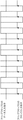
ここで、図1に示す実施例の動作を図2、図3及び図4を用いて説明する。図2はフリップフロップ回路2の動作タイミングを示すタイミングチャート、図3及び図4はフリップフロップ回路2及びフリップフロップ回路7の動作タイミングを示すタイミングチャートである。 Here, the operation of the embodiment shown in FIG. 1 will be described with reference to FIGS. FIG. 2 is a timing chart showing the operation timing of the flip-flop circuit 2, and FIGS. 3 and 4 are timing charts showing the operation timing of the flip-flop circuit 2 and the flip-flop circuit 7.
基本的な動作は図6の従来例とほぼ同一であり、異なる点はフリップフロップ回路7及び積分回路50を追加したことである。図2はフリップフロップ回路2のデータ入力とクロック入力のタイミングが最適の場合のタイミングチャートを示している。すなわち、データ信号100の変化時ではなく、安定している時にクロック信号101aの立ち上がりエッジのタイミングが来ている。 The basic operation is almost the same as that of the conventional example of FIG. 6, and the difference is that a flip-flop circuit 7 and an integration circuit 50 are added. FIG. 2 shows a timing chart when the timing of data input and clock input of the flip-flop circuit 2 is optimum. That is, the timing of the rising edge of the clock signal 101a comes not when the data signal 100 changes but when it is stable.
図3はフリップフロップ回路2のデータ入力のタイミングが最適なタイミングより早い場合のタイミングチャートを示している。図3に示すように、フリップフロップ回路7の非反転出力信号は最初の不定期間を除いて常にローレベルとなり、反転出力信号は最初の不定期間を除いて常にハイレベルとなる。 FIG. 3 shows a timing chart when the data input timing of the flip-flop circuit 2 is earlier than the optimum timing. As shown in FIG. 3, the non-inverted output signal of the flip-flop circuit 7 is always at a low level except for the first indefinite period, and the inverted output signal is always at a high level except for the first indefinite period.
そして、このフリップフロップ回路7の非反転出力信号及び反転出力信号が積分回路50に入力されると、積分回路50の出力信号は徐々に大きくなる。 When the non-inverted output signal and the inverted output signal of the flip-flop circuit 7 are input to the integrating circuit 50, the output signal of the integrating circuit 50 gradually increases.
ここで、可変遅延回路6の特性が制御端子に入力される制御信号の大きさに応じて遅延量が変化すると仮定する。すなわち、制御信号が大きい場合は遅延量が大きくなり、制御信号が小さい場合は遅延量が小さくなる。 Here, it is assumed that the delay amount of the variable delay circuit 6 changes according to the magnitude of the control signal input to the control terminal. That is, when the control signal is large, the delay amount is large, and when the control signal is small, the delay amount is small.
積分回路50の出力信号が徐々に大きくなると、それに応じて可変遅延回路6の遅延量が徐々に大きくなり、最適なタイミングより早く入力されていたクロック信号101aは最適なタイミングに近づくことになる。 When the output signal of the integrating circuit 50 gradually increases, the delay amount of the variable delay circuit 6 gradually increases accordingly, and the clock signal 101a input earlier than the optimal timing approaches the optimal timing.
また、図6はフリップフロップ回路2のデータ入力のタイミングが最適なタイミングより遅い場合のタイミングチャートを示している。図6に示すように、フリップフロップ回路7の非反転出力信号は最初の不定期間を除いて常にハイレベルとなり、反転出力信号は最初の不定期間を除いて常にローレベルとなる。 FIG. 6 shows a timing chart when the data input timing of the flip-flop circuit 2 is later than the optimum timing. As shown in FIG. 6, the non-inverted output signal of the flip-flop circuit 7 is always at high level except for the first indefinite period, and the inverted output signal is always at low level except for the first indefinite period.
そして、このフリップフロップ回路7の非反転出力信号及び反転出力信号が積分回路50に入力されると、積分回路50の出力信号は徐々に小さくなる。 When the non-inverted output signal and the inverted output signal of the flip-flop circuit 7 are input to the integrating circuit 50, the output signal of the integrating circuit 50 gradually decreases.
積分回路50の出力信号が徐々に小さくなると、それに応じて可変遅延回路6の遅延量が徐々に小さくなり、最適なタイミングより遅く入力されていたクロック信号101aは最適なタイミングに近づくことになる。 When the output signal of the integrating circuit 50 is gradually reduced, the delay amount of the variable delay circuit 6 is gradually reduced accordingly, and the clock signal 101a input later than the optimum timing approaches the optimum timing.
この結果、データ信号100がクロック入力端子に入力され、クロック信号101aがデータ入力端子に入力されたフリップフロップ回路7の出力を積分回路50により積分し、この積分された出力に基づいて可変遅延回路6を制御することにより、クロック信号101のタイミングが最適化されるので、経時変化や温度変化に拘らず、常に最適なタイミングの調整をすることが可能になる。 As a result, the output of the flip-flop circuit 7 in which the data signal 100 is input to the clock input terminal and the clock signal 101a is input to the data input terminal is integrated by the integration circuit 50, and the variable delay circuit is based on the integrated output. 6 is optimized, the timing of the clock signal 101 is optimized, so that the optimum timing can always be adjusted regardless of changes over time or temperature.
なお、図1に示す実施例においては積分回路50を差動入力構成としているが、必ずしも差動入力構成とする必要は無く、シングル入力で構成してもよい。 In the embodiment shown in FIG. 1, the integration circuit 50 has a differential input configuration. However, the integration circuit 50 is not necessarily required to have a differential input configuration, and may be configured with a single input.
また、図1に示す実施例においては積分回路50が電気部品で構成されているが、必ずしもそうする必要は無く、モータ等の機械部品を用いて機械的に積分を行ってもよい。 Further, in the embodiment shown in FIG. 1, the integration circuit 50 is constituted by electric parts, but it is not always necessary to do so, and mechanical integration may be performed using a machine part such as a motor.
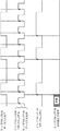
この場合の動作を図5を用いて説明する。図5は本発明に係る位相制御回路の他の実施例を示す構成ブロック図である。図5において2,7,100,101,101a,102,103は図1と同一符号を付してあり、6aは可変遅延回路、13はモータ駆動回路、14はモータである。また、モータ駆動回路13及びモータ14は積分回路51を構成している。
The operation in this case will be described with reference to FIG. FIG. 5 is a block diagram showing the configuration of another embodiment of the phase control circuit according to the present invention. 5, reference numerals 2, 7, 100, 101, 101a, 102, and 103 are assigned the same reference numerals as in FIG. 1, 6a is a variable delay circuit, 13 is a motor drive circuit, and 14 is a motor. The
フリップフロップ回路7の非反転出力端子はモータ駆動回路13の一方の入力端子に接続され、フリップフロップ回路7の反転出力端子はモータ駆動回路13の他方の入力端子に接続される。モータ駆動回路13の一方の出力端子はモータ14の一方の入力端子に接続され、モータ駆動回路13の他方の出力端子はモータ14の他方の入力端子に接続される。
The non-inverting output terminal of the flip-flop circuit 7 is connected to one input terminal of the
また、モータ14の回転部分が可変遅延回路6aの遅延制御用ロータリースイッチに接続される。その他の接続に関しては図1と同じため、説明を省略する。 The rotating portion of the motor 14 is connected to the delay control rotary switch of the variable delay circuit 6a. The other connections are the same as in FIG.
基本的な動作は図1の実施例とほぼ同一であり、異なる点は積分回路51がモータ駆動回路13及びモータ14で構成され、可変遅延回路6aが機械的駆動力により制御されるようになった点である。
The basic operation is almost the same as that of the embodiment of FIG. 1, and the difference is that the integration circuit 51 is composed of the
図1に示す実施例と同様に、フリップフロップ回路2のデータ入力のタイミングが最適なタイミングより早い場合、フリップフロップ回路7の非反転出力信号は最初の不定期間を除いて常にローレベルとなり、反転出力信号は最初の不定期間を除いて常にハイレベルとなる。 As in the embodiment shown in FIG. 1, when the data input timing of the flip-flop circuit 2 is earlier than the optimum timing, the non-inverted output signal of the flip-flop circuit 7 is always at a low level except for the first indefinite period and is inverted. The output signal is always high except for the first indefinite period.
フリップフロップ回路7の非反転出力がローレベルで、反転出力がハイレベルの間、モータ駆動回路13はモータ14を一定速度で一方向に回転させる。これにより可変遅延回路6aの遅延制御用ロータリースイッチが回され、遅延量が徐々に大きくなり、最適なタイミングより早く入力されていたクロック信号101aは最適なタイミングに近づくことになる。
While the non-inverted output of the flip-flop circuit 7 is at a low level and the inverted output is at a high level, the
同様に、フリップフロップ回路2のデータ入力のタイミングが最適なタイミングより遅い場合、フリップフロップ回路7の非反転出力信号は最初の不定期間を除いて常にハイレベルとなり、反転出力信号は最初の不定期間を除いて常にローレベルとなる。 Similarly, when the data input timing of the flip-flop circuit 2 is later than the optimum timing, the non-inverted output signal of the flip-flop circuit 7 is always at a high level except for the first indefinite period, and the inverted output signal is in the first indefinite period. Always low except for.
フリップフロップ回路7の非反転出力がハイレベルで、反転出力がローレベルの間、モータ駆動回路13はモータ14を一定速度で逆方向に回転させる。これにより可変遅延回路6aの遅延制御用ロータリースイッチが回され、遅延量が徐々に小さくなり、最適なタイミングより遅く入力されていたクロック信号101aは最適なタイミングに近づくことになる。
While the non-inverted output of the flip-flop circuit 7 is at the high level and the inverted output is at the low level, the
この結果、データ信号100がクロック入力端子に入力され、クロック信号101aがデータ入力端子に入力されたフリップフロップ回路7の出力を積分回路51により機械的な回転動作に変換し、この回転に基づいて可変遅延回路6aを制御することにより、クロック信号101のタイミングが最適化されるので、経時変化や温度変化に拘らず、常に最適なタイミングの調整をすることが可能になる。 As a result, the data signal 100 is input to the clock input terminal, and the output of the flip-flop circuit 7 having the clock signal 101a input to the data input terminal is converted into a mechanical rotation operation by the integration circuit 51. Based on this rotation, By controlling the variable delay circuit 6a, the timing of the clock signal 101 is optimized, so that the optimum timing can always be adjusted regardless of changes over time and temperature.
また、図5に示す実施例においては積分回路51からの回転動作により可変遅延回路6aを制御していたが、必ずしも回転動作である必要は無く、機械的な駆動力により可変遅延回路6aを制御すればよい。 In the embodiment shown in FIG. 5, the variable delay circuit 6a is controlled by the rotation operation from the integration circuit 51. However, the variable delay circuit 6a is not necessarily a rotation operation, and the variable delay circuit 6a is controlled by a mechanical driving force. do it.
例えば、積分回路51からの回転動作を左右にスライドする動作に変換し、可変遅延回路6aをスライドスイッチにより遅延量を切り替えるものにしてもよい。 For example, the rotation operation from the integration circuit 51 may be converted into a left / right sliding operation, and the variable delay circuit 6a may be switched by a slide switch.
1 遅延回路
2,7 フリップフロップ回路
3 位相検出器
4 ループフィルタ
5 発振器
6,6a 可変遅延回路
8,9 抵抗
10,11 コンデンサ
12 増幅器
13 モータ駆動回路
14 モータ
50,51 積分回路
100 データ信号
101,101a クロック信号
102 非反転出力信号
103 反転出力信号
104 リファレンス信号
105 出力信号
DESCRIPTION OF SYMBOLS 1 Delay circuit 2, 7 Flip-flop circuit 3 Phase detector 4 Loop filter 5 Oscillator 6, 6a Variable delay circuit 8, 9 Resistance 10, 11 Capacitor 12
Claims (6)
クロック信号を遅延する可変遅延回路と、
前記遅延されたクロック信号がクロック入力端子に入力され、データ信号がデータ入力端子に入力される第1のフリップフロップ回路と、
前記データ信号がクロック入力端子に入力され、前記遅延されたクロック信号がデータ入力端子に入力される第2のフリップフロップ回路と、
この第2のフリップフロップ回路の出力信号に基づいて前記可変遅延回路の遅延量を制御する積分回路と
を備えたことを特徴とする位相制御回路。 In the phase control circuit that controls the phase,
A variable delay circuit for delaying the clock signal;
A first flip-flop circuit in which the delayed clock signal is input to a clock input terminal and a data signal is input to the data input terminal;
A second flip-flop circuit in which the data signal is input to a clock input terminal and the delayed clock signal is input to a data input terminal;
A phase control circuit comprising: an integration circuit for controlling a delay amount of the variable delay circuit based on an output signal of the second flip-flop circuit.
前記積分回路の出力に応じて遅延量を変化させることを特徴とする
請求項1記載の位相制御回路。 The variable delay circuit is
2. The phase control circuit according to claim 1, wherein a delay amount is changed in accordance with an output of the integration circuit.
一端が前記第2のフリップフロップ回路の非反転出力端子に接続される第1の抵抗と、
一端が前記第1の抵抗の他端に接続される第1のコンデンサと、
一端が前記第2のフリップフロップ回路の反転出力端子に接続される第2の抵抗と、
一端が前記第2の抵抗の他端に接続され、他端が接地される第2のコンデンサと、
反転入力端子が前記第1の抵抗の他端及び前記第1のコンデンサの一端にそれぞれ接続され、非反転入力端子が前記第2の抵抗の他端及び前記第2のコンデンサの一端にそれぞれ接続され、出力端子が前記第1のコンデンサの他端に接続される増幅器とから構成されることを特徴とする
請求項1若しくは請求項2記載の位相制御回路。 The integrating circuit is
A first resistor having one end connected to the non-inverting output terminal of the second flip-flop circuit;
A first capacitor having one end connected to the other end of the first resistor;
A second resistor having one end connected to the inverting output terminal of the second flip-flop circuit;
A second capacitor having one end connected to the other end of the second resistor and the other end grounded;
An inverting input terminal is connected to the other end of the first resistor and one end of the first capacitor, respectively, and a non-inverting input terminal is connected to the other end of the second resistor and one end of the second capacitor, respectively. The phase control circuit according to claim 1, wherein an output terminal is constituted by an amplifier connected to the other end of the first capacitor.
クロック信号を遅延する可変遅延回路と、
前記遅延されたクロック信号がクロック入力端子に入力され、データ信号がデータ入力端子に入力される第1のフリップフロップ回路と、
前記データ信号がクロック入力端子に入力され、前記遅延されたクロック信号がデータ入力端子に入力される第2のフリップフロップ回路と、
この第2のフリップフロップ回路の出力信号に基づいて前記可変遅延回路の遅延量を機械的な駆動力により制御する積分回路と
を備えたことを特徴とする位相制御回路。 In the phase control circuit that controls the phase,
A variable delay circuit for delaying the clock signal;
A first flip-flop circuit in which the delayed clock signal is input to a clock input terminal and a data signal is input to the data input terminal;
A second flip-flop circuit in which the data signal is input to a clock input terminal and the delayed clock signal is input to a data input terminal;
A phase control circuit comprising: an integration circuit for controlling a delay amount of the variable delay circuit by a mechanical driving force based on an output signal of the second flip-flop circuit.
前記積分回路からの機械的駆動力に応じて遅延量を変化させることを特徴とする
請求項4記載の位相制御回路。 The variable delay circuit is
5. The phase control circuit according to claim 4, wherein a delay amount is changed in accordance with a mechanical driving force from the integration circuit.
モータと、
前記第2のフリップフロップ回路の出力信号の論理レベルに応じて前記モータの回転方向を制御して駆動するモータ駆動回路とから構成されることを特徴とする
請求項4若しくは請求項5記載の位相制御回路。
The integrating circuit is
A motor,
6. The phase according to claim 4, further comprising: a motor drive circuit that drives by controlling a rotation direction of the motor according to a logic level of an output signal of the second flip-flop circuit. Control circuit.
Priority Applications (3)
| Application Number | Priority Date | Filing Date | Title |
|---|---|---|---|
| JP2006026667A JP2007208774A (en) | 2006-02-03 | 2006-02-03 | Phase control circuit |
| EP07001984A EP1816748A1 (en) | 2006-02-03 | 2007-01-30 | Phase control circuit |
| US11/701,398 US20080001641A1 (en) | 2006-02-03 | 2007-02-02 | Phase control circuit |
Applications Claiming Priority (1)
| Application Number | Priority Date | Filing Date | Title |
|---|---|---|---|
| JP2006026667A JP2007208774A (en) | 2006-02-03 | 2006-02-03 | Phase control circuit |
Publications (1)
| Publication Number | Publication Date |
|---|---|
| JP2007208774A true JP2007208774A (en) | 2007-08-16 |
Family
ID=38006843
Family Applications (1)
| Application Number | Title | Priority Date | Filing Date |
|---|---|---|---|
| JP2006026667A Pending JP2007208774A (en) | 2006-02-03 | 2006-02-03 | Phase control circuit |
Country Status (3)
| Country | Link |
|---|---|
| US (1) | US20080001641A1 (en) |
| EP (1) | EP1816748A1 (en) |
| JP (1) | JP2007208774A (en) |
Cited By (1)
| Publication number | Priority date | Publication date | Assignee | Title |
|---|---|---|---|---|
| JP2016005267A (en) * | 2014-06-17 | 2016-01-12 | 上海兆芯集成電路有限公司 | Hold time optimization circuit and receiver for the same |
Families Citing this family (2)
| Publication number | Priority date | Publication date | Assignee | Title |
|---|---|---|---|---|
| US9577648B2 (en) | 2014-12-31 | 2017-02-21 | Semtech Corporation | Semiconductor device and method for accurate clock domain synchronization over a wide frequency range |
| US10642923B2 (en) * | 2015-04-01 | 2020-05-05 | Micro Focus Llc | Graphs with normalized actual value measurements and baseline bands representative of normalized measurement ranges |
Family Cites Families (5)
| Publication number | Priority date | Publication date | Assignee | Title |
|---|---|---|---|---|
| US6389090B2 (en) * | 1998-02-06 | 2002-05-14 | 3Com Corporation | Digital clock/data signal recovery method and apparatus |
| EP1360569A2 (en) * | 2000-05-22 | 2003-11-12 | Acuid Corporation Limited | Timing control means for automatic compensation of timing uncertainties |
| US6674387B1 (en) * | 2002-10-02 | 2004-01-06 | Honeywell International Inc. | Pulse width modulation analog to digital conversion |
| US7009456B2 (en) * | 2003-08-04 | 2006-03-07 | Agere Systems Inc. | PLL employing a sample-based capacitance multiplier |
| US7274231B1 (en) * | 2005-09-15 | 2007-09-25 | Integrated Device Technology, Inc. | Low jitter frequency synthesizer |
-
2006
- 2006-02-03 JP JP2006026667A patent/JP2007208774A/en active Pending
-
2007
- 2007-01-30 EP EP07001984A patent/EP1816748A1/en not_active Withdrawn
- 2007-02-02 US US11/701,398 patent/US20080001641A1/en not_active Abandoned
Cited By (2)
| Publication number | Priority date | Publication date | Assignee | Title |
|---|---|---|---|---|
| JP2016005267A (en) * | 2014-06-17 | 2016-01-12 | 上海兆芯集成電路有限公司 | Hold time optimization circuit and receiver for the same |
| US9337817B2 (en) | 2014-06-17 | 2016-05-10 | Via Alliance Semiconductor Co., Ltd. | Hold-time optimization circuit and receiver with the same |
Also Published As
| Publication number | Publication date |
|---|---|
| EP1816748A1 (en) | 2007-08-08 |
| US20080001641A1 (en) | 2008-01-03 |
Similar Documents
| Publication | Publication Date | Title |
|---|---|---|
| JP4163180B2 (en) | Clock data recovery circuit | |
| KR100440452B1 (en) | Apparatus for ensuring the correct start-up and locking of a delay locked loop | |
| KR100424180B1 (en) | A delay locked loop circuit with duty cycle correction function | |
| JP4542032B2 (en) | Clock duty adjustment circuit, delay locked loop circuit using the same, and method thereof | |
| TWI417879B (en) | Delay locked loop circuit of semiconductor device | |
| JP2002290218A (en) | Semiconductor device | |
| JP4484629B2 (en) | Clock data recovery circuit and voltage controlled oscillation circuit | |
| JP2004180125A (en) | Semiconductor device | |
| JP4667196B2 (en) | Phase adjustment circuit | |
| JP2007208774A (en) | Phase control circuit | |
| US10199963B2 (en) | Motor driving device and motor system | |
| JP2008131560A (en) | Frequency divider circuit | |
| JP2009504058A (en) | Delay lock loop | |
| TWI681634B (en) | Clock data recovery circuit | |
| JP2008072597A (en) | Delay locked loop circuit | |
| JP2007295180A (en) | Charge pump circuit, and pll circuit and dll circuit using same | |
| US7183821B1 (en) | Apparatus and method of controlling clock phase alignment with dual loop of hybrid phase and time domain for clock source synchronization | |
| US20200244272A1 (en) | Clock and data recovery and associated signal processing method | |
| TWI746295B (en) | Clock and data recovery circuit and associated signal processing method | |
| KR20050101878A (en) | Control circuit for delay locked loop | |
| JP2005049233A (en) | Jitter measuring method, jitter measuring circuit and oscillation circuit equipped with it | |
| JP2007251571A (en) | Phase synchronization circuit | |
| JP4481884B2 (en) | PLL circuit and semiconductor device including PLL circuit | |
| JP2005050443A (en) | Signal extraction circuit | |
| JP3939574B2 (en) | Clock and data recovery circuit |