JP2007199676A - Liquid crystal display device - Google Patents
Liquid crystal display device Download PDFInfo
- Publication number
- JP2007199676A JP2007199676A JP2006318228A JP2006318228A JP2007199676A JP 2007199676 A JP2007199676 A JP 2007199676A JP 2006318228 A JP2006318228 A JP 2006318228A JP 2006318228 A JP2006318228 A JP 2006318228A JP 2007199676 A JP2007199676 A JP 2007199676A
- Authority
- JP
- Japan
- Prior art keywords
- liquid crystal
- crystal display
- display device
- substrate
- display portion
- Prior art date
- Legal status (The legal status is an assumption and is not a legal conclusion. Google has not performed a legal analysis and makes no representation as to the accuracy of the status listed.)
- Pending
Links
Images


Abstract
Description
本発明は、液晶表示装置に関する。 The present invention relates to a liquid crystal display device.
近年、通信機器、さらには一般の電気機器にも液晶表示装置が急速に適用されている。特に、携帯型液晶表示装置については、その消費電力を抑制するためにバックライトを必要としない反射型の液晶表示装置が用いられている。しかし、反射型液晶表示装置は、外部からの光を光源とするため、暗い室内などでは見えにくくなる。そこで、近年、透過型及び反射型の性質を併せ持つ半透過型の液晶表示装置が研究・開発されている。 In recent years, liquid crystal display devices have been rapidly applied to communication devices and further to general electric devices. In particular, for portable liquid crystal display devices, reflective liquid crystal display devices that do not require a backlight are used to reduce power consumption. However, since the reflective liquid crystal display device uses light from the outside as a light source, it is difficult to see in a dark room. Therefore, in recent years, transflective liquid crystal display devices having both transmissive and reflective properties have been researched and developed.
この半透過型の液晶表示装置は、一つの画素内に透過部と反射部とを有しており、暗い場所ではバックライトを点灯して画素領域の透過部を利用して画像を表示し、明るい場所ではバックライトを点灯することなく反射部において外光を利用して画像を表示する。このため、バックライトを常に点灯しなくてもよく、消費電力が抑制されるという利点を有している。 This transflective liquid crystal display device has a transmissive part and a reflective part in one pixel, and in a dark place, turns on the backlight and displays an image using the transmissive part of the pixel region, In a bright place, an image is displayed using outside light at the reflecting portion without turning on the backlight. For this reason, it is not necessary to always turn on the backlight, and there is an advantage that power consumption is suppressed.
また、これらの液晶表示装置は、本体の扱う情報量の増加に伴いより多くの情報を表示することが望まれ、高コントラスト化及び広視野角化への市場の要求が高まっている。 These liquid crystal display devices are desired to display more information as the amount of information handled by the main body increases, and the market demand for higher contrast and wider viewing angle is increasing.
そこで、近年、高コントラスト化及び広視野角化を実現できる半透過型の液晶表示装置の表示モードとして、垂直配向型液晶層を利用した垂直配向モードが注目されている。垂直配向型液晶層は、一般に、垂直配向膜と誘電異方性が負の液晶材料とで構成されるものである。 Therefore, in recent years, a vertical alignment mode using a vertical alignment liquid crystal layer has attracted attention as a display mode of a transflective liquid crystal display device capable of realizing a high contrast and a wide viewing angle. The vertical alignment type liquid crystal layer is generally composed of a vertical alignment film and a liquid crystal material having negative dielectric anisotropy.
このような液晶表示装置として、特許文献1には、第1基板上の第1電極と、第2基板上の第2電極と、第1電極と第2電極の間に設けられた液晶層とを含む複数の画素を備え、第1基板は複数の画素の間隙に遮光領域を有し、遮光領域の液晶層側に規則的に配列された壁構造体を有し、第1電極は画素内の所定の位置に少なくとも1つの第1開口部を有し、第2電極は画素内の所定の位置に少なくとも1つの第2開口部を有し、かつ液晶層は少なくとも所定の電圧を印加した時に軸対称配向を呈する少なくとも1つの液晶ドメインを形成し、少なくとも1つの液晶ドメインの軸対称配向の中心軸は少なくとも1つの第1開口部および少なくとも1つの第2開口部の内の少なくとも1つの開口部内またはその近傍に形成するものが開示されている。そして、これによれば、液晶の配向を十分に安定化し、コントラスト比または実効開口率の低下を抑制した液晶表示装置を提供することができる、と記載されている。 As such a liquid crystal display device, Patent Document 1 discloses a first electrode on a first substrate, a second electrode on a second substrate, and a liquid crystal layer provided between the first electrode and the second electrode. The first substrate has a light shielding region in the gap between the pixels, has a wall structure regularly arranged on the liquid crystal layer side of the light shielding region, and the first electrode is in the pixel. At least one first opening at a predetermined position, the second electrode has at least one second opening at a predetermined position in the pixel, and the liquid crystal layer is applied with at least a predetermined voltage. Forming at least one liquid crystal domain exhibiting an axially symmetric orientation, wherein the central axis of the axially symmetric orientation of the at least one liquid crystal domain is within at least one of the at least one first opening and the at least one second opening; Or what is formed in the vicinity That. According to this, it is described that a liquid crystal display device can be provided in which the alignment of the liquid crystal is sufficiently stabilized and the reduction in contrast ratio or effective aperture ratio is suppressed.
また、特許文献2には、第1電極が形成された第1基板と、第1電極に対向する第2電極が形成された第2基板と、第1電極と第2電極との間に介在する垂直配向型の液晶層とを有し、第1電極と第2電極とにより複数の画素領域が規定されて、複数の画素領域のうち少なくとも1つの画素領域は、第1基板上に規則的に配置された誘電体構造物によって、複数のサブ画素領域に分割され、サブ画素領域における液晶層中の液晶分子は、第1電極と第2電極との間に所定の電圧を印加したとき第1基板の表面に垂直な軸を中心に軸対称配向するものが開示されている。そして、これによれば、液晶の配向を十分に安定化でき、従来と同等以上の表示品位が得られる液晶表示装置を提供することができる、と記載されている。
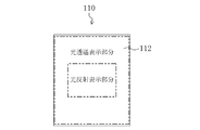
ここで、図16及び17に、上記特許文献1又は2に記載した従来の垂直配向モードを構成する半透過型の液晶表示装置の画素構造100を示す。画素構造100は、光反射表示部分と光透過表示部分とがその画素内にそれぞれ独立して形成されている。そして、領域ごとに配向制御手段101が設けられて配向制御がなされているため、画素電極102を分割して領域ごとに配置しなければならない。この場合、各領域で配向制御のための電界の勾配を形成するため、光反射表示部分と光透過表示部分との間で画素電極が存在しない開口部を設ける必要がある。そのためには、画素電極のくびれ部103を設ける必要がある。
Here, FIGS. 16 and 17 show a
しかし、光反射表示部分と光透過表示部分との間に画素電極102のくびれ部103を設けると、くびれ部の領域の画素電極が他領域のものに比べて細くなる。このため、製造工程や使用時の熱膨張・熱収縮等により断切れが発生し、表示品位が低下するおそれがあるという問題がある。
However, when the
また、画素電極102にくびれ部103を設けることにより形成された開口部、即ちくびれ部103の両側に形成された画素電極102が存在しない領域が生じると、図16に示すように表示領域内であるのに表示に寄与しない無効領域が発生してしまう。このため、開口率が減少するという問題もある。
Further, when an opening formed by providing the
さらに、図17に示すように、開口部、即ち画素電極が存在しない領域における下地配線104による電位が光反射表示部分及び光透過表示部分の配向制御に影響し、表示異常が発生するおそれがあるという問題もある。
Further, as shown in FIG. 17, the potential due to the
本発明は、斯かる諸点に鑑みてなされたものであり、その目的とするところは、表示品位が良好で且つ高開口率を実現する液晶表示装置を提供することである。 The present invention has been made in view of such various points, and an object of the present invention is to provide a liquid crystal display device which has a good display quality and realizes a high aperture ratio.
本発明に係る液晶表示装置は、互いに対向するように設けられた第1基板及び第2基板と、第1基板と該第2基板との間に挟持された液晶層を有し、液晶層は、負の誘電異方性を有する液晶材料で形成されており、電圧無印加状態において、液晶材料の液晶分子は、第1基板及び第2基板に概ね垂直に配向し、液晶表示パネルの表示領域が複数の画素で構成された液晶表示装置であって、複数の画素のそれぞれは、表示面側からの光を反射して表示を行う光反射表示部分と、背面側からの光を透過して表示を行う光透過表示部分と、を有すると共に、光反射表示部分及び光透過表示部分のいずれか一方が他方を囲むように設けられ、液晶層に電圧を印加したときに液晶層の液晶分子を軸対称配向させる配向制御手段が画素の中央部に設けられていることを特徴とする。 The liquid crystal display device according to the present invention includes a first substrate and a second substrate provided so as to face each other, and a liquid crystal layer sandwiched between the first substrate and the second substrate, The liquid crystal material is formed of a liquid crystal material having negative dielectric anisotropy, and in a state where no voltage is applied, the liquid crystal molecules of the liquid crystal material are aligned substantially perpendicularly to the first substrate and the second substrate, and the display region of the liquid crystal display panel Is a liquid crystal display device composed of a plurality of pixels, and each of the plurality of pixels reflects a light from a display surface and displays a light reflection display portion and transmits light from a back surface. A light-transmitting display portion that performs display, and one of the light-reflecting display portion and the light-transmitting display portion is provided so as to surround the other, and the liquid crystal molecules of the liquid crystal layer are arranged when a voltage is applied to the liquid crystal layer. An alignment control means for axisymmetric alignment is provided at the center of the pixel. And said that you are.
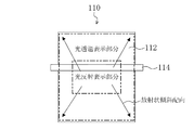
ここで、図18及び19に、本発明に係る液晶表示装置の表示部分の構造110の概略を示す。このような構成によれば、液晶表示パネルの複数の画素のそれぞれが、光反射表示部分及び光透過表示部分のいずれか一方が他方を囲むように設けられているため、画素電極112に開口部を設けるためのくびれ部が存在しない。従って、画素電極112が細く形成された領域がないためその部分で生じていた断切れが発生せず、表示品位の低下を回避することができる。
18 and 19 schematically show the
また、画素電極112にくびれ部を設けて開口部を形成する必要がなく表示領域内に表示に寄与しない無効領域が発生しない。従って、開口率の減少を回避することができる。
In addition, it is not necessary to provide a constricted portion in the
さらに、表示領域内に画素電極112が存在しない無効領域がないため、下地配線114の電位による影響を受けることがなく、表示異常が発生しない。
Further, since there is no invalid area in which the
また、本発明に係る液晶表示装置は、光透過表示部分が光反射表示部分を囲むように設けられており、光反射表示部分が光透過表示部分の中央部に形成されていてもよい。 In the liquid crystal display device according to the present invention, the light transmissive display portion may be provided so as to surround the light reflective display portion, and the light reflective display portion may be formed at the center of the light transmissive display portion.
このような構成によれば、光反射表示部分が光透過表示部分の中央部に形成されているため、図19に示すように、配向制御手段から放射状に液晶分子を配向させる際に画素全体にバランス良く液晶分子を配向させることができる。従って、表示品位がより良好となる。 According to such a configuration, since the light reflection display portion is formed in the central portion of the light transmission display portion, as shown in FIG. 19, when the liquid crystal molecules are aligned radially from the alignment control means, Liquid crystal molecules can be aligned with a good balance. Therefore, the display quality becomes better.
さらに、本発明に係る液晶表示装置は、光反射表示部分が光透過表示部分を囲むように設けられており、光透過表示部分が光反射表示部分の中央部に形成されていてもよい。 Furthermore, in the liquid crystal display device according to the present invention, the light reflective display portion may be provided so as to surround the light transmissive display portion, and the light transmissive display portion may be formed at the center of the light reflective display portion.
このような構成によれば、光透過表示部分が光反射表示部分の中央部に形成されているため、上述のように、配向制御手段から放射状に液晶分子を配向させる際に画素全体にバランス良く液晶分子を配向させることができる。従って、表示品位がより良好となる。 According to such a configuration, since the light transmissive display portion is formed in the central portion of the light reflective display portion, as described above, when the liquid crystal molecules are aligned radially from the alignment control means, the entire pixel is well balanced. Liquid crystal molecules can be aligned. Therefore, the display quality becomes better.
また、本発明に係る液晶表示装置は、光反射表示部分の外形と光透過表示部分の外形とが相似であってもよい。 In the liquid crystal display device according to the present invention, the outer shape of the light reflection display portion and the outer shape of the light transmission display portion may be similar.
このような構成によれば、光反射表示部分の外形と光透過表示部分の外形とが相似であるため、配向制御手段から放射状に液晶分子を配向させる際に画素全体にバランス良く行うことができ、表示品位が向上する。 According to such a configuration, since the outer shape of the light reflection display portion and the outer shape of the light transmission display portion are similar, when the liquid crystal molecules are aligned radially from the alignment control means, the entire pixel can be balanced. , Display quality is improved.
さらに、本発明に係る液晶表示装置は、光反射表示部分及び光透過表示部分がいずれも外形が正方形であってもよい。 Further, in the liquid crystal display device according to the present invention, the light reflection display portion and the light transmission display portion may both have a square outer shape.
このような構成によれば、光反射表示部分及び光透過表示部分がいずれも外形が正方形であるため、光反射表示部分の中心から光透過表示部分の端までバランス良く液晶分子を配向させることができる。従って、表示品位がより良好となる。 According to such a configuration, since both the light reflection display portion and the light transmission display portion have a square outer shape, liquid crystal molecules can be aligned in a balanced manner from the center of the light reflection display portion to the end of the light transmission display portion. it can. Therefore, the display quality becomes better.
また、本発明に係る液晶表示装置は、光反射表示部分の外形が六角形であると共に、光透過表示部分の外形が円形であってもよい。 In the liquid crystal display device according to the present invention, the outer shape of the light reflection display portion may be a hexagon and the outer shape of the light transmission display portion may be a circle.
このような構成によれば、光反射表示部分の外形が六角形であると共に、光透過表示部分の外形が円形であるため、光反射表示部分の端から光透過表示部分の中心までバランス良く液晶分子を配向させることができる。従って、表示品位がより良好となる。 According to such a configuration, since the outer shape of the light reflective display portion is hexagonal and the outer shape of the light transmissive display portion is circular, the liquid crystal is well balanced from the end of the light reflective display portion to the center of the light transmissive display portion. The molecules can be oriented. Therefore, the display quality becomes better.
さらに、本発明に係る液晶表示装置は、配向制御手段が光反射表示部分の中央部に形成されていてもよい。 Furthermore, in the liquid crystal display device according to the present invention, the orientation control means may be formed at the center of the light reflection display portion.
このような構成によれば、配向制御手段が光反射表示部分の中央部に形成されているため、表示部分の中心部を配向の中心として全体に亘りバランス良く放射状に液晶分子を配向させることができ、表示品位が向上する。 According to such a configuration, since the alignment control means is formed in the central portion of the light reflection display portion, the liquid crystal molecules can be aligned radially in a well-balanced manner with the central portion of the display portion as the center of alignment. Display quality is improved.
また、本発明に係る液晶表示装置は、配向制御手段が第1基板又は第2基板に形成された凸部であってもよい。 In the liquid crystal display device according to the present invention, the alignment control means may be a convex portion formed on the first substrate or the second substrate.
このような構成によれば、通常のパターン処理等によって凸部を形成すればよく、既存の設備を用いて容易に配向制御手段を形成することができる。 According to such a configuration, the convex portion may be formed by a normal pattern process or the like, and the orientation control means can be easily formed using existing equipment.
さらに、本発明に係る液晶表示装置は、配向制御手段が第1基板又は第2基板に形成された切り欠き部であってもよい。 Further, in the liquid crystal display device according to the present invention, the alignment control means may be a notch formed in the first substrate or the second substrate.
このような構成によれば、通常のパターン処理等によって切り欠き部を形成すればよく、既存の設備を用いて容易に配向制御手段を形成することができる。 According to such a configuration, the cutout portion may be formed by ordinary pattern processing or the like, and the orientation control means can be easily formed using existing equipment.
また、本発明に係る液晶表示装置は、複数の画素のそれぞれが第1基板の第1電極及び第2基板の第2電極を有し、切り欠き部が第1電極又は第2電極に形成されていてもよい。 In the liquid crystal display device according to the present invention, each of the plurality of pixels includes the first electrode of the first substrate and the second electrode of the second substrate, and the notch is formed in the first electrode or the second electrode. It may be.
このような構成によれば、画素電極のパターン処理の際に同時に配向制御手段を形成することができる。従って、製造コスト及び製造効率が良好となる。 According to such a configuration, the orientation control means can be formed simultaneously with the pattern processing of the pixel electrode. Therefore, manufacturing cost and manufacturing efficiency are improved.
以上説明したように、本発明によれば、表示品位が良好で且つ高開口率を実現する液晶表示装置を提供することができる。 As described above, according to the present invention, it is possible to provide a liquid crystal display device that has a good display quality and realizes a high aperture ratio.
以下、本発明の実施形態1〜8に係る液晶表示装置を図面に基づいて詳細に説明する。尚、本発明は、以下の実施形態に限定されるものではない。また、実施形態1〜8に係る液晶表示装置はいずれも透過モードの表示と反射モードの表示の両方を行うことのできる半透過型の液晶表示装置である。さらに、以下、画素内において、表示面側からの光を反射して表示を行う部分を光反射表示部分と、光反射表示部分を囲むように設けられ背面側からの光を透過して表示を行う部分を光透過表示部分と記載する。 Hereinafter, liquid crystal display devices according to Embodiments 1 to 8 of the present invention will be described in detail with reference to the drawings. The present invention is not limited to the following embodiment. The liquid crystal display devices according to Embodiments 1 to 8 are all transflective liquid crystal display devices that can perform both transmission mode display and reflection mode display. Further, in the following, in the pixel, a portion that performs display by reflecting light from the display surface side is provided so as to surround the light reflection display portion and the light reflection display portion, and light is transmitted from the back side for display. A portion to be performed is referred to as a light transmission display portion.
(実施形態1)
(液晶表示装置10の構成)
図1に、本実施形態1に係る液晶表示装置10の1つの画素構成の断面図を示す。また、図2は液晶表示装置10の1つの画素構成の平面図を示す。
(Embodiment 1)
(Configuration of the liquid crystal display device 10)
FIG. 1 shows a cross-sectional view of one pixel configuration of the liquid
液晶表示装置10は、対向する薄膜トランジスタ基板(TFT基板11)及びカラーフィルタ基板(CF基板12)、それらの間に設けられた液晶層13を有する液晶表示パネル14、及び、不図示のバックライト等から構成されている。
The liquid
TFT基板11は、絶縁性基板15、絶縁性基板15の表面に形成された回路要素、絶縁性基板15上に形成された反射膜16、反射膜16を覆うように形成された透明絶縁層17、透明絶縁層17上に設けられた画素電極18及び画素電極18上に形成された不図示の垂直配向膜で構成されている。
The
TFT基板11には、いずれも不図示のゲート電極、ソース電極及びドレイン電極等で構成される薄膜トランジスタ89が形成されている。ゲート電極は走査配線90に、ドレイン電極は信号配線91に、またソース配線は画素電極18に接続されている。TFT基板11は、各画素電極18内に蓄積容量を設けている。蓄積容量は、画素電極18と参照電極配線92で構成されている。
A
反射膜16は、絶縁性基板15上に、平面視で正方形状に形成されている。反射膜16によって表示部分93内の光反射表示部分130が規定される。従って、本実施形態の場合、光反射表示部分130は正方形状となる。反射膜16は、凹凸形状に形成された樹脂層上にAl層等が蒸着されることで、その表面が凹凸状に形成されている。反射膜16は、画素電極18の中央部に形成されている。
The
透明絶縁層17は、反射膜16を覆うように形成されて、反射膜16の凹凸形状を表面において平坦化している。
The transparent insulating
画素電極18は、透明絶縁層17の平坦な表面上に形成されている。画素電極18は、ITO(Indium Tin Oxide)等を用いて形成されており、透明電極を構成している。画素電極18は、所定の位置に形成された切り欠き部95を有しており、各画素は、この切り欠き部95によって図2に示すような正方形の画素パターンに分割されている。画素電極18によって表示部分93が規定される。液晶層13に所定の電圧を印加すると、画素電極18の周囲及び切り欠き部95の近傍に生成される斜め電界の配向規制によって、複数の画素パターンのそれぞれに放射状傾斜配向を施す液晶ドメインが形成される。
The
CF基板12は、ガラス等で形成された絶縁性基板96、絶縁性基板96上に形成されたCF層97、CF層97上に形成された透明誘電体層98、CF層97上及び透明誘電体層98上にそれぞれ形成された対向電極99、対向電極99上に形成された凸部120(配向制御手段)及び対向電極99及び凸部120上に形成された不図示の垂直配向膜で構成されている。
The
CF層97は、赤(R)、緑(G)及び青(B)の3原色からなる画素パターンで構成されている。これらの画素パターンは、その間に、コントラストを得るための縁取りとしてブラックマトリクス121が設けられている。そして、このブラックマトリクス121で画素パターンが区切られている。ブラックマトリクス121で区切られた画素パターンは、TFT基板11上の正方形の画素電極18と同形状且つ直上に形成されている。即ち、表示部分93を平面視した際に画素パターンと画素電極18とが同一に重なって見えるような位置にそれぞれ形成されている。また、画素パターンを構成するものとしては、RGBの組合せ以外に、シアン、マゼンタ、イエローの補色を用いてもよく、無色としてもよい。
The
透明誘電体層98は、CF基板12の光反射表示部分130に形成されている。透明誘電体層98は、TFT基板11上の正方形の反射膜16と同形状且つ直上に形成されている。即ち、光反射表示部分130を平面視した際に透明誘電体層98と反射膜16とが同一に重なって見えるような位置に形成されている。透明誘電体層98は、所定の厚さをもって切頭四角錐状に形成されている。透明誘電体層98に対応する液晶層13の厚さbは、液晶層13の厚さaの略半分程度であるのが好ましい。反射モードの表示では、表示に用いられる光は液晶層13を2回通過するのに対し、透過モードの表示では、表示に用いられる光は液晶層13を1回通過するだけである。従って、光透過表示部分131の液晶層13の厚さaを光反射表示部分130の液晶層13の厚さbの略2倍に設定すると、両者の光路長が等しくなり、両方の表示モードで良好な表示を実現できる。
The
対向電極99は、CF層97上及び透明誘電体層98上にそれぞれ形成されている。対向電極99は、ITO等を用いて形成されており、透明電極を構成している。
The
凸部120は、対向電極99上で、且つ、透明誘電体層98の中央部、即ち、光反射表示部分130の中央部に形成されている。凸部120は、その構成材料は特に限定されず、樹脂製材料、セラミック製又は金属製の材料であってもよい。また、凸部120は、対向するTFT基板11へ延びるような切頭円錐状に形成されており、その頭頂部とTFT基板11との間に間隙が形成されている。凸部120は、その形状は限定されず、円錐形状、角錐形状又は切頭角錐形状等に形成されていてもよい。
The
液晶層13は、TFT基板11及びCF基板12の間に設けられている。液晶層13は、誘電異方性が負のネマティック液晶材料を含み、必要に応じてカイラル剤をさらに含む。液晶層13は、電圧無印加状態において、その液晶材料の液晶分子がTFT基板11及びCF基板12に概ね垂直に配向されている。
The
(液晶表示装置10の製造方法)
次に、液晶表示装置10の製造方法について説明する。
(Manufacturing method of the liquid crystal display device 10)
Next, a method for manufacturing the liquid
(CF基板12の製造方法)
まず、絶縁性基板96を用意する。そして、絶縁性基板96上の遮光部分となる領域に幅5〜50μmのブラックマトリクス121をスパッタリング法により形成する。次に、絶縁性基板96上の表示部分93となる領域に赤の顔料が分散された樹脂フィルム(ドライフィルム)を全面にラミネートし、露光、現像及びベーク(熱処理)を行って、第1色層122(赤)を形成する。次に、第1色層122に重ねて、緑色の顔料が分散された樹脂フィルムを全面にラミネートし、露光、現像及びベーク(熱処理)を行って、第2色層122(緑)を形成する。同様に、第3色層122(青)を形成する。
(Manufacturing method of CF substrate 12)
First, an insulating
尚、色層122は、ストライプ配列となるように形成してもよく、デルタ配列であってもよい。また、色層122の形成方法は、ドライフィルムをラミネートする代わりに、顔料が分散された感光性樹脂材料をスピン、スリットコートにより全面に塗布してもよい。更に、着色層122の各色の形成順序は、特に限定されず、他の順序でもよい。
The
次に、色層122上の光反射表示部分130となる領域に透明誘電体層98を形成する。
Next, a
次いで、色層122、ブラックマトリクス121及び透明誘電体層98上にITOを蒸着し、対向電極99を形成する。
Next, ITO is deposited on the
次に、凸部120を透明誘電体層98の中央部に位置するように対向電極99上に形成する。凸部120は、フォトリソグラフィ法により形成される。
Next, the
次いで、対向電極99上に垂直配向膜を形成する。
Next, a vertical alignment film is formed on the
以上の工程により、CF基板12が完成する。
The
(TFT基板11の製造工程)
続いて、絶縁性基板15を用意し、Ta又はAl/Tiからなるゲート電極をスパッタ法により形成し、パターニングする。次に、ゲート絶縁膜としてSiNx、薄膜として半導体a−Siを形成する。次いで、エッチング保護膜としてSiNxを形成し、パターン形成を行う。尚、薄膜トランジスタはP−Siあるいは単結晶Siでも良く、トランジスタ構造はトップゲート構造でもよい。次に、コンタクトホール、ドレイン電極及びソース電極を形成する。さらに、同一工程又は別工程によって、基板端部にドライバを設け、薄膜トランジスタ89を形成する。さらに、光反射表示部分130となる領域に反射膜16を形成し、パターン形成を行い、これらの上層に透明絶縁層17を形成する。次に、ITOを真空蒸着してさらにパターン形成し、所定の切り欠き部95を有する画素電極18を形成する。画素電極18は表示部分93となる領域に形成する。続いて、セル厚を規定するための柱状スペーサ(不図示)を、フォトリソグラフィ工程を経て表示部分93外の所定位置に複数形成する。なお、柱状スペーサはCF側に形成してもよく、表示部93内の所定位置に形成してもよく、また球状スペーサを散布する方式を用いてもよい。
(Manufacturing process of TFT substrate 11)
Subsequently, an insulating
(液晶表示パネル14の形成工程)
次に、ディスペンサ等を用いて、例えば1ショット当り2mgの液晶材料をTFT基板11に滴下する。この際、液晶材料はTFT基板11の遮光領域外周囲に枠状に塗布されたシール剤の内方に滴下する。続いて、液晶材料が滴下されたTFT基板11にCF基板12を位置合わせして貼り付ける。この工程は真空中で行われる。次いで、大気中に戻すと貼り合わされたTFT基板11及びCF基板12間の液晶材料が大気圧により拡散する。次に、シール剤の塗布領域に沿ってUV光源を移動させながらUV光をシール剤に照射し、シール剤を硬化させる。このようにして、拡散した液晶材料は2枚の基板間に封止されて液晶表示パネル14を形成し、これに不図示のバックライトユニット等を設けて液晶表示装置10を完成させる。
(Formation process of the liquid crystal display panel 14)
Next, for example, 2 mg of liquid crystal material per shot is dropped onto the
また、液晶表示パネル14は、本実施形態のように形成されなくてもよく、液晶表示パネル14の側方に液晶注入口を設けて、そこへ液晶材料を注入し、その後液晶注入口を紫外線硬化樹脂等で封止するものであってもよい。 Further, the liquid crystal display panel 14 may not be formed as in the present embodiment. A liquid crystal injection port is provided on the side of the liquid crystal display panel 14 and a liquid crystal material is injected therein. It may be sealed with a cured resin or the like.
(実施形態2)
(液晶表示装置20の構成)
図5に、本実施形態2に係る液晶表示装置20の1つの画素構成の断面図を示す。また、上記実施形態で示したものと同様の部分については同符号を付し、その説明を省略する。
(Embodiment 2)
(Configuration of the liquid crystal display device 20)
FIG. 5 shows a cross-sectional view of one pixel configuration of the liquid
液晶表示装置20は、対向するTFT基板11及びCF基板22、それらの間に設けられた液晶層13を有する液晶表示パネル24、及び、不図示のバックライト等から構成されている。
The liquid
CF基板22は、ガラス等で形成された絶縁性基板96、絶縁性基板96上に形成されたCF層97、CF層97上に形成された透明誘電体層98、CF層97上及び透明誘電体層98上にそれぞれ形成された対向電極99及び対向電極99上に形成された不図示の垂直配向膜で構成されている。
The
対向電極99は、CF層97上及び透明誘電体層98上にそれぞれ形成されている。対向電極99は、透明誘電体層98上の中央部に円形状の切り欠き部25(配向制御手段)が形成されている。切り欠き部25は円形状でなくてもよく、楕円形状や多角形状に形成されていてもよい。
The
(液晶表示装置20の製造方法)
次に、液晶表示装置20の製造方法について説明する。
(Manufacturing method of the liquid crystal display device 20)
Next, a method for manufacturing the liquid
(CF基板22の製造方法)
まず、実施形態1と同様にして、絶縁性基板96上に色層122、ブラックマトリクス121及び透明誘電体層98を形成する。次に、透明誘電体層98上にITOを蒸着し、対向電極99を形成する。
(Manufacturing method of CF substrate 22)
First, the
次いで、透明誘電体層98の中央部に円形状の切り欠き部25が位置するように対向電極99をパターニングし、さらに、対向電極99上に垂直配向膜を形成する。以上の工程により、CF基板22が完成する。
Next, the
(TFT基板11の製造工程)
続いて、実施形態1と同様にして、TFT基板11を形成する。
(Manufacturing process of TFT substrate 11)
Subsequently, the
(液晶表示パネル24の形成工程)
次に、実施形態1と同様にして、液晶材料を2枚の基板間に設けて封止した液晶表示パネル24を形成し、これに不図示のバックライトユニット等を設けて液晶表示装置20を完成させる。
(Formation process of the liquid crystal display panel 24)
Next, in the same manner as in the first embodiment, a liquid crystal display panel 24 in which a liquid crystal material is provided between two substrates and sealed is formed. Finalize.
(実施形態3)
(液晶表示装置30の構成)
図6に、本実施形態3に係る液晶表示装置30を示す。また、上記実施形態で示したものと同様の部分については同符号を付し、その説明を省略する。
(Embodiment 3)
(Configuration of the liquid crystal display device 30)
FIG. 6 shows a liquid
液晶表示装置30は、対向するTFT基板11及びCF基板32、それらの間に設けられた液晶層13を有する液晶表示パネル34、及び、不図示のバックライト等から構成されている。
The liquid
CF基板32は、ガラス等で形成された絶縁性基板96、絶縁性基板96上に形成されたCF層97、CF層97上に形成された透明誘電体層98、CF層97上及び透明誘電体層98上にそれぞれ形成された対向電極99及び対向電極99上に形成された不図示の垂直配向膜で構成されている。
The
対向電極99は、CF層97上及び透明誘電体層98上にそれぞれ形成されており、さらにその上には垂直配向膜が形成されている。
The
CF基板32の垂直配向膜、対向電極99及びその直下の透明誘電体層98には、それらの厚さ方向に亘って切り欠き部35(配向制御手段)が形成されている。切り欠き部35は、透明誘電体層98内に頂点を有し、垂直配向膜の表面に底辺を有する円錐形状に形成されている。切り欠き部35は、透明誘電体層98上の中央部に位置するように形成されている。切り欠き部35は円錐形状でなくてもよく、切頭円錐形状、角錐形状又は切頭角錐形状等に形成されていてもよい。
In the vertical alignment film of the
(液晶表示装置30の製造方法)
次に、液晶表示装置30の製造方法について説明する。
(Manufacturing method of the liquid crystal display device 30)
Next, a method for manufacturing the liquid
(CF基板32の製造方法)
まず、実施形態1と同様にして、絶縁性基板96上に色層122、ブラックマトリクス121及び透明誘電体層98を形成する。次に、透明誘電体層98上にITOを蒸着し、対向電極99を形成し、さらに対向電極99上に垂直配向膜を形成する。次いで、透明誘電体層98の中央部に円錐形状の切り欠き部35が位置するように垂直配向膜、対向電極99及び透明誘電体層98をパターニングする。
(Manufacturing method of CF substrate 32)
First, the
以上の工程により、CF基板32が完成する。
The
(TFT基板11の製造工程)
続いて、実施形態1と同様にして、TFT基板11を形成する。
(Manufacturing process of TFT substrate 11)
Subsequently, the
(液晶表示パネル34の形成工程)
次に、実施形態1と同様にして、液晶材料を2枚の基板間に設けて封止した液晶表示パネル34を形成し、これに不図示のバックライトユニット等を設けて液晶表示装置30を完成させる。
(Formation process of the liquid crystal display panel 34)
Next, in the same manner as in the first embodiment, a liquid
(実施形態4)
(液晶表示装置40の構成)
図7に、本実施形態4に係る液晶表示装置40を示す。また、上記実施形態で示したものと同様の部分については同符号を付し、その説明を省略する。
(Embodiment 4)
(Configuration of the liquid crystal display device 40)
FIG. 7 shows a liquid
液晶表示装置40は、対向するTFT基板41及びCF基板42、それらの間に設けられた液晶層13を有する液晶表示パネル44、及び、不図示のバックライト等から構成されている。
The liquid
TFT基板41は、絶縁性基板15、絶縁性基板15の表面に形成された回路要素、絶縁性基板15上に形成された反射膜16、反射膜16を覆うように形成された透明絶縁層17、透明絶縁層17上に設けられた画素電極18及び画素電極18上に形成された不図示の垂直配向膜で構成されている。
The
画素電極18は、透明絶縁層17の平坦な表面上に形成されている。画素電極18は、所定の位置に形成された切り欠き部95を有しており、各画素は、この切り欠き部95によって図2に示すような正方形の画素パターンに分割されている。画素電極18によって表示部分93が規定される。液晶層13に所定の電圧を印加すると、画素電極18の周囲及び切り欠き部95の近傍に生成される斜め電界の配向規制によって、複数の画素パターンのそれぞれに放射状傾斜配向を施す液晶ドメインが形成される。画素電極18は、画素中央部、即ち表示部分93の中央部に円形状の切り欠き部45(配向制御手段)が形成されている。切り欠き部45は円形状でなくてもよく、楕円形状や多角形状に形成されていてもよい。
The
CF基板42は、ガラス等で形成された絶縁性基板96、絶縁性基板96上に形成されたCF層97、CF層97上に形成された透明誘電体層98、CF層97上及び透明誘電体層98上にそれぞれ形成された対向電極99、対向電極99上に形成された不図示の垂直配向膜で構成されている。
The
(液晶表示装置40の製造方法)
次に、液晶表示装置40の製造方法について説明する。
(Manufacturing method of the liquid crystal display device 40)
Next, a method for manufacturing the liquid
(CF基板42の製造方法)
まず、実施形態1と同様に、絶縁性基板96を用意し、絶縁性基板96上の遮光部分となる領域にブラックマトリクス121を、絶縁性基板96上の表示部分93となる領域に色層122を、それぞれ形成する。次に、色層122上の光反射表示部分130となる領域に透明誘電体層98を形成する。次いで、色層122、ブラックマトリクス121及び透明誘電体層98上にITOを蒸着し、対向電極99を形成し、次いで対向電極99上に垂直配向膜を形成する。以上の工程により、CF基板42が完成する。
(Manufacturing method of CF substrate 42)
First, as in the first embodiment, an insulating
(TFT基板41の製造工程)
続いて、絶縁性基板15を用意し、実施形態1と同様にして回路要素を設ける。さらに、光反射表示部分130となる領域に反射膜16を形成し、パターン形成を行い、これらの上層に層間絶縁膜を形成する。次に、ITOを真空蒸着してさらにパターン形成し、所定の切り欠き部45を有する画素電極18を形成する。画素電極18は表示部分93となる領域に形成する。
(Manufacturing process of TFT substrate 41)
Subsequently, an insulating
ここで、切り欠き部45は、表示部分93を規定するように各画素単位に区切るために設けるもの、及び、配向制御手段として表示部分93の中央部に設けるためのものをそれぞれ同時に形成する。
Here, the
続いて、セル厚を規定するための柱状スペーサを、フォトリソグラフィ工程を経て表示部分93外の所定位置に複数形成する。
Subsequently, a plurality of columnar spacers for defining the cell thickness are formed at predetermined positions outside the
(液晶表示パネル44の形成工程)
次に、実施形態1と同様にして、液晶材料を2枚の基板間に設けて封止した液晶表示パネル44を形成し、これに不図示のバックライトユニット等を設けて液晶表示装置40を完成させる。
(Formation process of the liquid crystal display panel 44)
Next, in the same manner as in the first embodiment, a liquid
(実施形態5)
(液晶表示装置50の構成)
図8に、本実施形態5に係る液晶表示装置50を示す。また、上記実施形態で示したものと同様の部分については同符号を付し、その説明を省略する。
(Embodiment 5)
(Configuration of the liquid crystal display device 50)
FIG. 8 shows a liquid
液晶表示装置50は、対向するTFT基板51及びCF基板42、それらの間に設けられた液晶層13を有する液晶表示パネル54、及び、不図示のバックライト等から構成されている。
The liquid
TFT基板51は、絶縁性基板15、絶縁性基板15の表面に形成された回路要素、絶縁性基板15上に形成された透明絶縁層56及び遮光層57、透明絶縁層56上に設けられた画素電極18、画素電極18上に形成された反射膜16、透明絶縁層17及び不図示の垂直配向膜で構成されている。
The
透明絶縁層56は、回路要素が形成された絶縁性基板15上に形成されている。透明絶縁層56は表示部分93の中央部が円形状に欠損しており、ここに遮光層57が形成されている。このため、遮光層57も円形状に形成されている。
The transparent insulating
遮光層57は、後述するTFT基板51表面に形成した切り欠き部55(配向制御手段)の真下に位置して、反射層の切り欠き部55からの光洩れを規制する働きをするため、反射層の切り欠き部55と同一又はそれ以上の大きさに形成されている。
The
画素電極18は、透明絶縁層56上に形成されている。画素電極18は、所定の位置に形成された切り欠き部95を有しており、各画素は、この切り欠き部95によって図2に示すような正方形の画素パターンに分割されている。画素電極18によって表示部分93が規定される。液晶層13に所定の電圧を印加すると、画素電極18の周囲及び切り欠き部95の近傍に生成される斜め電界の配向規制によって、複数の画素パターンのそれぞれに放射状傾斜配向を施す液晶ドメインが形成される。
The
反射膜16は、画素電極18上でその中央部に平面視で正方形状に形成されている。反射膜16によって表示部分93内の光反射表示部分130が規定される。従って、本実施形態の場合、光反射表示部分130は正方形状となる。反射膜16は、凹凸形状に形成された樹脂層上にAl層等が蒸着されることで、その表面が凹凸状に形成されている。
The
透明絶縁層17は、反射膜16を覆うように形成されて、反射膜16の凹凸形状を表面において平坦化している。
The transparent insulating
TFT基板51の透明絶縁層56及び反射膜16には、それらの厚さ方向に亘って切り欠き部55が形成されている。切り欠き部55は、反射膜16内に頂点を有し、透明絶縁層56の表面に底辺を有する円錐形状に形成されている。切り欠き部55は、反射膜16上であって、その中央部に位置するように形成されている。切り欠き部55は円錐形状でなくてもよく、切頭円錐形状、角錐形状又は切頭角錐形状等に形成されていてもよい。
A
CF基板42は、ガラス等で形成された絶縁性基板96、絶縁性基板96上に形成されたCF層97、CF層97上に形成された透明誘電体層98、CF層97上及び透明誘電体層98上にそれぞれ形成された対向電極99及び対向電極99上に形成された不図示の垂直配向膜で構成されている。
The
(液晶表示装置50の製造方法)
次に、液晶表示装置50の製造方法について説明する。
(Manufacturing method of the liquid crystal display device 50)
Next, a method for manufacturing the liquid
(CF基板42の製造方法)
まず、実施形態4と同様にして、CF基板42を作製する。
(Manufacturing method of CF substrate 42)
First, the
(TFT基板51の製造工程)
続いて、絶縁性基板15を用意し、実施形態1と同様にして回路要素を設け、この絶縁性基板15上に透明絶縁層56を形成した後、パターニングにより切り欠き部55を形成し、形成した切り欠き部55に遮光層57を設ける。
(Manufacturing process of TFT substrate 51)
Subsequently, an insulating
次に、ITOを真空蒸着してさらにパターン形成し、所定の切り欠き部95を有する画素電極18を形成する。画素電極18は表示部分93となる領域に形成する。
Next, ITO is vacuum-deposited and further patterned to form the
次いで、画素電極18上の光反射表示部分130となる領域に反射膜16を形成し、さらに透明絶縁層17を形成して表面を平坦化し、その上に垂直配向膜を形成する。
Next, the
続いて、反射部分の中央部に円錐形状の切り欠き部55が位置するように垂直配向膜、透明絶縁層17及び反射膜16をパターニングする。
Subsequently, the vertical alignment film, the transparent insulating
続いて、セル厚を規定するための柱状スペーサを、フォトリソグラフィ工程を経て表示部分93外の所定位置に複数形成する。
Subsequently, a plurality of columnar spacers for defining the cell thickness are formed at predetermined positions outside the
(液晶表示パネル54の形成工程)
次に、実施形態1と同様にして、液晶材料を2枚の基板間に設けて封止した液晶表示パネル54を形成し、これに不図示のバックライトユニット等を設けて液晶表示装置50を完成させる。
(Formation process of the liquid crystal display panel 54)
Next, in the same manner as in the first embodiment, a liquid
(実施形態6)
(液晶表示装置60の構成)
図9に、本実施形態6に係る液晶表示装置60を示す。また、上記実施形態で示したものと同様の部分については同符号を付し、その説明を省略する。
(Embodiment 6)
(Configuration of the liquid crystal display device 60)
FIG. 9 shows a liquid
液晶表示装置60は、対向するTFT基板61及びCF基板42、それらの間に設けられた液晶層13を有する液晶表示パネル64、及び、不図示のバックライト等から構成されている。
The liquid
TFT基板61は、絶縁性基板15、絶縁性基板15の表面に形成された回路要素、絶縁性基板15上に形成された透明絶縁層56、透明絶縁層56上に設けられた画素電極18、画素電極18上に形成された反射膜16、透明絶縁層17及び不図示の垂直配向膜で構成されている。
The
画素電極18は、透明絶縁層56上に形成されている。画素電極18は、所定の位置に形成された切り欠き部95を有しており、各画素は、この切り欠き部95によって図2に示すような正方形の画素パターンに分割されている。画素電極18によって表示部分93が規定される。液晶層13に所定の電圧を印加すると、画素電極18の周囲及び切り欠き部95の近傍に生成される斜め電界の配向規制によって、複数の画素パターンのそれぞれに放射状傾斜配向を施す液晶ドメインが形成される。
The
反射膜16は、画素電極18上でその中央部に平面視で正方形状に形成されている。反射膜16によって表示部分93内の光反射表示部分130が規定される。従って、本実施形態の場合、光反射表示部分130は正方形状となる。反射膜16は、凹凸形状に形成された樹脂層上にAl層等が蒸着されることで、その表面が凹凸状に形成されている。
The
透明絶縁層17は、反射膜16を覆うように形成されて、反射膜16の凹凸形状を表面において平坦化している。
The transparent insulating
凸部63(配向制御手段)は、透明絶縁層17上で、且つ、反射膜16の中央部、即ち、光反射表示部分130の中央部に形成されている。凸部63は、その構成材料は特に限定されず、樹脂製材料、セラミック製又は金属製の材料であってもよい。また、凸部63は、対向するCF基板42へ延びるような切頭円錐状に形成されており、その頭頂部とCF基板42との間に間隙が形成されている。凸部63は、その形状は限定されず、円錐形状、角錐形状又は切頭角錐形状等に形成されていてもよい。
The convex portion 63 (orientation control means) is formed on the transparent insulating
CF基板42は、ガラス等で形成された絶縁性基板96、絶縁性基板96上に形成されたCF層97、CF層97上に形成された透明誘電体層98、CF層97上及び透明誘電体層98上にそれぞれ形成された対向電極99、対向電極99上に形成された不図示の垂直配向膜で構成されている。
The
(液晶表示装置60の製造方法)
次に、液晶表示装置60の製造方法について説明する。
(Manufacturing method of the liquid crystal display device 60)
Next, a method for manufacturing the liquid
(CF基板42の製造方法)
まず、実施形態4と同様にして、CF基板42を作製する。
(Manufacturing method of CF substrate 42)
First, the
(TFT基板61の製造工程)
続いて、絶縁性基板15を用意し、実施形態1と同様にして回路要素を設け、この絶縁性基板15上に透明絶縁層56を形成する。
(Manufacturing process of TFT substrate 61)
Subsequently, an insulating
次に、ITOを真空蒸着してさらにパターン形成し、所定の切り欠き部95を有する画素電極18を形成する。画素電極18は表示部分93となる領域に形成する。
Next, ITO is vacuum-deposited and further patterned to form the
次いで、画素電極18上の光反射表示部分130となる領域に反射膜16を形成し、さらに透明絶縁層17を形成して表面を平坦化し、その上に垂直配向膜を形成する。
Next, the
続いて、凸部63を光反射部表示部分94の中央部に位置するように垂直配向膜上に形成する。凸部63は、フォトリソグラフィ法により形成される。
Subsequently, the
次に、セル厚を規定するための柱状スペーサを、フォトリソグラフィ工程を経て表示部分93外の所定位置に複数形成する。
Next, a plurality of columnar spacers for defining the cell thickness are formed at predetermined positions outside the
(液晶表示パネル64の形成工程)
次に、実施形態1と同様にして、液晶材料を2枚の基板間に設けて封止した液晶表示パネル64を形成し、これに不図示のバックライトユニット等を設けて液晶表示装置60を完成させる。
(Formation process of the liquid crystal display panel 64)
Next, in the same manner as in the first embodiment, a liquid
(実施形態7)
(液晶表示装置70の構成)
図10に、本実施形態7に係る液晶表示装置70を示す。また、上記実施形態で示したものと同様の部分については同符号を付し、その説明を省略する。
(Embodiment 7)
(Configuration of the liquid crystal display device 70)
FIG. 10 shows a liquid
液晶表示装置70は、対向するTFT基板11及びCF基板42、それらの間に設けられた液晶層13を有する液晶表示パネル74、及び、不図示のバックライト等から構成されている。
The liquid
TFT基板11は、絶縁性基板15、絶縁性基板15の表面に形成された回路要素、絶縁性基板15上に形成された反射膜16、反射膜16を覆うように形成された透明絶縁層17、透明絶縁層17上に設けられた画素電極18及び画素電極18上に形成された不図示の垂直配向膜で構成されている。
The
CF基板42は、ガラス等で形成された絶縁性基板96、絶縁性基板96上に形成されたCF層97、CF層97上に形成された透明誘電体層98、CF層97上及び透明誘電体層98上にそれぞれ形成された対向電極99及び対向電極99上に形成された不図示の垂直配向膜で構成されている。
The
透明誘電体層98は、側面がテーパ状に形成された切頭円錐形状に形成されている。透明誘電体層98は、光反射表示部分130の中央部に形成されており、この透明誘電体層98が配向制御手段を構成している。
The
(液晶表示装置70の製造方法)
液晶表示装置70は、実施形態4と同様にして作製したCF基板42と、実施形態1と同様にして作製したTFT基板11との間に液晶材料を設けて封止して液晶表示パネル74を形成し、これに不図示のバックライトユニット等を設けて完成させる。
(Manufacturing method of the liquid crystal display device 70)
In the liquid
(実施形態8)
(液晶表示装置80の構成)
図11に、本実施形態8に係る液晶表示装置80を示す。また、上記実施形態で示したものと同様の部分については同符号を付し、その説明を省略する。
(Embodiment 8)
(Configuration of the liquid crystal display device 80)
FIG. 11 shows a liquid
液晶表示装置80は、対向するTFT基板81及びCF基板22、それらの間に設けられた液晶層13を有する液晶表示パネル84、及び、不図示のバックライト等から構成されている。
The liquid
TFT基板81は、絶縁性基板15、絶縁性基板15の表面に形成された回路要素、絶縁性基板15上に形成された反射膜16、反射膜16を覆うように形成された透明絶縁層17、透明絶縁層17上に設けられた画素電極18、画素電極18上に形成された不図示の垂直配向膜及び凸部83で構成されている。
The TFT substrate 81 includes an insulating
凸部83は、画素電極18上の中央部、即ち、光反射表示部分130の中央部に形成されている。凸部83は、その構成材料は特に限定されず、樹脂製材料、セラミック製又は金属製の材料であってもよい。また、凸部83は、対向するCF基板22へ延びるような切頭円錐状に形成されており、その頭頂部とCF基板22との間に間隙が形成されている。この凸部83は、平面視においてCF基板22上に形成された切り欠き部25と重なる位置に形成されている。凸部83は、その形状は限定されず、円錐形状、角錐形状又は切頭角錐形状等に形成されていてもよい。
The
液晶表示装置80は、切り欠き部25と凸部83とが配向の中心に位置しており、これら両方の配向制御手段により配向制御を行っている。
In the liquid
尚、液晶表示装置80のように、TFT基板とCF基板との両基板上に配向制御手段をそれぞれ形成するものは、上記のようにTFT基板上に凸部があり、さらにCF基板の対向電極上に切り欠き部があるものに限らない。即ち、TFT基板の画素電極上に切り欠き部があり、さらにCF基板上に凸部があるものであってもよい。
Note that, as in the liquid
(液晶表示装置80の製造方法)
次に、液晶表示装置80の製造方法について説明する。
(Manufacturing method of the liquid crystal display device 80)
Next, a method for manufacturing the liquid
(CF基板22の製造方法)
実施形態2と同様にしてCF基板22を作製する。
(Manufacturing method of CF substrate 22)
The
(TFT基板81の製造工程)
続いて、実施形態1と同様にして、回路要素を設けた絶縁性基板15上の光反射表示部分130となる領域に反射膜16を形成し、パターン形成を行い、これらの上層に透明絶縁層17を形成する。次に、ITOを真空蒸着してさらにパターン形成し、所定の切り欠き部95を有する画素電極18を形成する。画素電極18は表示部分93となる領域に形成する。次いで、表示部分93の中央部に凸部83をパターニングにより形成する。続いて、セル厚を規定するための柱状スペーサを、フォトリソグラフィ工程を経て表示部分93外の所定位置に複数形成する。
(Manufacturing process of TFT substrate 81)
Subsequently, in the same manner as in the first embodiment, the
(液晶表示パネル84の形成工程)
次に、実施形態1と同様にして、液晶材料を2枚の基板間に設けて封止した液晶表示パネル84を形成し、これに不図示のバックライトユニット等を設けて液晶表示装置80を完成させる。
(Formation process of the liquid crystal display panel 84)
Next, in the same manner as in the first embodiment, a liquid
上記の液晶表示装置10〜80は、いずれも、画素電極18で規定される正方形の表示部分93の中央部に反射膜16で規定される正方形の光反射表示部分130が設けられている。このため、図2に示すように、光反射表示部分130を囲むように光透過表示部分131が位置することになる。
In each of the liquid
また、液晶表示装置10〜80は、各画素において配向制御を行う凸部120,63,83や切り欠き部25,35,45,55が光反射表示部分130の中央部に形成されている。このため、中央部の光反射表示部分130及びそれを囲む光透過表示部分131を合わせた1つの画素において、凸部120,63,83や切り欠き部25,35,45,55を画素内の中心として電圧を印加したときに液晶層13の液晶分子を軸対称配向させることができる。従って、表示装置の高コントラスト化及び広視野角化を実現できる。
Further, in the liquid
尚、光透過表示部分131及び光反射表示部分130の形状は、それぞれ正方形でなくてもよく、図3又は図4に示すように長方形であってもよい。ただし、この場合、それぞれが相似の関係となるような形状であるのが好ましい。
The shapes of the light
(実施形態9)
(液晶表示装置200の構成)
図12は本実施形態9に係る液晶表示装置200の1つの画素構成の平面図を、図13は液晶表示装置200の1つの画素構成の断面図を示す。また、上記実施形態で示したものと同様の部分については同符号を付し、その説明を省略する。
(Embodiment 9)
(Configuration of the liquid crystal display device 200)
12 is a plan view of one pixel configuration of the liquid
液晶表示装置200は、対向するTFT基板201及びCF基板202、それらの間に設けられた液晶層13を有する液晶表示パネル204、及び、不図示のバックライト等から構成されている。
The liquid
TFT基板201は、絶縁性基板15、絶縁性基板15の表面に形成された回路要素、絶縁性基板15上に形成された反射膜16、反射膜16を覆うように形成された透明絶縁層17、透明絶縁層17上に設けられた画素電極18、画素電極18上に形成された不図示の垂直配向膜で構成されている。
The
TFT基板201には、薄膜トランジスタ89が形成されており、そのゲート電極は走査配線90に、ドレイン電極は信号配線91に、またソース配線は画素電極18に接続されている。TFT基板201は、各画素電極18内に蓄積容量を設けている。蓄積容量は、画素電極18と参照電極配線92で構成されている。
A
反射膜16は、絶縁性基板15上に、平面視で中央に正方形状の切り欠きが形成された正方形状に形成されている。反射膜16によって表示部分93内の光反射表示部分210が規定される。従って、本実施形態の場合、光反射表示部分210は平面視で中央に正方形状の切り欠きが形成された正方形状になる。反射膜16は、凹凸形状に形成された樹脂層上にAl層等が蒸着されることで、その表面が凹凸状に形成されている。
The
CF基板202は、ガラス等で形成された絶縁性基板96、絶縁性基板96上に形成されたCF層97、CF層97上に形成された透明誘電体層98、CF層97上及び透明誘電体層98上にそれぞれ形成された対向電極99、対向電極99上に形成された凸部120(配向制御手段)及び対向電極99及び凸部120上に形成された不図示の垂直配向膜で構成されている。
The CF substrate 202 includes an insulating
透明誘電体層98は、CF基板12の光反射表示部分210に形成されている。透明誘電体層98は、TFT基板11上の反射膜16と同形状且つ直上に形成されている。即ち、光反射表示部分210を平面視した際に透明誘電体層98と反射膜16とが同一に重なって見えるような位置に形成されている。透明誘電体層98は、所定の厚さをもって切頭四角錐状に形成されている。透明誘電体層98に対応する液晶層13の厚さは、液晶層13の厚さaの略半分程度であるのが好ましい。
The
対向電極99は、CF層97上及び透明誘電体層98上にそれぞれ形成されている。対向電極99は、ITO等を用いて形成されており、透明電極を構成している。
The
光透過表示部分211は、光反射表示部分210の中央に形成された正方形状の切り欠きに位置している。
The light
凸部120は、対向電極99上で、且つ、光透過表示部分211の中央部に形成されている。
The
(液晶表示装置200の製造方法)
次に、液晶表示装置200の製造方法について説明する。
(Manufacturing method of the liquid crystal display device 200)
Next, a method for manufacturing the liquid
(CF基板202の製造方法)
まず、実施形態1と同様にして、色層122まで形成し、次に、色層122上の光反射表示部分210となる領域に透明誘電体層98を形成する。
(Manufacturing method of CF substrate 202)
First, in the same manner as in the first embodiment, the layers up to the
次いで、色層122、ブラックマトリクス121及び透明誘電体層98上にITOを蒸着し、対向電極99を形成する。
Next, ITO is deposited on the
次に、凸部120を光透過表示部分211の中央部に位置するように対向電極99上に形成する。凸部120は、フォトリソグラフィ法により形成する。
Next, the
次いで、対向電極99上に垂直配向膜を形成する。
Next, a vertical alignment film is formed on the
以上の工程により、CF基板202が完成する。 The CF substrate 202 is completed through the above steps.
(TFT基板201の製造工程)
続いて、実施形態1と同様の方法により薄膜トランジスタ89まで形成する。さらに、光反射表示部分210となる領域に反射膜16を形成し、パターン形成を行い、これらの上層に透明絶縁層17を形成する。次に、画素電極18を形成する。続いて、実施形態1と同様の方法によりセル厚を規定するための柱状スペーサ(不図示)を表示部分93外の所定位置に複数形成してTFT基板201を完成させる。
(Manufacturing process of TFT substrate 201)
Subsequently, up to the
続いて上述のように作製したCF基板202及びTFT基板201を用いて液晶表示装置200を完成させる。
Subsequently, the liquid
また、液晶表示装置200は、光透過表示部分211が正方形状に形成されているが、これに限らず、例えば、図14の液晶表示装置300のように光透過表示部分211が円形状に形成されていてもよい。さらに、図15の液晶表示装置400のように、光反射表示部分210の外形が六角形であると共に、光反射表示部分210の中央部の光透過表示部分211の外形が円形に形成されていてもよい。
Further, in the liquid
また、上述の実施形態1〜9において、光反射表示部分及び光透過表示部分のうち、一方が他方の中央部に形成されていたが、これに限られない。また、凸部や切り欠き部の位置も光反射表示部分或いは光透過表示部分の中央部に形成されていなくてもよい。 Moreover, in above-mentioned Embodiment 1-9, although one was formed in the other center part among the light reflection display parts and the light transmission display parts, it is not restricted to this. Further, the positions of the convex portions and the cutout portions may not be formed in the central portion of the light reflection display portion or the light transmission display portion.
さらに、上述の実施形態1〜9において、CF基板及びTFT基板の絶縁性基板は、それぞれその厚さは特に限定されず、TFT基板のほうが薄く形成されていてもよく、また、同じ厚さに形成されていてもよい。 Furthermore, in the above-described first to ninth embodiments, the thicknesses of the insulating substrates of the CF substrate and the TFT substrate are not particularly limited, and the TFT substrate may be formed thinner, and the same thickness may be used. It may be formed.
(作用効果)
次に、作用効果について説明する。
(Function and effect)
Next, operational effects will be described.
本実施形態に係る液晶表示装置10〜400は、互いに対向するように設けられたTFT基板11,41,51,61,81,201及びCF基板12,22,32,42,202と、それらの間に挟持された液晶層13を有し、液晶層13は、負の誘電異方性を有する液晶材料で形成されており、電圧無印加状態において、液晶材料の液晶分子は、TFT基板11,41,51,61,81,201及びCF基板12,22,32,42,202に概ね垂直に配向し、液晶表示パネル14〜204の表示領域が複数の画素で構成された液晶表示装置であって、複数の画素のそれぞれは、表示面側からの光を反射して表示を行う光反射表示部分130,210と、背面側からの光を透過して表示を行う光透過表示部分131,211と、を有すると共に、光反射表示部分及び光透過表示部分のいずれか一方が他方を囲むように設けられ、液晶層13に電圧を印加したときに液晶層13の液晶分子を軸対称配向させる配向制御手段(凸部120,63,83又は/及び切り欠き部25,35,45,55)が画素の中央部に設けられていることを特徴とする。
The liquid
このような構成によれば、液晶表示パネル14〜204の複数の画素のそれぞれが、光反射表示部分130,210とそれを囲むように設けられた光透過表示部分131,211とを有しているため、画素電極18に開口部を設けるためのくびれ部が存在しない。従って、画素電極18が細く形成された領域がないためその部分で生じていた断切れが発生せず、表示品位の低下を回避することができる。
According to such a configuration, each of the plurality of pixels of the liquid crystal display panels 14 to 204 includes the light
また、画素電極18にくびれ部を設けて開口部を形成する必要がなく表示領域内に表示に寄与しない無効領域が発生しない。従って、開口率の減少を回避することができる。
In addition, it is not necessary to provide a constricted portion in the
さらに、表示領域内に画素電極18が存在しない無効領域がないため、下地配線の電位による影響を受けることがなく、表示異常が発生しない。
Furthermore, since there is no invalid area in which the
また、本実施形態に係る液晶表示装置10〜80は、光透過表示部分131が光反射表示部分130を囲むように設けられており、光反射表示部分130が光透過表示部分131の中央部に形成されていることを特徴とする。
Further, in the liquid
このような構成によれば、光反射表示部分130が光透過表示部分131の中央部に形成されているため、配向制御手段から放射状に液晶分子を配向させる際に画素全体にバランス良く液晶分子を配向させることができる。従って、表示品位がより良好となる。
According to such a configuration, since the light
さらに、本実施形態に係る液晶表示装置200〜400は、光反射表示部分211が光透過表示部分210を囲むように設けられており、光透過表示部分211が光反射表示部分210の中央部に形成されていることを特徴とする。
Further, in the liquid
このような構成によれば、光透過表示部分211が光反射表示部分210の中央部に形成されているため、上述のように、配向制御手段から放射状に液晶分子を配向させる際に画素全体にバランス良く液晶分子を配向させることができる。従って、表示品位がより良好となる。
According to such a configuration, since the light
また、本実施形態に係る液晶表示装置10〜200は、光反射表示部分130,210の外形と光透過表示部分131,211の外形とが相似であることを特徴とする。
Further, the liquid
このような構成によれば、光反射表示部分130,210の外形と光透過表示部分131,211の外形とが相似であるため、配向制御手段(凸部120,63,83又は/及び切り欠き部25,35,45,55)から放射状に液晶分子を配向させる際に画素全体にバランス良く行うことができ、表示品位が向上する。
According to such a configuration, the outer shape of the light
さらに、本実施形態に係る液晶表示装置10〜200は、光反射表示部分130,210及び光透過表示部分131,211がいずれも外形が正方形であることを特徴とする。
Furthermore, the liquid
このような構成によれば、光反射表示部分130,210及び光透過表示部分131,211がいずれも外形が正方形であるため、光反射表示部分130,210の中心から光透過表示部分131,211の端までバランス良く液晶分子を配向させることができる。従って、表示品位がより良好となる。
According to such a configuration, since the light
また、本発明に係る液晶表示装置400は、光反射表示部分210の外形が六角形であると共に、光透過表示部分211の外形が円形であることを特徴とする。
Further, the liquid
このような構成によれば、光反射表示部分210の外形が六角形であると共に、光透過表示部分211の外形が円形であるため、光反射表示部分210の端から光透過表示部分211の中心までバランス良く液晶分子を配向させることができる。従って、表示品位がより良好となる。
According to such a configuration, since the outer shape of the light
さらに、本実施形態に係る液晶表示装置10〜80は、配向制御手段(凸部120,63,83又は/及び切り欠き部25,35,45,55)が光反射表示部分130の中央部に形成されていることを特徴とする。
Furthermore, in the liquid
このような構成によれば、配向制御手段(凸部120,63,83又は/及び切り欠き部25,35,45,55)が光反射表示部分130の中央部に形成されているため、表示部分93の中心部を配向の中心として全体に亘りバランス良く放射状に液晶分子を配向させることができ、表示品位が向上する。
According to such a configuration, since the orientation control means (the
また、本実施形態に係る液晶表示装置10,60,80は、配向制御手段がTFT基板又はCF基板上に形成された凸部120,63,83であることを特徴とする。
Further, the liquid
このような構成によれば、通常のパターン処理等によって凸部120,63,83を形成すればよく、既存の設備を用いて容易に配向制御手段を形成することができる。
According to such a configuration, the
さらに、本実施形態に係る液晶表示装置20,30,40,50,80は、配向制御手段がTFT基板又はCF基板上に形成された切り欠き部25,35,45,55であってもよい。
Further, in the liquid
このような構成によれば、通常のパターン処理等によって切り欠き部25,35,45,55を形成すればよく、既存の設備を用いて容易に配向制御手段を形成することができる。
According to such a configuration, the
また、本実施形態に係る液晶表示装置20,40,80は、複数の画素のそれぞれがTFT基板の画素電極18及びCF基板の対向電極99を有し、切り欠き部25,45が画素電極18又は対向電極99に形成されていてもよい。
In the liquid
このような構成によれば、画素電極18のパターン処理の際に同時に配向制御手段(切り欠き部25,45)を形成することができる。従って、製造コスト及び製造効率が良好となる。
According to such a configuration, the orientation control means (
以上説明したように、本発明は、液晶表示装置について有用である。 As described above, the present invention is useful for a liquid crystal display device.
10,20,30,40,50,60,70,80,200,300,400 液晶表示装置
11,41,51,61,81,201 TFT基板
12,22,32,42,202 CF基板
13 液晶層
14,24,34,44,54,64,74,84,204 液晶表示パネル
15,96 絶縁性基板
16 反射膜
17 透明絶縁層
18 画素電極
56 透明絶縁層
63,83,120 凸部
25,35,45,55 切り欠き部
93 表示部分
97 CF層
98 透明誘電体層
99 対向電極
130,210 光反射表示部分
131,211 光透過表示部分
10, 20, 30, 40, 50, 60, 70, 80, 200, 300, 400 Liquid crystal display device
11, 41, 51, 61, 81, 201 TFT substrate
12, 22, 32, 42, 202 CF substrate
13 Liquid crystal layer
14, 24, 34, 44, 54, 64, 74, 84, 204 Liquid crystal display panel
15,96 Insulating substrate
16 Reflective film
17 Transparent insulation layer
18 pixel electrode
56 Transparent insulation layer
63, 83, 120 Convex
25, 35, 45, 55
97 CF layer
98 Transparent dielectric layer
99 Counter electrode
130,210 Light reflection display part
131, 211 Light transmission display part
Claims (10)
上記液晶層は、負の誘電異方性を有する液晶材料で形成されており、電圧無印加状態において、該液晶材料の液晶分子は、上記第1基板及び第2基板に概ね垂直に配向し、液晶表示パネルの表示領域が複数の画素で構成された液晶表示装置であって、
上記複数の画素のそれぞれは、表示面側からの光を反射して表示を行う光反射表示部分と、背面側からの光を透過して表示を行う光透過表示部分と、を有すると共に、
上記光反射表示部分及び上記光透過表示部分のいずれか一方が他方を囲むように設けられ、
上記液晶層に電圧を印加したときに該液晶層の液晶分子を軸対称配向させる配向制御手段が上記画素の中央部に設けられている液晶表示装置。 A first substrate and a second substrate provided so as to face each other, and a liquid crystal layer sandwiched between the first substrate and the second substrate,
The liquid crystal layer is formed of a liquid crystal material having negative dielectric anisotropy, and in a state where no voltage is applied, the liquid crystal molecules of the liquid crystal material are aligned substantially perpendicularly to the first substrate and the second substrate, A liquid crystal display device in which a display area of a liquid crystal display panel is composed of a plurality of pixels,
Each of the plurality of pixels includes a light reflection display portion that performs display by reflecting light from the display surface side, and a light transmission display portion that performs display by transmitting light from the back side.
Either one of the light reflection display portion and the light transmission display portion is provided so as to surround the other,
A liquid crystal display device in which an alignment control means for axisymmetrically aligning liquid crystal molecules of the liquid crystal layer when a voltage is applied to the liquid crystal layer is provided at the center of the pixel.
上記光透過表示部分が上記光反射表示部分を囲むように設けられており、
上記光反射表示部分は、上記光透過表示部分の中央部に形成されている液晶表示装置。 The liquid crystal display device according to claim 1,
The light transmissive display part is provided so as to surround the light reflective display part,
The light reflection display portion is a liquid crystal display device formed at a central portion of the light transmission display portion.
上記光反射表示部分が上記光透過表示部分を囲むように設けられており、
上記光透過表示部分は、上記光反射表示部分の中央部に形成されている液晶表示装置。 The liquid crystal display device according to claim 1, wherein the light reflection display portion is provided so as to surround the light transmission display portion.
The light transmissive display portion is a liquid crystal display device formed at a central portion of the light reflective display portion.
上記光反射表示部分の外形と上記光透過表示部分の外形とが相似である液晶表示装置。 The liquid crystal display device according to any one of claims 1 to 3,
A liquid crystal display device in which an outer shape of the light reflection display portion is similar to an outer shape of the light transmission display portion.
上記光反射表示部分及び上記光透過表示部分は、いずれも外形が正方形である液晶表示装置。 The liquid crystal display device according to claim 4,
The light reflection display portion and the light transmission display portion are both liquid crystal display devices having a square outer shape.
上記光反射表示部分の外形が六角形であると共に、上記光透過表示部分の外形が円形である液晶表示装置。 The liquid crystal display device according to claim 3,
A liquid crystal display device in which an outer shape of the light reflection display portion is a hexagon and an outer shape of the light transmission display portion is a circle.
上記配向制御手段は、上記光反射表示部分の中央部に形成されている液晶表示装置。 The liquid crystal display device according to any one of claims 1 to 6,
The alignment control means is a liquid crystal display device formed at the center of the light reflection display portion.
上記配向制御手段は、上記第1基板又は上記第2基板に形成された凸部である液晶表示装置。 The liquid crystal display device according to claim 1,
The liquid crystal display device, wherein the orientation control means is a convex portion formed on the first substrate or the second substrate.
上記配向制御手段は、上記第1基板又は上記第2基板に形成された切り欠き部である液晶表示装置。 The liquid crystal display device according to claim 1,
The liquid crystal display device, wherein the orientation control means is a notch formed in the first substrate or the second substrate.
上記複数の画素のそれぞれは、上記第1基板の第1電極及び上記第2基板の第2電極を有し、
上記切り欠き部は、上記第1電極又は上記第2電極に形成されている液晶表示装置。 The liquid crystal display device according to claim 9,
Each of the plurality of pixels has a first electrode of the first substrate and a second electrode of the second substrate,
The notch is a liquid crystal display device formed in the first electrode or the second electrode.
Priority Applications (1)
| Application Number | Priority Date | Filing Date | Title |
|---|---|---|---|
| JP2006318228A JP2007199676A (en) | 2005-12-28 | 2006-11-27 | Liquid crystal display device |
Applications Claiming Priority (2)
| Application Number | Priority Date | Filing Date | Title |
|---|---|---|---|
| JP2005379170 | 2005-12-28 | ||
| JP2006318228A JP2007199676A (en) | 2005-12-28 | 2006-11-27 | Liquid crystal display device |
Publications (1)
| Publication Number | Publication Date |
|---|---|
| JP2007199676A true JP2007199676A (en) | 2007-08-09 |
Family
ID=38454311
Family Applications (1)
| Application Number | Title | Priority Date | Filing Date |
|---|---|---|---|
| JP2006318228A Pending JP2007199676A (en) | 2005-12-28 | 2006-11-27 | Liquid crystal display device |
Country Status (1)
| Country | Link |
|---|---|
| JP (1) | JP2007199676A (en) |
Cited By (1)
| Publication number | Priority date | Publication date | Assignee | Title |
|---|---|---|---|---|
| WO2011158671A1 (en) * | 2010-06-18 | 2011-12-22 | 凸版印刷株式会社 | Substrate for a semi-transmissive liquid-crystal display device, color-filter substrate, and liquid-crystal display device |
-
2006
- 2006-11-27 JP JP2006318228A patent/JP2007199676A/en active Pending
Cited By (6)
| Publication number | Priority date | Publication date | Assignee | Title |
|---|---|---|---|---|
| WO2011158671A1 (en) * | 2010-06-18 | 2011-12-22 | 凸版印刷株式会社 | Substrate for a semi-transmissive liquid-crystal display device, color-filter substrate, and liquid-crystal display device |
| JP2012003144A (en) * | 2010-06-18 | 2012-01-05 | Toppan Printing Co Ltd | Substrate for semi-transmission type liquid crystal display apparatus and liquid crystal display apparatus |
| CN102947750A (en) * | 2010-06-18 | 2013-02-27 | 凸版印刷株式会社 | Substrate for a semi-transmissive liquid-crystal display device, color-filter substrate, and liquid-crystal display device |
| KR101432914B1 (en) | 2010-06-18 | 2014-08-21 | 도판 인사츠 가부시키가이샤 | Substrate for a semi-transmissive liquid-crystal display device, color-filter substrate, and liquid-crystal display device |
| US8867000B2 (en) | 2010-06-18 | 2014-10-21 | Toppan Printing Co., Ltd. | Transflective type liquid crystal display device substrate, color filter substrate, and liquid crystal display device |
| TWI470317B (en) * | 2010-06-18 | 2015-01-21 | Toppan Printing Co Ltd | Substrate for semi-transmissive liquid crystal display device, color filter and liquid crystal display device |
Similar Documents
| Publication | Publication Date | Title |
|---|---|---|
| US9606392B2 (en) | Display panel and liquid crystal display including the same | |
| JP2005173037A (en) | Liquid crystal display device and its manufacturing method | |
| JP2008102416A (en) | Wire grid polarizer and liquid crystal display using the same | |
| US11719983B2 (en) | Display panel, manufacturing method thereof and display device | |
| JP2009210752A (en) | Liquid crystal display | |
| JP2009133948A (en) | Liquid crystal device, method for producing the liquid crystal device, and electronic apparatus | |
| JP2007212872A (en) | Liquid crystal display device | |
| JP2007047202A (en) | Liquid crystal display device | |
| JP2008241726A (en) | Substrate for liquid crystal display | |
| JP4548475B2 (en) | Liquid crystal display element and projection type liquid crystal display device | |
| JPH06331975A (en) | Color liquid crystal display | |
| US20100149468A1 (en) | Liquid crystal display device | |
| JP2006267264A (en) | Liquid crystal display device and its manufacturing method | |
| JP2009069422A (en) | Liquid crystal display element and projection liquid crystal display | |
| JP4066731B2 (en) | Color filter substrate and manufacturing method thereof, electro-optical device, and electronic apparatus | |
| JP2007199676A (en) | Liquid crystal display device | |
| JP2007017756A (en) | Liquid crystal display device | |
| JP5008992B2 (en) | Liquid crystal display panel and method for measuring chromaticity of color filter substrate of liquid crystal display panel | |
| CN101477265A (en) | LCD device, multi-vision angle LCD panel and its manufacturing method | |
| JP2010169888A (en) | Display panel | |
| JP4241315B2 (en) | Color filter substrate, electro-optical device, method for manufacturing color filter substrate, method for manufacturing electro-optical device, and electronic apparatus | |
| JP4335067B2 (en) | Electro-optic device | |
| JP2008233137A (en) | Liquid crystal display device | |
| JP2009282059A (en) | Liquid crystal display device | |
| JP2007047814A (en) | Color liquid crystal display device |