JP2007183641A - Ink jet printing system and manufacturing method using the same - Google Patents
Ink jet printing system and manufacturing method using the same Download PDFInfo
- Publication number
- JP2007183641A JP2007183641A JP2006354149A JP2006354149A JP2007183641A JP 2007183641 A JP2007183641 A JP 2007183641A JP 2006354149 A JP2006354149 A JP 2006354149A JP 2006354149 A JP2006354149 A JP 2006354149A JP 2007183641 A JP2007183641 A JP 2007183641A
- Authority
- JP
- Japan
- Prior art keywords
- ink
- substrate
- printing system
- display device
- inkjet printing
- Prior art date
- Legal status (The legal status is an assumption and is not a legal conclusion. Google has not performed a legal analysis and makes no representation as to the accuracy of the status listed.)
- Abandoned
Links
- 238000007641 inkjet printing Methods 0.000 title claims abstract description 48
- 238000004519 manufacturing process Methods 0.000 title claims abstract description 18
- 238000001035 drying Methods 0.000 claims abstract description 65
- 239000000758 substrate Substances 0.000 claims abstract description 57
- 239000004973 liquid crystal related substance Substances 0.000 claims description 27
- 238000005192 partition Methods 0.000 claims description 18
- 238000012546 transfer Methods 0.000 claims description 17
- 238000000034 method Methods 0.000 claims description 8
- 239000010409 thin film Substances 0.000 abstract description 23
- 239000000976 ink Substances 0.000 description 61
- 239000010408 film Substances 0.000 description 33
- 239000004065 semiconductor Substances 0.000 description 23
- 238000003860 storage Methods 0.000 description 20
- 239000004020 conductor Substances 0.000 description 12
- 230000001681 protective effect Effects 0.000 description 11
- 229910021417 amorphous silicon Inorganic materials 0.000 description 9
- 239000012212 insulator Substances 0.000 description 9
- 239000003990 capacitor Substances 0.000 description 7
- 239000002904 solvent Substances 0.000 description 6
- VYPSYNLAJGMNEJ-UHFFFAOYSA-N Silicium dioxide Chemical compound O=[Si]=O VYPSYNLAJGMNEJ-UHFFFAOYSA-N 0.000 description 5
- 229910052751 metal Inorganic materials 0.000 description 5
- 239000002184 metal Substances 0.000 description 5
- 229910052814 silicon oxide Inorganic materials 0.000 description 5
- ZOKXTWBITQBERF-UHFFFAOYSA-N Molybdenum Chemical compound [Mo] ZOKXTWBITQBERF-UHFFFAOYSA-N 0.000 description 4
- BQCADISMDOOEFD-UHFFFAOYSA-N Silver Chemical compound [Ag] BQCADISMDOOEFD-UHFFFAOYSA-N 0.000 description 4
- XAGFODPZIPBFFR-UHFFFAOYSA-N aluminium Chemical compound [Al] XAGFODPZIPBFFR-UHFFFAOYSA-N 0.000 description 4
- 230000000903 blocking effect Effects 0.000 description 4
- 239000011651 chromium Substances 0.000 description 4
- 239000013039 cover film Substances 0.000 description 4
- 239000011521 glass Substances 0.000 description 4
- 229910052750 molybdenum Inorganic materials 0.000 description 4
- 239000011733 molybdenum Substances 0.000 description 4
- 238000001259 photo etching Methods 0.000 description 4
- VYZAMTAEIAYCRO-UHFFFAOYSA-N Chromium Chemical compound [Cr] VYZAMTAEIAYCRO-UHFFFAOYSA-N 0.000 description 3
- 229910052581 Si3N4 Inorganic materials 0.000 description 3
- 229910045601 alloy Inorganic materials 0.000 description 3
- 239000000956 alloy Substances 0.000 description 3
- 229910052782 aluminium Inorganic materials 0.000 description 3
- 229910052804 chromium Inorganic materials 0.000 description 3
- 239000003086 colorant Substances 0.000 description 3
- 239000010949 copper Substances 0.000 description 3
- 238000010586 diagram Methods 0.000 description 3
- 238000002347 injection Methods 0.000 description 3
- 239000007924 injection Substances 0.000 description 3
- 239000000463 material Substances 0.000 description 3
- 239000004033 plastic Substances 0.000 description 3
- 230000010287 polarization Effects 0.000 description 3
- 229910021420 polycrystalline silicon Inorganic materials 0.000 description 3
- 238000007639 printing Methods 0.000 description 3
- 230000008569 process Effects 0.000 description 3
- HQVNEWCFYHHQES-UHFFFAOYSA-N silicon nitride Chemical compound N12[Si]34N5[Si]62N3[Si]51N64 HQVNEWCFYHHQES-UHFFFAOYSA-N 0.000 description 3
- 229910052709 silver Inorganic materials 0.000 description 3
- 239000004332 silver Substances 0.000 description 3
- 239000010936 titanium Substances 0.000 description 3
- RYGMFSIKBFXOCR-UHFFFAOYSA-N Copper Chemical compound [Cu] RYGMFSIKBFXOCR-UHFFFAOYSA-N 0.000 description 2
- OAICVXFJPJFONN-UHFFFAOYSA-N Phosphorus Chemical compound [P] OAICVXFJPJFONN-UHFFFAOYSA-N 0.000 description 2
- 229910004205 SiNX Inorganic materials 0.000 description 2
- RTAQQCXQSZGOHL-UHFFFAOYSA-N Titanium Chemical compound [Ti] RTAQQCXQSZGOHL-UHFFFAOYSA-N 0.000 description 2
- 239000011575 calcium Substances 0.000 description 2
- 229910052802 copper Inorganic materials 0.000 description 2
- 230000005669 field effect Effects 0.000 description 2
- 239000012535 impurity Substances 0.000 description 2
- 239000011777 magnesium Substances 0.000 description 2
- 238000012986 modification Methods 0.000 description 2
- 230000004048 modification Effects 0.000 description 2
- 239000011574 phosphorus Substances 0.000 description 2
- 229910052698 phosphorus Inorganic materials 0.000 description 2
- 239000003870 refractory metal Substances 0.000 description 2
- 229910021332 silicide Inorganic materials 0.000 description 2
- FVBUAEGBCNSCDD-UHFFFAOYSA-N silicide(4-) Chemical compound [Si-4] FVBUAEGBCNSCDD-UHFFFAOYSA-N 0.000 description 2
- 229910052715 tantalum Inorganic materials 0.000 description 2
- GUVRBAGPIYLISA-UHFFFAOYSA-N tantalum atom Chemical compound [Ta] GUVRBAGPIYLISA-UHFFFAOYSA-N 0.000 description 2
- 229910052719 titanium Inorganic materials 0.000 description 2
- 229910001316 Ag alloy Inorganic materials 0.000 description 1
- 229910000838 Al alloy Inorganic materials 0.000 description 1
- OYPRJOBELJOOCE-UHFFFAOYSA-N Calcium Chemical compound [Ca] OYPRJOBELJOOCE-UHFFFAOYSA-N 0.000 description 1
- 229910000881 Cu alloy Inorganic materials 0.000 description 1
- FYYHWMGAXLPEAU-UHFFFAOYSA-N Magnesium Chemical compound [Mg] FYYHWMGAXLPEAU-UHFFFAOYSA-N 0.000 description 1
- 229910052788 barium Inorganic materials 0.000 description 1
- DSAJWYNOEDNPEQ-UHFFFAOYSA-N barium atom Chemical compound [Ba] DSAJWYNOEDNPEQ-UHFFFAOYSA-N 0.000 description 1
- 230000008901 benefit Effects 0.000 description 1
- 230000015572 biosynthetic process Effects 0.000 description 1
- 229910052791 calcium Inorganic materials 0.000 description 1
- 230000008859 change Effects 0.000 description 1
- 239000003795 chemical substances by application Substances 0.000 description 1
- 238000007796 conventional method Methods 0.000 description 1
- 230000007547 defect Effects 0.000 description 1
- 230000005684 electric field Effects 0.000 description 1
- 230000003028 elevating effect Effects 0.000 description 1
- 230000002708 enhancing effect Effects 0.000 description 1
- 230000005525 hole transport Effects 0.000 description 1
- 230000001678 irradiating effect Effects 0.000 description 1
- 238000010030 laminating Methods 0.000 description 1
- 239000007788 liquid Substances 0.000 description 1
- 229910052749 magnesium Inorganic materials 0.000 description 1
- 238000012423 maintenance Methods 0.000 description 1
- 239000011159 matrix material Substances 0.000 description 1
- 239000011368 organic material Substances 0.000 description 1
- 239000000049 pigment Substances 0.000 description 1
- 239000002952 polymeric resin Substances 0.000 description 1
- 230000008439 repair process Effects 0.000 description 1
- 230000004044 response Effects 0.000 description 1
- 239000000243 solution Substances 0.000 description 1
- 238000004528 spin coating Methods 0.000 description 1
- 229920003002 synthetic resin Polymers 0.000 description 1
- 238000002834 transmittance Methods 0.000 description 1
- 238000001771 vacuum deposition Methods 0.000 description 1
Images


Classifications
-
- B—PERFORMING OPERATIONS; TRANSPORTING
- B41—PRINTING; LINING MACHINES; TYPEWRITERS; STAMPS
- B41J—TYPEWRITERS; SELECTIVE PRINTING MECHANISMS, i.e. MECHANISMS PRINTING OTHERWISE THAN FROM A FORME; CORRECTION OF TYPOGRAPHICAL ERRORS
- B41J3/00—Typewriters or selective printing or marking mechanisms characterised by the purpose for which they are constructed
- B41J3/28—Typewriters or selective printing or marking mechanisms characterised by the purpose for which they are constructed for printing downwardly on flat surfaces, e.g. of books, drawings, boxes, envelopes, e.g. flat-bed ink-jet printers
-
- B—PERFORMING OPERATIONS; TRANSPORTING
- B43—WRITING OR DRAWING IMPLEMENTS; BUREAU ACCESSORIES
- B43L—ARTICLES FOR WRITING OR DRAWING UPON; WRITING OR DRAWING AIDS; ACCESSORIES FOR WRITING OR DRAWING
- B43L21/00—Blackboard or slate cleaning devices
- B43L21/02—Blackboard or slate cleaning devices with means for absorbing the chalk dust
-
- B08B1/12—
-
- B08B1/32—
-
- B—PERFORMING OPERATIONS; TRANSPORTING
- B41—PRINTING; LINING MACHINES; TYPEWRITERS; STAMPS
- B41J—TYPEWRITERS; SELECTIVE PRINTING MECHANISMS, i.e. MECHANISMS PRINTING OTHERWISE THAN FROM A FORME; CORRECTION OF TYPOGRAPHICAL ERRORS
- B41J11/00—Devices or arrangements of selective printing mechanisms, e.g. ink-jet printers or thermal printers, for supporting or handling copy material in sheet or web form
- B41J11/0015—Devices or arrangements of selective printing mechanisms, e.g. ink-jet printers or thermal printers, for supporting or handling copy material in sheet or web form for treating before, during or after printing or for uniform coating or laminating the copy material before or after printing
- B41J11/002—Curing or drying the ink on the copy materials, e.g. by heating or irradiating
- B41J11/0022—Curing or drying the ink on the copy materials, e.g. by heating or irradiating using convection means, e.g. by using a fan for blowing or sucking air
-
- B—PERFORMING OPERATIONS; TRANSPORTING
- B43—WRITING OR DRAWING IMPLEMENTS; BUREAU ACCESSORIES
- B43L—ARTICLES FOR WRITING OR DRAWING UPON; WRITING OR DRAWING AIDS; ACCESSORIES FOR WRITING OR DRAWING
- B43L21/00—Blackboard or slate cleaning devices
- B43L21/04—Wiper holders
-
- B—PERFORMING OPERATIONS; TRANSPORTING
- B41—PRINTING; LINING MACHINES; TYPEWRITERS; STAMPS
- B41J—TYPEWRITERS; SELECTIVE PRINTING MECHANISMS, i.e. MECHANISMS PRINTING OTHERWISE THAN FROM A FORME; CORRECTION OF TYPOGRAPHICAL ERRORS
- B41J2202/00—Embodiments of or processes related to ink-jet or thermal heads
- B41J2202/01—Embodiments of or processes related to ink-jet heads
- B41J2202/09—Ink jet technology used for manufacturing optical filters
-
- H—ELECTRICITY
- H10—SEMICONDUCTOR DEVICES; ELECTRIC SOLID-STATE DEVICES NOT OTHERWISE PROVIDED FOR
- H10K—ORGANIC ELECTRIC SOLID-STATE DEVICES
- H10K71/00—Manufacture or treatment specially adapted for the organic devices covered by this subclass
- H10K71/10—Deposition of organic active material
- H10K71/12—Deposition of organic active material using liquid deposition, e.g. spin coating
- H10K71/13—Deposition of organic active material using liquid deposition, e.g. spin coating using printing techniques, e.g. ink-jet printing or screen printing
- H10K71/135—Deposition of organic active material using liquid deposition, e.g. spin coating using printing techniques, e.g. ink-jet printing or screen printing using ink-jet printing
Landscapes
- Electroluminescent Light Sources (AREA)
- Liquid Crystal (AREA)
- Optical Filters (AREA)
Abstract
Description
本発明はインクジェットプリンティングシステム及びこれを用いた製造方法に関する。 The present invention relates to an inkjet printing system and a manufacturing method using the same.
一般に写真エッチング工程を利用して液晶表示装置(LCD)や有機発光表示装置(OLED)などの平板表示装置に多様な薄膜パターンを形成する。しかし、平板表示装置が大型化されるほど薄膜パターンを形成するために基板に塗布される感光膜などの材料の量が増加して製造費用が増加し、写真エッチング工程に用いられる製造設備も大型化される。
このような問題を最少化するために、インキを滴下して薄膜パターンを形成するインクジェットプリンティングシステムが開発された。
しかし、このようなインクジェットプリンティングシステムによって形成される薄膜は、そのプロファイル及び厚さが不均一になるため、表示装置から発光される光の透過度及び発光特性も不均一になる。このような不均一は基板上にインキが滴下された時点から乾燥され始めて硬化が完了する時点までの一連の時間を通して決められるため、乾燥工程を調節できる別途の乾燥チャンバーにインキが滴下された基板を投入する。しかし、インクジェットプリンティングシステムに用いるインキ溶媒は、蒸気圧が大きくて、滴下されたインキの液滴寸法が非常に小さいため、滴下された直後直ちに蒸発する。従って、乾燥チャンバーに投入される前に一部が乾燥されて乾燥工程を調節できないため、薄膜の均一性が悪くなり、プリンティング境界領域はインキ乾燥速度の差によって均一性が悪くなる。
In order to minimize such problems, an ink jet printing system has been developed in which ink is dropped to form a thin film pattern.
However, since the profile and thickness of the thin film formed by such an ink jet printing system are not uniform, the transmittance and light emission characteristics of light emitted from the display device are also not uniform. Such non-uniformity is determined through a series of time from when ink is dripped onto the substrate until it begins to dry and when curing is completed, so the substrate on which ink is dripped into a separate drying chamber that can control the drying process . However, since the ink solvent used in the ink jet printing system has a high vapor pressure and the droplet size of the dropped ink is very small, it evaporates immediately after being dropped. Accordingly, a part of the film is dried before being put into the drying chamber, and the drying process cannot be adjusted. Therefore, the uniformity of the thin film is deteriorated, and the uniformity of the printing boundary region is deteriorated due to the difference in the ink drying speed.
そこで、本発明の技術的課題は、プロファイル及び厚さが均一な薄膜を形成できるインクジェットプリンティングシステム及びこれを用いた製造方法を提供することである。 Therefore, a technical problem of the present invention is to provide an ink jet printing system capable of forming a thin film having a uniform profile and thickness and a manufacturing method using the same.
本発明1のインクジェットプリンティングシステムは、基板が搭載されるステージ、前記基板上にインキを滴下するヘッドユニット、前記基板上に滴下されたインキを乾燥させる乾燥ユニット、そして前記ヘッドユニット及び乾燥ユニットを所定位置に移動させる移送装置を含み、前記乾燥ユニットには真空孔が形成されているのが望ましい。
上記インクジェットプリンティングシステムによれば、真空孔によりインキの溶媒が吸収されるため、急速にインキを乾燥できる。
The inkjet printing system of the present invention includes a stage on which a substrate is mounted, a head unit that drops ink on the substrate, a drying unit that dries ink dropped on the substrate, and the head unit and drying unit. It is preferable that a vacuum device is formed in the drying unit.
According to the inkjet printing system, since the ink solvent is absorbed by the vacuum holes, the ink can be dried quickly.
また、ヘッドユニットによるインキの滴下動作と略同時に乾燥ユニットを用いてインキを乾燥でき、乾燥ユニットを利用して乾燥時間及び乾燥条件を調節できて、色フィルターのプロファイル及び厚さの均一性を向上できる。
発明2は、発明1において、前記乾燥ユニットは前記ヘッドユニットの進行方向と垂直方向に所定間隔に離隔して設置されるのが望ましい。
Also, the ink can be dried using the drying unit almost simultaneously with the ink dropping operation by the head unit, and the drying time and drying conditions can be adjusted using the drying unit to improve the uniformity of the color filter profile and thickness. it can.
According to a second aspect of the present invention, in the first aspect of the present invention, it is desirable that the drying unit is installed at a predetermined interval in a direction perpendicular to the traveling direction of the head unit.
発明3は、発明1において、前記乾燥ユニットにはヒーターがさらに設置される。基板に滴下されたインキの溶媒を真空孔を通して吸収して乾燥させるとともに、さらにヒーターを利用して熱線を照射することによってインキをより急速に乾燥させることができる。
発明4は、発明3において、前記ヒーターは前記真空孔の間に設置されているのが望ましい。
According to a fourth aspect of the present invention, in the third aspect, the heater is preferably disposed between the vacuum holes.
発明5は、発明3において、前記ヘッドユニットは複数のノズルが設置されているインクジェットヘッドを含むのが望ましい。
発明6は、発明1において、前記基板は液晶表示装置用基板または有機発光表示装置用基板である。
発明7は、発明6において、前記インキは色フィルター用インキまたは有機発光部材用インキであるのが望ましい。
According to a fifth aspect of the invention, in the third aspect of the invention, the head unit preferably includes an ink jet head in which a plurality of nozzles are installed.
The invention 6 is the invention 1, wherein the substrate is a substrate for a liquid crystal display device or a substrate for an organic light emitting display device.
Invention 7 is preferably Invention 6, wherein the ink is a color filter ink or an organic light-emitting member ink.
発明8は、発明6において、前記基板には滴下された前記インキを閉じ込める隔壁部材が形成されている。
発明9は、発明8において、前記隔壁部材は前記液晶表示装置の遮光部材または前記有機発光表示装置の隔壁であるのが望ましい。
また、本発明10による製造方法は、複数のノズルを有するインクジェットヘッドを含むヘッドユニットを基板上に位置させる段階、前記ヘッドユニットを移動させて前記インクジェットヘッドのノズルを通して基板上にインキを滴下する段階、そして、前記滴下されたインキを前記ヘッドユニットに隣接した乾燥ユニットを利用して乾燥させる段階を含み、前記乾燥ユニットには真空孔が形成されるのが望ましい。
The invention 8 is the invention 6, wherein the substrate is provided with a partition member for confining the dropped ink.
According to a ninth aspect of the present invention, in the eighth aspect, the partition member is a light shielding member of the liquid crystal display device or a partition wall of the organic light emitting display device.
The manufacturing method according to the tenth aspect of the present invention includes a step of positioning a head unit including an inkjet head having a plurality of nozzles on a substrate, a step of dropping the ink on the substrate through the nozzles of the inkjet head by moving the head unit. And drying the dropped ink using a drying unit adjacent to the head unit, wherein a vacuum hole is formed in the drying unit.
発明11は、発明10において、前記乾燥ユニットは前記ヘッドユニットの進行方向と垂直方向に所定間隔に離隔して設置されるのが望ましい。
発明12は、発明11において、前記乾燥ユニットにはヒーターが設置されている。
発明13は、発明12において、前記ヘッドユニットは、複数のノズルが設置されているインクジェットヘッドを含むのが望ましい。
According to an eleventh aspect of the present invention, in the tenth aspect, it is preferable that the drying unit is installed at a predetermined interval in a direction perpendicular to the traveling direction of the head unit.
A twelfth aspect of the present invention is the
According to a thirteenth aspect of the present invention, in the twelfth aspect, the head unit preferably includes an ink jet head in which a plurality of nozzles are installed.
発明14は、発明10において、前記基板は液晶表示装置用基板または有機発光表示装置用基板である。
発明15は、発明14において、前記インキは色フィルター用インキまたは有機発光部材用インキであるのが望ましい。
発明16は、発明15において、前記インキは前記基板の隔壁部材に滴下される。
The invention 14 is the invention 10, wherein the substrate is a liquid crystal display device substrate or an organic light emitting display device substrate.
In a fifteenth aspect of the present invention, the ink according to the fourteenth aspect is preferably a color filter ink or an organic light emitting member ink.
A sixteenth aspect of the present invention is the ink jet recording apparatus according to the fifteenth aspect, wherein the ink is dropped on the partition member of the substrate.
発明17は、発明16において、前記隔壁部材は前記液晶表示装置の遮光部材または前記有機発光表示装置の隔壁であるのが望ましい。 According to a seventeenth aspect of the invention, in the sixteenth aspect, the partition member is preferably a light shielding member of the liquid crystal display device or a partition of the organic light emitting display device.
本発明によると、本発明の技術的課題は、プロファイル及び厚さが均一な薄膜を形成できるインクジェットプリンティングシステム及びこれを用いた製造方法を提供することができる。 According to the present invention, the technical problem of the present invention is to provide an inkjet printing system capable of forming a thin film having a uniform profile and thickness and a manufacturing method using the same.
以下、添付図を参照して本発明の実施形態について本発明の属する技術分野における通常の知識を有する者が容易に実施できるように詳細に説明する。しかし、本発明は多様な形態に実現できてここで説明する実施形態に限定されない。
図面から多様な層及び領域を明確に表現するために厚さを拡大して示した。明細書全体にわたって類似する部分については同一図面符号を付けた。層、膜、領域、板などの部分が他の部分の“上”にあるとする時、これは他の部分の“直ぐ上”にある場合だけでなくその中間に他の部分がある場合も含む。一方、ある部分が他の部分の“直上”にあるとする時には中間に他の部分がないことを意味する。なお、表示基板の上または下と記す場合には、その基板から見て、両基板の中間にある液晶層に近づく方向を上とし、反対側を下とする。
<発明の概要>
本発明では、次の構成を有するインクジェットプリンティングシステムを提供する。基板が実装されるステージと、前記基板上にインキを滴下するヘッドユニットと、前記基板上に滴下されたインキを乾燥させる乾燥ユニットと、前記ヘッドユニット及び乾燥ユニットを所定位置に移動させる移送装置と、を含み、前記乾燥ユニットには真空孔が形成されている。
Hereinafter, embodiments of the present invention will be described in detail with reference to the accompanying drawings so that those skilled in the art to which the present invention pertains can easily implement the embodiments. However, the present invention can be realized in various forms and is not limited to the embodiments described here.
In order to clearly represent various layers and regions from the drawings, the thickness is shown enlarged. Similar parts are denoted by the same reference numerals throughout the specification. When a layer, film, region, plate, etc. is “on top” of another part, this is not only when it is “immediately above” another part, but also when there is another part in the middle Including. On the other hand, when a certain part is “directly above” another part, it means that there is no other part in the middle. Note that in the case of describing “above or below” the display substrate, the direction approaching the liquid crystal layer in the middle of both the substrates is referred to as “up” and the opposite side is referred to as “down”.
<Outline of the invention>
The present invention provides an inkjet printing system having the following configuration. A stage on which a substrate is mounted; a head unit that drops ink on the substrate; a drying unit that dries ink dropped on the substrate; and a transfer device that moves the head unit and the drying unit to a predetermined position; And a vacuum hole is formed in the drying unit.
上記インクジェットプリンティングシステムによれば、真空孔によりインキの溶媒が吸収されるため、急速にインキを乾燥できる。また、ヘッドユニットによるインキの滴下動作と略同時に乾燥ユニットを用いてインキを乾燥でき、乾燥ユニットを利用して乾燥時間及び乾燥条件を調節できて、色フィルターのプロファイル及び厚さの均一性を向上できる。
<実施形態>
本発明の実施形態1によるインクジェットプリンティングシステムについて、図1乃至図4を参照して詳細に説明する。
According to the inkjet printing system, since the ink solvent is absorbed by the vacuum holes, the ink can be dried quickly. Also, the ink can be dried using the drying unit almost simultaneously with the ink dropping operation by the head unit, and the drying time and drying conditions can be adjusted using the drying unit to improve the uniformity of the color filter profile and thickness. it can.
<Embodiment>
The inkjet printing system according to the first embodiment of the present invention will be described in detail with reference to FIGS.
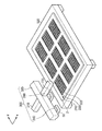
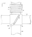
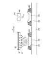
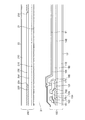
図1は、本発明の実施形態1によるインクジェットプリンティングシステムの斜視図であり、図2は本発明の実施形態1によるインクジェットプリンティングシステムのヘッドユニット、乾燥ユニット及び移送装置の底面図である、図3は本発明の実施形態1によるインクジェットプリンティングシステムのインクジェットヘッドを利用してインキをプリンティングする方法を概略的に説明した図であり、図4は本発明の実施形態1によるインクジェットプリンティングシステムの乾燥ユニットを利用して滴下されたインキを乾燥させる状態を示した図である。 FIG. 1 is a perspective view of an inkjet printing system according to Embodiment 1 of the present invention, and FIG. 2 is a bottom view of a head unit, a drying unit, and a transfer device of the inkjet printing system according to Embodiment 1 of the present invention. FIG. 4 is a diagram schematically illustrating a method of printing ink using the inkjet head of the inkjet printing system according to the first embodiment of the present invention, and FIG. 4 illustrates a drying unit of the inkjet printing system according to the first embodiment of the present invention. It is the figure which showed the state which dries the ink dripped using.
図1乃至図4に示したように、インクジェットプリンティングシステムは、母基板2が搭載されるステージ500、ステージ500上に所定間隔に離隔して位置するヘッドユニット700、ヘッドユニット700と所定間隔に離隔して位置している乾燥ユニット50、そしてヘッドユニット700及び乾燥ユニット50を所定位置に移動させる移送装置300を含む。
As shown in FIGS. 1 to 4, the inkjet printing system includes a
ステージ500は、母基板2を支持できるように母基板2より大きいのが好ましく、母基板2は液晶表示装置の色フィルター表示板、有機発光表示装置の薄膜トランジスタ表示板などの支持板として用いられる複数のサブ基板210で構成される。
図1には液晶表示装置の色フィルター表示板を形成するための母基板2が示されていて、各々のサブ基板210上には複数の開口部225を有する遮光部材220が形成されている。
The
FIG. 1 shows a
ヘッドユニット700は、インクジェットヘッド400、インクジェットヘッド400を移送装置300に付着させる連結部710(図示せず)を含む。インクジェットヘッド400は長い棒状を有し、その底面に複数のノズル410が設置されている。ノズル410を通してインキ5が基板上に滴下される。インクジェットヘッド400は、Y方向に対して所定角度(θ)で傾いている。つまり、インクジェットヘッド400において互いに隣接したノズル410間の距離であるノズルピッチ(D)とプリンティングされる画素間の距離である画素ピッチ(P)が異なるため、インクジェットヘッド400を所定角度(θ)だけ回転させることによって、ノズル410から滴下されるインキ5の間の間隔を画素ピッチ(P)と一致させる。ここで、画素ピッチ(P)=ノズルピッチ(D)×cosθとなる。図2で、インクジェットヘッド400は一つだけ図示したが、複数個でもよい。
The
乾燥ユニット50は、ステージ500と所定間隔に離隔して上に設置されていて、ヘッドユニット700とY方向に所定間隔に離隔して設置されている。乾燥ユニット50は複数の真空孔51とヒーター52を含む。ヒーター52は板状に形成されてもよく、真空孔51と真空孔51との間に形成されてもよい。また、ヒーター52は、真空孔51に沿ってくねくねと曲って形成されても良い。サブ基板210上に滴下されたインキ5の溶媒を真空孔51を通して吸収し、真空引きダクトで一括排気することによってインキ5を乾燥させ、ヒーター52を利用して熱線を照射することによってインキ5を乾燥させる。また、乾燥ユニット50は、ヘッドユニット700の進行方向(X方向)と垂直方向(Y方向)に所定間隔に離隔して設置されている。
The drying
移送装置300は、ヘッドユニット700及び乾燥ユニット50をサブ基板210の上側で所定間隔に離して位置させ、ヘッドユニット700及び乾燥ユニット50をY方向に移送させるY方向移送部310、ヘッドユニット700及び乾燥ユニット50をX方向に移送させるX方向移送部320、そしてヘッドユニット700及び乾燥ユニット50を昇降させる昇降部330、340を含む。
The
このような構造を有するインクジェットプリンティングシステムを利用してサブ基板210上に色フィルターを形成する動作を説明する。
まず、インクジェットプリンティングシステムの移送装置300のXまたはY方向移送部320、310と昇降部330の動作によって、ヘッドユニット700は当該サブ基板210上に位置する。
An operation of forming a color filter on the sub-substrate 210 using the inkjet printing system having such a structure will be described.
First, the
次に、移送装置300のX方向移送部320とインクジェットヘッド400のノズル410を駆動させてヘッドユニット700をX方向に移動させながら、図3に示したように、一列(row)にインキ5を落とす。
次に、ヘッドユニット700をY方向に所定間隔に移動させてインキ5が落ちた列に隣接した列に位置させ、X方向にヘッドユニット700を移動させながら再びインキ5を落とす。この時、乾燥ユニット50は、ヘッドユニット700とY方向に所定間隔に離隔しているため、インキ5が既に落ちた列を追ってX方向に移動しながらインキ5を乾燥させる。真空孔51とヒーター52を同時に利用してインキ5を乾燥させることによって、より急速にインキ5を乾燥できる。
Next, while driving the
Next, the
また、ヘッドユニット700によるインキの滴下動作と略同時に乾燥ユニット50を利用してインキを乾燥でき、乾燥ユニット50を利用して乾燥時間及び乾燥条件を調節でき、色フィルター230のプロファイル及び厚さの均一性を向上できる。
また、インキ滴下後、速くインキを乾燥させることによって、インキから蒸発する少量の溶媒によるヘッドユニット700の汚染を防止できる。
Also, the ink can be dried using the drying
In addition, by drying the ink quickly after the ink is dropped, the
一方、このような実施形態1によるインクジェットプリンティングシステムによって製造される表示板は、液晶表示装置の色フィルター表示板または有機発光表示装置の薄膜トランジスタ表示板でもよい。つまり、本発明の実施形態1によるインクジェットプリンティングシステムによって、液晶表示装置の色フィルターまたは有機発光表示装置の有機発光部材を形成できる。このとき、インキは、色フィルター用インキまたは有機発光部材用インキを用いる。 Meanwhile, the display panel manufactured by the inkjet printing system according to the first embodiment may be a color filter display panel of a liquid crystal display device or a thin film transistor display panel of an organic light emitting display device. That is, the color filter of the liquid crystal display device or the organic light emitting member of the organic light emitting display device can be formed by the inkjet printing system according to the first embodiment of the present invention. At this time, the ink is a color filter ink or an organic light emitting member ink.
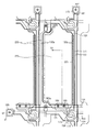
図5は本発明の一つの実施形態によるインクジェットプリンティングシステムで完成した液晶表示装置の配置図であり、図6は図5の液晶表示装置をVI-VI線に沿って切断した断面図である。
図5及び図6に示したように、液晶表示装置は下側の薄膜トランジスタ表示板100とこれと対向している上側の色フィルター表示板200、及びこれらの間に形成されて二つの表示板100、200の間に注入されている液晶層3で構成される。
FIG. 5 is a layout view of a liquid crystal display device completed by an inkjet printing system according to an embodiment of the present invention, and FIG. 6 is a cross-sectional view of the liquid crystal display device of FIG. 5 taken along line VI-VI.
As shown in FIGS. 5 and 6, the liquid crystal display device includes a lower thin film
まず、図5及び図6を参照して薄膜トランジスタ表示板100について詳細に説明する。
透明なガラスまたはプラスチックなどで形成された絶縁基板110上に複数のゲート線121及び複数の維持電極線131が形成されている。ゲート線121はゲート信号を伝達し、主に横方向に伸びている。各ゲート線121は上下に突出した複数のゲート電極124と他の層または外部駆動回路との接続のために面積が広い端部129を含む。維持電極線131は所定の電圧を印加されて、ゲート線121とほとんど並行に伸びた幹線とこれから分かれた複数対の第1及び第2維持電極133a、133bを含む。各々の維持電極線131は隣接した二つのゲート線121の間に位置し、幹線は二つのゲート線121のうちの下側に近い。
First, the thin film
A plurality of
ゲート線121及び維持電極線131上には窒化ケイ素(SiNx)または酸化ケイ素(SiOx)などで形成されたゲート絶縁膜140が形成されている。
ゲート絶縁膜140上には水素化非晶質シリコン(非晶質シリコンは略称a-Siに使う)または多結晶シリコンなどで形成された複数の線状半導体151が形成されている。線状半導体151は主に縦方向に伸びていて、ゲート電極124に向かって伸びた複数の突出部154を含む。線状半導体151は、ゲート線121及び維持電極線131付近で幅が広くなりこれらを広い幅で覆っている。
A
On the
半導体151上には複数の線状及び島型抵抗性接触部材161、165が形成されている。抵抗性接触部材161、165は、リンなどのn型不純物が高濃度にドーピングされているn+水素化非晶質シリコンなどの物質で形成されたり、シリサイドで形成できる。線状抵抗性接触部材161は複数の突出部163を有して、この突出部163と島型抵抗性接触部材165は対をなして半導体151の突出部154上に配置されている。
A plurality of linear and island-type
抵抗性接触部材161、165及びゲート絶縁膜140上には、複数のデータ線171と複数のドレーン電極175が形成されている。
データ線171はデータ信号を伝達し、主に縦方向に伸びてゲート線121と交差する。各データ線171は、また、維持電極線131と交差して隣接した維持電極133a、133b集合の間を走る。各データ線171は、ゲート電極124に向かって伸びた複数のソース電極173と他の層または外部駆動回路との接続のために面積が広い端部179を含む。
A plurality of
The
ドレーン電極175は、データ線171と分離されてゲート電極124を中心にソース電極173と対向する。各ドレーン電極175は広い一側端部と棒状である他側の端部を含む。広い端部は維持電極137と重なって、棒状端部は曲がったソース電極173で一部囲まれている。
一つのゲート電極124、一つのソース電極173及び一つのドレーン電極175は、半導体151の突出部154と共に一つの薄膜トランジスタ(TFT)をなし、薄膜トランジスタのチャンネルはソース電極173とドレーン電極175の間の突出部154に形成される。
The
One
抵抗性接触部材161、165は、その下の半導体151とその上のデータ線171及びドレーン電極175の間にだけ存在してこれらの間の接触抵抗を低くする。
データ線171、ドレーン電極175及び露出された半導体151部分上には保護膜180が形成されている。保護膜180は無機絶縁物または有機絶縁物などで形成され、その表面が平坦でもよい。
The
A
保護膜180にはデータ線171の端部179とドレーン電極175を各々露出する複数の接触孔182、185が形成されており、保護膜180とゲート絶縁膜140にはゲート線121の端部129を露出する複数の接触孔181、第1維持電極133aの固定端付近の維持電極線131一部を露出する複数の接触孔183a、そして第1維持電極133a自由端の突出部を露出する複数の接触孔183bが形成されている。
A plurality of
保護膜180上には複数の画素電極191、複数の連結橋83及び複数の接触補助部材81、82が形成されている。
画素電極191は、接触孔185を通してドレーン電極175と物理的・電気的に連結されており、ドレーン電極175からデータ電圧の印加を受ける。データ電圧が印加された画素電極191は、共通電圧を印加される他の表示板200の共通電極270と共に電場を生成することによって、二つの電極の間の液晶層3の液晶分子の方向を決定する。このように決定された液晶分子の方向によって液晶層を通過する光の偏光が変わる。画素電極191と共通電極270は、蓄電器(以下、“液晶蓄電器”という)を構成して薄膜トランジスタが遮断された後にも印加された電圧を維持する。
A plurality of
The
画素電極191及びこれと連結されたドレーン電極175は、維持電極133a、133bをはじめとする維持電極線131と重なる。画素電極191及びこれと電気的に連結されたドレーン電極175が維持電極線131と重なって形成する蓄電器を維持蓄電器として、維持蓄電器は液晶蓄電器の電圧維持能力を強化する。
接触補助部材81、82は、各々接触孔181、182を通してゲート線121の端部129及びデータ線171の端部179と連結される。接触補助部材81、82は、ゲート線121の端部129及びデータ線171の端部179と外部装置との接着性を補ってこれらを保護する。
The
The
連結橋83はゲート線121を横切って、ゲート線121を間に置いて反対方向に位置する接触孔183a、183bを通して、維持電極線131の露出された部分と維持電極133bの自由端の露出された端部に連結されている。維持電極133a、133bをはじめとする維持電極線131は、連結橋83と共にゲート線121やデータ線171または薄膜トランジスタの欠陥の修理に用いられる。
The
次に、色フィルター表示板200について図5及び図6を参照して説明する。
透明なガラスまたはプラスチックなどで形成された絶縁性のサブ基板210の下に遮光部材220が形成されている。遮光部材220はブラックマトリックスともいい、光漏れを防ぐ。遮光部材220は、画素電極191と対向して画素電極191とほとんど同じ形をする複数の開口部225を有し、画素電極191の間の光漏れを防止する。しかし、遮光部材220は、ゲート線121及びデータ線171に対応する部分と薄膜トランジスタに対応する部分で構成できる。このような遮光部材220は、インクジェットプリンティングシステムを利用した色フィルター表示板の製造工程時、色フィルター用インキを閉じ込める隔壁部材の役割を果たす。
Next, the color
A
遮光部材220の開口部225には、インクジェットプリンティングシステムによって形成された複数の色フィルター230が位置している。色フィルター230は遮光部材230に囲まれた領域内に殆んど存在し、画素電極191列に沿って縦方向に長く伸びてもよい。各色フィルター230は、赤色、緑色及び青色の三原色など基本色のうちの一つを表示できる。
A plurality of
色フィルター230及び遮光部材220の下には、蓋膜250が形成されている。蓋膜250は有機絶縁物で形成できて、色フィルター230が露出されることを防止して平坦面を提供する。蓋膜250は省略できる。
蓋膜250上には共通電極270が形成されている。共通電極270はITO、IZOなどの透明な導電体などで形成される。
A
A
表示板100、200の内側面には、配向膜11、21が塗布されていて、これらは水平配向膜または垂直配向膜でもよい。表示板100、200の外側面には偏光子12、22が備えられているが、二つの偏光子12、22の偏光軸は直交し、そのうち一つの偏光軸はゲート線121に対して平行であるのが望ましい。反射型液晶表示装置の場合には二つの偏光子12、22のうちの一つが省略できる。
The
図5及び図6に示した色フィルター表示板を製造する方法について詳細に説明する。
まず、透明なガラス等で形成された絶縁サブ基板210の下に、クロムなどの金属膜を真空蒸着などの方法で形成して写真エッチングして複数の開口部225を有する遮光部材220を形成する。また、遮光部材220は絶縁サブ基板210の下に高分子樹脂溶液を積層してスピンコーティング処理して写真エッチングして形成でき、慣用的な多様な方法で形成できる。
A method for manufacturing the color filter display panel shown in FIGS. 5 and 6 will be described in detail.
First, a
次に、遮光部材20の開口部225内にインクジェットプリンティングシステムを利用して色フィルター230を形成する。つまり、ヘッドユニット700を移動させながらノズル410を通して開口部225に赤色フィルター、緑色フィルターまたは青色フィルターに該当する液状の顔料ペースト、つまり、インキ5を滴下して開口部225を詰め込むことによって、色フィルター230を形成する。そして、ヘッドユニット700に隣接した乾燥ユニット50を滴下されたインキ上に直ちに位置させて、真空及び熱を利用してインキを乾燥させて色フィルター230を完成する。従って、色フィルター230のプロファイル及び厚さが均一となる。
Next, the
次に、色フィルター230及び遮光部材220の上(薄膜トランジスタ表示板100に近づく方向)に有機絶縁物に蓋膜250を形成する。次に、蓋膜250の下にITO、IZOなどの透明な導電体などに共通電極270を形成する。
一方、本発明の実施形態1によるインクジェットプリンティングシステムを利用して完成した有機発光表示装置について説明する。
Next, a
Meanwhile, an organic light emitting display device completed using the inkjet printing system according to the first embodiment of the present invention will be described.
まず、本発明の実施形態1によるインクジェットプリンティングシステムを利用して完成した有機発光表示装置の等価回路について図7を参照して詳細に説明する。図7は本発明の実施形態1による有機発光表示装置の等価回路図である。
図7を参照すると、本発明の実施形態1によるインクジェットプリンティングシステムを利用して完成した有機発光表示装置は、複数の信号線121、171、172とこれらに連結されて行列状に配列された複数の画素(PX)を含む。
First, an equivalent circuit of the organic light emitting display device completed using the inkjet printing system according to the first embodiment of the present invention will be described in detail with reference to FIG. FIG. 7 is an equivalent circuit diagram of the OLED display according to the first exemplary embodiment of the present invention.
Referring to FIG. 7, the OLED display completed using the inkjet printing system according to the first embodiment of the present invention includes a plurality of
信号線は、ゲート信号(または走査信号)を伝達する複数のゲート線121、データ信号を伝達する複数のデータ線171及び駆動電圧を伝達する複数の駆動電圧線172を含む。ゲート線121は行方向に伸びて互いに平行し、データ線171と駆動電圧線172は列方向に伸びて互いに平行する。
各画素(PX)はスイッチングトランジスタ(Qs)、駆動トランジスタ(Qd)、維持蓄電器(Cst)及び有機発光ダイオード(LD)を含む。
The signal lines include a plurality of
Each pixel (PX) includes a switching transistor (Qs), a driving transistor (Qd), a storage capacitor (Cst), and an organic light emitting diode (LD).
スイッチングトランジスタ(Qs)は、制御端子、入力端子、及び出力端子を有するが、制御端子はゲート線121に連結されており、入力端子はデータ線171に連結されており、出力端子は駆動トランジスタ(Qd)に連結されている。スイッチングトランジスタ(Qs)は、ゲート線121に印加される走査信号に応答してデータ線171に印加されるデータ信号を駆動トランジスタ(Qd)に伝達する。
The switching transistor (Qs) has a control terminal, an input terminal, and an output terminal. The control terminal is connected to the
駆動トランジスタ(Qd)も、制御端子、入力端子及び出力端子を有するが、制御端子はスイッチングトランジスタ(Qs)に連結されており、入力端子は駆動電圧線172に連結されており、出力端子は有機発光ダイオード(LD)に連結されている。駆動トランジスタ(Qd)は、制御端子と出力端子の間にかかる電圧によってその値が変わる出力電流(ILD)を流す。
The drive transistor (Qd) also has a control terminal, an input terminal, and an output terminal, but the control terminal is connected to the switching transistor (Qs), the input terminal is connected to the
蓄電器(Cst)は、駆動トランジスタ(Qd)の制御端子と入力端子の間に連結されている。前記蓄電器(Cst)は、駆動トランジスタ(Qd)の制御端子に印加されるデータ信号を充電してスイッチングトランジスタ(Qs)が遮断された後にもこれを維持する。
有機発光ダイオード(LD)は、駆動トランジスタ(Qd)の出力端子に連結されているアノードと共通電圧(Vss)に連結されているカソードを有する。有機発光ダイオード(LD)は、駆動トランジスタ(Qd)の出力電流(ILD)によって強さを異ならせて発光することによって映像を表示する。
The battery (Cst) is connected between the control terminal and the input terminal of the drive transistor (Qd). The capacitor (Cst) charges the data signal applied to the control terminal of the driving transistor (Qd) and maintains it even after the switching transistor (Qs) is cut off.
The organic light emitting diode (LD) has an anode connected to the output terminal of the driving transistor (Qd) and a cathode connected to a common voltage (Vss). The organic light emitting diode (LD) displays an image by emitting light with different intensity depending on the output current (ILD) of the driving transistor (Qd).
スイッチングトランジスタ(Qs)及び駆動トランジスタ(Qd)は、n-チャンネル電界効果トランジスタ(FET)である。しかし、スイッチングトランジスタ(Qs)と駆動トランジスタ(Qd)のうちの少なくとも一つは、p-チャンネル電界効果トランジスタでもよい。また、トランジスタ(Qs、Qd)、蓄電器(Cst)及び有機発光ダイオード(LD)の連結関係が変わることもありうる。 The switching transistor (Qs) and the driving transistor (Qd) are n-channel field effect transistors (FETs). However, at least one of the switching transistor (Qs) and the driving transistor (Qd) may be a p-channel field effect transistor. In addition, the connection relationship of the transistors (Qs, Qd), the capacitor (Cst), and the organic light emitting diode (LD) may change.
以下、図7に示した有機発光表示装置用表示板の構造について図8及び図9を参照して詳細に説明する。
図8は、本発明の実施形態1によるインクジェットプリンティングシステムを利用して完成した有機発光表示装置の有機発光表示板の配置図であり、図9は図8の有機発光表示板をIX-IX線に沿って切断して示した断面図である。
Hereinafter, the structure of the OLED display panel shown in FIG. 7 will be described in detail with reference to FIGS.
FIG. 8 is a layout view of an organic light emitting display panel of the organic light emitting display device completed using the inkjet printing system according to the first embodiment of the present invention, and FIG. 9 illustrates the organic light emitting display panel of FIG. It is sectional drawing cut | disconnected and shown along.
図8及び図9に示したように、透明なガラスまたはプラスチックなどで形成された絶縁基板110上に第1制御電極124aを含む複数のゲート線121及び複数の第2制御電極124bを含む複数のゲート導電体が形成されている。
ゲート線121は、ゲート信号を伝達して主に横方向に伸びている。各ゲート線121は、他の層または外部駆動回路との接続のために面積が広い端部129を含み、第1制御電極124aはゲート線121から上に伸びている。ゲート信号を生成するゲート駆動回路(図示せず)が基板110上に集積されている場合、ゲート線121が伸びてゲート駆動回路と直接連結される。
8 and 9, a plurality of
The
第2制御電極124bはゲート線121と分離されていて、下方向に伸びるが右方に少し方向を変えて上方に長く伸びた維持電極127を含む。
ゲート導電体121、124bは、アルミニウム(Al)やアルミニウム合金などアルミニウム系金属、銀(Ag)や銀合金など銀系金属、銅(Cu)や銅合金など銅系金属、モリブデン(Mo)やモリブデン合金などモリブデン系金属、クロム(Cr)、タンタル(Ta)及びチタン(Ti)などで形成できる。
The
The
ゲート導電体121、124b上には、窒化ケイ素(SiNx)または酸化ケイ素(SiOx)などで構成されたゲート絶縁膜140が形成されている。
ゲート絶縁膜140上には水素化非晶質シリコン(非晶質シリコンは略称a-Siという)または多結晶シリコンなどで構成された複数の第1及び第2島型半導体154a、154bが形成されている。第1及び第2半導体154a、154bは、各々第1及び第2制御電極124a、124b上に位置する。
A
A plurality of first and second
第1及び第2半導体154a、154bの上には各々複数対の第1抵抗性接触部材163a、165aと複数対の第2抵抗性接触部材163b、165bが形成されている。抵抗性接触部材163a、163b、165a、165bは、島状であり、リンなどのn型不純物が高濃度にドーピングされているn+水素化非晶質シリコンなどの物質で構成されたシリサイドで形成できる。第1抵抗性接触部材163a、165aは、対をなして第1半導体154a上に配置されていて、第2抵抗性接触部材163b、165bも、対をなして第2半導体154b上に配置されている。
A plurality of pairs of first resistive contact members 163a and 165a and a plurality of pairs of second
抵抗性接触部材163a、163b、165a、165b及びゲート絶縁膜140上には、複数のデータ線171と複数の駆動電圧線172と複数の第1及び第2出力電極175a、175bを含む複数のデータ導電体が形成されている。
データ線171は、データ信号を伝達して主に縦方向に伸びてゲート線121と交差する。各データ線171は、第1制御電極124aに向かって伸びた複数の第1入力電極173aと他の層または外部駆動回路との接続のために面積が広い端部179を含む。
A plurality of data including a plurality of
The
駆動電圧線172は、駆動電圧を伝達して主に縦方向に伸びてゲート線121と交差する。各駆動電圧線172は、第2制御電極124bに向かって伸びた複数の第2入力電極173bを含む。駆動電圧線172は、維持電極127と重なって互いに連結される。
第1及び第2出力電極175a、175bは、互いに分離されていてデータ線171及び駆動電圧線172とも分離されている。第1入力電極173aと第1出力電極175aは、第1制御電極124aを中心に互いに対向し、第2入力電極173bと第2出力電極175bは第2制御電極124bを中心に互いに対向する。
The
The first and
データ導電体171、172、175a、175bは、モリブデン、クロム、タンタル及びチタンなど耐火性金属またはこれらの合金で形成されるのが望ましく、耐火性金属膜(図示せず)と低抵抗導電膜(図示せず)を含む多重膜構造を有することができる。
抵抗性接触部材163a、163b、165a、165bは、その下の半導体154a、154bとその上のデータ導電体171、172、175a、175bの間にだけ存在して接触抵抗を低くする。半導体154a、154bには入力電極173a、173bと出力電極175a、175bの間をはじめとして、データ導電体171、172、175a、175bで覆わずに露出される部分がある。
The
データ導電体171、172、175a、175bと露出された半導体154a、154b部分の上には保護膜180が形成されている。保護膜180は、窒化ケイ素や酸化ケイ素などの無機絶縁物、有機絶縁物、低誘電率絶縁物などで形成される。また、保護膜180は半導体154の露出された部分を保護しながらも有機膜の長所を生かすことができるように、下部無機膜と上部有機膜の二重膜構造で構成できる。
A
保護膜180には、データ線171の端部179と第1及び第2出力電極175bを各々露出する複数の接触孔182、185a、185bが形成されており、保護膜180とゲート絶縁膜140には、ゲート線121の端部129と第2入力電極124bを各々露出する複数の接触孔181、184が形成されている。
保護膜180上には複数の画素電極191、複数の連結部材85及び複数の接触補助部材81、82が形成されている。これらはITOまたはIZOなどの透明な導電物質やアルミニウム、銀またはその合金などの反射性金属で形成できる。
The
A plurality of
画素電極191は、接触孔185bを通して第2出力電極175bと物理的・電気的に連結されており、連結部材85は、接触孔184、185aを通して第2制御電極124b及び第1出力電極175aと連結されている。
接触補助部材81、82は、各々接触孔181、182を通してゲート線121の端部129及びデータ線171の端部179と連結される。接触補助部材81、82は、ゲート線121の端部129及びデータ線171の端部179と外部装置との接着性を補ってこれらを保護する。
The
The
保護膜180上には隔壁361が形成されている。隔壁361は画素電極191周縁を堤防のように囲んで開口部365を定義し、有機絶縁物または無機絶縁物で形成される。隔壁361はまた、黒色顔料を含む感光剤で形成できるが、この場合、隔壁361は遮光部材の役割を果たし、その形成工程が簡単である。
隔壁361が定義する画素電極191上の開口部365内には本発明の実施形態1であるインクジェットプリンティングシステムによって形成された有機発光部材370がある。有機発光部材370は赤色、緑色、青色の三原色など基本色のうちのいずれか一つの光を固有に発光する有機物質で形成される。有機発光表示装置は有機発光部材370が出す基本色発光の空間的な合計で所望の映像を表示する。
A
In the
有機発光部材370は発光する発光層(図示せず)の他に発光層の発光効率を向上するための付帯層(図示せず)を含む多層構造を有することができる。付帯層には電子と正孔の均衡を取るための電子輸送層(図示せず)及び正孔輸送層(図示せず)と電子と正孔の注入を強化するための電子注入層(図示せず)及び正孔注入層(図示せず)などがある。
有機発光部材370上には共通電極270が形成されている。共通電極270は共通電圧(Vss)を印加して、カルシウム(Ca)、バリウム(Ba)、マグネシウム(Mg)、アルミニウム、銀などを含む反射性金属またはITOまたはIZOなどの透明な導電物質で形成される。
The organic
A
このような有機発光表示装置において、ゲート線121に連結されている第1制御電極124a、データ線171に連結されている第1入力電極173a及び第1出力電極175aは、第1半導体154aと共にスイッチング薄膜トランジスタ(Qs)をなし、スイッチング薄膜トランジスタ(Qs)のチャンネルは第1入力電極173aと第1出力電極175aの間の第1半導体154aに形成される。第1出力電極175aに連結されている第2制御電極124b、駆動電圧線172に連結されている第2入力電極173b及び画素電極191に連結されている第2出力電極175bは、第2半導体154bと共に駆動薄膜トランジスタ(Qd)をなし、駆動薄膜トランジスタ(Qd)のチャンネルは、第2入力電極173bと第2出力電極175bの間の第2半導体154bに形成される。画素電極191、有機発光部材370及び共通電極270は、有機発光ダイオード(LD)をなし、画素電極191がアノード、共通電極270がカソードになったり、逆に画素電極191がカソード、共通電極270がアノードとなる。互いに重なる維持電極127と駆動電圧線172は維持蓄電器(Cst)を構成する。
In the organic light emitting display device, the
このような有機発光表示装置は、基板110の上方または下方に光を発光して映像を表示する。不透明な画素電極191と透明な共通電極270は、基板110の上側方向に映像を表示する前面発光方式の有機発光表示装置に適用して、透明な画素電極191と不透明な共通電極270は、基板110の下方向に映像を表示する背面発光方式の有機発光表示装置に適用する。
Such an organic light emitting display displays light by emitting light above or below the
一方、本発明の実施形態1では非晶質シリコンで構成される半導体154a、154bを有する有機発光表示装置用表示板について説明したが、本発明の内容は多結晶シリコンで構成される半導体を有する有機発光表示装置用表示板にも適用できる。
以上で本発明の望ましい実施形態について詳細に説明したが、当該技術分野における通常の知識を有する者ならばこれから多様な変形及び均等な他の実施形態が可能であるという点を理解できる。従って、本発明の権利範囲はこれに限定されることなく、特許請求の範囲で定義している本発明の基本概念を利用した当業者の多様な変形及び改良形態も、本発明の権利範囲に属する。
Meanwhile, in the first embodiment of the present invention, the display panel for an organic light emitting display device having the
Although the preferred embodiments of the present invention have been described in detail above, those skilled in the art can understand that various modifications and other equivalent embodiments are possible. Therefore, the scope of right of the present invention is not limited to this, and various modifications and improvements of those skilled in the art using the basic concept of the present invention defined in the claims are also within the scope of the present invention. Belongs.
2 母基板
50 乾燥ユニット
51 真空孔
52 ヒーター
210 サブ基板
300 移送装置
310 Y方向移送部
320 X方向移送部
330、340 昇降部
400 ヘッドユニット
410 ノズル
500 ステージ
700 ヘッドユニット
2
Claims (17)
前記基板上にインキを滴下するヘッドユニット、
前記基板上に滴下されたインキを乾燥させる乾燥ユニット、そして
前記ヘッドユニット及び乾燥ユニットを所定位置に移動させる移送装置
を含み、
前記乾燥ユニットには真空孔が形成されていることを特徴とするインクジェットプリンティングシステム。 The stage on which the board is mounted,
A head unit for dropping ink on the substrate;
A drying unit that dries ink dropped on the substrate, and a transfer device that moves the head unit and the drying unit to predetermined positions.
An inkjet printing system, wherein a vacuum hole is formed in the drying unit.
前記ヘッドユニットを移動させて前記インクジェットヘッドのノズルを通して基板上にインキを滴下する段階、そして
前記滴下されたインキを前記ヘッドユニットに隣接した乾燥ユニットを利用して乾燥させる段階
を含み、
前記乾燥ユニットには真空孔が形成されることを特徴とする製造方法。 Positioning a head unit including an inkjet head having a plurality of nozzles on a substrate;
Moving the head unit to drop ink onto a substrate through a nozzle of the inkjet head; and drying the dropped ink using a drying unit adjacent to the head unit.
A manufacturing method, wherein a vacuum hole is formed in the drying unit.
Applications Claiming Priority (1)
| Application Number | Priority Date | Filing Date | Title |
|---|---|---|---|
| KR1020060001239A KR20070073394A (en) | 2006-01-05 | 2006-01-05 | Ink jet printing system and manufacturing method of display device using the same |
Publications (2)
| Publication Number | Publication Date |
|---|---|
| JP2007183641A true JP2007183641A (en) | 2007-07-19 |
| JP2007183641A5 JP2007183641A5 (en) | 2009-09-10 |
Family
ID=38223909
Family Applications (1)
| Application Number | Title | Priority Date | Filing Date |
|---|---|---|---|
| JP2006354149A Abandoned JP2007183641A (en) | 2006-01-05 | 2006-12-28 | Ink jet printing system and manufacturing method using the same |
Country Status (4)
| Country | Link |
|---|---|
| US (1) | US20070153075A1 (en) |
| JP (1) | JP2007183641A (en) |
| KR (1) | KR20070073394A (en) |
| CN (1) | CN1994741A (en) |
Cited By (2)
| Publication number | Priority date | Publication date | Assignee | Title |
|---|---|---|---|---|
| WO2011155808A2 (en) * | 2010-06-11 | 2011-12-15 | 한국기계연구원 | Apparatus and method for printing process simulation |
| JP2013214514A (en) * | 2012-03-30 | 2013-10-17 | Semes Co Ltd | Substrate processing apparatus and substrate processing method |
Families Citing this family (19)
| Publication number | Priority date | Publication date | Assignee | Title |
|---|---|---|---|---|
| US9011967B2 (en) * | 2009-06-04 | 2015-04-21 | E I Du Pont De Nemours And Company | Multicolor electronic devices and processes of forming the same by printing |
| US8890187B2 (en) * | 2010-04-16 | 2014-11-18 | Semiconductor Energy Laboratory Co., Ltd. | Light-emitting device with an insulating partition |
| US8602532B2 (en) | 2011-04-30 | 2013-12-10 | Hewlett-Packard Development Company, L.P. | Electrowetting mechanism for fluid-application device |
| KR101350948B1 (en) * | 2011-09-30 | 2014-01-14 | 세메스 주식회사 | Apparatus and method for treating substrate |
| US9824410B1 (en) | 2013-04-29 | 2017-11-21 | Grubhub Holdings Inc. | System, method and apparatus for assessing the accuracy of estimated food delivery time |
| KR102131118B1 (en) | 2013-07-04 | 2020-07-08 | 삼성디스플레이 주식회사 | Mask for forming semiconductor pattern and apparatus for forming semiconductor pattern having the same and method for manufacturing semiconductor device using the same |
| CN104260554B (en) | 2014-09-24 | 2016-03-30 | 京东方科技集团股份有限公司 | The preparation method of inkjet printing methods and equipment, display base plate |
| CN106915158B (en) * | 2016-06-01 | 2019-03-12 | 广东聚华印刷显示技术有限公司 | Printing system and method |
| CN109216573A (en) * | 2017-06-30 | 2019-01-15 | 京东方科技集团股份有限公司 | The preparation method of cold plate and preparation method thereof, drying equipment, oled panel |
| CN110091592B (en) * | 2018-04-23 | 2020-07-10 | 广东聚华印刷显示技术有限公司 | Ink jet printing method, apparatus, system, computer device and storage medium |
| CN109817842B (en) * | 2019-01-16 | 2021-10-01 | 京东方科技集团股份有限公司 | Vacuum drying device and preparation method of display substrate |
| CN109830614B (en) * | 2019-02-19 | 2020-11-13 | 京东方科技集团股份有限公司 | Flexible display substrate and flexible display device |
| CN109720105A (en) * | 2019-03-13 | 2019-05-07 | 苏州星烁纳米科技有限公司 | For printing the spray head of quantum dispensing liquid |
| CN109720104A (en) * | 2019-03-13 | 2019-05-07 | 苏州星烁纳米科技有限公司 | It is used to prepare the ink jet printing device of quantum dot colour filter |
| CN110116559A (en) * | 2019-04-23 | 2019-08-13 | 深圳市华星光电半导体显示技术有限公司 | Vacuum dryer |
| CN110588186B (en) * | 2019-08-07 | 2020-07-10 | 华中科技大学 | Manufacturing system and method of ink-jet printing flexible display device |
| KR102643857B1 (en) | 2021-11-02 | 2024-03-07 | 한국생산기술연구원 | Dispersion flow path apparatus and Vacuum drying apparatus with the same |
| KR20230066880A (en) | 2021-11-08 | 2023-05-16 | 한국생산기술연구원 | Vacuum drying apparatus with substrate heater means and vapor dispersion cooling plate |
| CN115157876B (en) * | 2022-06-24 | 2023-09-29 | 昆山国显光电有限公司 | Printing and drying device and preparation method of display panel |
Family Cites Families (4)
| Publication number | Priority date | Publication date | Assignee | Title |
|---|---|---|---|---|
| US6394596B1 (en) * | 1999-10-05 | 2002-05-28 | Hewlett-Packard Company | Belt-type media support for a printer |
| US6505928B1 (en) * | 2000-05-15 | 2003-01-14 | Digital Printing Systems, Llc | Methods and apparatus for ink jet printing with forced air drying |
| JP3880289B2 (en) * | 2000-05-23 | 2007-02-14 | キヤノン株式会社 | Head unit, color filter manufacturing apparatus using the head unit, color filter manufacturing method, liquid crystal panel manufacturing method including color filter, and information processing apparatus manufacturing method including liquid crystal panel |
| US7368145B2 (en) * | 2002-09-19 | 2008-05-06 | Dai Nippon Printing Co., Ltd. | Method and apparatus for manufacturing organic EL display and color filter by ink jet method |
-
2006
- 2006-01-05 KR KR1020060001239A patent/KR20070073394A/en not_active Application Discontinuation
- 2006-11-30 US US11/565,248 patent/US20070153075A1/en not_active Abandoned
- 2006-12-28 JP JP2006354149A patent/JP2007183641A/en not_active Abandoned
-
2007
- 2007-01-05 CN CNA2007100005058A patent/CN1994741A/en active Pending
Cited By (4)
| Publication number | Priority date | Publication date | Assignee | Title |
|---|---|---|---|---|
| WO2011155808A2 (en) * | 2010-06-11 | 2011-12-15 | 한국기계연구원 | Apparatus and method for printing process simulation |
| WO2011155808A3 (en) * | 2010-06-11 | 2012-04-19 | 한국기계연구원 | Apparatus and method for printing process simulation |
| JP2013214514A (en) * | 2012-03-30 | 2013-10-17 | Semes Co Ltd | Substrate processing apparatus and substrate processing method |
| CN103357549A (en) * | 2012-03-30 | 2013-10-23 | 细美事有限公司 | Substrate processing device and substrate processing method |
Also Published As
| Publication number | Publication date |
|---|---|
| US20070153075A1 (en) | 2007-07-05 |
| KR20070073394A (en) | 2007-07-10 |
| CN1994741A (en) | 2007-07-11 |
Similar Documents
| Publication | Publication Date | Title |
|---|---|---|
| JP2007183641A (en) | Ink jet printing system and manufacturing method using the same | |
| JP4366988B2 (en) | Organic EL device and electronic device | |
| US7718476B2 (en) | Display apparatus and fabricating method thereof | |
| JP2007183627A (en) | Ink jet printing system and manufacturing method of display apparatus using the same | |
| KR101957838B1 (en) | Organec light emitting diode display device and method of manufacturing the same | |
| US7709838B2 (en) | Thin film transistor array panel | |
| JP2009038007A (en) | Organic electroluminescent display device | |
| JP2007156494A (en) | Display and manufacturing method thereof | |
| JP3580308B2 (en) | Device manufacturing method, device and electronic apparatus | |
| JP2006085170A (en) | Panel for display device and manufacturing method thereof | |
| JP2002366057A (en) | Display device | |
| JP5126168B2 (en) | Organic EL device and electronic device | |
| US20070153051A1 (en) | Manufacturing flat panel displays with inkjet printing systems | |
| KR101197048B1 (en) | Ink jet printing system | |
| JP2009004537A (en) | Organic device and its manufacturing method | |
| KR20060098305A (en) | Head unit for ink jet printing system | |
| US8268681B2 (en) | Display substrate and method of manufacturing the same | |
| JP2005085877A (en) | Method of manufacturing device, device, and electronic apparatus | |
| JP4470385B2 (en) | Electro-optical device, method of manufacturing electro-optical device, and electronic apparatus | |
| KR20060025101A (en) | Panel for a display device and method for manufacturing the same | |
| JP2006350329A (en) | Method for manufacturing display device | |
| CN108878536B (en) | Thin film transistor, manufacturing method of thin film transistor array substrate and display device | |
| JP3858810B2 (en) | Method for manufacturing light emitting device | |
| KR100553744B1 (en) | Flat panel display with TFT | |
| JP2010287628A (en) | Transistor substrate, and method of manufacturing the transistor substrate |
Legal Events
| Date | Code | Title | Description |
|---|---|---|---|
| A521 | Request for written amendment filed |
Free format text: JAPANESE INTERMEDIATE CODE: A523 Effective date: 20090727 |
|
| A621 | Written request for application examination |
Free format text: JAPANESE INTERMEDIATE CODE: A621 Effective date: 20090727 |
|
| A521 | Request for written amendment filed |
Free format text: JAPANESE INTERMEDIATE CODE: A523 Effective date: 20100705 |
|
| A762 | Written abandonment of application |
Free format text: JAPANESE INTERMEDIATE CODE: A762 Effective date: 20100709 |