JP2007166326A - Frequency modulator unit, and fm transmitter circuit using the same - Google Patents
Frequency modulator unit, and fm transmitter circuit using the same Download PDFInfo
- Publication number
- JP2007166326A JP2007166326A JP2005360968A JP2005360968A JP2007166326A JP 2007166326 A JP2007166326 A JP 2007166326A JP 2005360968 A JP2005360968 A JP 2005360968A JP 2005360968 A JP2005360968 A JP 2005360968A JP 2007166326 A JP2007166326 A JP 2007166326A
- Authority
- JP
- Japan
- Prior art keywords
- signal
- output
- frequency
- frequency modulator
- resistor
- Prior art date
- Legal status (The legal status is an assumption and is not a legal conclusion. Google has not performed a legal analysis and makes no representation as to the accuracy of the status listed.)
- Pending
Links
- 239000002131 composite material Substances 0.000 claims description 10
- 230000005236 sound signal Effects 0.000 claims description 10
- 239000004065 semiconductor Substances 0.000 claims description 5
- 239000000758 substrate Substances 0.000 claims description 5
- 239000003990 capacitor Substances 0.000 description 17
- 230000008878 coupling Effects 0.000 description 7
- 238000010168 coupling process Methods 0.000 description 7
- 238000005859 coupling reaction Methods 0.000 description 7
- 238000010586 diagram Methods 0.000 description 4
- 230000006870 function Effects 0.000 description 4
- 230000002238 attenuated effect Effects 0.000 description 3
- 239000000470 constituent Substances 0.000 description 3
- 238000000034 method Methods 0.000 description 3
- 230000014509 gene expression Effects 0.000 description 2
- 238000012986 modification Methods 0.000 description 2
- 230000004048 modification Effects 0.000 description 2
- 230000005540 biological transmission Effects 0.000 description 1
- 230000010354 integration Effects 0.000 description 1
- 230000008569 process Effects 0.000 description 1
- 238000005549 size reduction Methods 0.000 description 1
Images

Landscapes
- Stabilization Of Oscillater, Synchronisation, Frequency Synthesizers (AREA)
- Transmitters (AREA)
Abstract
Description
本発明は、PLL(Phase Locked Loop)を利用した直接変調型の周波数変調器に関する。 The present invention relates to a direct modulation type frequency modulator using a PLL (Phase Locked Loop).
FM放送や、車載用オーディオにおいて、送信すべきオーディオ信号(変調信号)にもとづいて、周波数変調された被変調信号を生成する周波数変調器が用いられている。たとえば、特許文献1には、電圧制御発振器(以下、VCOという)、分周器、位相比較器、ループフィルタを用いてPLLを構成し、VCOの入力信号に変調信号であるオーディオ信号を重畳する直接変調型の周波数変調器が開示されている。
In FM broadcasting and in-vehicle audio, a frequency modulator that generates a modulated signal subjected to frequency modulation based on an audio signal (modulated signal) to be transmitted is used. For example, in
特許文献1に開示されるように、従来の直列変調型の周波数変調器においては、ループフィルタの出力端子と、VCOの入力端子の間に、カップリングキャパシタや、加算用の抵抗を用いて変調信号をカップリングする手法がとられていた。
しかしながら、従来においては、カップリングキャパシタや抵抗を用いて、変調信号を高周波信号に重畳するため、PLLのループフィルタのインピーダンスが、変調信号である入力信号に影響を与えるという問題があった。変調信号がループフィルタに影響を受けると、変調信号の高域が減衰するため、たとえばオーディオ信号を変調するような場合には、信号に歪みが発生する。また、ループフィルタから出力される信号が、変調信号を生成する回路側にリークする場合があった。 However, conventionally, since the modulation signal is superimposed on the high-frequency signal using a coupling capacitor or a resistor, there is a problem that the impedance of the PLL loop filter affects the input signal that is the modulation signal. When the modulation signal is affected by the loop filter, the high frequency band of the modulation signal is attenuated. For example, when the audio signal is modulated, the signal is distorted. In addition, the signal output from the loop filter may leak to the circuit side that generates the modulation signal.
本発明はこうした課題に鑑みてなされたものであり、その目的は、PLLのループフィルタが変調信号におよぼす影響を抑えることができる周波数変調器の提供にある。 The present invention has been made in view of these problems, and an object thereof is to provide a frequency modulator capable of suppressing the influence of a PLL loop filter on a modulation signal.
発明のある態様の周波数変調器は、反転入力端子に第1抵抗を介して入力信号が入力された演算増幅器と、演算増幅器の出力端子と反転入力端子間の帰還経路に設けられた第2抵抗と、演算増幅器の出力信号が入力された電圧制御発振器と、電圧制御発振器の出力信号を分周する分周器と、分周器の出力信号を、基準クロック信号と比較し、位相差に応じた電圧を出力する位相比較器と、位相比較器の出力電圧の高周波成分を除去し、演算増幅器の非反転入力端子へと出力するフィルタと、を備える。 A frequency modulator according to an aspect of the invention includes an operational amplifier in which an input signal is input to an inverting input terminal via a first resistor, and a second resistor provided in a feedback path between the output terminal and the inverting input terminal of the operational amplifier. And the voltage controlled oscillator to which the output signal of the operational amplifier is input, the frequency divider that divides the output signal of the voltage controlled oscillator, and the output signal of the frequency divider is compared with the reference clock signal, and according to the phase difference And a filter that removes a high-frequency component of the output voltage of the phase comparator and outputs it to the non-inverting input terminal of the operational amplifier.
この態様において、第1抵抗、第2抵抗および演算増幅器は、入力信号に対しては、反転アンプとして機能し、フィルタの出力信号に対しては、非反転アンプとして機能する。その結果、演算増幅器によって、入力信号とフィルタの出力信号が重畳され、電圧制御発振器に入力される。この態様によれば、演算増幅器の入力インピーダンスは高いため、フィルタのインピーダンスが、入力信号が入力される入力端子側の回路に及ぼす影響を低減することができる。 In this aspect, the first resistor, the second resistor, and the operational amplifier function as an inverting amplifier for the input signal, and function as a non-inverting amplifier for the output signal of the filter. As a result, the input signal and the output signal of the filter are superimposed by the operational amplifier and input to the voltage controlled oscillator. According to this aspect, since the input impedance of the operational amplifier is high, the influence of the impedance of the filter on the circuit on the input terminal side to which the input signal is input can be reduced.
第1抵抗の抵抗値を第2抵抗の抵抗値より高く設定してもよい。この場合、入力信号を減衰させる一方で、ループゲインを低く設定することができる。 The resistance value of the first resistor may be set higher than the resistance value of the second resistor. In this case, the loop gain can be set low while the input signal is attenuated.
第1、第2抵抗の少なくとも一方は、可変抵抗であってもよい。この場合、電圧制御発振器の特性などに応じて、ループゲインや入力信号の振幅を調節することができる。 At least one of the first and second resistors may be a variable resistor. In this case, the loop gain and the amplitude of the input signal can be adjusted according to the characteristics of the voltage controlled oscillator.
演算増幅器は、出力電圧を接地電圧から電源電圧の範囲で広く制御可能なレイルアンプであってもよい。この場合、電圧制御発振器の入力信号の電圧範囲を広く設定することができるため、本周波数変調器から出力される高周波信号の周波数帯を広くとることができる。 The operational amplifier may be a rail amplifier that can widely control the output voltage in the range from the ground voltage to the power supply voltage. In this case, since the voltage range of the input signal of the voltage controlled oscillator can be set wide, the frequency band of the high frequency signal output from this frequency modulator can be widened.
フィルタは、パッシブフィルタであってもよい。また、入力信号は、ステレオコンポジット信号であってもよい。 The filter may be a passive filter. The input signal may be a stereo composite signal.
周波数変調器は、ひとつの半導体基板上に一体集積化されてもよい。「一体集積化」とは、回路の構成要素のすべてが半導体基板上に形成される場合や、回路の主要構成要素が一体集積化される場合が含まれ、回路定数の調節用に一部の抵抗やキャパシタなどが半導体基板の外部に設けられていてもよい。周波数変調器を1つのLSIとして集積化することにより、回路面積を削減することができる。 The frequency modulator may be integrated on a single semiconductor substrate. “Integrated integration” includes the case where all of the circuit components are formed on a semiconductor substrate and the case where the main components of the circuit are integrated. A resistor, a capacitor, or the like may be provided outside the semiconductor substrate. By integrating the frequency modulator as one LSI, the circuit area can be reduced.
本発明の別の態様は、上述の周波数変調器を利用したFM送信回路である。このFM送信回路は、オーディオ信号をステレオコンポジット信号に変換するステレオ変調部と、ステレオ変調部から出力されるステレオコンポジット信号に周波数変調をかける上述の周波数変調器と、周波数変調器から出力される高周波信号を増幅する増幅器と、を備える。 Another aspect of the present invention is an FM transmitter circuit using the above-described frequency modulator. The FM transmission circuit includes a stereo modulation unit that converts an audio signal into a stereo composite signal, the above-described frequency modulator that performs frequency modulation on the stereo composite signal output from the stereo modulation unit, and a high frequency signal output from the frequency modulator. An amplifier for amplifying the signal.
なお、以上の構成要素の任意の組合せや、本発明の構成要素や表現を、方法、装置、システムなどの間で相互に置換したものもまた、本発明の態様として有効である。 It should be noted that any combination of the above-described constituent elements, or those obtained by replacing constituent elements and expressions of the present invention with each other among methods, apparatuses, systems, etc. are also effective as an aspect of the present invention.
本発明によれば、PLLを用いた直接型の周波数変調器において、変調信号を、ループフィルタの出力信号に重畳し、周波数変調を行うことができる。 According to the present invention, in a direct type frequency modulator using a PLL, it is possible to perform frequency modulation by superimposing a modulation signal on an output signal of a loop filter.
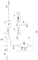
本実施の形態に係る周波数変調器は、VCO、分周器、位相比較器、ループフィルタを用いてPLLを構成し、VCOの入力信号に変調信号を重畳する直接変調型の周波数変調器である。図1は、本発明の実施の形態に係る周波数変調器100の構成を示す回路図である。周波数変調器100は、入力端子102に入力された変調信号である入力信号Sinにもとづき周波数変調を行い、出力端子104から被変調信号Soutを出力する。基準クロック端子106には、基準クロック信号CKrefが入力される。本実施の形態において、入力信号Sinは、所定の直流バイアスが与えられており、たとえば、電源電位と接地電位の中点(Vcc/2)にバイアスされている。
The frequency modulator according to the present embodiment is a direct modulation type frequency modulator that configures a PLL using a VCO, a frequency divider, a phase comparator, and a loop filter, and superimposes a modulation signal on the input signal of the VCO. . FIG. 1 is a circuit diagram showing a configuration of a
周波数変調器100は、演算増幅器10、VCO12、分周器14、位相比較器16、ループフィルタ18、第1抵抗R1、第2抵抗R2を含み、1つの半導体基板上に一体集積化される。
The
演算増幅器10は、反転入力端子に第1抵抗R1を介して変調信号である入力信号Sinが入力される。この演算増幅器10には、たとえば、入力および出力電圧範囲が広いレールアンプを用いる。演算増幅器10の回路構成は特に限定されるものではなく、入力段に差動増幅回路を備えるものであればよい。
The
第2抵抗R2は、演算増幅器10の出力端子と反転入力端子間の帰還経路に設けられる。VCO12には、演算増幅器10の出力電圧(以下、制御電圧Vcntという)が入力される。VCO12は、制御電圧Vcntに応じた周波数frfを有する被変調信号Soutを生成する。この出力信号Soutは、出力端子104から外部へと出力されるとともに、分周器14へと入力される。
The second resistor R2 is provided in a feedback path between the output terminal and the inverting input terminal of the
分周器14は、VCO12の出力信号Soutを、1/nに分周し、帰還信号Sfbを出力する。位相比較器16には、分周器14から出力される周波数がfrf/nの帰還信号Sfbを、基準クロック端子106に入力される基準クロック信号CKrefと比較し、2つの信号の位相差に応じた電圧(以下、位相差電圧Vpcという)を出力する。位相比較器16は、どの構成のものを用いてもよく、たとえば、帰還信号Sfbと、基準クロック信号CKrefの位相差に応じて、チャージ信号またはディスチャージ信号を出力する位相比較回路と、チャージ信号またはディスチャージ信号に応じて、キャパシタを充放電するチャージポンプ回路によって構成することができる。
The
ループフィルタ18は、位相比較器16の出力信号である位相差電圧Vpc1の高周波成分を除去する。ループフィルタ18から出力される位相差電圧Vpc2は、演算増幅器10の非反転入力端子へと入力される。本実施の形態において、ループフィルタ18は、第1キャパシタC1、第2キャパシタC2、第3抵抗R3を含むパッシブフィルタにて構成される。第1キャパシタC1は、位相比較器16の出力端子と接地間に設けられる。第2キャパシタC2および第3抵抗R3は直列に接続され、第1キャパシタC1と並列の経路に設けられている。もっとも、ループフィルタ18の構成は実施の形態に限定されるものではなく、所望のカットオフ周波数が得られればいかなる構成であってもよく、また場合によっては、アクティブフィルタで構成してもよい。
The
以上のように構成された周波数変調器100の動作について説明する。
入力端子102に入力される入力信号Sinと、ループフィルタ18から出力される位相差電圧Vpc2と、制御電圧Vcntの間には、以下の関係式(1)が成り立つ。
Vcnt=(1+R2/R1)×Vpc2−R2/R1×Sin …式(1)
The operation of the
The following relational expression (1) is established between the input signal Sin input to the
Vcnt = (1 + R2 / R1) × Vpc2−R2 / R1 × Sin Formula (1)
すなわち、演算増幅器10、第1抵抗R1、第2抵抗R2は、入力端子102に入力される変調信号である入力信号Sinに対しては、反転アンプとして機能する。この反転アンプの利得G1は、第1抵抗R1、第2抵抗R2の抵抗値で決定され、G1=R2/R1で与えられる。本実施の形態において、R1:R2=10:1程度に設定するものとする。このときの利得G1は、−20dB程度となる。
That is, the
また、演算増幅器10、第1抵抗R1、第2抵抗R2は、ループフィルタ18から出力される位相差電圧Vpc2に対しては、非反転アンプとして機能する。この非反転アンプの利得G2は、第1抵抗R1、第2抵抗R2の抵抗値を用いて、(1+R2/R1)で与えられる。
The
演算増幅器10、第1抵抗R1、第2抵抗R2によって、入力信号Sinとループフィルタ18の出力信号である位相差電圧Vpc2が重畳され、制御電圧Vcntが生成される。VCO12は、制御電圧Vcntに応じた周波数で発振することから、周波数変調器100は、入力信号Sinに応じて周波数変調された被変調信号Soutを生成することができる。
The
この態様によれば、演算増幅器10の入力インピーダンスが高いため、ループフィルタ18のインピーダンスが、入力端子102側の回路に及ぼす影響を低減することができる。その結果、入力信号Sinからは、ループフィルタ18が見えないため、ループフィルタ18により、入力信号Sinの高域が減衰するのを防止し、信号の歪みを抑えることができる。
According to this aspect, since the input impedance of the
また、従来のように抵抗およびキャパシタを用いてカップリングする場合、ループフィルタ18から出力される信号が、入力信号Sin側にリークする場合があったが、本実施の形態に係る周波数変調器100においては、演算増幅器10の入力インピーダンスが高いため、この問題も解消することができる。
Further, when coupling is performed using a resistor and a capacitor as in the prior art, the signal output from the
さらに、従来技術において、カップリングキャパシタを用いる場合、このキャパシタが他の回路素子とともにハイパスフィルタを構成するため、その容量値を非常に大きくする必要があり、IC化できず、外付け部品として設ける必要があった。これに対して、本実施の形態に係る周波数変調器100では、カップリングキャパシタを用いなくても、入力信号SinをPLLのVCO12の入力に重畳することができるため、外付け部品を減らすことができる。また、カップリングキャパシタを外部に設ける場合、2つの端子を設ける必要があったが、これらの端子も削減し、チップ面積を低減することができる。
Furthermore, when a coupling capacitor is used in the prior art, since this capacitor constitutes a high-pass filter together with other circuit elements, the capacitance value needs to be very large and cannot be made into an IC, and is provided as an external component. There was a need. On the other hand, in the
第1抵抗R1、第2抵抗R2の少なくとも一方を、可変抵抗として構成してもよい。この場合、VCO12の特性などに応じて、ループゲインや入力信号の振幅を調節することができる。
At least one of the first resistor R1 and the second resistor R2 may be configured as a variable resistor. In this case, the loop gain and the amplitude of the input signal can be adjusted according to the characteristics of the
演算増幅器10にレールアンプを用いた場合、VCO12の入力信号である制御電圧Vcntの電圧範囲を広く設定することができるため、周波数変調器100から出力される高周波信号の周波数帯を広くとることができる。
When a rail amplifier is used as the
次に、本実施の形態に係る周波数変調器100の応用例について説明する。図2は、図1の周波数変調器100を使用したFM送信機200の構成を示すブロック図である。このFM送信機200は、オーディオ信号をステレオコンポジット信号に変換し、周波数変調を行い、増幅してアンテナから送信する。このようなFM送信機200は、車載用オーディオにおいて、ケーブルを介さずに信号を送信する際に使用したり、あるいは携帯端末に内蔵され、据え置き型のオーディオ機器に対してオーディオ信号を送信する用途に用いることができる。FM送信機200は、図1の周波数変調器100に加えて、ステレオ変調部202、パワーアンプ204を含んで、ひとつのLSIに集積化されてもよいし、別々のICに分割して構成されてもよい。
Next, an application example of the
オーディオ信号源210は、CDプレイヤやMDプレイヤ、メモリオーディオ、ハードディスクオーディオなどであって、オーディオ信号S1を生成し、FM送信機200へと出力する。ステレオ変調部202は、オーディオ信号S1をステレオコンポジット信号S2に変換する。ステレオコンポジット信号S2は、図1の周波数変調器100へと入力される。周波数変調器100は、ステレオコンポジット信号S2にもとづき周波数変調を行い、被変調信号S3(Sout)を生成する。周波数変調器100から出力される被変調信号S3は、パワーアンプ204によって増幅され、アンテナ220から送信される。なお、図2のFM送信機200は主要なブロックのみを簡略化して示すものであり、その他にフィルタなどの回路ブロックは省略している。
The
図2のFM送信機200は、図1の周波数変調器100を用いて構成するため、部品点数が低減されるために小型化が容易となる。その結果、携帯電話端末などへの実装が容易となる。
Since the
実施の形態は例示であり、それらの各構成要素や各処理プロセスの組合せにいろいろな変形例が可能なこと、またそうした変形例も本発明の範囲にあることは当業者に理解されるところである。 The embodiments are exemplifications, and it will be understood by those skilled in the art that various modifications can be made to combinations of the respective constituent elements and processing processes, and such modifications are within the scope of the present invention. .
実施の形態では、演算増幅器10、第1抵抗R1、第2抵抗R2を用いた構成としたが、これにキャパシタなどを付加してフィルタ機能を設けてもよい。また、ループフィルタ18としてアクティブフィルタを用いてもよい。
In the embodiment, the
100 周波数変調器、 10 演算増幅器、 12 VCO、 14 分周器、 16 位相比較器、 18 ループフィルタ、 R1 第1抵抗、 R2 第2抵抗、 102 入力端子、 104 出力端子、 106 基準クロック端子、 C1 第1キャパシタ、 C2 第2キャパシタ、 R3 第3抵抗、 200 FM送信機。 100 frequency modulator, 10 operational amplifier, 12 VCO, 14 frequency divider, 16 phase comparator, 18 loop filter, R1 first resistor, R2 second resistor, 102 input terminal, 104 output terminal, 106 reference clock terminal, C1 1st capacitor, C2 2nd capacitor, R3 3rd resistance, 200 FM transmitter.
Claims (8)
前記演算増幅器の出力端子と反転入力端子間の帰還経路に設けられた第2抵抗と、
前記演算増幅器の出力信号が入力された電圧制御発振器と、
前記電圧制御発振器の出力信号を分周する分周器と、
前記分周器の出力信号を、基準クロック信号と比較し、位相差に応じた電圧を出力する位相比較器と、
前記位相比較器の出力電圧の高周波成分を除去し、前記演算増幅器の非反転入力端子へと出力するフィルタと、
を備えることを特徴とする周波数変調器。 An operational amplifier in which an input signal is input to the inverting input terminal via the first resistor;
A second resistor provided in a feedback path between the output terminal and the inverting input terminal of the operational amplifier;
A voltage controlled oscillator to which an output signal of the operational amplifier is input;
A frequency divider for dividing the output signal of the voltage controlled oscillator;
A phase comparator that compares the output signal of the frequency divider with a reference clock signal and outputs a voltage corresponding to the phase difference;
A filter that removes a high-frequency component of the output voltage of the phase comparator and outputs the non-inverting input terminal of the operational amplifier;
A frequency modulator comprising:
前記ステレオ変調部から出力されるステレオコンポジット信号にもとづいて周波数変調を行い、被変調信号を出力する請求項1から7のいずれかに記載の周波数変調器と、
前記周波数変調器から出力される被変調信号を増幅する増幅器と、
を備えることを特徴とするFM送信回路。 A stereo modulator that converts the audio signal into a stereo composite signal;
The frequency modulator according to any one of claims 1 to 7, which performs frequency modulation based on a stereo composite signal output from the stereo modulation unit and outputs a modulated signal;
An amplifier for amplifying the modulated signal output from the frequency modulator;
An FM transmitter circuit comprising:
Priority Applications (7)
| Application Number | Priority Date | Filing Date | Title |
|---|---|---|---|
| JP2005360968A JP2007166326A (en) | 2005-12-14 | 2005-12-14 | Frequency modulator unit, and fm transmitter circuit using the same |
| US12/096,528 US7936228B2 (en) | 2005-12-06 | 2006-12-05 | Frequency modulator and FM transmission circuit using the same |
| CN2010101098992A CN101877588B (en) | 2005-12-06 | 2006-12-05 | Frequency modulator and fm transmission circuit using the same |
| KR1020077025745A KR20080071484A (en) | 2005-12-06 | 2006-12-05 | Frequency Modulator and FMM Transmission Circuit Using the Same |
| PCT/JP2006/324292 WO2007066672A1 (en) | 2005-12-06 | 2006-12-05 | Frequency modulator and fm transmission circuit using the same |
| TW095145440A TW200733569A (en) | 2005-12-06 | 2006-12-06 | Frequency modulator and fm transmission circuit using the same |
| US13/072,959 US20110170698A1 (en) | 2005-12-06 | 2011-03-28 | Frequency modulator and fm transmission circuit using the same |
Applications Claiming Priority (1)
| Application Number | Priority Date | Filing Date | Title |
|---|---|---|---|
| JP2005360968A JP2007166326A (en) | 2005-12-14 | 2005-12-14 | Frequency modulator unit, and fm transmitter circuit using the same |
Publications (1)
| Publication Number | Publication Date |
|---|---|
| JP2007166326A true JP2007166326A (en) | 2007-06-28 |
Family
ID=38248698
Family Applications (1)
| Application Number | Title | Priority Date | Filing Date |
|---|---|---|---|
| JP2005360968A Pending JP2007166326A (en) | 2005-12-06 | 2005-12-14 | Frequency modulator unit, and fm transmitter circuit using the same |
Country Status (1)
| Country | Link |
|---|---|
| JP (1) | JP2007166326A (en) |
-
2005
- 2005-12-14 JP JP2005360968A patent/JP2007166326A/en active Pending
Similar Documents
| Publication | Publication Date | Title |
|---|---|---|
| US20110170698A1 (en) | Frequency modulator and fm transmission circuit using the same | |
| US9525390B2 (en) | Switching circuit | |
| US9172354B2 (en) | Analog active low-pass filters | |
| US8228132B2 (en) | Voltage-controlled oscillator robust against power noise and communication apparatus using the same | |
| JP2005072031A (en) | High-frequency semiconductor device, communication electronic component, and wireless communication system | |
| US9614702B2 (en) | Technique for crosstalk reduction | |
| US7227392B2 (en) | Frequency multiplier | |
| US8054137B2 (en) | Method and apparatus for integrating a FLL loop filter in polar transmitters | |
| KR20020073264A (en) | Filter circuit, semiconductor device, filter system and signal frequency control method | |
| US7750730B2 (en) | Bandpass filter circuit | |
| US20070237333A1 (en) | FM transmitter using switched capacitor filter | |
| US6480046B1 (en) | Transmitter apparatus and methods using frequency doubling modulation | |
| JP2007166326A (en) | Frequency modulator unit, and fm transmitter circuit using the same | |
| JP2007158857A (en) | Fm transmission circuit | |
| US20070195961A1 (en) | FM transmitter | |
| JP2005260787A (en) | Phase shifter | |
| JP2007159006A (en) | Fm transmission circuit | |
| US7667553B2 (en) | Frequency modulator using PLL | |
| US10594342B1 (en) | Power amplifying system and associated power amplifying method for bluetooth device | |
| JP3429657B2 (en) | Divider | |
| JP4113838B2 (en) | Receiver and composite parts | |
| JP2007116247A (en) | Orthogonal signal generation circuit, and reception tuner and communication device including the same | |
| JP2007067647A (en) | Voltage controlled oscillator circuit | |
| JP3399572B2 (en) | IQ demodulator | |
| JP3957312B2 (en) | FM transmitter |
Legal Events
| Date | Code | Title | Description |
|---|---|---|---|
| A521 | Written amendment |
Free format text: JAPANESE INTERMEDIATE CODE: A523 Effective date: 20070426 |
|
| A02 | Decision of refusal |
Free format text: JAPANESE INTERMEDIATE CODE: A02 Effective date: 20080401 |