JP2007142436A - Semiconductor device comprising lineup mark film and method of manufacturing same - Google Patents
Semiconductor device comprising lineup mark film and method of manufacturing same Download PDFInfo
- Publication number
- JP2007142436A JP2007142436A JP2006313358A JP2006313358A JP2007142436A JP 2007142436 A JP2007142436 A JP 2007142436A JP 2006313358 A JP2006313358 A JP 2006313358A JP 2006313358 A JP2006313358 A JP 2006313358A JP 2007142436 A JP2007142436 A JP 2007142436A
- Authority
- JP
- Japan
- Prior art keywords
- film
- pad electrode
- alignment mark
- passivation
- semiconductor device
- Prior art date
- Legal status (The legal status is an assumption and is not a legal conclusion. Google has not performed a legal analysis and makes no representation as to the accuracy of the status listed.)
- Pending
Links
Images


Classifications
-
- H—ELECTRICITY
- H01—ELECTRIC ELEMENTS
- H01L—SEMICONDUCTOR DEVICES NOT COVERED BY CLASS H10
- H01L23/00—Details of semiconductor or other solid state devices
- H01L23/544—Marks applied to semiconductor devices or parts, e.g. registration marks, alignment structures, wafer maps
-
- H—ELECTRICITY
- H01—ELECTRIC ELEMENTS
- H01L—SEMICONDUCTOR DEVICES NOT COVERED BY CLASS H10
- H01L23/00—Details of semiconductor or other solid state devices
- H01L23/12—Mountings, e.g. non-detachable insulating substrates
-
- H—ELECTRICITY
- H01—ELECTRIC ELEMENTS
- H01L—SEMICONDUCTOR DEVICES NOT COVERED BY CLASS H10
- H01L24/00—Arrangements for connecting or disconnecting semiconductor or solid-state bodies; Methods or apparatus related thereto
- H01L24/01—Means for bonding being attached to, or being formed on, the surface to be connected, e.g. chip-to-package, die-attach, "first-level" interconnects; Manufacturing methods related thereto
- H01L24/02—Bonding areas ; Manufacturing methods related thereto
- H01L24/03—Manufacturing methods
-
- H—ELECTRICITY
- H01—ELECTRIC ELEMENTS
- H01L—SEMICONDUCTOR DEVICES NOT COVERED BY CLASS H10
- H01L24/00—Arrangements for connecting or disconnecting semiconductor or solid-state bodies; Methods or apparatus related thereto
- H01L24/01—Means for bonding being attached to, or being formed on, the surface to be connected, e.g. chip-to-package, die-attach, "first-level" interconnects; Manufacturing methods related thereto
- H01L24/10—Bump connectors ; Manufacturing methods related thereto
- H01L24/11—Manufacturing methods
-
- H—ELECTRICITY
- H01—ELECTRIC ELEMENTS
- H01L—SEMICONDUCTOR DEVICES NOT COVERED BY CLASS H10
- H01L2223/00—Details relating to semiconductor or other solid state devices covered by the group H01L23/00
- H01L2223/544—Marks applied to semiconductor devices or parts
- H01L2223/54426—Marks applied to semiconductor devices or parts for alignment
-
- H—ELECTRICITY
- H01—ELECTRIC ELEMENTS
- H01L—SEMICONDUCTOR DEVICES NOT COVERED BY CLASS H10
- H01L2223/00—Details relating to semiconductor or other solid state devices covered by the group H01L23/00
- H01L2223/544—Marks applied to semiconductor devices or parts
- H01L2223/54473—Marks applied to semiconductor devices or parts for use after dicing
- H01L2223/5448—Located on chip prior to dicing and remaining on chip after dicing
-
- H—ELECTRICITY
- H01—ELECTRIC ELEMENTS
- H01L—SEMICONDUCTOR DEVICES NOT COVERED BY CLASS H10
- H01L2224/00—Indexing scheme for arrangements for connecting or disconnecting semiconductor or solid-state bodies and methods related thereto as covered by H01L24/00
- H01L2224/01—Means for bonding being attached to, or being formed on, the surface to be connected, e.g. chip-to-package, die-attach, "first-level" interconnects; Manufacturing methods related thereto
- H01L2224/02—Bonding areas; Manufacturing methods related thereto
- H01L2224/03—Manufacturing methods
- H01L2224/039—Methods of manufacturing bonding areas involving a specific sequence of method steps
- H01L2224/03912—Methods of manufacturing bonding areas involving a specific sequence of method steps the bump being used as a mask for patterning the bonding area
-
- H—ELECTRICITY
- H01—ELECTRIC ELEMENTS
- H01L—SEMICONDUCTOR DEVICES NOT COVERED BY CLASS H10
- H01L2224/00—Indexing scheme for arrangements for connecting or disconnecting semiconductor or solid-state bodies and methods related thereto as covered by H01L24/00
- H01L2224/01—Means for bonding being attached to, or being formed on, the surface to be connected, e.g. chip-to-package, die-attach, "first-level" interconnects; Manufacturing methods related thereto
- H01L2224/02—Bonding areas; Manufacturing methods related thereto
- H01L2224/04—Structure, shape, material or disposition of the bonding areas prior to the connecting process
- H01L2224/0401—Bonding areas specifically adapted for bump connectors, e.g. under bump metallisation [UBM]
-
- H—ELECTRICITY
- H01—ELECTRIC ELEMENTS
- H01L—SEMICONDUCTOR DEVICES NOT COVERED BY CLASS H10
- H01L2224/00—Indexing scheme for arrangements for connecting or disconnecting semiconductor or solid-state bodies and methods related thereto as covered by H01L24/00
- H01L2224/01—Means for bonding being attached to, or being formed on, the surface to be connected, e.g. chip-to-package, die-attach, "first-level" interconnects; Manufacturing methods related thereto
- H01L2224/02—Bonding areas; Manufacturing methods related thereto
- H01L2224/04—Structure, shape, material or disposition of the bonding areas prior to the connecting process
- H01L2224/05—Structure, shape, material or disposition of the bonding areas prior to the connecting process of an individual bonding area
- H01L2224/0554—External layer
- H01L2224/0555—Shape
- H01L2224/05556—Shape in side view
-
- H—ELECTRICITY
- H01—ELECTRIC ELEMENTS
- H01L—SEMICONDUCTOR DEVICES NOT COVERED BY CLASS H10
- H01L2224/00—Indexing scheme for arrangements for connecting or disconnecting semiconductor or solid-state bodies and methods related thereto as covered by H01L24/00
- H01L2224/01—Means for bonding being attached to, or being formed on, the surface to be connected, e.g. chip-to-package, die-attach, "first-level" interconnects; Manufacturing methods related thereto
- H01L2224/02—Bonding areas; Manufacturing methods related thereto
- H01L2224/04—Structure, shape, material or disposition of the bonding areas prior to the connecting process
- H01L2224/05—Structure, shape, material or disposition of the bonding areas prior to the connecting process of an individual bonding area
- H01L2224/0554—External layer
- H01L2224/0556—Disposition
- H01L2224/05571—Disposition the external layer being disposed in a recess of the surface
- H01L2224/05572—Disposition the external layer being disposed in a recess of the surface the external layer extending out of an opening
-
- H—ELECTRICITY
- H01—ELECTRIC ELEMENTS
- H01L—SEMICONDUCTOR DEVICES NOT COVERED BY CLASS H10
- H01L2224/00—Indexing scheme for arrangements for connecting or disconnecting semiconductor or solid-state bodies and methods related thereto as covered by H01L24/00
- H01L2224/01—Means for bonding being attached to, or being formed on, the surface to be connected, e.g. chip-to-package, die-attach, "first-level" interconnects; Manufacturing methods related thereto
- H01L2224/10—Bump connectors; Manufacturing methods related thereto
- H01L2224/11—Manufacturing methods
- H01L2224/1147—Manufacturing methods using a lift-off mask
- H01L2224/11474—Multilayer masks
-
- H—ELECTRICITY
- H01—ELECTRIC ELEMENTS
- H01L—SEMICONDUCTOR DEVICES NOT COVERED BY CLASS H10
- H01L2224/00—Indexing scheme for arrangements for connecting or disconnecting semiconductor or solid-state bodies and methods related thereto as covered by H01L24/00
- H01L2224/01—Means for bonding being attached to, or being formed on, the surface to be connected, e.g. chip-to-package, die-attach, "first-level" interconnects; Manufacturing methods related thereto
- H01L2224/10—Bump connectors; Manufacturing methods related thereto
- H01L2224/12—Structure, shape, material or disposition of the bump connectors prior to the connecting process
- H01L2224/13—Structure, shape, material or disposition of the bump connectors prior to the connecting process of an individual bump connector
- H01L2224/13001—Core members of the bump connector
- H01L2224/1302—Disposition
- H01L2224/13021—Disposition the bump connector being disposed in a recess of the surface
-
- H—ELECTRICITY
- H01—ELECTRIC ELEMENTS
- H01L—SEMICONDUCTOR DEVICES NOT COVERED BY CLASS H10
- H01L2224/00—Indexing scheme for arrangements for connecting or disconnecting semiconductor or solid-state bodies and methods related thereto as covered by H01L24/00
- H01L2224/01—Means for bonding being attached to, or being formed on, the surface to be connected, e.g. chip-to-package, die-attach, "first-level" interconnects; Manufacturing methods related thereto
- H01L2224/10—Bump connectors; Manufacturing methods related thereto
- H01L2224/12—Structure, shape, material or disposition of the bump connectors prior to the connecting process
- H01L2224/13—Structure, shape, material or disposition of the bump connectors prior to the connecting process of an individual bump connector
- H01L2224/13001—Core members of the bump connector
- H01L2224/13099—Material
- H01L2224/131—Material with a principal constituent of the material being a metal or a metalloid, e.g. boron [B], silicon [Si], germanium [Ge], arsenic [As], antimony [Sb], tellurium [Te] and polonium [Po], and alloys thereof
- H01L2224/13138—Material with a principal constituent of the material being a metal or a metalloid, e.g. boron [B], silicon [Si], germanium [Ge], arsenic [As], antimony [Sb], tellurium [Te] and polonium [Po], and alloys thereof the principal constituent melting at a temperature of greater than or equal to 950°C and less than 1550°C
- H01L2224/13144—Gold [Au] as principal constituent
-
- H—ELECTRICITY
- H01—ELECTRIC ELEMENTS
- H01L—SEMICONDUCTOR DEVICES NOT COVERED BY CLASS H10
- H01L2224/00—Indexing scheme for arrangements for connecting or disconnecting semiconductor or solid-state bodies and methods related thereto as covered by H01L24/00
- H01L2224/01—Means for bonding being attached to, or being formed on, the surface to be connected, e.g. chip-to-package, die-attach, "first-level" interconnects; Manufacturing methods related thereto
- H01L2224/10—Bump connectors; Manufacturing methods related thereto
- H01L2224/15—Structure, shape, material or disposition of the bump connectors after the connecting process
- H01L2224/16—Structure, shape, material or disposition of the bump connectors after the connecting process of an individual bump connector
-
- H—ELECTRICITY
- H01—ELECTRIC ELEMENTS
- H01L—SEMICONDUCTOR DEVICES NOT COVERED BY CLASS H10
- H01L2224/00—Indexing scheme for arrangements for connecting or disconnecting semiconductor or solid-state bodies and methods related thereto as covered by H01L24/00
- H01L2224/80—Methods for connecting semiconductor or other solid state bodies using means for bonding being attached to, or being formed on, the surface to be connected
- H01L2224/81—Methods for connecting semiconductor or other solid state bodies using means for bonding being attached to, or being formed on, the surface to be connected using a bump connector
- H01L2224/8112—Aligning
- H01L2224/81121—Active alignment, i.e. by apparatus steering, e.g. optical alignment using marks or sensors
-
- H—ELECTRICITY
- H01—ELECTRIC ELEMENTS
- H01L—SEMICONDUCTOR DEVICES NOT COVERED BY CLASS H10
- H01L2224/00—Indexing scheme for arrangements for connecting or disconnecting semiconductor or solid-state bodies and methods related thereto as covered by H01L24/00
- H01L2224/80—Methods for connecting semiconductor or other solid state bodies using means for bonding being attached to, or being formed on, the surface to be connected
- H01L2224/81—Methods for connecting semiconductor or other solid state bodies using means for bonding being attached to, or being formed on, the surface to be connected using a bump connector
- H01L2224/818—Bonding techniques
- H01L2224/81801—Soldering or alloying
-
- H—ELECTRICITY
- H01—ELECTRIC ELEMENTS
- H01L—SEMICONDUCTOR DEVICES NOT COVERED BY CLASS H10
- H01L24/00—Arrangements for connecting or disconnecting semiconductor or solid-state bodies; Methods or apparatus related thereto
- H01L24/01—Means for bonding being attached to, or being formed on, the surface to be connected, e.g. chip-to-package, die-attach, "first-level" interconnects; Manufacturing methods related thereto
- H01L24/10—Bump connectors ; Manufacturing methods related thereto
- H01L24/12—Structure, shape, material or disposition of the bump connectors prior to the connecting process
-
- H—ELECTRICITY
- H01—ELECTRIC ELEMENTS
- H01L—SEMICONDUCTOR DEVICES NOT COVERED BY CLASS H10
- H01L24/00—Arrangements for connecting or disconnecting semiconductor or solid-state bodies; Methods or apparatus related thereto
- H01L24/80—Methods for connecting semiconductor or other solid state bodies using means for bonding being attached to, or being formed on, the surface to be connected
- H01L24/81—Methods for connecting semiconductor or other solid state bodies using means for bonding being attached to, or being formed on, the surface to be connected using a bump connector
-
- H—ELECTRICITY
- H01—ELECTRIC ELEMENTS
- H01L—SEMICONDUCTOR DEVICES NOT COVERED BY CLASS H10
- H01L2924/00—Indexing scheme for arrangements or methods for connecting or disconnecting semiconductor or solid-state bodies as covered by H01L24/00
- H01L2924/01—Chemical elements
- H01L2924/01004—Beryllium [Be]
-
- H—ELECTRICITY
- H01—ELECTRIC ELEMENTS
- H01L—SEMICONDUCTOR DEVICES NOT COVERED BY CLASS H10
- H01L2924/00—Indexing scheme for arrangements or methods for connecting or disconnecting semiconductor or solid-state bodies as covered by H01L24/00
- H01L2924/01—Chemical elements
- H01L2924/01005—Boron [B]
-
- H—ELECTRICITY
- H01—ELECTRIC ELEMENTS
- H01L—SEMICONDUCTOR DEVICES NOT COVERED BY CLASS H10
- H01L2924/00—Indexing scheme for arrangements or methods for connecting or disconnecting semiconductor or solid-state bodies as covered by H01L24/00
- H01L2924/01—Chemical elements
- H01L2924/01006—Carbon [C]
-
- H—ELECTRICITY
- H01—ELECTRIC ELEMENTS
- H01L—SEMICONDUCTOR DEVICES NOT COVERED BY CLASS H10
- H01L2924/00—Indexing scheme for arrangements or methods for connecting or disconnecting semiconductor or solid-state bodies as covered by H01L24/00
- H01L2924/01—Chemical elements
- H01L2924/01013—Aluminum [Al]
-
- H—ELECTRICITY
- H01—ELECTRIC ELEMENTS
- H01L—SEMICONDUCTOR DEVICES NOT COVERED BY CLASS H10
- H01L2924/00—Indexing scheme for arrangements or methods for connecting or disconnecting semiconductor or solid-state bodies as covered by H01L24/00
- H01L2924/01—Chemical elements
- H01L2924/01014—Silicon [Si]
-
- H—ELECTRICITY
- H01—ELECTRIC ELEMENTS
- H01L—SEMICONDUCTOR DEVICES NOT COVERED BY CLASS H10
- H01L2924/00—Indexing scheme for arrangements or methods for connecting or disconnecting semiconductor or solid-state bodies as covered by H01L24/00
- H01L2924/01—Chemical elements
- H01L2924/01022—Titanium [Ti]
-
- H—ELECTRICITY
- H01—ELECTRIC ELEMENTS
- H01L—SEMICONDUCTOR DEVICES NOT COVERED BY CLASS H10
- H01L2924/00—Indexing scheme for arrangements or methods for connecting or disconnecting semiconductor or solid-state bodies as covered by H01L24/00
- H01L2924/01—Chemical elements
- H01L2924/01028—Nickel [Ni]
-
- H—ELECTRICITY
- H01—ELECTRIC ELEMENTS
- H01L—SEMICONDUCTOR DEVICES NOT COVERED BY CLASS H10
- H01L2924/00—Indexing scheme for arrangements or methods for connecting or disconnecting semiconductor or solid-state bodies as covered by H01L24/00
- H01L2924/01—Chemical elements
- H01L2924/01029—Copper [Cu]
-
- H—ELECTRICITY
- H01—ELECTRIC ELEMENTS
- H01L—SEMICONDUCTOR DEVICES NOT COVERED BY CLASS H10
- H01L2924/00—Indexing scheme for arrangements or methods for connecting or disconnecting semiconductor or solid-state bodies as covered by H01L24/00
- H01L2924/01—Chemical elements
- H01L2924/01033—Arsenic [As]
-
- H—ELECTRICITY
- H01—ELECTRIC ELEMENTS
- H01L—SEMICONDUCTOR DEVICES NOT COVERED BY CLASS H10
- H01L2924/00—Indexing scheme for arrangements or methods for connecting or disconnecting semiconductor or solid-state bodies as covered by H01L24/00
- H01L2924/01—Chemical elements
- H01L2924/01073—Tantalum [Ta]
-
- H—ELECTRICITY
- H01—ELECTRIC ELEMENTS
- H01L—SEMICONDUCTOR DEVICES NOT COVERED BY CLASS H10
- H01L2924/00—Indexing scheme for arrangements or methods for connecting or disconnecting semiconductor or solid-state bodies as covered by H01L24/00
- H01L2924/01—Chemical elements
- H01L2924/01078—Platinum [Pt]
-
- H—ELECTRICITY
- H01—ELECTRIC ELEMENTS
- H01L—SEMICONDUCTOR DEVICES NOT COVERED BY CLASS H10
- H01L2924/00—Indexing scheme for arrangements or methods for connecting or disconnecting semiconductor or solid-state bodies as covered by H01L24/00
- H01L2924/01—Chemical elements
- H01L2924/01079—Gold [Au]
-
- H—ELECTRICITY
- H01—ELECTRIC ELEMENTS
- H01L—SEMICONDUCTOR DEVICES NOT COVERED BY CLASS H10
- H01L2924/00—Indexing scheme for arrangements or methods for connecting or disconnecting semiconductor or solid-state bodies as covered by H01L24/00
- H01L2924/01—Chemical elements
- H01L2924/01082—Lead [Pb]
-
- H—ELECTRICITY
- H01—ELECTRIC ELEMENTS
- H01L—SEMICONDUCTOR DEVICES NOT COVERED BY CLASS H10
- H01L2924/00—Indexing scheme for arrangements or methods for connecting or disconnecting semiconductor or solid-state bodies as covered by H01L24/00
- H01L2924/013—Alloys
- H01L2924/014—Solder alloys
-
- H—ELECTRICITY
- H01—ELECTRIC ELEMENTS
- H01L—SEMICONDUCTOR DEVICES NOT COVERED BY CLASS H10
- H01L2924/00—Indexing scheme for arrangements or methods for connecting or disconnecting semiconductor or solid-state bodies as covered by H01L24/00
- H01L2924/049—Nitrides composed of metals from groups of the periodic table
- H01L2924/0494—4th Group
- H01L2924/04941—TiN
-
- H—ELECTRICITY
- H01—ELECTRIC ELEMENTS
- H01L—SEMICONDUCTOR DEVICES NOT COVERED BY CLASS H10
- H01L2924/00—Indexing scheme for arrangements or methods for connecting or disconnecting semiconductor or solid-state bodies as covered by H01L24/00
- H01L2924/049—Nitrides composed of metals from groups of the periodic table
- H01L2924/0495—5th Group
- H01L2924/04953—TaN
-
- H—ELECTRICITY
- H01—ELECTRIC ELEMENTS
- H01L—SEMICONDUCTOR DEVICES NOT COVERED BY CLASS H10
- H01L2924/00—Indexing scheme for arrangements or methods for connecting or disconnecting semiconductor or solid-state bodies as covered by H01L24/00
- H01L2924/049—Nitrides composed of metals from groups of the periodic table
- H01L2924/0504—14th Group
- H01L2924/05042—Si3N4
-
- H—ELECTRICITY
- H01—ELECTRIC ELEMENTS
- H01L—SEMICONDUCTOR DEVICES NOT COVERED BY CLASS H10
- H01L2924/00—Indexing scheme for arrangements or methods for connecting or disconnecting semiconductor or solid-state bodies as covered by H01L24/00
- H01L2924/19—Details of hybrid assemblies other than the semiconductor or other solid state devices to be connected
- H01L2924/1901—Structure
- H01L2924/1904—Component type
- H01L2924/19041—Component type being a capacitor
-
- H—ELECTRICITY
- H01—ELECTRIC ELEMENTS
- H01L—SEMICONDUCTOR DEVICES NOT COVERED BY CLASS H10
- H01L2924/00—Indexing scheme for arrangements or methods for connecting or disconnecting semiconductor or solid-state bodies as covered by H01L24/00
- H01L2924/19—Details of hybrid assemblies other than the semiconductor or other solid state devices to be connected
- H01L2924/1901—Structure
- H01L2924/1904—Component type
- H01L2924/19043—Component type being a resistor
-
- Y—GENERAL TAGGING OF NEW TECHNOLOGICAL DEVELOPMENTS; GENERAL TAGGING OF CROSS-SECTIONAL TECHNOLOGIES SPANNING OVER SEVERAL SECTIONS OF THE IPC; TECHNICAL SUBJECTS COVERED BY FORMER USPC CROSS-REFERENCE ART COLLECTIONS [XRACs] AND DIGESTS
- Y10—TECHNICAL SUBJECTS COVERED BY FORMER USPC
- Y10S—TECHNICAL SUBJECTS COVERED BY FORMER USPC CROSS-REFERENCE ART COLLECTIONS [XRACs] AND DIGESTS
- Y10S438/00—Semiconductor device manufacturing: process
- Y10S438/975—Substrate or mask aligning feature
Abstract
Description
本発明は、半導体素子及びその製造方法に係り、特に、半導体チップの実装工程の整列キーとして利用される整列マークを有する半導体素子及びその製造方法に関する。 The present invention relates to a semiconductor device and a manufacturing method thereof, and more particularly to a semiconductor device having an alignment mark used as an alignment key in a semiconductor chip mounting process and a manufacturing method thereof.
半導体素子は、半導体基板上に形成された後、外部装置と連結され、外部環境から保護されるために適切な形態に組立てられ、かつパッケージングされる。特に、半導体素子は、外部装置との連結のための入出力端子として利用されるパッド電極膜及び組立工程で整列キーとして利用される整列マークを有する。例えば、液晶ディスプレイ素子(LCD:Liquid Crystal Display)の駆動素子として利用される半導体素子は、ガラス基板上に組立てられる。このような組立方式は、COG(Chip On Glass)方式と呼ばれる。 After the semiconductor device is formed on the semiconductor substrate, the semiconductor device is connected to an external device, assembled in an appropriate form and packaged to be protected from the external environment. In particular, the semiconductor element has a pad electrode film used as an input / output terminal for connection to an external device and an alignment mark used as an alignment key in an assembly process. For example, a semiconductor element used as a driving element of a liquid crystal display element (LCD: Liquid Crystal Display) is assembled on a glass substrate. Such an assembly method is called a COG (Chip On Glass) method.
COG組立方式において、半導体素子は、整列マークを利用してガラス基板に整列されうる。例えば、COG組立方式については、特許文献1の“COG用パネル構造”を参照できる。しかし、従来において、半導体素子の整列マーク構造は、製造工程での工程変化によって、以後整列のエラーを発生させうる。 In the COG assembly method, the semiconductor devices may be aligned on the glass substrate using alignment marks. For example, regarding the COG assembly method, the “COG panel structure” of Patent Document 1 can be referred to. However, conventionally, the alignment mark structure of a semiconductor device may cause an alignment error due to a process change in a manufacturing process.
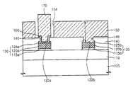
図1は、従来の整列マークの構造を有する半導体素子を示す断面図である。 FIG. 1 is a cross-sectional view illustrating a semiconductor device having a conventional alignment mark structure.
図1を参照すれば、整列マーク膜55は、半導体基板50上に形成され、パッシベーション膜60で取り囲まれている。パッシベーション膜60上には、半導体素子の保護のためにポリイミド膜70が形成される。ポリイミド膜70は、整列マーク膜55上のパッシベーション膜60を露出するようにパターニングされている。通常、整列マーク膜55は、素子分離用絶縁膜で形成されたフィールド領域(図示せず)で取り囲まれている。
Referring to FIG. 1, the
したがって、光学整列装置は、フィールド領域と整列マーク膜55との色相差を認識でき、このような色相差を利用して半導体素子を整列させうる。しかし、半導体素子による整列マーク膜55上のパッシベーション膜60の厚さ(h)の偏差は、整列マーク膜55の色相を変え、このような整列マーク膜55の色相差は、半導体素子の整列のエラーを誘発しうる。それは、光学整列装置は、フィールド領域と整列マーク膜55の基準範囲との色相差を基準として整列を進めるため、その基準範囲を逸脱した半導体素子に対しては、整列作業を進められないためである。
Therefore, the optical alignment apparatus can recognize the hue difference between the field region and the
パッシベーション膜60は、その厚さ(h)の偏差によって色相差が大きく変わる。したがって、パッシベーション膜60の厚さ(h)の調節を通じて色相差を調節することは非常に難しい。これにより、パッシベーション膜60が通常許容される工程マージン範囲内にある場合にも、半導体素子の整列のエラーが発生する恐れがある。
本発明が解決しようとする技術的課題は、前記問題点を克服するために案出されたものであって、組立工程で整列のエラーを減らせる半導体素子を提供することである。 A technical problem to be solved by the present invention is to provide a semiconductor device that has been devised to overcome the above-described problems and can reduce alignment errors in an assembly process.
本発明が解決しようとする他の技術的課題は、組立工程で整列のエラーを減らせ、経済性のある半導体素子の製造方法を提供することである。 Another technical problem to be solved by the present invention is to provide an economical method of manufacturing a semiconductor device, which can reduce alignment errors in an assembly process.
前記課題を達成するための本発明の一態様による半導体素子は、入出力端子として利用される半導体基板上のパッド電極膜を備える。組立工程の整列キーとして利用される整列マーク膜は、前記半導体基板上に形成される。パッシベーション膜は、前記半導体基板上に形成され、前記パッド電極膜の上部の少なくとも一部分及び前記整列マーク膜の上部の少なくとも一部分をそれぞれ露出する。透光性保護膜は、前記パッシベーション膜の少なくとも一部分を覆い、前記パッシベーション膜から露出された前記パッド電極膜の上部を露出し、前記パッシベーション膜から露出された前記整列マーク膜を覆っている。 In order to achieve the above object, a semiconductor element according to one embodiment of the present invention includes a pad electrode film on a semiconductor substrate used as an input / output terminal. An alignment mark film used as an alignment key in the assembly process is formed on the semiconductor substrate. A passivation film is formed on the semiconductor substrate and exposes at least part of the upper part of the pad electrode film and at least part of the upper part of the alignment mark film. The translucent protective film covers at least a part of the passivation film, exposes an upper portion of the pad electrode film exposed from the passivation film, and covers the alignment mark film exposed from the passivation film.
前記本発明の一側面によれば、前記パッド電極膜及び前記整列マーク膜は、同じ物質で形成されうる。例えば、前記パッド電極膜は、障壁金属膜、前記障壁金属膜上の配線金属膜及び前記配線金属膜上のキャッピング金属膜を含み、前記キャッピング金属膜は、前記配線金属膜の少なくとも一部分を露出できる。前記整列マーク膜は、障壁金属膜、前記障壁金属膜上の配線金属膜及び前記配線金属膜上のキャッピング金属膜をさらに含み、前記キャッピング金属膜は、前記配線金属膜の少なくとも一部分を露出できる。 According to the aspect of the present invention, the pad electrode film and the alignment mark film may be formed of the same material. For example, the pad electrode film includes a barrier metal film, a wiring metal film on the barrier metal film, and a capping metal film on the wiring metal film, and the capping metal film can expose at least a part of the wiring metal film. . The alignment mark film further includes a barrier metal film, a wiring metal film on the barrier metal film, and a capping metal film on the wiring metal film, and the capping metal film may expose at least a part of the wiring metal film.
前記本発明の他の側面によれば、前記半導体素子は、前記パッシベーション膜及び前記透光性保護膜から露出された前記パッド電極膜の配線金属膜上のバンプをさらに含みうる。さらに、前記半導体素子は、前記パッド電極膜の配線金属膜と前記バンプとの間、及び前記バンプと前記パッシベーション膜との間にそれぞれ介在された第2障壁金属膜をさらに含みうる。 According to another aspect of the present invention, the semiconductor device may further include a bump on the wiring metal film of the pad electrode film exposed from the passivation film and the translucent protective film. Further, the semiconductor device may further include a second barrier metal film interposed between the wiring metal film of the pad electrode film and the bump and between the bump and the passivation film.
前記課題を達成するための本発明の他の態様による半導体素子は、半導体基板上の層間絶縁膜を備える。入出力端子として利用されるパッド電極膜は、前記層間絶縁膜上に形成される。組立工程の整列キーとして利用される整列マーク膜は、前記層間絶縁膜上に形成される。パッシベーション膜は、前記層間絶縁膜上に形成され、前記パッド電極膜の上部の少なくとも一部分及び前記整列マーク膜の上部の少なくとも一部分をそれぞれ露出する。ポリイミド膜は、前記パッシベーション膜の少なくとも一部分を覆い、前記パッシベーション膜から露出された前記パッド電極膜の上部を露出し、前記パッシベーション膜から露出された前記整列マーク膜部分を覆っている。バンプは、前記パッシベーション膜及びポリイミド膜から露出された前記パッド電極膜上に提供される。 In order to achieve the above object, a semiconductor device according to another aspect of the present invention includes an interlayer insulating film on a semiconductor substrate. A pad electrode film used as an input / output terminal is formed on the interlayer insulating film. An alignment mark film used as an alignment key in the assembly process is formed on the interlayer insulating film. A passivation film is formed on the interlayer insulating film and exposes at least part of the upper part of the pad electrode film and at least part of the upper part of the alignment mark film. The polyimide film covers at least a part of the passivation film, exposes the upper part of the pad electrode film exposed from the passivation film, and covers the alignment mark film part exposed from the passivation film. The bump is provided on the pad electrode film exposed from the passivation film and the polyimide film.
前記他の課題を達成するための本発明の一態様による半導体素子の製造方法によれば、半導体基板上に入出力端子として利用されるパッド電極膜及び組立工程の整列キーとして利用される整列マーク膜を形成する。前記半導体基板上に前記パッド電極膜の上部の少なくとも一部分及び前記整列マーク膜の上部の少なくとも一部分をそれぞれ露出するパッシベーション膜を形成する。前記パッシベーション膜が形成された結果物上に、前記パッシベーション膜から露出された前記パッド電極膜の上部を露出し、前記パッシベーション膜から露出された前記整列マーク膜を覆っている透光性保護膜を形成する。 According to a method of manufacturing a semiconductor device according to an aspect of the present invention for achieving the other object, a pad electrode film used as an input / output terminal on a semiconductor substrate and an alignment mark used as an alignment key for an assembly process A film is formed. A passivation film exposing at least a part of the upper part of the pad electrode film and at least a part of the upper part of the alignment mark film is formed on the semiconductor substrate. A translucent protective film that exposes an upper portion of the pad electrode film exposed from the passivation film and covers the alignment mark film exposed from the passivation film is formed on the resultant product on which the passivation film is formed. Form.
前記本発明の一側面によれば、前記半導体素子の製造方法は、前記パッシベーション膜及び前記透光性保護膜から露出された前記パッド電極膜上にバンプを形成する工程をさらに含みうる。前記バンプは、メッキを利用して形成されうる。 According to another aspect of the present invention, the method of manufacturing a semiconductor device may further include a step of forming a bump on the pad electrode film exposed from the passivation film and the translucent protective film. The bump may be formed using plating.
本発明による半導体素子によれば、透光性保護膜の形成工程において、工程変化によってその厚さが変化されても、整列マーク膜の色相は一定に維持されうる。すなわち、フィールド領域と整列マーク膜との色相差が一定に維持されうる。これにより、光整列装置は、透光性保護膜の厚さが若干異なっても、半導体素子をエラーなしに整列させうる。例えば、COG方式の組立工程で、半導体素子及びガラス基板は、整列マーク膜を利用してエラーなしに整列されうる。 According to the semiconductor device of the present invention, the hue of the alignment mark film can be maintained constant even when the thickness of the translucent protective film is changed due to process changes. That is, the hue difference between the field region and the alignment mark film can be kept constant. As a result, the optical alignment device can align the semiconductor elements without error even if the thickness of the translucent protective film is slightly different. For example, in the COG assembly process, the semiconductor device and the glass substrate may be aligned without error using an alignment mark film.
本発明による半導体素子の製造方法によれば、第2障壁金属層の一部分の除去工程の間に、透光性保護膜は、整列マーク膜を保護するエッチングマスクの役割を行える。これにより、第2障壁金属層の一部分の除去工程が簡素化され、整列マーク膜の一部分の損傷が防止されうる。 According to the method for manufacturing a semiconductor device of the present invention, the translucent protective film can serve as an etching mask for protecting the alignment mark film during the step of removing a portion of the second barrier metal layer. This simplifies the process of removing a portion of the second barrier metal layer and prevents damage to a portion of the alignment mark film.
以下、添付した図面を参照して本発明による望ましい実施形態を説明することによって、本発明を詳細に説明する。しかし、本発明は、後述する実施形態に限定されず、異なる多様な形態で具現され、単に本実施形態は、本発明の開示を完全にし、当業者に発明の範囲を完全に知らせるために提供されるものである。図面で、構成要素は、説明の便宜のためにそのサイズが誇張されうる。 Hereinafter, exemplary embodiments of the present invention will be described in detail with reference to the accompanying drawings. However, the present invention is not limited to the embodiments described below, but may be embodied in various different forms. The embodiments are merely provided to complete the disclosure of the present invention and to fully inform the skilled person of the scope of the invention. It is what is done. In the drawings, the size of components may be exaggerated for convenience of description.
[構造]
図2は、本発明の実施形態による半導体素子を示す平面図であり、図3は、図2の半導体素子のIII−III’線で切り取った断面図である。本発明の実施形態による半導体素子は、LCDの駆動素子を含みうるが、これに制限されるものではない。例えば、本発明の実施形態による半導体素子は、COG方式の組立用半導体素子を含みうる。
[Construction]
2 is a plan view illustrating a semiconductor device according to an embodiment of the present invention, and FIG. 3 is a cross-sectional view taken along line III-III ′ of the semiconductor device of FIG. The semiconductor device according to the embodiment of the present invention may include an LCD driving device, but is not limited thereto. For example, the semiconductor device according to the embodiment of the present invention may include a COG assembly semiconductor device.
図2を参照すれば、本発明の実施形態による半導体素子は、少なくとも一つ以上の整列マーク膜135,136,137,138及び少なくとも一つ以上のバンプ170を含みうる。整列マーク膜135,136,137,138は、半導体素子の組立工程で整列キーとして利用されうる。整列マーク膜135,136,137,138は、透光性保護膜150で覆われている。バンプ170は、半導体素子と外部装置(図示せず)との連結を助ける役割を行える。例えば、バンプ170は、ソルダーバンプでありうる。整列マーク膜135,136,137,138は、素子分離用絶縁膜で形成されたフィールド領域(図示せず)によって取り囲まれうる。
Referring to FIG. 2, the semiconductor device according to the embodiment of the present invention may include at least one
図2に示された整列マーク膜135,136,137,138の数及びバンプ170の数は、例示的なものであり、当業者によって適切な数が選択されうる。整列マーク膜135,136,137,138は、“+”型、“T”型、“L”型または反転した“L”型の平面構造を含みうる。しかし、整列マーク膜135,136,137,138の形状は、例示的なものであり、光学整列装置で認識されうる多様な形状を含みうる。以下では、整列マーク膜135を例として説明する。
The number of
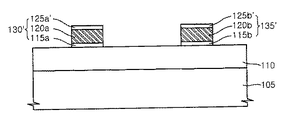
図3を参照すれば、バンプ170は、その下部のパッド電極膜130と電気的に連結される。パッド電極膜130及び整列マーク膜135は、半導体基板105上の層間絶縁膜110上に形成されうる。パッド電極膜130は、半導体基板105内または半導体基板105上の単位素子(図示せず)と電気的に連結され、これにより、単位素子に対する入出力端子の役割を行える。例えば、単位素子は、トランジスタまたはキャパシタ構造(図示せず)を含みうる。
Referring to FIG. 3, the
半導体素子は、半導体基板105上に形成され、単位素子と連結された複数の配線電極膜(図示せず)をさらに含みうる。例えば、層間絶縁膜110は、複数の絶縁膜の積層構造を含み、複数の配線電極膜は、複数の絶縁膜上にそれぞれ形成することもできる。この場合、パッド電極膜130は、配線電極膜のうち何れか一つ以上と電気的に連結されうる。例えば、層間絶縁膜110は、シリコン酸化膜またはシリコン窒化膜を含みうる。
The semiconductor element may further include a plurality of wiring electrode films (not shown) formed on the
例えば、パッド電極膜130及び整列マーク膜135は、同じ物質で形成されうる。さらに具体的には、例えば、パッド電極膜130は、障壁金属膜115a、配線金属膜120a及びキャッピング金属膜125aを含み、整列マーク膜135は、障壁金属膜115b、配線金属膜120b及びキャッピング金属膜125bを含みうる。障壁金属膜115a,115bは、層間絶縁膜110上に同じ物質でそれぞれ形成されうる。配線金属膜120a,120bは、障壁金属膜115a,115b上にそれぞれ同じ物質で形成されうる。キャッピング金属膜125a,125bは、配線金属膜120a,120b上にそれぞれ同じ物質で形成されうる。
For example, the
例えば、障壁金属膜115a,115bは、チタン膜、タンタル膜、チタン窒化膜、タンタル窒化膜、またはこれらが二つ以上積層された複合膜を含みうる。配線金属膜120a,120bは、電気抵抗の低いアルミニウム膜または銅膜を含みうる。キャッピング金属膜125a,125bは、チタン膜、タンタル膜、チタン窒化膜、タンタル窒化膜、またはこれらが二つ以上積層された複合膜を含みうる。キャッピング金属膜125a,125bは、配線金属膜120a,120bのパターニング時に反射防止膜として使うこともできる。
For example, the
キャッピング金属膜125a,125bは、配線金属膜120a,120bの少なくとも一部分122a,122bをそれぞれ露出するようにパターニングされうる。しかし、本発明の他の実施形態において、キャッピング金属膜125a,125bは、配線金属膜120a,120bの上部を覆っている。本発明のさらに他の実施形態において、パッド電極膜130及び整列マーク膜135は、複数の金属膜(図示せず)をさらに備えることもでき、または一つの金属膜で形成することもできる。
The capping
パッシベーション膜140は、層間絶縁膜110上に形成され、パッド電極膜130の上部の少なくとも一部分122a及び整列マーク膜135の上部の少なくとも一部分122bをそれぞれ露出できる。例えば、パッシベーション膜140は、ホール146,148を含み、ホール146によってパッド電極膜130の一部分122aが露出され、他のホール148によって整列マーク膜135の一部分122bが露出されうる。
The
さらに具体的には、ホール146,148は、キャッピング金属膜125a,125bの内部に拡張され、ホール146,148によって配線金属膜120a,120bがパッシベーション膜140及びキャッピング金属膜125a,125bから露出されうる。パッド電極膜130及び整列マーク膜135の側壁は、パッシベーション膜140によって取り囲まれうる。例えば、パッシベーション膜140は、シリコン窒化膜またはシリコン酸化膜を含みうる。パッシベーション膜140は、例えば、半導体基板105内または半導体基板105上の単位素子を水分から保護する役割を行える。
More specifically, the
透光性保護膜150は、パッシベーション膜140の少なくとも一部分を覆うように形成される。例えば、透光性保護膜150は、整列マーク膜135の上部の一部分122bを覆い、パッド電極膜130の上部の一部分122aを露出できる。さらに具体的には、例えば、透光性保護膜150は、ホール154を含み、ホール154によってパッド電極膜130の上部の一部分122a及びその周辺のパッシベーション膜140の一部分が露出されうる。
The translucent
透光性保護膜150は、その下部の半導体素子の構造を外部環境、例えば、物理的衝撃または水分のような化学的侵入から保護する役割を行える。例えば、透光性保護膜150は、感光性または非感光性ポリイミド膜、または透光性保護膜150は、シリコンゴム系列、エポキシ系列またはウレタン系列の絶縁膜をさらに備えることもできる。
The light-transmitting
パッシベーション膜140の厚さ変化は、整列マーク膜135の色相を変化させうる一方、透光性保護膜150の厚さ(d)変化は、上方から見た整列マーク膜135の色相をほとんど変化させない。これにより、透光性保護膜150の形成工程で、工程変化によってその厚さ(d)が変化されても、整列マーク膜135の色相は、一定に維持されうる。すなわち、フィールド領域と整列マーク膜135との色相差が一定に維持されうる。したがって、光整列装置は、透光性保護膜150の厚さ(d)が若干異なっても、半導体素子をエラーなしに整列させうる。
The change in the thickness of the
特に、キャッピング金属膜125bから配線金属膜120bの上部122bが露出された場合、フィールド領域と整列マーク膜135との色相差がかなり維持されうる。しかし、本発明の他の実施形態において、キャッピング金属膜125bが配線金属膜120bの上部122bを覆っていることも可能であり、この場合にも、フィールド領域と整列マーク膜135との色相差は、ある程度維持されうる。
In particular, when the
バンプ170は、パッシベーション膜140及び透光性保護膜150から露出されたパッド電極膜130の上部122aに形成される。例えば、バンプ170は、パッシベーション膜140のホール146を埋め込み、パッシベーション膜140上に所定幅ほど拡張され、透光性保護膜150上に延びうる。バンプ170は、配線金属膜120aの上部122aと直接接触されうる。しかし、本発明の他の実施形態において、バンプ170は、キャッピング金属膜125aと直接接触させることもできる。
The
例えば、透光性保護膜150上に露出されたバンプ170は、COG方式の組立工程でガラス基板との接続部位として利用されうる。バンプ170は、例えば、金(Au)膜を含みうる。バンプ170と配線金属膜120aの上部122aとの間、及びバンプ170とパッシベーション膜140との間には、第2障壁金属膜160が介在されうる。例えば、第2障壁金属膜160は、銅及びニッケルの合金膜を含み、第2障壁金属膜160と配線金属膜120aとの相互拡散を防止しうる。
For example, the
しかし、本発明の他の実施形態において、半導体素子がCOG方式で組立てられないならば、バンプ170は、省略されてもよい。例えば、他の導電性連結膜、例えば導電性ワイヤを利用してパッド電極膜130及び外部装置を連結することもできる。
However, in another embodiment of the present invention, the
[製造方法]
以下、図4ないし図11を参照して、本発明の実施形態による半導体素子の製造方法を説明する。
[Production method]
Hereinafter, a method of manufacturing a semiconductor device according to an embodiment of the present invention will be described with reference to FIGS.
図4を参照すれば、半導体基板105上に層間絶縁膜110を形成し、層間絶縁膜110上に予備パッド電極膜130’及び予備整列マーク膜135’を形成する。予備パッド電極膜130’及び予備整列マーク膜135’は、障壁金属膜115a,115b、配線金属膜120a,120b及び予備キャッピング金属膜125a’,125b’を含みうる。
Referring to FIG. 4, an
例えば、層間絶縁膜110上に障壁金属層(図示せず)、配線金属層(図示せず)及びキャッピング金属層(図示せず)を順次に形成する。次いで、通常のフォトリソグラフィ及びエッチング技術を利用して、障壁金属層、配線金属層及びキャッピング金属層をパターニングして、予備パッド電極膜130’及び予備整列マーク膜135’を同時に形成しうる。
For example, a barrier metal layer (not shown), a wiring metal layer (not shown), and a capping metal layer (not shown) are sequentially formed on the
図5を参照すれば、予備パッド電極膜130’及び予備整列マーク膜135’を覆うパッシベーション層140’を形成する。例えば、化学気相蒸着(Chemical Vapor Deposition:CVD)法を利用して、シリコン酸化膜またはシリコン窒化膜を備えるパッシベーション層140’を形成しうる。
Referring to FIG. 5, a passivation layer 140 'covering the preliminary pad electrode film 130' and the preliminary alignment mark film 135 'is formed. For example, the
次いで、パッシベーション層140’上に予備パッド電極膜130’及び予備整列マーク膜135’の一部分上のパッシベーション層140’を露出する第1フォトレジスト膜142を形成する。
Next, a
図6を参照すれば、第1フォトレジスト膜(図5の142)をエッチングマスクとして、パッシベーション層140’及びキャッピング金属膜125a,125bの露出された部分をエッチングしてホール146,148を備えるパッシベーション膜140を形成しうる。キャッピング金属膜125a,125bは、ホール146,148によって配線金属膜120a,120bの上部の一部分122a,122bをそれぞれ露出する。これにより、パッド電極膜130及び整列マーク膜135は、障壁金属膜115a,115b、配線金属膜120a,120b及びキャッピング金属膜125a,125bをそれぞれ含みうる。整列マーク膜135は、“+”型、“T”型、“L”型または反転した“L”型の平面構造を含みうる。
Referring to FIG. 6, the exposed portion of the
しかし、本発明の他の実施形態で、予備キャッピング金属膜(図5の125a’、125b’)はエッチングされず、配線金属膜120a,120bの上部を覆うことができる。この場合、配線金属膜130及び予備配線金属膜(図5の130’)は、互いに同じであり、整列マーク膜135及び予備整列マーク膜(図5の135’)は、互いに同じでありうる。
However, in another embodiment of the present invention, the preliminary capping metal films (125a 'and 125b' in FIG. 5) are not etched, and the upper portions of the
図7を参照すれば、パッシベーション膜140が形成された結果物上に透光性保護層150’を形成する。透光性保護層150’は、パッシベーション膜140のホール146,148を埋め込みうる。例えば、透光性保護層150’は、感光性または非感光性ポリイミド層、またはシリコンゴム系列、エポキシ系列またはウレタン系列絶縁層を含みうる。
Referring to FIG. 7, a translucent protective layer 150 'is formed on the resultant structure on which the
次いで、透光性保護層150’上に少なくとも配線金属膜120aの上部の一部分122a上の透光性保護層150’を露出する第2フォトレジスト膜152を形成する。
Next, a
図8を参照すれば、第2フォトレジスト膜(図7の152)をエッチングマスクとして、露出された透光性保護層(図7の150’)をエッチングし、透光性保護膜150を形成する。透光性保護膜150は、パッシベーション膜140のホール148を埋め込み、他のホール146を露出できる。すなわち、透光性保護膜150は、整列マーク膜135の配線金属膜120bの上部の一部分122bを覆い、パッド電極膜130の配線金属膜120aの上部の一部分122aを露出できる。透光性保護膜150は、ホール154を含み、ホール154は、パッシベーション膜140のホール146より大きい幅を有しうる。これにより、透光性保護膜150は、パッド電極膜130の周囲のパッシベーション膜140を露出できる。
Referring to FIG. 8, the exposed transparent protective layer (150 ′ of FIG. 7) is etched using the second photoresist film (152 of FIG. 7) as an etching mask to form the transparent
図9を参照すれば、透光性保護膜150が形成された結果物上に第2障壁金属層160’を形成する。例えば、第2障壁金属層160’は、ニッケル及び銅合金層を含み、通常の物質膜蒸着法を利用して形成されうる。
Referring to FIG. 9, a second
次いで、第2障壁金属層160’上に配線金属膜120aの上部の一部分122aを露出する第3フォトレジスト膜165を形成する。例えば、フォトレジスト膜165は、透光性保護膜150のホール154によって露出されたパッシベーション膜140の一部分を覆い、パッシベーション膜140のホール146を露出できる。これにより、配線金属膜120aの上部の一部分122a上の第2障壁金属層160’の一部分162が露出されうる。
Next, a
図10を参照すれば、第3フォトレジスト膜165によって露出された第2障壁金属層160’上にバンプ170を形成する。次いで、第3フォトレジスト膜165を除去する。例えば、バンプ170は、金(Au)膜を含み、メッキを利用して形成されうる。しかし、本発明の他の実施形態において、第2障壁金属層160’が省略され、バンプ170をパッド電極膜130上に形成することもできる。
Referring to FIG. 10, a
図11を参照すれば、バンプ170から露出された第2障壁金属層(図10の160’)を除去して第2障壁金属膜160を形成する。これにより、バンプ170と配線金属膜120aの上部の一部分122aとの間、及びバンプ170とパッシベーション膜140との間に第2障壁金属膜160が介在される。
Referring to FIG. 11, the second barrier metal layer 160 (160 'in FIG. 10) exposed from the
第2障壁金属層160’の一部分の除去工程の間に、透光性保護膜150は、整列マーク膜135を保護するエッチングマスクの役割を行える。もし、透光性保護膜150が整列マーク膜135を覆っていなければ、第2障壁金属層160’の一部分の除去工程は、さらに複雑な工程を経て進められるか、あるいは整列マーク膜135の一部分が損傷される恐れがある。しかし、本発明により、第2障壁金属層160’の一部分の除去工程が簡素化され、整列マーク膜135の一部分の損傷が防止されうる。
During the process of removing a portion of the second
[実験例]
表1は、本発明の実施形態による半導体素子及び従来の構造の半導体素子の整列特性を比較したものである。
[Experimental example]
Table 1 compares the alignment characteristics of a semiconductor device according to an embodiment of the present invention and a semiconductor device having a conventional structure.

グループI及びグループIIは、本発明の実施形態による半導体素子を表し、図3に示したように、半導体素子の整列マーク膜135上には、透光性保護膜150の例としてポリイミド膜が形成されている。グループIIIは、従来の半導体素子を表し、図1に示したように、整列マーク膜55上にパッシベーション膜60が形成されている。グループI及びグループIIは、ポリイミド膜の厚さを異ならせたものであり、グループIは、約3μmの厚さのポリイミド膜を有し、グループIIは、約3.8μmの厚さのポリイミド膜を有する。
Group I and Group II represent semiconductor devices according to embodiments of the present invention. As shown in FIG. 3, a polyimide film is formed on the
表1の結果を見れば、従来の半導体素子に対するグループIIIで、整列マーク膜135とフィールド領域との間の色相差を表すグレースケールの差値は、−29ないし−35(任意スケール)と比較的低くて広い範囲を有する。しかし、本発明の実施形態による半導体素子に対するグループI及びグループIIにおいて、グレースケールの差値は、53ないし55(任意スケール)とグループIIIより高くて均一であるということが分かる。
Referring to the results of Table 1, the gray scale difference value representing the hue difference between the
したがって、表1の結果から、第一に、本願発明による半導体素子の場合、従来よりもフィールド領域と整列マーク膜との間に高いグレースケールの差、すなわち、色相差を有するということが分かる。これにより、光整列装置で整列敏感度が高まりうる。第二に、本願発明による半導体素子の場合、ポリイミド膜の厚さが変化されてもグレースケールの差、すなわち、色相差がほとんどないということが分かる。したがって、ポリイミド膜の厚さが工程変化を有するとしても、半導体素子がエラーなしに整列されうる。 Therefore, from the results of Table 1, it can be seen that, firstly, the semiconductor device according to the present invention has a higher gray scale difference, that is, a hue difference between the field region and the alignment mark film than in the prior art. Thereby, the alignment sensitivity can be increased in the optical alignment device. Second, in the case of the semiconductor element according to the present invention, it can be seen that there is almost no difference in gray scale, that is, a hue difference even if the thickness of the polyimide film is changed. Therefore, even if the thickness of the polyimide film has a process change, the semiconductor elements can be aligned without error.
本発明の特定実施形態についての以上の説明は、例示及び説明を目的として提供された。したがって、本発明は、前記実施形態に限定されず、本発明の技術的思想内で当業者によって前記実施形態を組み合わせて実施するなど、多様な修正及び変更が可能であるということは明白である。 The foregoing descriptions of specific embodiments of the present invention have been presented for purposes of illustration and description. Therefore, the present invention is not limited to the above-described embodiment, and it is obvious that various modifications and changes can be made, for example, a combination of the above-described embodiments by a person skilled in the art within the technical idea of the present invention. .
本発明は、半導体素子関連の技術分野に適用可能である。 The present invention is applicable to a technical field related to semiconductor elements.
105 半導体基板
110 層間絶縁膜
130 パッド電極膜
135 整列マーク膜
140 パッシベーション膜
150 透光性保護膜
160 第2障壁金属膜
170 バンプ
105
Claims (22)
前記半導体基板上に形成され、組立工程の整列キーとして利用される整列マーク膜と、
前記半導体基板上に形成され、前記パッド電極膜の上部の少なくとも一部分及び前記整列マーク膜の上部の少なくとも一部分をそれぞれ露出するパッシベーション膜と、
前記パッシベーション膜の少なくとも一部分を覆い、前記パッシベーション膜から露出された前記パッド電極膜の上部を露出し、前記パッシベーション膜から露出された前記整列マーク膜を覆っている透光性保護膜と、を備えることを特徴とする半導体素子。 A pad electrode film on a semiconductor substrate;
An alignment mark film formed on the semiconductor substrate and used as an alignment key in an assembly process;
A passivation film formed on the semiconductor substrate and exposing at least part of the upper part of the pad electrode film and at least part of the upper part of the alignment mark film;
A translucent protective film that covers at least a part of the passivation film, exposes an upper portion of the pad electrode film exposed from the passivation film, and covers the alignment mark film exposed from the passivation film. The semiconductor element characterized by the above-mentioned.
前記層間絶縁膜上に形成されたパッド電極膜と、
前記層間絶縁膜上に形成され、組立工程の整列キーとして利用される整列マーク膜と、
前記層間絶縁膜上に形成され、前記パッド電極膜の上部の少なくとも一部分及び前記整列マーク膜の上部の少なくとも一部分をそれぞれ露出するパッシベーション膜と、
前記パッシベーション膜の少なくとも一部分を覆い、前記パッシベーション膜から露出された前記パッド電極膜の上部を露出し、前記パッシベーション膜から露出された前記整列マーク膜を覆っているポリイミド膜と、
前記パッシベーション膜及びポリイミド膜から露出された前記パッド電極膜上のバンプと、を備えることを特徴とする半導体素子。 An interlayer insulating film on the semiconductor substrate;
A pad electrode film formed on the interlayer insulating film;
An alignment mark film formed on the interlayer insulating film and used as an alignment key in an assembly process;
A passivation film formed on the interlayer insulating film and exposing at least part of the upper part of the pad electrode film and at least part of the upper part of the alignment mark film;
A polyimide film covering at least a portion of the passivation film, exposing an upper portion of the pad electrode film exposed from the passivation film, and covering the alignment mark film exposed from the passivation film;
And a bump on the pad electrode film exposed from the passivation film and the polyimide film.
前記半導体基板上に前記パッド電極膜の上部の少なくとも一部分及び前記整列マーク膜の上部の少なくとも一部分をそれぞれ露出するパッシベーション膜を形成する工程と、
前記パッシベーション膜が形成された結果物上に、前記パッシベーション膜から露出された前記パッド電極膜の上部を露出し、前記パッシベーション膜から露出された前記整列マーク膜を覆っている透光性保護膜を形成する工程と、を含むことを特徴とする半導体素子の製造方法。 Forming a pad electrode film and an alignment mark film used as an alignment key for an assembly process on a semiconductor substrate;
Forming a passivation film on the semiconductor substrate to expose at least part of the upper part of the pad electrode film and at least part of the upper part of the alignment mark film;
A translucent protective film that exposes an upper portion of the pad electrode film exposed from the passivation film and covers the alignment mark film exposed from the passivation film is formed on the resultant product on which the passivation film is formed. Forming the semiconductor element.
前記半導体基板上に障壁金属層を形成する工程と、
前記障壁金属層上に配線金属層を形成する工程と、
前記配線金属層上にキャッピング金属層を形成する工程と、
前記障壁金属層、前記配線金属層及び前記キャッピング金属層をパターニングして、前記障壁金属膜、配線金属膜及びキャッピング金属膜を備えるパッド電極膜を形成すると同時に、前記障壁金属膜、配線金属膜及びキャッピング金属膜を備える整列マーク膜を形成する工程と、を含むことを特徴とする請求項15に記載の半導体素子の製造方法。 Forming the pad electrode film and the alignment mark film;
Forming a barrier metal layer on the semiconductor substrate;
Forming a wiring metal layer on the barrier metal layer;
Forming a capping metal layer on the wiring metal layer;
The barrier metal layer, the wiring metal layer, and the capping metal layer are patterned to form a pad electrode film including the barrier metal film, the wiring metal film, and the capping metal film, and at the same time, the barrier metal film, the wiring metal film, and The method of manufacturing a semiconductor device according to claim 15, further comprising: forming an alignment mark film including a capping metal film.
前記第2障壁金属層上に、少なくとも前記透光性保護膜から露出された前記パッド電極膜上の前記第2障壁金属層を露出するマスク膜を形成する工程と、
前記マスク膜から露出された前記第2障壁金属層上にバンプを形成する工程と、
前記マスク膜を除去する工程と、
前記バンプから露出された前記第2障壁金属層をエッチングして第2障壁金属膜を形成する工程と、をさらに含むことを特徴とする請求項15に記載の半導体素子の製造方法。 Forming a second barrier metal layer on the resultant structure on which the translucent protective film is formed;
Forming a mask film on the second barrier metal layer to expose the second barrier metal layer on at least the pad electrode film exposed from the translucent protective film;
Forming bumps on the second barrier metal layer exposed from the mask film;
Removing the mask film;
The method of claim 15, further comprising: etching the second barrier metal layer exposed from the bump to form a second barrier metal film.
Applications Claiming Priority (1)
| Application Number | Priority Date | Filing Date | Title |
|---|---|---|---|
| KR1020050111994A KR100660893B1 (en) | 2005-11-22 | 2005-11-22 | Semiconductor device having a align mark film and method of fabricating the same |
Publications (2)
| Publication Number | Publication Date |
|---|---|
| JP2007142436A true JP2007142436A (en) | 2007-06-07 |
| JP2007142436A5 JP2007142436A5 (en) | 2010-01-14 |
Family
ID=37815395
Family Applications (1)
| Application Number | Title | Priority Date | Filing Date |
|---|---|---|---|
| JP2006313358A Pending JP2007142436A (en) | 2005-11-22 | 2006-11-20 | Semiconductor device comprising lineup mark film and method of manufacturing same |
Country Status (5)
| Country | Link |
|---|---|
| US (1) | US7482703B2 (en) |
| JP (1) | JP2007142436A (en) |
| KR (1) | KR100660893B1 (en) |
| CN (1) | CN1971903B (en) |
| DE (1) | DE102006056066A1 (en) |
Cited By (4)
| Publication number | Priority date | Publication date | Assignee | Title |
|---|---|---|---|---|
| JP2010225934A (en) * | 2009-03-24 | 2010-10-07 | Mitsumi Electric Co Ltd | Method of manufacturing wafer |
| CN102157497A (en) * | 2011-01-26 | 2011-08-17 | 上海宏力半导体制造有限公司 | Multi-layer stacked semiconductor device structure and forming method |
| US8274166B2 (en) | 2008-07-09 | 2012-09-25 | Renesas Electronics Corporation | Semiconductor device and method of manufacturing the same |
| KR101345393B1 (en) | 2011-03-16 | 2013-12-24 | 글로벌파운드리즈 드레스덴 모듈 원 리미티드 라이어빌리티 컴퍼니 & 씨오. 케이지 | Protection of reactive metal surfaces of semiconductor devices during shipping by providing an additional protection layer |
Families Citing this family (21)
| Publication number | Priority date | Publication date | Assignee | Title |
|---|---|---|---|---|
| US8492263B2 (en) * | 2007-11-16 | 2013-07-23 | Taiwan Semiconductor Manufacturing Company, Ltd. | Protected solder ball joints in wafer level chip-scale packaging |
| US20090174069A1 (en) * | 2008-01-04 | 2009-07-09 | National Semiconductor Corporation | I/o pad structure for enhancing solder joint reliability in integrated circuit devices |
| KR20090095076A (en) * | 2008-03-04 | 2009-09-09 | 삼성전자주식회사 | Semiconductor integrated circuit device and method of fabricating the same |
| CN101789391B (en) * | 2009-01-23 | 2012-08-22 | 中芯国际集成电路制造(上海)有限公司 | Semiconductor device and manufacturing method thereof |
| US8299616B2 (en) * | 2010-01-29 | 2012-10-30 | Taiwan Semiconductor Manufacturing Company, Ltd. | T-shaped post for semiconductor devices |
| US8318596B2 (en) | 2010-02-11 | 2012-11-27 | Taiwan Semiconductor Manufacturing Company, Ltd. | Pillar structure having a non-planar surface for semiconductor devices |
| US8803319B2 (en) | 2010-02-11 | 2014-08-12 | Taiwan Semiconductor Manufacturing Company, Ltd. | Pillar structure having a non-planar surface for semiconductor devices |
| JP2013004572A (en) * | 2011-06-13 | 2013-01-07 | Mitsubishi Electric Corp | Semiconductor device manufacturing method |
| US9230932B2 (en) | 2012-02-09 | 2016-01-05 | Taiwan Semiconductor Manufacturing Company, Ltd. | Interconnect crack arrestor structure and methods |
| US9515036B2 (en) | 2012-04-20 | 2016-12-06 | Taiwan Semiconductor Manufacturing Company, Ltd. | Methods and apparatus for solder connections |
| CN103682085B (en) * | 2012-09-20 | 2016-08-03 | 中芯国际集成电路制造(上海)有限公司 | A kind of MAGNETIC RANDOM ACCESS MEMORY and manufacture method thereof |
| CN103199084B (en) * | 2013-03-08 | 2015-10-14 | 京东方科技集团股份有限公司 | The manufacture method of substrate alignment mark, substrate and substrate alignment mark |
| US8987922B2 (en) | 2013-03-11 | 2015-03-24 | Taiwan Semiconductor Manufacturing Company, Ltd. | Methods and apparatus for wafer level packaging |
| US9355979B2 (en) * | 2013-08-16 | 2016-05-31 | Taiwan Semiconductor Manufacturing Company, Ltd. | Alignment structures and methods of forming same |
| CN104091808B (en) * | 2014-06-25 | 2016-08-17 | 合肥鑫晟光电科技有限公司 | Array base palte and preparation method thereof and display device |
| US9505609B2 (en) * | 2015-04-29 | 2016-11-29 | Invensense, Inc. | CMOS-MEMS integrated device with selective bond pad protection |
| US9935047B2 (en) | 2015-10-16 | 2018-04-03 | Taiwan Semiconductor Manufacturing Company, Ltd. | Bonding structures and methods forming the same |
| US10658318B2 (en) * | 2016-11-29 | 2020-05-19 | Taiwan Semiconductor Manufacturing Co., Ltd. | Film scheme for bumping |
| KR101902566B1 (en) * | 2017-07-25 | 2018-09-28 | 엘지디스플레이 주식회사 | Light emitting diode display apparatus and manufacturing method of the same |
| US11694967B2 (en) * | 2019-03-14 | 2023-07-04 | Taiwan Semiconductor Manufacturing Company, Ltd. | Package structure and method of fabricating the same |
| CN114093842A (en) * | 2020-12-23 | 2022-02-25 | 矽磐微电子(重庆)有限公司 | Bare chip and manufacturing method thereof, chip packaging structure and manufacturing method thereof |
Citations (7)
| Publication number | Priority date | Publication date | Assignee | Title |
|---|---|---|---|---|
| JPH03105937A (en) * | 1989-09-19 | 1991-05-02 | Nec Corp | Semiconductor device |
| JPH0590325A (en) * | 1991-09-27 | 1993-04-09 | Toshiba Corp | Bonding of semiconductor device |
| JPH08152646A (en) * | 1994-11-28 | 1996-06-11 | Canon Inc | Circuit board structure and positioning device for manufacturing circuit board structure |
| JP2002500440A (en) * | 1997-12-31 | 2002-01-08 | インテル・コーポレーション | Wafer passivation structure and manufacturing method |
| JP2004319549A (en) * | 2003-04-11 | 2004-11-11 | Matsushita Electric Ind Co Ltd | Semiconductor device and its manufacturing method |
| JP2005044971A (en) * | 2003-07-28 | 2005-02-17 | Sharp Corp | Semiconductor device and its manufacturing method |
| JP2005109145A (en) * | 2003-09-30 | 2005-04-21 | Toshiba Corp | Semiconductor device |
Family Cites Families (10)
| Publication number | Priority date | Publication date | Assignee | Title |
|---|---|---|---|---|
| JPH0488622A (en) * | 1990-08-01 | 1992-03-23 | Fujitsu Ltd | Manufacture of semiconductor device |
| KR100258719B1 (en) | 1993-04-16 | 2000-06-15 | 손욱 | Pannel structure for chip on glass(cog) |
| KR960008978A (en) * | 1994-08-02 | 1996-03-22 | 김주용 | Alignment mark protection method of semiconductor device |
| JP4037561B2 (en) * | 1999-06-28 | 2008-01-23 | 株式会社東芝 | Manufacturing method of semiconductor device |
| US6586323B1 (en) * | 2000-09-18 | 2003-07-01 | Taiwan Semiconductor Manufacturing Company | Method for dual-layer polyimide processing on bumping technology |
| US6465898B1 (en) * | 2001-07-23 | 2002-10-15 | Texas Instruments Incorporated | Bonding alignment mark for bonds over active circuits |
| JP2005012065A (en) * | 2003-06-20 | 2005-01-13 | Renesas Technology Corp | Semiconductor device and its manufacturing method |
| US7122458B2 (en) * | 2004-07-22 | 2006-10-17 | Taiwan Semiconductor Manufacturing Co., Ltd. | Method for fabricating pad redistribution layer |
| KR100577308B1 (en) * | 2004-12-29 | 2006-05-10 | 동부일렉트로닉스 주식회사 | Semiconductor device and method for manufacturing the same |
| KR100712289B1 (en) * | 2005-04-07 | 2007-04-27 | 삼성에스디아이 주식회사 | Flat Panel Display and Fabrication Method of the Same |
-
2005
- 2005-11-22 KR KR1020050111994A patent/KR100660893B1/en not_active IP Right Cessation
-
2006
- 2006-06-23 US US11/473,852 patent/US7482703B2/en active Active
- 2006-11-20 DE DE102006056066A patent/DE102006056066A1/en not_active Withdrawn
- 2006-11-20 JP JP2006313358A patent/JP2007142436A/en active Pending
- 2006-11-22 CN CN2006101486633A patent/CN1971903B/en active Active
Patent Citations (7)
| Publication number | Priority date | Publication date | Assignee | Title |
|---|---|---|---|---|
| JPH03105937A (en) * | 1989-09-19 | 1991-05-02 | Nec Corp | Semiconductor device |
| JPH0590325A (en) * | 1991-09-27 | 1993-04-09 | Toshiba Corp | Bonding of semiconductor device |
| JPH08152646A (en) * | 1994-11-28 | 1996-06-11 | Canon Inc | Circuit board structure and positioning device for manufacturing circuit board structure |
| JP2002500440A (en) * | 1997-12-31 | 2002-01-08 | インテル・コーポレーション | Wafer passivation structure and manufacturing method |
| JP2004319549A (en) * | 2003-04-11 | 2004-11-11 | Matsushita Electric Ind Co Ltd | Semiconductor device and its manufacturing method |
| JP2005044971A (en) * | 2003-07-28 | 2005-02-17 | Sharp Corp | Semiconductor device and its manufacturing method |
| JP2005109145A (en) * | 2003-09-30 | 2005-04-21 | Toshiba Corp | Semiconductor device |
Cited By (5)
| Publication number | Priority date | Publication date | Assignee | Title |
|---|---|---|---|---|
| US8274166B2 (en) | 2008-07-09 | 2012-09-25 | Renesas Electronics Corporation | Semiconductor device and method of manufacturing the same |
| JP2010225934A (en) * | 2009-03-24 | 2010-10-07 | Mitsumi Electric Co Ltd | Method of manufacturing wafer |
| CN102157497A (en) * | 2011-01-26 | 2011-08-17 | 上海宏力半导体制造有限公司 | Multi-layer stacked semiconductor device structure and forming method |
| CN102157497B (en) * | 2011-01-26 | 2016-03-09 | 上海华虹宏力半导体制造有限公司 | The structure of the semiconductor device of Multilayer stack and formation method |
| KR101345393B1 (en) | 2011-03-16 | 2013-12-24 | 글로벌파운드리즈 드레스덴 모듈 원 리미티드 라이어빌리티 컴퍼니 & 씨오. 케이지 | Protection of reactive metal surfaces of semiconductor devices during shipping by providing an additional protection layer |
Also Published As
| Publication number | Publication date |
|---|---|
| CN1971903A (en) | 2007-05-30 |
| US7482703B2 (en) | 2009-01-27 |
| DE102006056066A1 (en) | 2007-06-14 |
| CN1971903B (en) | 2010-05-19 |
| US20070117343A1 (en) | 2007-05-24 |
| KR100660893B1 (en) | 2006-12-26 |
Similar Documents
| Publication | Publication Date | Title |
|---|---|---|
| JP2007142436A (en) | Semiconductor device comprising lineup mark film and method of manufacturing same | |
| US20190148653A1 (en) | Flexible display substrate and method for manufacturing the same, and flexible display device | |
| KR100867866B1 (en) | Tft matrix structure and manufacturing method thereof | |
| US8563980B2 (en) | Array substrate and manufacturing method | |
| US7045908B2 (en) | Semiconductor device and method for manufacturing the same | |
| US7880256B2 (en) | Semiconductor device with passivation layer covering wiring layer | |
| JP4544860B2 (en) | Method of manufacturing contact portion of semiconductor element, and method of manufacturing thin film transistor array substrate for liquid crystal display device including the same | |
| JP2003195355A (en) | Contact portion of semiconductor device and method for manufacturing the same and thin film transistor array panel for displaying device including the contact portion and method for manufacturing the same | |
| JP2002026333A (en) | Method of manufacturing active matrix board | |
| JP2004163933A (en) | Array substrate for liquid crystal display device and method of manufacturing the same | |
| KR100558714B1 (en) | Liquid crystal display and fabricating method thereof | |
| JP2009122244A (en) | Method of manufacturing thin film transistor array substrate, and display device | |
| KR100807580B1 (en) | Fabricating method of liquid crystal display | |
| US8471993B2 (en) | Common line structure and display panel and method of making the same | |
| US8288212B2 (en) | Pixel structure of a thin film transistor liquid crystal display and fabricating method thereof | |
| US8648442B2 (en) | Semiconductor device and method of manufacturing the same | |
| US20060057831A1 (en) | Wire bond pads | |
| JP2006293376A (en) | Phase shift mask | |
| TWI754323B (en) | Device array substrate and manufacturing method thereof | |
| KR100750920B1 (en) | A manufacturing method of a thin film transistor array panel | |
| CN112909018B (en) | Element array substrate and manufacturing method thereof | |
| KR100840322B1 (en) | A manufacturing method of liquid crystal display | |
| US6781644B1 (en) | Liquid crystal display with thin film transistor array free from short-circuit and process for fabrication thereof | |
| KR102156346B1 (en) | Method of fabricating array substrate for fringe field switching mode liquid crystal display device | |
| KR100309921B1 (en) | Liquid crystal display and a manufacturing method thereof |
Legal Events
| Date | Code | Title | Description |
|---|---|---|---|
| A521 | Written amendment |
Free format text: JAPANESE INTERMEDIATE CODE: A523 Effective date: 20091119 |
|
| A621 | Written request for application examination |
Free format text: JAPANESE INTERMEDIATE CODE: A621 Effective date: 20091119 |
|
| A521 | Written amendment |
Free format text: JAPANESE INTERMEDIATE CODE: A523 Effective date: 20101026 |
|
| A131 | Notification of reasons for refusal |
Free format text: JAPANESE INTERMEDIATE CODE: A131 Effective date: 20121016 |
|
| A02 | Decision of refusal |
Free format text: JAPANESE INTERMEDIATE CODE: A02 Effective date: 20130402 |