JP2007123768A - Thin film capacitor and its manufacturing method - Google Patents
Thin film capacitor and its manufacturing method Download PDFInfo
- Publication number
- JP2007123768A JP2007123768A JP2005317416A JP2005317416A JP2007123768A JP 2007123768 A JP2007123768 A JP 2007123768A JP 2005317416 A JP2005317416 A JP 2005317416A JP 2005317416 A JP2005317416 A JP 2005317416A JP 2007123768 A JP2007123768 A JP 2007123768A
- Authority
- JP
- Japan
- Prior art keywords
- taper
- thin film
- film capacitor
- upper electrode
- dielectric layer
- Prior art date
- Legal status (The legal status is an assumption and is not a legal conclusion. Google has not performed a legal analysis and makes no representation as to the accuracy of the status listed.)
- Withdrawn
Links
- 239000003990 capacitor Substances 0.000 title claims abstract description 31
- 238000004519 manufacturing process Methods 0.000 title claims abstract description 21
- 239000010409 thin film Substances 0.000 title claims abstract description 21
- 239000000463 material Substances 0.000 claims description 13
- 238000005530 etching Methods 0.000 claims description 8
- 238000001312 dry etching Methods 0.000 claims description 6
- 230000009467 reduction Effects 0.000 abstract description 4
- 230000015556 catabolic process Effects 0.000 abstract description 2
- 239000010410 layer Substances 0.000 description 36
- 238000000151 deposition Methods 0.000 description 21
- 230000008021 deposition Effects 0.000 description 21
- 238000000034 method Methods 0.000 description 16
- 239000010408 film Substances 0.000 description 12
- 230000001681 protective effect Effects 0.000 description 9
- 229910052751 metal Inorganic materials 0.000 description 8
- 239000002184 metal Substances 0.000 description 8
- 239000000758 substrate Substances 0.000 description 7
- 230000007547 defect Effects 0.000 description 6
- 230000006866 deterioration Effects 0.000 description 5
- 150000002500 ions Chemical class 0.000 description 5
- 230000007423 decrease Effects 0.000 description 4
- 238000000605 extraction Methods 0.000 description 4
- 238000009616 inductively coupled plasma Methods 0.000 description 4
- 239000004065 semiconductor Substances 0.000 description 4
- 230000000694 effects Effects 0.000 description 3
- 230000006872 improvement Effects 0.000 description 3
- 230000008569 process Effects 0.000 description 3
- 229920005989 resin Polymers 0.000 description 3
- 239000011347 resin Substances 0.000 description 3
- 238000001039 wet etching Methods 0.000 description 3
- 240000007711 Peperomia pellucida Species 0.000 description 2
- 230000015572 biosynthetic process Effects 0.000 description 2
- URQUNWYOBNUYJQ-UHFFFAOYSA-N diazonaphthoquinone Chemical compound C1=CC=C2C(=O)C(=[N]=[N])C=CC2=C1 URQUNWYOBNUYJQ-UHFFFAOYSA-N 0.000 description 2
- 230000005684 electric field Effects 0.000 description 2
- 229920003986 novolac Polymers 0.000 description 2
- 229920002120 photoresistant polymer Polymers 0.000 description 2
- 239000011148 porous material Substances 0.000 description 2
- 238000004528 spin coating Methods 0.000 description 2
- QVGXLLKOCUKJST-UHFFFAOYSA-N atomic oxygen Chemical compound [O] QVGXLLKOCUKJST-UHFFFAOYSA-N 0.000 description 1
- 239000003985 ceramic capacitor Substances 0.000 description 1
- 230000008859 change Effects 0.000 description 1
- 230000002860 competitive effect Effects 0.000 description 1
- 230000002950 deficient Effects 0.000 description 1
- 238000005516 engineering process Methods 0.000 description 1
- 230000007613 environmental effect Effects 0.000 description 1
- 239000007789 gas Substances 0.000 description 1
- 230000009477 glass transition Effects 0.000 description 1
- 238000010438 heat treatment Methods 0.000 description 1
- 230000010354 integration Effects 0.000 description 1
- 238000004377 microelectronic Methods 0.000 description 1
- 238000012986 modification Methods 0.000 description 1
- 230000004048 modification Effects 0.000 description 1
- 229910000510 noble metal Inorganic materials 0.000 description 1
- 239000001301 oxygen Substances 0.000 description 1
- 229910052760 oxygen Inorganic materials 0.000 description 1
- 239000002245 particle Substances 0.000 description 1
- 239000002356 single layer Substances 0.000 description 1
- 241000894007 species Species 0.000 description 1
Images
Landscapes
- Fixed Capacitors And Capacitor Manufacturing Machines (AREA)
- Semiconductor Integrated Circuits (AREA)
Abstract
Description
本発明は、誘電体を金属電極で挟んだMIM型の薄膜コンデンサ(キャパシタ)及びその製造方法に関し、特に、その製造歩留まりや信頼性の向上に関するものである。 The present invention relates to an MIM type thin film capacitor (capacitor) in which a dielectric is sandwiched between metal electrodes and a method for manufacturing the same, and more particularly to an improvement in manufacturing yield and reliability.
キャパシタとしては積層セラミックコンデンサ(MLCC)が主流であるが、昨今の高周波化が進む中では、そのインダクタンス成分,具体的には電極構造に由来するESL(等価直列インダクタンス)が問題となる。このESLを低くするため、高周波領域におけるキャパシタは、電極に流れる電流によって発生する磁場を低下させる構造を持ったIDCタイプにシフトしてきている。しかし、昨今の更なる高周波化の進行に伴い、現状のIDCタイプのキャパシタよりも更なる低ESLが要求されるに至っており、TH(Through Hole)タイプの薄膜コンデンサの検討が行われ始めてきている。 As a capacitor, a multilayer ceramic capacitor (MLCC) is the mainstream. However, with the recent increase in frequency, the inductance component, specifically, ESL (equivalent series inductance) derived from the electrode structure becomes a problem. In order to lower the ESL, capacitors in the high frequency region have been shifted to IDC types having a structure that reduces the magnetic field generated by the current flowing through the electrodes. However, with the recent progress of higher frequency, a further lower ESL is required than the current IDC type capacitor, and TH (Through Hole) type thin film capacitors are being studied. Yes.
ところで、薄膜コンデンサの製造歩留まりや信頼性には、加工技術が大きく関係している。薄膜の加工技術はドライエッチング法とウエットエッチング法に大別されるが、従来のウエットエッチング法では、電極として用いられる貴金属の安定性のために生ずる加工困難性の他に、プロセス中に発生するパーティクルや溶液の環境負荷への適応困難性,加工が等方的であることに対する適応困難性などの不都合がある。 By the way, processing technology is greatly related to the manufacturing yield and reliability of thin film capacitors. Thin film processing techniques are broadly divided into dry etching methods and wet etching methods. In conventional wet etching methods, in addition to processing difficulties caused by the stability of noble metals used as electrodes, they occur during the process. There are inconveniences such as difficulty in adapting to the environmental load of particles and solutions, and difficulty in adapting to isotropic processing.
これに対し、ドライエッチング法,例えばICP(高密度誘導結合プラズマ)を使用する方法では、上述したウエットエッチング法における問題点を改善できる可能性がある。しかしながら、従来の半導体デバイス(半導体集積回路)の構造では、
a,加工時に発生する金属残渣のデポジション(加工端面への削りカスの付着),
b,ラビットイヤー(加工残渣のレジスト表面への付着起こり、レジスト除去後に端面にウサギの耳のような被加工物の残渣が残る現象),
c,エッジ部位に絶縁膜塗布の際に発生するポアや熱膨張係数の差異によるクラック,
などにより、製造歩留まりの低下や、耐圧性の劣化などの信頼性の低下を招く恐れがある。
On the other hand, in the dry etching method, for example, the method using ICP (High Density Inductively Coupled Plasma), there is a possibility that the above-mentioned problems in the wet etching method can be improved. However, in the structure of a conventional semiconductor device (semiconductor integrated circuit),
a, Deposition of metal residue generated during processing (attachment of shavings to processing end face),
b, rabbit ear (a phenomenon in which processing residue adheres to the resist surface, and a residue of a workpiece such as a rabbit ear remains on the end surface after resist removal),
c, cracks caused by differences in pores and thermal expansion coefficients generated when an insulating film is applied to the edge part,
As a result, there is a risk of lowering the manufacturing yield or lowering reliability such as deterioration of pressure resistance.
具体的に説明すると、従来の半導体デバイスでは、高性能化と高集積化が密接に関連しているために、加工形状(テーパ角)は比較的垂直形状に近い構造となっている。しかし、このような垂直構造を、薄膜のMIMキャパシタにおける上部電極及び誘電体層の2層加工に適応すると、ドライエッチングにより発生した下部電極のオーバーエッチングなどに由来する金属残渣の付着レートが、ドライエッチングのエッチングレートより大きくなってしまう。このため、加工面に金属残渣が形成され、製造歩留まりの悪化につながる可能性がある。このような現象については、下記非特許文献1にも記載されており、ごく一般的である。 Specifically, in the conventional semiconductor device, since the high performance and the high integration are closely related, the processing shape (taper angle) has a structure close to a vertical shape. However, when such a vertical structure is applied to the two-layer processing of the upper electrode and the dielectric layer in the thin film MIM capacitor, the adhesion rate of the metal residue derived from the over-etching of the lower electrode caused by the dry etching is reduced. It becomes larger than the etching rate of etching. For this reason, metal residues are formed on the processed surface, which may lead to a deterioration in manufacturing yield. Such a phenomenon is described in Non-Patent Document 1 below, and is very common.
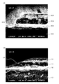
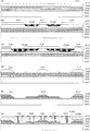
図4(A)には、その一例が示されており、基板900上に、下部電極902,誘電体層904,上部電極906が順に積層形成されている。図中の左側が上述した比較的テーパ角度が大きい形状となっているため、金属残渣のデポジション908が生じている。
FIG. 4A shows an example, in which a
このような不都合の解決策として、レジスト形状を低角度にコントロールする技術が、下記非特許文献2に報告されている。しかし、レジスト形状をコントロールする方法については、最終的なテーパ形状より微小線幅が優先される傾向にあり、前記非特許文献2に報告されている加工形状は、比較的大きなテーパ角となっている。
このように、MIMコンデンサの薄膜化に伴い、垂直もしくはそれに近い端面加工形状では、わずかなデポジションによっても電気特性の悪化につながってしまう可能性が高くなる。また、コンデンサ加工後に行なわれる絶縁膜等の保護膜の形成においては、垂直形状もしくはそれに近い形状では、保護膜形成の際に端面部位に空気をまきこみ、ポアが発生したり、基板・絶縁膜間の熱膨張係数の差から熱処理中にクラックが発生する可能性がある。これらの現象は、いずれもMIMコンデンサのリーク特性の悪化による信頼性の低下や、製造歩留まりの悪化などの原因となる。 As described above, as the thickness of the MIM capacitor is reduced, there is a high possibility that electrical characteristics will be deteriorated even by slight deposition in the vertical or near end face processed shape. In addition, when forming a protective film such as an insulating film after capacitor processing, if the shape is vertical or close to it, air may be trapped in the end surface when forming the protective film, causing pores, or between the substrate and the insulating film. Cracks may occur during heat treatment due to the difference in thermal expansion coefficient. Both of these phenomena cause a decrease in reliability due to deterioration of the leakage characteristics of the MIM capacitor and a decrease in manufacturing yield.
本発明は、以上の点に着目したもので、リーク特性の悪化による信頼性の低下を防ぎ、製造歩留まりの向上を図ることができる薄膜コンデンサ及びその製造方法を提供することを、その目的とするものである。 The present invention focuses on the above points, and an object of the present invention is to provide a thin film capacitor capable of preventing a decrease in reliability due to deterioration of leakage characteristics and improving a manufacturing yield and a manufacturing method thereof. Is.
前記目的を達成するため、本発明は、下部電極,誘電体層,上部電極を積層したMIM型の薄膜コンデンサであって、少なくとも前記誘電体層及び上部電極の端部にテーパを形成するとともに、前記テーパの角度を40°以下としたことを特徴とする。本発明の主要な形態の一つは、前記テーパの角度を30°以下,好ましくは23°以下としたことを特徴とする。 In order to achieve the above object, the present invention is a MIM type thin film capacitor in which a lower electrode, a dielectric layer, and an upper electrode are laminated, and at least ends of the dielectric layer and the upper electrode are tapered, The taper angle is 40 ° or less. One of the main aspects of the present invention is characterized in that the taper angle is 30 ° or less, preferably 23 ° or less.
他の発明は、前記薄膜コンデンサの製造方法であって、ドライエッチングによって前記テーパを形成する際に、レジスト材料に形成するテーパの調整,露光条件の調整,レジスト材料のベーク温度の調整,エッチングレートの材料間の選択比の調整の少なくとも一つにより、前記テーパの角度を調整することを特徴とする。本発明の前記及び他の目的,特徴,利点は、以下の詳細な説明及び添付図面から明瞭になろう。 Another invention is a method of manufacturing the thin film capacitor, wherein when the taper is formed by dry etching, adjustment of the taper formed on the resist material, adjustment of exposure conditions, adjustment of the baking temperature of the resist material, etching rate The taper angle is adjusted by at least one of adjustment of the selection ratio between the materials. The above and other objects, features and advantages of the present invention will become apparent from the following detailed description and the accompanying drawings.
本発明によれば、少なくとも上部電極と誘電体層の端部にテーパを設けることで、端部の断面積が拡大(例えば1.5倍以上)して電界の集中が緩和され、電圧破壊による故障が低減される。このため、製造歩留まりや信頼性が向上する。 According to the present invention, by providing a taper at least at the end portions of the upper electrode and the dielectric layer, the cross-sectional area of the end portions is enlarged (for example, 1.5 times or more), and the concentration of the electric field is alleviated. Failure is reduced. For this reason, manufacturing yield and reliability are improved.
以下、本発明を実施するための最良の形態を、実施例に基づいて詳細に説明する。 Hereinafter, the best mode for carrying out the present invention will be described in detail based on examples.
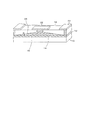
最初に、図1を参照しながら、本実施例の薄膜コンデンサの構成について説明する。図1に示すように、適宜の基板10の主面上に、下部電極12,誘電体層14,上部電極16が順に積層形成されており、更にその上に保護膜18が形成されている。下部電極12,誘電体層14,上部電極16によって、MIM構造が形成されている。下部電極12は、保護膜18を貫通して引出電極20に接続されており、上部電極16は、保護膜18を貫通して引出電極22に接続されている。
First, the configuration of the thin film capacitor of this example will be described with reference to FIG. As shown in FIG. 1, a
ところで、本実施例では、図1に示すように、誘電体層14及び上部電極16の端部ないし端面に、上部電極16の中心部から下部電極12の端部に向かって下降するテーパ24が形成されている。テーパ24の傾斜角度αは、40°以下,好ましくは30°以下に設定される。このように、MIM構造の端部にテーパ24を形成することで、端部における面積が1.5倍,ないし2倍以上になるため、電界の集中が緩和され、電圧破壊による故障が低減されるようになって、信頼性や製造歩留まりが改善されるようになる。
By the way, in this embodiment, as shown in FIG. 1, a
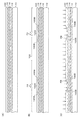
次に、図2及び図3を参照しながら、上述した実施例の製造方法を説明する。まず、図2(A)に示すように、基板10上に、下部電極12としてPtを200nm形成する。次に、誘電体層14として、BST(Ba1-xSrxTiO3)を200nm形成し、その上に、上部電極16としてPtを200nm形成する。これらにより、MIM構造のコンデンサないしキャパシタが得られる。このMIM構造の上には、スピンコート法によって、膜厚1μmのレジスト層100が形成される。レジスト層100としては、ポジ型フォトレジスト,例えば、ジアゾナフトキノン系ノボラック樹脂が使用される。レジスト材料を調整することで、テーパないし加工斜面100Bの角度を調整することができる。形成後、レジスト層100に対し、110℃/90secの条件でプリベークが行われる。
Next, the manufacturing method of the above-described embodiment will be described with reference to FIGS. First, as shown in FIG. 2A, 200 nm of Pt is formed as the
次に、図2(B)に示すように、所望のマスク102を用意し、g線を用いたプロキシミティ露光を行う(矢印FA参照)。このとき、所望のテーパ形状が得られるように、レジスト層100の露光部位100Aにおけるテーパ100Bの角度がコントロールされる。このコントロールは、例えば、プロキシミティ露光においてマスクとワークとの間の距離を変えることで実現される。露光後のレジスト層100に対しては、現像(露光部位100Aの除去),ベークの処理が順次行われ、図2(C)に示す状態となる。なお、ベーク温度を高温化(ガラス転位温度以上)すると、樹脂の相変化のため、同様に、テーパ100Bの角度を制御することができる。
Next, as shown in FIG. 2B, a desired
次に、図2(C)に矢印FBで示すように、例えばICP(高密度誘導結合プラズマ)を用いて、誘電体層14及び上部電極16のドライエッチングを行う。このとき残渣が発生するが、残渣のデポジション(堆積)の程度は、加工時に発生する残渣の堆積速度と、堆積した残渣の再除去速度の両者の競争反応となる。このため、デポジションする残渣の量は、加工斜面100Bに照射されるイオンエネルギー密度におおよそ比例するようになる。
Next, as indicated by an arrow FB in FIG. 2C, the
この加工斜面100Bに照射されるエネルギー密度は、テーパ角度α(図1参照)に対し、平面に照射されるイオンエネルギー密度をEHとすると、加工斜面100Bに入射するエネルギー密度ETとの間には、以下の関係が成り立つ。
ET∝EH・cosα
The energy density irradiated to the
ET∝EH ・ cosα
このため、照射イオンエネルギー密度EHは、テーパ角度αの高角度化により低下する結果となり、デポジションを除去する速度が低下する。従って、テーパ角度αが小さいほど、加工面に照射されるイオンエネルギー密度EHが増加し、加工残渣のデポジションレートに比べて付着した残渣の再除去速度が速くなる。また、ガス種などのエッチングパラメータを変えることによっても材料間の選択比を調整することができ、テーパ角度αを調整することができる。これらにより、高角度テーパで問題になっていたデポジション,トレンチ,異物などによるリークや歩留まりの悪化などの問題が改善されるようになる。 For this reason, the irradiation ion energy density EH is reduced as the taper angle α is increased, and the deposition removal speed is reduced. Therefore, the smaller the taper angle α, the higher the ion energy density EH applied to the processing surface, and the higher the removal rate of the attached residue as compared with the deposition rate of the processing residue. In addition, the selectivity between materials can be adjusted by changing etching parameters such as gas species, and the taper angle α can be adjusted. As a result, problems such as leakage due to deposition, trenches, foreign matter, etc. and deterioration of yield, which have been a problem with high-angle taper, are improved.
なお、デポジションの除去速度を速める方法として、プラズマイオンの入射エネルギーを強くする方法も考えられるが、こうした方法ではデポジションの生成速度も増加するだけではなく、マスクとなっているレジスト層100などへのダメージが発生することが確認されており、好ましくない。
As a method for increasing the deposition removal rate, a method of increasing the incident energy of plasma ions is also conceivable. However, in this method, not only the deposition generation rate is increased, but also the resist
表1には、以上のようにして得たサンプルにおけるデポジションの有無と不良率の割合(歩留まり)が示されている。
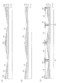
この表1に示すように、通常の加工条件の場合、加工後のテーパ角度は56°,加工残渣のデポジションがあり、全品が不良であった。次に、加工形状を低テーパ化し、テーパ角度αが42°付近では、依然として加工残渣デポジションがあり、不良率も81%であった。しかし、更に低テーパ化を図り、テーパ角度αを40°とすると、加工残渣デポジションはわずかとなるとともに不良率は68%まで低下し、テーパ角度αが30°になると、加工残渣デポジションはまったく見られず、不良率も36%まで低下した。テーパ角αを29°にすると不良率は33%になり、テーパ角度αが23°になると不良率は更に低下して5%となる。 As shown in Table 1, under normal processing conditions, the taper angle after processing was 56 °, there was deposition of processing residues, and all products were defective. Next, when the processing shape was reduced to a taper and the taper angle α was around 42 °, there was still processing residue deposition and the defect rate was 81%. However, if the taper angle α is 40 ° when the taper angle is further reduced, the processing residue deposition becomes small and the defect rate decreases to 68%. When the taper angle α is 30 °, the processing residue deposition is It was not seen at all, and the defect rate was reduced to 36%. When the taper angle α is 29 °, the defect rate is 33%, and when the taper angle α is 23 °, the defect rate is further reduced to 5%.
図3(A)には、以上のようにしてドライエッチングを行った後の様子が示されている。この後、同図(B)に示すように、酸素プラズマによって残存したレジスト100の除去(アッシング)を行う。更に、加工面に対して保護膜18,引出電極20,22を形成し、同図(C)のラインLAで切断することで、図1に示したMIM構造の薄膜コンデンサが得られる。図4(B)には、その一例が示されており、テーパ24に同図(A)に示した金属残渣のデポジション908はまったく観察されない。
FIG. 3A shows a state after dry etching is performed as described above. Thereafter, the remaining resist 100 is removed (ashed) by oxygen plasma, as shown in FIG. Further, the
以上のように、本実施例によれば、レジスト材料に形成するテーパの調整,露光条件の調整,レジスト材料のベーク温度の調整,エッチングレートの材料間の選択比の調整の少なくとも一つにより、誘電体層14と上部電極16に、中心部から端部に向かうテーパ24を形成することとしたので、加工時に発生する金属残渣の加工面へのデポジションの改善,加工端面に由来するリークの低減,歩留まり低下の改善,保護膜のカバレッジ向上,クラックやピンホールの低減という優れた効果が得られる。
As described above, according to this embodiment, at least one of adjustment of the taper formed in the resist material, adjustment of the exposure conditions, adjustment of the baking temperature of the resist material, and adjustment of the selection ratio between the etching rate materials, Since the
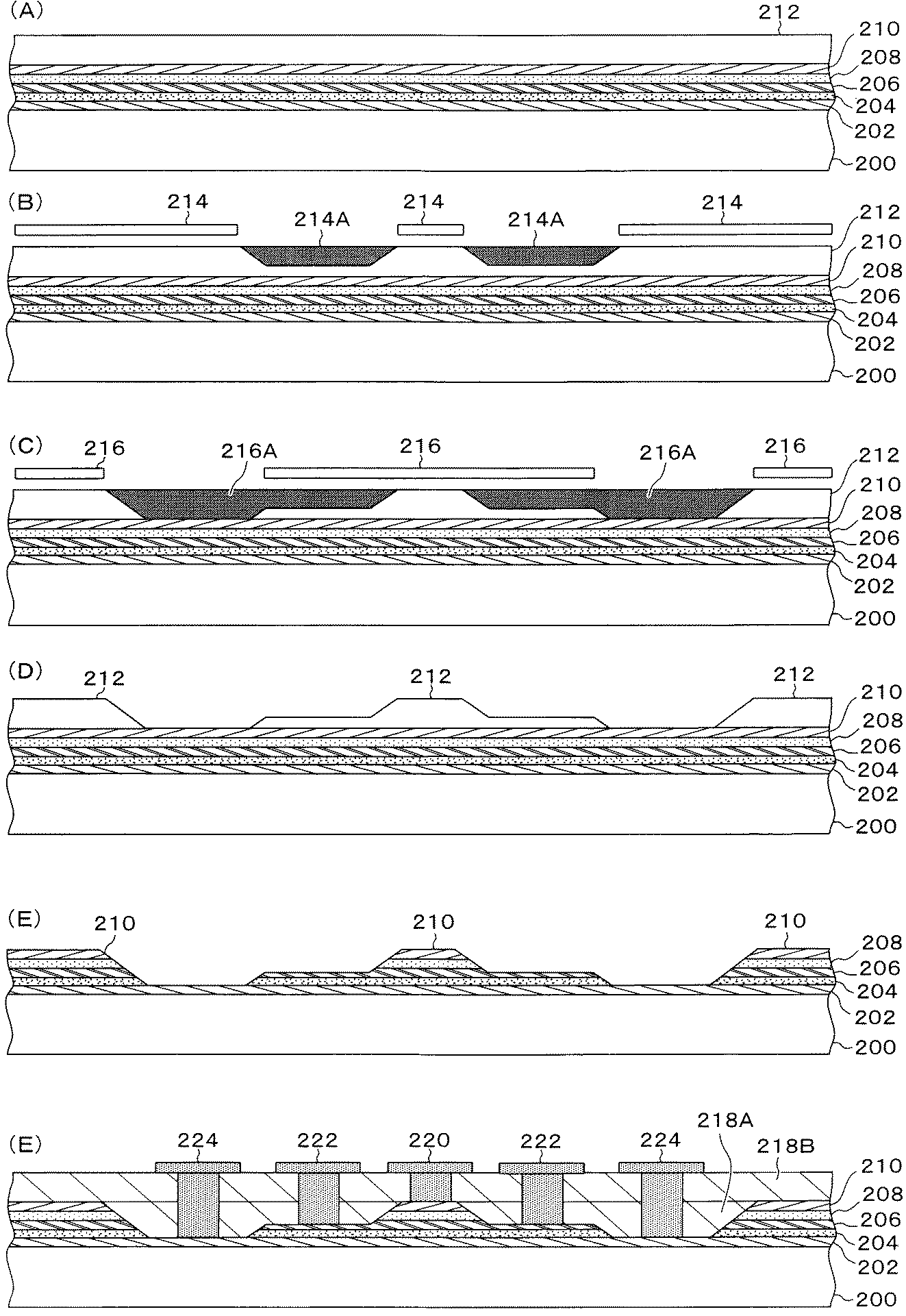
次に、図5を参照しながら、本発明の実施例2について説明する。上述した実施例1は、MIM構造を1層含む薄膜コンデンサの例であるが、この実施例2はMIM構造を2層含む例である。まず、図5(A)に示すように、基板200上に、下部電極202,第1誘電体層204,中間電極206,第2誘電体層208,上部電極210を順に積層形成する。下部電極202,中間電極206,上部電極210は例えばPtによって200nmの厚さに形成され、第1誘電体層204及び第2誘電体層208は例えばBSTによって200nmの厚さに形成される。これらの各層により、直列型のMIM構造のコンデンサないしキャパシタが得られる。このMIM構造の上には、スピンコート法によって、膜厚2μmのレジスト層212が形成される。レジスト層212としては、ポジ型フォトレジスト,例えば、ジアゾナフトキノン系ノボラック樹脂が使用される。レジスト材料を調整することで、テーパの角度を調整することができる。形成後、レジスト層212に対し、110℃/90secの条件でプリベークが行われる。
Next, Embodiment 2 of the present invention will be described with reference to FIG. The first embodiment described above is an example of a thin film capacitor including one layer of the MIM structure, but the second embodiment is an example including two layers of the MIM structure. First, as shown in FIG. 5A, a
続いて、レジスト層212の露光プロセスであるが、露光は、図5(B)及び(C)に示すように、2段階で実施する。1段階目は、マスク214を使用し、レジスト層212が0.8μm残存するようにプロキシミティ露光を実施する。これにより、図5(B)中の領域214Aが感光する。2段階目は、マスク214からマスク216に交換し、実施例1と同様にプロキシミティ露光を行う。これにより、図5(C)中の領域216Aが感光する。その後、レジスト層212の現像を行うと、同図(D)に示すようになる。
Subsequently, an exposure process for the resist
こうして得られた構造に対して、全層一括のエッチングを実施する。この結果、デポジションがなく、また、1層の場合と同様の信頼性を持つ多層膜のMIM構造を1回の加工によって作製することが可能となる。加工後の主面上には保護膜218A,218Bが形成され、各電極202,206,210上には引出電極224,222,220がそれぞれ形成される。なお、図5の例では、1種類のレジストを使用し、異なるマスクを使用して2回露光を行ったが、複数の種類のレジストを2層以上用いることによっても、同様の効果を得ることができる。
Etching of all layers is performed on the structure thus obtained. As a result, a multilayer MIM structure having no deposition and having the same reliability as in the case of a single layer can be manufactured by a single process.
本発明は、上述した実施例に限定されるものではなく、本発明の要旨を逸脱しない範囲内において種々変更を加え得ることができる。例えば、以下のものも含まれる。
(1)前記実施例に示した材料,形状,寸法は一例であり、同様の作用を奏するように適宜変更可能である。例えば、図1に示した薄膜コンデンサは平面が四角形であるが、これを円形としてもよい。
(2)前記実施例1では、誘電体層14及び上部電極16にテーパ24を形成したが、テーパ24が下部電極12に及ぶことを妨げるものではない。
The present invention is not limited to the above-described embodiments, and various modifications can be made without departing from the gist of the present invention. For example, the following are also included.
(1) The materials, shapes, and dimensions shown in the above embodiments are merely examples, and can be appropriately changed so as to achieve the same effect. For example, although the thin film capacitor shown in FIG. 1 has a square plane, it may be circular.
(2) In the first embodiment, the
本発明によれば、金属残渣の加工面へのデポジションが改善され、歩留まりや信頼性が向上するので、薄膜コンデンサの量産に好適である。 According to the present invention, the deposition of metal residue on the processed surface is improved, and the yield and reliability are improved, which is suitable for mass production of thin film capacitors.
10,200:基板
12,202:下部電極
14,204,208:誘電体層
16,210:上部電極
18,218A,218B:保護膜
20,22,220,222,224:引出電極
24:テーパ
26:中間電極
100,212:レジスト層
100A:露光部位
100B:テーパないし加工斜面
102,214,216:マスク
206:中間電極
214A,216A:領域
900:基板
902:下部電極
904:誘電体層
906:上部電極
908:デポジション
10, 200:
Claims (4)
少なくとも前記誘電体層及び上部電極の端部にテーパを形成するとともに、
前記テーパの角度を40°以下としたことを特徴とする薄膜コンデンサ。 A MIM type thin film capacitor in which a lower electrode, a dielectric layer, and an upper electrode are laminated,
Forming a taper at least at the ends of the dielectric layer and the upper electrode;
A thin film capacitor, wherein the taper angle is 40 ° or less.
ドライエッチングによって前記テーパを形成する際に、レジスト材料に形成するテーパの調整,露光条件の調整,レジスト材料のベーク温度の調整,エッチングレートの材料間の選択比の調整の少なくとも一つにより、前記テーパの角度を調整することを特徴とする薄膜コンデンサの製造方法。
It is a manufacturing method of the thin film capacitor in any one of Claims 1-3,
When forming the taper by dry etching, at least one of adjustment of the taper formed in the resist material, adjustment of exposure conditions, adjustment of the baking temperature of the resist material, adjustment of the selectivity of the etching rate between the materials, A method of manufacturing a thin film capacitor, wherein the taper angle is adjusted.
Priority Applications (1)
| Application Number | Priority Date | Filing Date | Title |
|---|---|---|---|
| JP2005317416A JP2007123768A (en) | 2005-10-31 | 2005-10-31 | Thin film capacitor and its manufacturing method |
Applications Claiming Priority (1)
| Application Number | Priority Date | Filing Date | Title |
|---|---|---|---|
| JP2005317416A JP2007123768A (en) | 2005-10-31 | 2005-10-31 | Thin film capacitor and its manufacturing method |
Publications (1)
| Publication Number | Publication Date |
|---|---|
| JP2007123768A true JP2007123768A (en) | 2007-05-17 |
Family
ID=38147244
Family Applications (1)
| Application Number | Title | Priority Date | Filing Date |
|---|---|---|---|
| JP2005317416A Withdrawn JP2007123768A (en) | 2005-10-31 | 2005-10-31 | Thin film capacitor and its manufacturing method |
Country Status (1)
| Country | Link |
|---|---|
| JP (1) | JP2007123768A (en) |
Cited By (3)
| Publication number | Priority date | Publication date | Assignee | Title |
|---|---|---|---|---|
| JP2018063978A (en) * | 2016-10-11 | 2018-04-19 | Tdk株式会社 | Thin film capacitor |
| KR20180056257A (en) * | 2016-11-18 | 2018-05-28 | 삼성전기주식회사 | Thin-film ceramic capacitor |
| JP2018200911A (en) * | 2017-05-25 | 2018-12-20 | 凸版印刷株式会社 | Glass circuit board and manufacturing method thereof |
-
2005
- 2005-10-31 JP JP2005317416A patent/JP2007123768A/en not_active Withdrawn
Cited By (4)
| Publication number | Priority date | Publication date | Assignee | Title |
|---|---|---|---|---|
| JP2018063978A (en) * | 2016-10-11 | 2018-04-19 | Tdk株式会社 | Thin film capacitor |
| KR20180056257A (en) * | 2016-11-18 | 2018-05-28 | 삼성전기주식회사 | Thin-film ceramic capacitor |
| KR102712634B1 (en) | 2016-11-18 | 2024-10-02 | 삼성전기주식회사 | Thin-film ceramic capacitor |
| JP2018200911A (en) * | 2017-05-25 | 2018-12-20 | 凸版印刷株式会社 | Glass circuit board and manufacturing method thereof |
Similar Documents
| Publication | Publication Date | Title |
|---|---|---|
| US11881432B2 (en) | Interconnect wires including relatively low resistivity cores | |
| TW201947648A (en) | Porous region structure and method of manufacture thereof | |
| TW394985B (en) | A semiconductor device having an improved contact structure and a manufacturing method thereof | |
| DE102011050934B4 (en) | Method for producing a semiconductor component | |
| JP2009295851A (en) | Semiconductor device, and method for manufacturing thereof | |
| TWI877158B (en) | Three-dimensional capacitive structures and their manufacturing methods | |
| US7659195B2 (en) | Method for forming metal line of semiconductor device | |
| JP2007123768A (en) | Thin film capacitor and its manufacturing method | |
| JP4395896B2 (en) | Manufacturing method of semiconductor device | |
| CN102243998A (en) | Method of manufacturing semiconductor device | |
| CN102522325B (en) | Production method for submicron multilayer metallic electrode | |
| TW200401463A (en) | Metal-insulator-metal (MIM) capacitor and method for fabricating the same | |
| JP4660119B2 (en) | Manufacturing method of semiconductor device | |
| CN115798944B (en) | Forming method of porous titanium electrode with high aspect ratio for micro supercapacitor | |
| US7566612B2 (en) | Method of fabricating capacitor in semiconductor device and semiconductor device using the same | |
| CN112119512B (en) | Porous region structure and method of manufacturing the same | |
| JPH1041481A (en) | High dielectric capacitor and semiconductor device | |
| Bossard | Tantalum Pentoxide Deposition and Applications | |
| CN118099094A (en) | Method for obtaining an integrated device comprising defining cut lines using an etching mask | |
| KR100791695B1 (en) | Hole photoresist pattern reforming method | |
| TW200828500A (en) | Method of manufacturing openings and via openings | |
| TWI509692B (en) | Semiconductor device and method of fabricating the same | |
| JP3499769B2 (en) | Method of forming oxide film, capacitor | |
| CN1450619A (en) | Method for making hybrid circuit element capacitor by ion implantation method | |
| KR101096232B1 (en) | Method for fabricating fuse in semiconductor device |
Legal Events
| Date | Code | Title | Description |
|---|---|---|---|
| A300 | Withdrawal of application because of no request for examination |
Free format text: JAPANESE INTERMEDIATE CODE: A300 Effective date: 20090106 |