JP2007123438A - Phosphor plate and light emitting device with same - Google Patents
Phosphor plate and light emitting device with same Download PDFInfo
- Publication number
- JP2007123438A JP2007123438A JP2005311624A JP2005311624A JP2007123438A JP 2007123438 A JP2007123438 A JP 2007123438A JP 2005311624 A JP2005311624 A JP 2005311624A JP 2005311624 A JP2005311624 A JP 2005311624A JP 2007123438 A JP2007123438 A JP 2007123438A
- Authority
- JP
- Japan
- Prior art keywords
- light
- phosphor plate
- phosphor
- light emitting
- led element
- Prior art date
- Legal status (The legal status is an assumption and is not a legal conclusion. Google has not performed a legal analysis and makes no representation as to the accuracy of the status listed.)
- Withdrawn
Links
Images


Classifications
-
- H—ELECTRICITY
- H01—ELECTRIC ELEMENTS
- H01L—SEMICONDUCTOR DEVICES NOT COVERED BY CLASS H10
- H01L33/00—Semiconductor devices with at least one potential-jump barrier or surface barrier specially adapted for light emission; Processes or apparatus specially adapted for the manufacture or treatment thereof or of parts thereof; Details thereof
- H01L33/48—Semiconductor devices with at least one potential-jump barrier or surface barrier specially adapted for light emission; Processes or apparatus specially adapted for the manufacture or treatment thereof or of parts thereof; Details thereof characterised by the semiconductor body packages
- H01L33/50—Wavelength conversion elements
- H01L33/501—Wavelength conversion elements characterised by the materials, e.g. binder
-
- H—ELECTRICITY
- H01—ELECTRIC ELEMENTS
- H01L—SEMICONDUCTOR DEVICES NOT COVERED BY CLASS H10
- H01L2224/00—Indexing scheme for arrangements for connecting or disconnecting semiconductor or solid-state bodies and methods related thereto as covered by H01L24/00
- H01L2224/01—Means for bonding being attached to, or being formed on, the surface to be connected, e.g. chip-to-package, die-attach, "first-level" interconnects; Manufacturing methods related thereto
- H01L2224/42—Wire connectors; Manufacturing methods related thereto
- H01L2224/47—Structure, shape, material or disposition of the wire connectors after the connecting process
- H01L2224/48—Structure, shape, material or disposition of the wire connectors after the connecting process of an individual wire connector
- H01L2224/4805—Shape
- H01L2224/4809—Loop shape
- H01L2224/48091—Arched
-
- H—ELECTRICITY
- H01—ELECTRIC ELEMENTS
- H01L—SEMICONDUCTOR DEVICES NOT COVERED BY CLASS H10
- H01L2224/00—Indexing scheme for arrangements for connecting or disconnecting semiconductor or solid-state bodies and methods related thereto as covered by H01L24/00
- H01L2224/01—Means for bonding being attached to, or being formed on, the surface to be connected, e.g. chip-to-package, die-attach, "first-level" interconnects; Manufacturing methods related thereto
- H01L2224/42—Wire connectors; Manufacturing methods related thereto
- H01L2224/47—Structure, shape, material or disposition of the wire connectors after the connecting process
- H01L2224/49—Structure, shape, material or disposition of the wire connectors after the connecting process of a plurality of wire connectors
- H01L2224/491—Disposition
- H01L2224/49105—Connecting at different heights
- H01L2224/49107—Connecting at different heights on the semiconductor or solid-state body
-
- H—ELECTRICITY
- H01—ELECTRIC ELEMENTS
- H01L—SEMICONDUCTOR DEVICES NOT COVERED BY CLASS H10
- H01L2933/00—Details relating to devices covered by the group H01L33/00 but not provided for in its subgroups
- H01L2933/0091—Scattering means in or on the semiconductor body or semiconductor body package
-
- H—ELECTRICITY
- H01—ELECTRIC ELEMENTS
- H01L—SEMICONDUCTOR DEVICES NOT COVERED BY CLASS H10
- H01L33/00—Semiconductor devices with at least one potential-jump barrier or surface barrier specially adapted for light emission; Processes or apparatus specially adapted for the manufacture or treatment thereof or of parts thereof; Details thereof
- H01L33/48—Semiconductor devices with at least one potential-jump barrier or surface barrier specially adapted for light emission; Processes or apparatus specially adapted for the manufacture or treatment thereof or of parts thereof; Details thereof characterised by the semiconductor body packages
- H01L33/483—Containers
- H01L33/486—Containers adapted for surface mounting
Abstract
Description
本発明は、発光素子から発せられる光を受けて励起されることにより波長変換光を発する蛍光体板及びこれを備えた発光装置に関する。 The present invention relates to a phosphor plate that emits wavelength-converted light when excited by receiving light emitted from a light-emitting element, and a light-emitting device including the phosphor plate.
周知のように、単一の発光ダイオード(Light Emitting Diode:LED)素子から発せられる光と、この光で励起されて発する波長変換光との混合により白色光を得ることができる発光装置が実用化されている。 As is well known, a light emitting device capable of obtaining white light by mixing light emitted from a single light emitting diode (LED) element and wavelength converted light emitted by being excited by this light is put into practical use. Has been.
従来、この種の発光装置には、光取出側に開口するケースを有するパッケージと、ケース内に収容されたLED素子と、LED素子をケース内で封止する蛍光体含有の封止部材とを備えたものが知られている(例えば特許文献1参照)。 Conventionally, this type of light emitting device includes a package having a case that opens to the light extraction side, an LED element housed in the case, and a phosphor-containing sealing member that seals the LED element in the case. What is provided is known (for example, refer patent document 1).
このような発光装置においては、LED素子として青色光を発する青色LED素子であり、また蛍光体として青色光で励起されて黄色光を発する蛍光体であると、LED素子から発せられる青色の励起光と蛍光体から発せられる黄色の波長変換光との混合により白色光が得られる。
しかし、特許文献1によると、次の(1)〜(3)に示す問題があった。
(1)LED素子からの光の一部が封止部材に吸収され、このため光吸収損失が生じ、光取出効率が低下する。
However, according to Patent Document 1, there are the following problems (1) to (3).
(1) A part of the light from the LED element is absorbed by the sealing member, so that a light absorption loss occurs, and the light extraction efficiency decreases.
(2)蛍光体含有の封止部材がLED素子に接触する構造であるため、LED素子の発光による発熱によって蛍光体が劣化する。この結果、蛍光体の波長変換効率が低下し、長期間にわたって高輝度の照射光を得ることができない。 (2) Since the phosphor-containing sealing member is in contact with the LED element, the phosphor deteriorates due to heat generated by light emission of the LED element. As a result, the wavelength conversion efficiency of the phosphor decreases, and high-intensity irradiation light cannot be obtained over a long period of time.
(3)蛍光体含有の封止部材がケース内に充填されているため、蛍光体の一部がケース底部に沈殿してその分布状態が悪くなるばかりか、LED素子から様々な方向に発せられる光の行路長が蛍光体含有の封止部材中で一定でなくなる。この結果、封止部材中で良好な波長変換が行われず、色むらが生じる。 (3) Since the phosphor-containing sealing member is filled in the case, a part of the phosphor is deposited on the bottom of the case and its distribution state is deteriorated, and the LED element is emitted in various directions. The path length of light is not constant in the phosphor-containing sealing member. As a result, favorable wavelength conversion is not performed in the sealing member, and color unevenness occurs.
従って、本発明の目的は、光取出効率を高めることができるとともに、長期間にわたって高輝度の照射光を得ることができ、かつ色むらを改善することができる蛍光体板及びこれを備えた発光装置を提供することにある。 Therefore, an object of the present invention is to increase the light extraction efficiency, obtain a high-intensity irradiation light over a long period of time, and improve the color unevenness, and a light emitting device including the phosphor plate To provide an apparatus.
(1)本発明は、上記目的を達成するために、発光素子の光取出側に配設され、前記発光素子から発せられる光を受けて励起されることにより波長変換光を発する蛍光体を基部材に含有してなる波長変換用の板部材であって、前記基部材には、前記光の進行方向を変換する光進行方向変換部が設けられていることを特徴とする蛍光体板を提供する。 (1) In order to achieve the above object, the present invention is based on a phosphor that is disposed on the light extraction side of a light emitting element and emits wavelength-converted light when excited by receiving light emitted from the light emitting element. Provided is a wavelength conversion plate member contained in a member, wherein the base member is provided with a light travel direction conversion section that converts the light travel direction. To do.
(2)本発明は、上記目的を達成するために、光取出側に開口する内部空間を有するケースと、前記ケースの光取出側に配設された蛍光体板と、前記蛍光体板の光反取出側に配設され、かつ前記ケース内に収容された発光素子とを備えた発光装置において、前記蛍光体板は、上記(1)に記載の蛍光体板であることを特徴とする発光装置を提供する。 (2) In order to achieve the above object, the present invention provides a case having an internal space that opens to the light extraction side, a phosphor plate disposed on the light extraction side of the case, and light from the phosphor plate. A light-emitting device provided with a light-emitting element disposed on the opposite side and housed in the case, wherein the phosphor plate is the phosphor plate described in (1) above. Providing equipment.
本発明によると、光取出効率を高めることができるとともに、長期間にわたって高輝度の照射光を得ることができ、かつ色むらを改善することができる。 According to the present invention, light extraction efficiency can be increased, irradiation light with high brightness can be obtained over a long period of time, and color unevenness can be improved.
[第1の実施の形態]
図1は、本発明の第1の実施の形態に係る蛍光体板を備えた発光装置を説明するために示す図である。図1(a)は発光装置全体の断面図を、図1(b)はLED素子の断面図をそれぞれ示す。
[First embodiment]
FIG. 1 is a view for explaining a light emitting device including a phosphor plate according to a first embodiment of the present invention. 1A is a cross-sectional view of the entire light emitting device, and FIG. 1B is a cross-sectional view of the LED element.
〔発光装置1の全体構成〕
図1(a)において、発光装置1は、素子収容用のパッケージ2と、このパッケージ2内に収容されたLED素子3と、パッケージ2内に充填されてLED素子3を封止する封止部材8と、LED素子3の光取出側に封止部材8を覆うように配置された蛍光体板4とから大略構成されている。
[Overall configuration of light-emitting device 1]
Referring to FIG. 1A, a light emitting device 1 includes an element housing package 2, an LED element 3 housed in the package 2, and a sealing member that fills the package 2 and seals the LED element 3. 8 and a phosphor plate 4 arranged so as to cover the sealing member 8 on the light extraction side of the LED element 3.
(パッケージ2の構成)
パッケージ2は、図1(a)に示すように、LED素子3を収容可能なケース5と、ケース5の一方側(図1では下側)開口部を覆う素子搭載基板6とを有している。
(Configuration of package 2)
As shown in FIG. 1A, the package 2 includes a case 5 that can accommodate the LED element 3 and an element mounting substrate 6 that covers an opening on one side (lower side in FIG. 1) of the case 5. Yes.
<ケース5の構成>
ケース5は、図1(a)に示すように、基板側から光取出側に向かって開口する平面円形状の内部空間5Aを有し、全体が例えばアルミナ(Al2O3)等のセラミックス材料からなる箱体によって形成されている。ケース5の材料としては、Al2O3の他にシリコン(Si)や窒化アルミニウム(AlN)あるいは白色樹脂が用いられる。ケース5内には、LED素子3からの光を光取出側に反射するための傾斜面5Bが設けられている。内部空間5Aの光取出側には、蛍光体板4を取り付けるための段状面5Cが設けられている。内部空間5Aには封止部材8が充填されている。
<Configuration of Case 5>
As shown in FIG. 1A, the case 5 has a planar circular internal space 5A that opens from the substrate side toward the light extraction side, and the entire case 5 is a ceramic material such as alumina (Al 2 O 3 ). It is formed by the box which consists of. As a material of the case 5, silicon (Si), aluminum nitride (AlN), or white resin is used in addition to Al 2 O 3 . In the case 5, an inclined surface 5B for reflecting the light from the LED element 3 to the light extraction side is provided. A stepped surface 5C for attaching the phosphor plate 4 is provided on the light extraction side of the internal space 5A. A sealing member 8 is filled in the internal space 5A.
<素子搭載基板6の構成>
素子搭載基板6はAl2O3のセラミックス材料によって形成されている。素子搭載基板6の材料としては、Al2O3の他に、SiやAlNあるいは白色樹脂が用いられる。素子搭載基板6の光取出側面(表面)には、LED素子3のp側電極3A及びn側電極3B(図1(b)に示す)にそれぞれ金(Au)からなるボンディングワイヤ12,13を介して接続する第1配線パターン14,15が設けられている。素子搭載基板6の実装側面(裏面)には、LED素子3に対して電源電圧を供給するための第2配線パターン16,17が設けられている。そして、第1配線パターン14と第2配線パターン16と及び第1配線パターン15と第2配線パターン17とは、それぞれ素子搭載基板6を貫通するビアホール19,20内に充填されたビアパターン22,23により電気的に接続されている。第1配線パターン14,15及び第2配線パターン16,17は、例えばタングステン(W),モリブデン(Mo)等の高融点金属によりビアパターン22,23と一体的に形成されている。
<Configuration of element mounting substrate 6>
The element mounting substrate 6 is made of an Al 2 O 3 ceramic material. As a material for the element mounting substrate 6, Si, AlN, or white resin is used in addition to Al 2 O 3 . On the light extraction side surface (surface) of the element mounting substrate 6, bonding wires 12 and 13 made of gold (Au) are respectively applied to the p-side electrode 3A and the n-side electrode 3B (shown in FIG. 1B) of the LED element 3. 1st wiring patterns 14 and 15 connected via are provided. Second wiring patterns 16 and 17 for supplying a power supply voltage to the LED element 3 are provided on the mounting side surface (back surface) of the element mounting substrate 6. The first wiring pattern 14 and the second wiring pattern 16, and the first wiring pattern 15 and the second wiring pattern 17 are respectively filled in via holes 19 and 20 penetrating the element mounting substrate 6, 23 is electrically connected. The first wiring patterns 14 and 15 and the second wiring patterns 16 and 17 are integrally formed with the via patterns 22 and 23 using a high melting point metal such as tungsten (W) or molybdenum (Mo).
なお、第1配線パターン14,15及び第2配線パターン16,17の表面には、ニッケル(Ni),アルミニウム(Al),白金(Pt),チタン(Ti),Au,銀(Ag),銅(Cu)など単層又は積層あるいは半田材料による金属層が必要に応じて形成される。 Note that nickel (Ni), aluminum (Al), platinum (Pt), titanium (Ti), Au, silver (Ag), copper are formed on the surfaces of the first wiring patterns 14 and 15 and the second wiring patterns 16 and 17. A single layer such as (Cu) or a laminated or metal layer made of a solder material is formed as necessary.
(封止部材8の構成)
封止部材8は、シリコーン等の光透過性樹脂材料からなり、素子搭載基板6と蛍光体板4との間に配置され、前述したようにケース5内でLED素子3を封止するように構成されている。封止部材8の材料としては、シリコーンの他に、エポキシ等の樹脂材料やN2,Ar等の不活性ガスが用いられる。
(Configuration of sealing member 8)
The sealing member 8 is made of a light-transmitting resin material such as silicone, and is disposed between the element mounting substrate 6 and the phosphor plate 4 so as to seal the LED element 3 in the case 5 as described above. It is configured. As a material of the sealing member 8, in addition to silicone, a resin material such as epoxy or an inert gas such as N 2 or Ar is used.
(LED素子3の構成)
LED素子3は、p側電極3A及びn側電極3B(共に図1(b)に示す)を有するフェイスアップ型の青色LED素子からなり、図1(a)に示すようにパッケージ2内の封止部材8によって封止され、かつ第1配線パターン14,15にボンディングワイヤ12,13を介して接続されている。LED素子3は、図1(b)に示すように、サファイア(Al2O3)基板24上にAlNからなるバッファ層(図示せず)及びn型半導体(n−GaN)層25・発光層26・p型半導体(p−GaN)層27を順次結晶成長させることにより形成されている。LED素子3の平面縦横寸法は、例えば縦寸法及び横寸法をそれぞれ約1mmとする平面サイズに設定されている。
(Configuration of LED element 3)
The LED element 3 is composed of a face-up blue LED element having a p-side electrode 3A and an n-side electrode 3B (both shown in FIG. 1B), and as shown in FIG. It is sealed by the stop member 8 and connected to the first wiring patterns 14 and 15 via bonding wires 12 and 13. As shown in FIG. 1B, the LED element 3 includes a buffer layer (not shown) made of AlN, an n-type semiconductor (n-GaN) layer 25, and a light emitting layer on a sapphire (Al 2 O 3 ) substrate 24. The 26.p-type semiconductor (p-GaN) layer 27 is formed by sequentially crystal growth. The planar vertical and horizontal dimensions of the LED element 3 are set to a planar size in which the vertical dimension and the horizontal dimension are about 1 mm, for example.
(蛍光体板4の構成)
蛍光体板4は、図1(a)に示すように、基部材4A及び蛍光体4Bからなり、ケース5の内部空間5Aに収容され、かつ段状面5Cに取り付けられている。蛍光体板4の厚さは均一な寸法(100μm〜500μm)に設定されている。
(Configuration of phosphor plate 4)
As shown in FIG. 1A, the phosphor plate 4 includes a base member 4A and a phosphor 4B, is accommodated in the internal space 5A of the case 5, and is attached to the stepped surface 5C. The thickness of the phosphor plate 4 is set to a uniform dimension (100 μm to 500 μm).
基部材4Aは、空気の屈折率n1(n1=1.0)より大きい屈性率n2(n2=1.4〜1.5)の光透過性(透明)材料からなる平面円形状の薄板によって形成されている。基部材4Aの材料としては、シリコーン,アクリル等の有機材料やガラス等の無機材料あるいは無機材料と有機材料との混合材料が用いられる。基部材4Aには、LED素子3からの光(青色光)の進行方向を変換する光進行方向変換部としての気泡9(屈折率n1)が含有されている。気泡9のサイズ(直径)は例えば100μm程度の寸法に、またその含有量割合は蛍光体板4の全体積に対して2〜3%の体積を占める割合にそれぞれ設定されている。 The base member 4A is a flat circular thin plate made of a light-transmitting (transparent) material having a refractive index n2 (n2 = 1.4 to 1.5) greater than the refractive index n1 (n1 = 1.0) of air. Is formed. As the material of the base member 4A, an organic material such as silicone or acrylic, an inorganic material such as glass, or a mixed material of an inorganic material and an organic material is used. The base member 4 </ b> A contains bubbles 9 (refractive index n <b> 1) as a light traveling direction conversion unit that converts the traveling direction of light (blue light) from the LED element 3. The size (diameter) of the bubbles 9 is set to, for example, a dimension of about 100 μm, and the content ratio is set to a ratio that occupies a volume of 2 to 3% with respect to the entire volume of the phosphor plate 4.
蛍光体4Bは基部材4Aに含有されている。そして、LED素子3からの青色光を受けて励起されることにより、波長変換光(黄色光)を発するYAG(YttriumAluminum Garnet)等の材料によって形成されている。 The phosphor 4B is contained in the base member 4A. And it is formed with materials, such as YAG (YttriumAluminum Garnet) which emits wavelength conversion light (yellow light) by receiving and exciting the blue light from LED element 3. FIG.
〔発光装置1の動作〕
先ず、LED素子3に電源から第2配線パターン16,17及びビアパターン22,23・第1配線パターン14,15・ボンディングワイヤ12,13を介して電圧が印加されると、LED素子3の発光層26において青色光を発し、この青色光がLED素子3の光取出面から封止部材8に出射される。
[Operation of Light Emitting Device 1]
First, when a voltage is applied to the LED element 3 from the power source via the second wiring patterns 16 and 17 and the via patterns 22 and 23, the first wiring patterns 14 and 15, and the bonding wires 12 and 13, the LED element 3 emits light. Blue light is emitted from the layer 26, and this blue light is emitted from the light extraction surface of the LED element 3 to the sealing member 8.
次に、LED素子3からの出射光が封止部材8を透過して蛍光体板4に入射する。この場合、LED素子3からの出射光の一部が封止部材8を透過し、またケース5の傾斜面5Bで反射してから封止部材8を透過し、それぞれ蛍光体板4に入射する。 Next, the emitted light from the LED element 3 passes through the sealing member 8 and enters the phosphor plate 4. In this case, a part of the light emitted from the LED element 3 is transmitted through the sealing member 8, reflected by the inclined surface 5 </ b> B of the case 5, then transmitted through the sealing member 8, and incident on the phosphor plate 4. .
そして、蛍光体板4(蛍光体4B)では入射した青色光を受けて励起されることにより黄色の波長変換光を発する。このため、LED素子3から発せられる青色光と蛍光体4Bから発せられる黄色光とが混合して白色光となる。この場合、蛍光体板4に入射した青色光の一部は、蛍光体板4中の気泡9に入射する。この際、気泡9の界面で進行方向を変換して反射され、青色光は蛍光体4Bに入射する。また、気泡9に入射する青色光はその内部で屈折し、さらに気泡9から出射する際に屈折して蛍光体4Bに入射する。これにより、青色光の一部が基部材4Aに吸収されず、光吸収損失の発生を抑制した状態で白色光が生成される。この後、白色光が蛍光体板4を透過し、蛍光体板4の光出射面から外部に出射される。 The phosphor plate 4 (phosphor 4B) emits yellow wavelength-converted light when excited by receiving the incident blue light. For this reason, the blue light emitted from the LED element 3 and the yellow light emitted from the phosphor 4B are mixed to become white light. In this case, part of the blue light incident on the phosphor plate 4 enters the bubbles 9 in the phosphor plate 4. At this time, the traveling direction is changed and reflected at the interface of the bubbles 9, and the blue light enters the phosphor 4B. Further, the blue light incident on the bubble 9 is refracted inside, and further refracted when entering from the bubble 9 and enters the phosphor 4B. Thereby, a part of blue light is not absorbed by the base member 4A, and white light is generated in a state where generation of light absorption loss is suppressed. Thereafter, white light passes through the phosphor plate 4 and is emitted to the outside from the light emitting surface of the phosphor plate 4.
[第1の実施の形態の効果]
以上説明した第1の実施の形態によれば、次に示す効果が得られる。
[Effect of the first embodiment]
According to the first embodiment described above, the following effects can be obtained.
(1)LED素子3からの青色光の一部が封止部材8に吸収されず、このため光吸収損失の発生を抑制することができ、光取出効率を高めること(20〜30%向上)ができる。 (1) Part of the blue light from the LED element 3 is not absorbed by the sealing member 8, so that the occurrence of light absorption loss can be suppressed, and the light extraction efficiency is increased (20-30% improvement). Can do.
(2)LED素子3の発熱による蛍光体4Bの劣化発生を抑制することができるため、蛍光体4Bの波長変換効率を高めることでき、長期間にわたって高輝度の照射光を得ることができる。 (2) Since the deterioration of the phosphor 4B due to the heat generated by the LED element 3 can be suppressed, the wavelength conversion efficiency of the phosphor 4B can be increased, and irradiation light with high brightness can be obtained over a long period of time.
(3)蛍光体板4(基部材4A)中で蛍光体4Bの分布状態が良好であるとともに、LED素子3から様々な方向に発せられる光の行路長が蛍光体板4中で一定であり、このため蛍光体板4中で良好な波長変換が行われ、色むらを改善することができる。 (3) The phosphor 4B is well distributed in the phosphor plate 4 (base member 4A), and the path length of light emitted from the LED elements 3 in various directions is constant in the phosphor plate 4. For this reason, favorable wavelength conversion is performed in the phosphor plate 4, and color unevenness can be improved.
[第2の実施の形態]
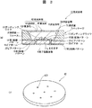
図2は、本発明の第2の実施の形態に係る蛍光体板を備えた発光装置を説明するために示す断面図である。図2において、図1と同一の部材については同一の符号を付し、詳細な説明は省略する。
[Second Embodiment]
FIG. 2 is a cross-sectional view for explaining a light emitting device including a phosphor plate according to a second embodiment of the present invention. 2, the same members as those in FIG. 1 are denoted by the same reference numerals, and detailed description thereof is omitted.
図2に示すように、第2の実施の形態に示す発光装置31は、光進行方向変換部として粒子を用いた点に特徴がある。 As shown in FIG. 2, the light emitting device 31 shown in the second embodiment is characterized in that particles are used as the light traveling direction conversion unit.
このため、基部材4Aには、LED素子3からの青色光の進行方向を変換する粒子として例えばシリカ(SiO2)からなるビーズ32(屈折率n3=1.4)が含有されている。ビーズ32のサイズ(直径)は例えば20μm〜100μm程度の寸法に、またその含有量割合は蛍光体板4の全体積に対して2〜3%の体積を占める割合にそれぞれ設定されている。 For this reason, the base member 4A contains beads 32 (refractive index n3 = 1.4) made of, for example, silica (SiO 2 ) as particles for converting the traveling direction of the blue light from the LED element 3. The size (diameter) of the beads 32 is set to a size of about 20 μm to 100 μm, for example, and the content ratio thereof is set to a ratio occupying a volume of 2 to 3% with respect to the total volume of the phosphor plate 4.
[第2の実施の形態の効果]
以上説明した第2の実施の形態によれば、第1の実施の形態の効果(1)〜(3)と同様の効果が得られる。
[Effect of the second embodiment]
According to the second embodiment described above, the same effects as the effects (1) to (3) of the first embodiment can be obtained.
[第3の実施の形態]
図3は、本発明の第3の実施の形態に係る蛍光体板を備えた発光装置を説明するために示す図である。図3(a)は発光装置全体の断面図を、また図3(b)は蛍光体板の斜視図を示す。図3(a)及び(b)において、図1と同一の部材については同一の符号を付し、詳細な説明は省略する。
[Third embodiment]
FIG. 3 is a diagram for explaining a light emitting device including a phosphor plate according to a third embodiment of the present invention. 3A is a sectional view of the entire light emitting device, and FIG. 3B is a perspective view of the phosphor plate. 3A and 3B, the same members as those in FIG. 1 are denoted by the same reference numerals, and detailed description thereof is omitted.
図3(a)に示すように、第3の実施の形態に示す発光装置41は、貫通孔42Aを有する蛍光体板42を備えた点に特徴がある。
As shown in FIG. 3A, the light emitting device 41 shown in the third embodiment is characterized in that it includes a
このため、蛍光体板42の貫通孔42Aは、蛍光体板42の光入射面及び光出射面に開口する丸孔によって形成され、その内部の空気層が光進行方向変換部として機能するように構成されている。これにより、蛍光体板42中に入射したLED素子3からの青色光の一部が貫通孔42A内の空気層と基部材4Aとの界面で進行方向を変換して反射され、蛍光体4Bに入射する。また、貫通孔42A内の空気層に入射する青色光の一部はその内部で屈折し、さらに貫通孔42A内から外部に出射する際に蛍光体4Bに入射する。
For this reason, the through-
[第3の実施の形態の効果]
以上説明した第3の実施の形態によれば、第1の実施の形態の効果(1)〜(3)と同様の効果が得られる。
[Effect of the third embodiment]
According to the third embodiment described above, the same effects as the effects (1) to (3) of the first embodiment can be obtained.
なお、本実施の形態においては、貫通孔42A内が空気層である場合について説明したが、本発明はこれに限定されず、基部材4Aの屈折率より小さい屈折率をもつガラス等の充填物であってもよい。
In the present embodiment, the case where the inside of the through
以上、本発明の発光装置を上記の実施の形態に基づいて説明したが、本発明は上記の実施の形態に限定されるものではなく、その要旨を逸脱しない範囲で種々の態様において実施することが可能であり、例えば次に示すような変形も可能である。 As mentioned above, although the light-emitting device of this invention was demonstrated based on said embodiment, this invention is not limited to said embodiment, It implements in a various aspect in the range which does not deviate from the summary. For example, the following modifications are possible.
(1)本実施の形態では、LED素子3から発せられる青色光を受けて励起されることにより黄色の波長変換光を発する蛍光体板4,42である場合について説明したが、本発明はこれに限定されず、LED素子から発せられる紫色光(波長370〜390nm)を受けて励起されることにより白色の波長変換光を発する蛍光体板であってもよい。
(1) In the present embodiment, the case where the
(2)本実施の形態では、フェイスアップ型のLED素子3を用いたが、フェイスダウン型のLED素子3を用いてもよい。この場合、LED素子3は第1配線パターン14,15にフリップ実装される。 (2) Although the face-up type LED element 3 is used in the present embodiment, the face-down type LED element 3 may be used. In this case, the LED element 3 is flip-mounted on the first wiring patterns 14 and 15.
1,31,41…発光装置、2…パッケージ、3…LED素子、3A…p側電極、3B…n側電極、4,42…蛍光体板、4A…基部材、4B…蛍光体、5…ケース、5A…内部空間、5B…傾斜面、5C…段状面、6…素子搭載基板、8…封止部材、9…気泡、12,13…ボンディングワイヤ、14,15…第1配線パターン、16,17…第2配線パターン、19,20…ビアホール、22,23…ビアパターン、24…サファイア基板、25…n型半導体層、26…発光層、27…p型半導体層、32…ビーズ、42A…貫通孔 DESCRIPTION OF SYMBOLS 1,31,41 ... Light-emitting device, 2 ... Package, 3 ... LED element, 3A ... P side electrode, 3B ... N side electrode, 4, 42 ... Phosphor plate, 4A ... Base member, 4B ... Phosphor, 5 ... Case, 5A: Internal space, 5B: Inclined surface, 5C ... Stepped surface, 6 ... Element mounting substrate, 8 ... Sealing member, 9 ... Bubble, 12, 13 ... Bonding wire, 14, 15 ... First wiring pattern, 16, 17 ... second wiring pattern, 19, 20 ... via hole, 22, 23 ... via pattern, 24 ... sapphire substrate, 25 ... n-type semiconductor layer, 26 ... light emitting layer, 27 ... p-type semiconductor layer, 32 ... bead, 42A ... through hole
Claims (7)
前記基部材には、前記光の進行方向を変換する光進行方向変換部が設けられていることを特徴とする蛍光体板。 A plate member for wavelength conversion, which is disposed on a light extraction side of a light emitting element and contains a phosphor that emits wavelength converted light by receiving and emitting light emitted from the light emitting element. ,
The phosphor plate according to claim 1, wherein the base member is provided with a light traveling direction conversion unit that converts the traveling direction of the light.
前記ケースの光取出側に配設された蛍光体板と、
前記蛍光体板の光反取出側に配設され、かつ前記ケース内に収容された発光素子とを備えた発光装置において、
前記蛍光体板は、請求項1乃至6のいずれかに記載の蛍光体板であることを特徴とする発光装置。 A case having an internal space opening on the light extraction side;
A phosphor plate disposed on the light extraction side of the case;
In a light emitting device provided with a light emitting element disposed on the light extraction side of the phosphor plate and housed in the case,
The phosphor plate is the phosphor plate according to claim 1, wherein the phosphor plate is a light emitting device.
Priority Applications (3)
| Application Number | Priority Date | Filing Date | Title |
|---|---|---|---|
| JP2005311624A JP2007123438A (en) | 2005-10-26 | 2005-10-26 | Phosphor plate and light emitting device with same |
| US11/581,751 US20070120463A1 (en) | 2005-10-26 | 2006-10-17 | Phosphor plate and light emitting device having same |
| CN200610150797.9A CN1956232A (en) | 2005-10-26 | 2006-10-26 | Phosphor plate and light emitting device having same |
Applications Claiming Priority (1)
| Application Number | Priority Date | Filing Date | Title |
|---|---|---|---|
| JP2005311624A JP2007123438A (en) | 2005-10-26 | 2005-10-26 | Phosphor plate and light emitting device with same |
Publications (2)
| Publication Number | Publication Date |
|---|---|
| JP2007123438A true JP2007123438A (en) | 2007-05-17 |
| JP2007123438A5 JP2007123438A5 (en) | 2008-01-17 |
Family
ID=38063420
Family Applications (1)
| Application Number | Title | Priority Date | Filing Date |
|---|---|---|---|
| JP2005311624A Withdrawn JP2007123438A (en) | 2005-10-26 | 2005-10-26 | Phosphor plate and light emitting device with same |
Country Status (3)
| Country | Link |
|---|---|
| US (1) | US20070120463A1 (en) |
| JP (1) | JP2007123438A (en) |
| CN (1) | CN1956232A (en) |
Cited By (4)
| Publication number | Priority date | Publication date | Assignee | Title |
|---|---|---|---|---|
| JP2008306013A (en) * | 2007-06-08 | 2008-12-18 | Ushio Inc | Illumination device |
| KR100882204B1 (en) | 2007-08-08 | 2009-02-06 | (주) 아모엘이디 | Semiconductor package |
| JP2010035922A (en) * | 2008-08-07 | 2010-02-18 | Olympus Corp | Light source unit and endoscope system using the same |
| JP2014116459A (en) * | 2012-12-10 | 2014-06-26 | Stanley Electric Co Ltd | Semiconductor light-emitting device |
Families Citing this family (44)
| Publication number | Priority date | Publication date | Assignee | Title |
|---|---|---|---|---|
| JP5073946B2 (en) * | 2005-12-27 | 2012-11-14 | 新光電気工業株式会社 | Semiconductor device and manufacturing method of semiconductor device |
| US7942556B2 (en) * | 2007-06-18 | 2011-05-17 | Xicato, Inc. | Solid state illumination device |
| KR100880638B1 (en) * | 2007-07-06 | 2009-01-30 | 엘지전자 주식회사 | Light emitting device package |
| US8118447B2 (en) | 2007-12-20 | 2012-02-21 | Altair Engineering, Inc. | LED lighting apparatus with swivel connection |
| CN100483762C (en) * | 2008-02-25 | 2009-04-29 | 鹤山丽得电子实业有限公司 | LED device making method |
| JP2011515536A (en) * | 2008-03-21 | 2011-05-19 | ナノグラム・コーポレイション | Metallic silicon nitride or metallic silicon oxynitride submicron phosphor particles and method of synthesizing these particles |
| US8901823B2 (en) | 2008-10-24 | 2014-12-02 | Ilumisys, Inc. | Light and light sensor |
| US8214084B2 (en) | 2008-10-24 | 2012-07-03 | Ilumisys, Inc. | Integration of LED lighting with building controls |
| US8653984B2 (en) | 2008-10-24 | 2014-02-18 | Ilumisys, Inc. | Integration of LED lighting control with emergency notification systems |
| US8324817B2 (en) | 2008-10-24 | 2012-12-04 | Ilumisys, Inc. | Light and light sensor |
| US7938562B2 (en) | 2008-10-24 | 2011-05-10 | Altair Engineering, Inc. | Lighting including integral communication apparatus |
| US7928655B2 (en) * | 2008-11-10 | 2011-04-19 | Visera Technologies Company Limited | Light-emitting diode device and method for fabricating the same |
| US20100127289A1 (en) * | 2008-11-26 | 2010-05-27 | Bridgelux, Inc. | Method and Apparatus for Providing LED Package with Controlled Color Temperature |
| JP5327601B2 (en) | 2008-12-12 | 2013-10-30 | 東芝ライテック株式会社 | Light emitting module and lighting device |
| US20100186066A1 (en) * | 2009-01-20 | 2010-07-22 | Pollard Stephen M | Methods and systems for facilitating personal data propagation |
| US8296323B2 (en) * | 2009-01-20 | 2012-10-23 | Titanium Fire Ltd. | Personal data subscriber systems and methods |
| EP2446190A4 (en) * | 2009-06-23 | 2013-02-20 | Ilumisys Inc | Led lamp with a wavelength converting layer |
| JP2011040494A (en) * | 2009-08-07 | 2011-02-24 | Koito Mfg Co Ltd | Light emitting module |
| US8258524B2 (en) * | 2010-01-26 | 2012-09-04 | Sharp Kabushiki Kaisha | Light emitting diode device |
| WO2011119921A2 (en) | 2010-03-26 | 2011-09-29 | Altair Engineering, Inc. | Led light with thermoelectric generator |
| US8540401B2 (en) | 2010-03-26 | 2013-09-24 | Ilumisys, Inc. | LED bulb with internal heat dissipating structures |
| DE102010034913B4 (en) | 2010-08-20 | 2023-03-30 | OSRAM Opto Semiconductors Gesellschaft mit beschränkter Haftung | Radiation-emitting component and method for producing the radiation-emitting component |
| TWI449866B (en) * | 2010-09-30 | 2014-08-21 | Hon Hai Prec Ind Co Ltd | Led illuminating device |
| US8523394B2 (en) | 2010-10-29 | 2013-09-03 | Ilumisys, Inc. | Mechanisms for reducing risk of shock during installation of light tube |
| US8901578B2 (en) | 2011-05-10 | 2014-12-02 | Rohm Co., Ltd. | LED module having LED chips as light source |
| US9184518B2 (en) | 2012-03-02 | 2015-11-10 | Ilumisys, Inc. | Electrical connector header for an LED-based light |
| TWM443813U (en) * | 2012-03-06 | 2012-12-21 | Winsky Technology Ltd | Illumination device |
| US9163794B2 (en) | 2012-07-06 | 2015-10-20 | Ilumisys, Inc. | Power supply assembly for LED-based light tube |
| US9271367B2 (en) | 2012-07-09 | 2016-02-23 | Ilumisys, Inc. | System and method for controlling operation of an LED-based light |
| US10125971B2 (en) * | 2013-02-19 | 2018-11-13 | Michael Graziano | LED lamp integrated to electric fan |
| US9285084B2 (en) | 2013-03-14 | 2016-03-15 | Ilumisys, Inc. | Diffusers for LED-based lights |
| US9267650B2 (en) | 2013-10-09 | 2016-02-23 | Ilumisys, Inc. | Lens for an LED-based light |
| CA2937642A1 (en) | 2014-01-22 | 2015-07-30 | Ilumisys, Inc. | Led-based light with addressed leds |
| US9510400B2 (en) | 2014-05-13 | 2016-11-29 | Ilumisys, Inc. | User input systems for an LED-based light |
| US10249599B2 (en) | 2016-06-29 | 2019-04-02 | eLux, Inc. | Laminated printed color conversion phosphor sheets |
| US9985190B2 (en) | 2016-05-18 | 2018-05-29 | eLux Inc. | Formation and structure of post enhanced diodes for orientation control |
| US9755110B1 (en) | 2016-07-27 | 2017-09-05 | Sharp Laboratories Of America, Inc. | Substrate with topological features for steering fluidic assembly LED disks |
| US9892944B2 (en) | 2016-06-23 | 2018-02-13 | Sharp Kabushiki Kaisha | Diodes offering asymmetric stability during fluidic assembly |
| US9917226B1 (en) | 2016-09-15 | 2018-03-13 | Sharp Kabushiki Kaisha | Substrate features for enhanced fluidic assembly of electronic devices |
| US10161568B2 (en) | 2015-06-01 | 2018-12-25 | Ilumisys, Inc. | LED-based light with canted outer walls |
| DE102016106841B3 (en) * | 2015-12-18 | 2017-03-23 | Fraunhofer-Gesellschaft zur Förderung der angewandten Forschung e.V. | Converter for generating a secondary light from a primary light, bulbs containing such converters, and methods for producing the converter and lighting means |
| US9627437B1 (en) | 2016-06-30 | 2017-04-18 | Sharp Laboratories Of America, Inc. | Patterned phosphors in through hole via (THV) glass |
| US10243097B2 (en) | 2016-09-09 | 2019-03-26 | eLux Inc. | Fluidic assembly using tunable suspension flow |
| US9837390B1 (en) | 2016-11-07 | 2017-12-05 | Corning Incorporated | Systems and methods for creating fluidic assembly structures on a substrate |
Family Cites Families (2)
| Publication number | Priority date | Publication date | Assignee | Title |
|---|---|---|---|---|
| US6635363B1 (en) * | 2000-08-21 | 2003-10-21 | General Electric Company | Phosphor coating with self-adjusting distance from LED chip |
| US20020084745A1 (en) * | 2000-12-29 | 2002-07-04 | Airma Optoelectronics Corporation | Light emitting diode with light conversion by dielectric phosphor powder |
-
2005
- 2005-10-26 JP JP2005311624A patent/JP2007123438A/en not_active Withdrawn
-
2006
- 2006-10-17 US US11/581,751 patent/US20070120463A1/en not_active Abandoned
- 2006-10-26 CN CN200610150797.9A patent/CN1956232A/en active Pending
Cited By (4)
| Publication number | Priority date | Publication date | Assignee | Title |
|---|---|---|---|---|
| JP2008306013A (en) * | 2007-06-08 | 2008-12-18 | Ushio Inc | Illumination device |
| KR100882204B1 (en) | 2007-08-08 | 2009-02-06 | (주) 아모엘이디 | Semiconductor package |
| JP2010035922A (en) * | 2008-08-07 | 2010-02-18 | Olympus Corp | Light source unit and endoscope system using the same |
| JP2014116459A (en) * | 2012-12-10 | 2014-06-26 | Stanley Electric Co Ltd | Semiconductor light-emitting device |
Also Published As
| Publication number | Publication date |
|---|---|
| US20070120463A1 (en) | 2007-05-31 |
| CN1956232A (en) | 2007-05-02 |
Similar Documents
| Publication | Publication Date | Title |
|---|---|---|
| JP2007123438A (en) | Phosphor plate and light emitting device with same | |
| US7855501B2 (en) | LED with phosphor layer having different thickness or different phosphor concentration | |
| JP5557828B2 (en) | Light emitting device | |
| US7910940B2 (en) | Semiconductor light-emitting device | |
| JP5919504B2 (en) | Light emitting device | |
| JP5326837B2 (en) | Light emitting device | |
| JP2007109946A (en) | Phosphor plate and light-emitting device provided with the same | |
| JP2007109947A (en) | Phosphor plate and light-emitting device provided with the same | |
| JP2007134656A (en) | Fluorescent board and light emitting device having it | |
| JP2007335798A (en) | Light-emitting device | |
| JP2005093712A (en) | Semiconductor light emitting device | |
| JP2010034184A (en) | Light-emitting device | |
| JP2002033520A (en) | Semiconductor light emitting device | |
| JP2007123437A (en) | Phosphor plate and light emitting device with same | |
| JP2007035802A (en) | Light-emitting device | |
| JP2008071954A (en) | Light source device | |
| JP2015176960A (en) | light-emitting device | |
| JP2005167079A (en) | Light emitting device | |
| JP2010034183A (en) | Light-emitting device | |
| JP2007201301A (en) | Light emitting device using white led | |
| JP2007109948A (en) | Light-emitting device and manufacturing method thereof | |
| JP2009267039A (en) | Light-emitting device | |
| JP2007066939A (en) | Semiconductor light emitting device | |
| JP2007042687A (en) | Light emitting diode device | |
| JP2012009633A (en) | Light-emitting device |
Legal Events
| Date | Code | Title | Description |
|---|---|---|---|
| A521 | Written amendment |
Free format text: JAPANESE INTERMEDIATE CODE: A523 Effective date: 20071127 |
|
| A621 | Written request for application examination |
Free format text: JAPANESE INTERMEDIATE CODE: A621 Effective date: 20071128 |
|
| A761 | Written withdrawal of application |
Free format text: JAPANESE INTERMEDIATE CODE: A761 Effective date: 20090525 |