JP2007072276A - Electrophotographic apparatus - Google Patents
Electrophotographic apparatus Download PDFInfo
- Publication number
- JP2007072276A JP2007072276A JP2005260653A JP2005260653A JP2007072276A JP 2007072276 A JP2007072276 A JP 2007072276A JP 2005260653 A JP2005260653 A JP 2005260653A JP 2005260653 A JP2005260653 A JP 2005260653A JP 2007072276 A JP2007072276 A JP 2007072276A
- Authority
- JP
- Japan
- Prior art keywords
- electrophotographic
- photosensitive member
- layer
- electrophotographic photosensitive
- resin
- Prior art date
- Legal status (The legal status is an assumption and is not a legal conclusion. Google has not performed a legal analysis and makes no representation as to the accuracy of the status listed.)
- Pending
Links
Images

Abstract
Description
本発明は、クリーナーレス方式の電子写真装置に関する。 The present invention relates to a cleanerless electrophotographic apparatus.
従来、複写機、プリンター、ファクシミリ等の電子写真方式を用いた電子写真装置は、潜像担持体である電子写真感光体、この感光体を帯電処理する帯電手段、感光体上に形成された静電潜像を現像剤であるトナーにより顕像化する現像手段、紙などの転写材に顕像化されたトナーを転写する転写手段、その後の感光体上に残された残留トナーをクリーニングするクリーニング手段、転写材上のトナーを定着させる定着手段などから構成される。 2. Description of the Related Art Conventionally, an electrophotographic apparatus using an electrophotographic system such as a copying machine, a printer, or a facsimile is an electrophotographic photosensitive member that is a latent image carrier, a charging unit that charges the photosensitive member, and a static image formed on the photosensitive member. Developing means for visualizing the electrostatic latent image with toner as developer, transfer means for transferring the visualized toner onto a transfer material such as paper, and cleaning for cleaning residual toner remaining on the photoreceptor thereafter And fixing means for fixing the toner on the transfer material.
電子写真感光体としては、使用する染料や顔料等の選択により感光波長域を自在にコントロールすることができ、成膜性が良く、生産性が高く、安価である等の利点を有することから、有機光導電性材料を用いた電子写真感光体が広く使用されている。この有機電子写真感光体は、導電性基体上に電荷発生材料や電荷輸送材料を溶解又は分散させた薄い樹脂層から構成されるため、無機感光体と比べて機械的耐久性が劣るという問題を有する。耐久性を改善させるために様々な開発が行われているが、近年、電子写真感光体上に硬度の高い表面層を設けることにより、感光体の削れ量を低減させ、長寿命化を図る提案がなされている(例えば、特許文献1及び2参照)。
As an electrophotographic photoreceptor, the photosensitive wavelength range can be freely controlled by selecting the dye or pigment to be used, and it has advantages such as good film forming properties, high productivity, and low cost. Electrophotographic photoreceptors using organic photoconductive materials are widely used. Since this organic electrophotographic photoreceptor is composed of a thin resin layer in which a charge generating material or a charge transporting material is dissolved or dispersed on a conductive substrate, the mechanical durability is inferior to that of an inorganic photoreceptor. Have. Various developments have been made to improve durability, but in recent years a proposal has been made to reduce the amount of photoconductor abrasion and extend the life by providing a hard surface layer on the electrophotographic photoreceptor. (For example, see
一方、電子写真装置全体の小型化、廃トナーレス化によるエコロジー対応や感光体磨耗量低減のために、クリーニング手段にて回収されている転写残トナーいわゆる廃トナーを現像手段に戻し再利用するクリーナーレス電子写真装置が開発されている。この一つの方式として、現像手段が転写後の残トナーを回収する方式を採用した複写機やプリンターが提案されている(例えば、特許文献3参照)。 On the other hand, in order to reduce the size of the entire electrophotographic apparatus, reduce the amount of waste toner, and reduce the amount of photoconductor wear, a cleaner that recycles the residual transfer toner recovered by the cleaning means to the developing means for reuse. Less electrophotographic devices have been developed. As one of the methods, a copying machine or a printer that employs a method in which a developing unit collects residual toner after transfer has been proposed (see, for example, Patent Document 3).
現像手段が転写後の残トナーを回収するクリーナーレス方式を用いた電子写真装置においては、電子写真感光体表面の転写残トナーをクリーニング部材で清掃する工程が無いため、電子写真感光体表面層の磨耗量が低減し、電子写真感光体の寿命を向上することが可能となる。(例えば、特許文献4参照)。 In the electrophotographic apparatus using the cleanerless system in which the developing means collects the residual toner after transfer, there is no step of cleaning the transfer residual toner on the surface of the electrophotographic photosensitive member with a cleaning member. The amount of wear is reduced, and the life of the electrophotographic photosensitive member can be improved. (For example, refer to Patent Document 4).
しかしながら、現像手段が転写後の残トナーを回収するクリーナーレス方式を用いた電子写真装置においては、電子写真プロセスで発生する電子写真感光体表面への付着物をクリーニング部材で除去することができない。そのため、硬度の高い表面層を用いた感光体をクリーナーレス方式の電子写真装置で用いると、感光体を帯電する工程で発生する帯電生成物が感光体に付着しても除去されず、特に高温高湿度環境下において画像流れが発生してしまうという問題があった。
本発明は、上述の問題を勘案してなされたものであり、現像手段が転写後の残トナーを回収するクリーナーレス方式を用いた電子写真装置において、電子写真感光体の長寿命を達成するとともに、高温高湿度環境下における画像流れの発生を防止し、長期に渡って良好な画像が得ることができる電子写真装置を提供することを目的とする。 The present invention has been made in consideration of the above-described problems, and in the electrophotographic apparatus using the cleanerless system in which the developing unit collects the residual toner after transfer, the electrophotographic photosensitive member has a long life. An object of the present invention is to provide an electrophotographic apparatus capable of preventing the occurrence of image flow in a high temperature and high humidity environment and obtaining a good image over a long period of time.
本発明による電子写真装置は:
電子写真感光体と、
該電子写真感光体を帯電する帯電手段と、
帯電された電子写真感光体に静電潜像を形成する情報書き込み手段と、
現像剤を供給して該静電潜像を可視化する現像手段と、
可視化した現像剤像を転写材に転写する手段と、
転写工程後の該電子写真感光体上に残留する現像剤を帯電する現像剤帯電量制御手段と、
を有する電子写真装置であって、
該現像手段は、転写後の電子写真感光体上に残留するトナーを回収し、
該転写手段と該帯電手段との間、及び該帯電手段と該現像手段との間に、転写後の電子写真感光体上に残留するトナーを回収し貯蔵するクリーニング手段を有さず、
該電子写真感光体が、
導電性支持体と、該導電性支持体上に積層された感光層とを有する電子写真感光体であって、
当該電子写真感光体の表面硬度における弾性変形率が、45%以上65%以下であり、
当該電子写真感光体の初期表面粗さ:Rzjis(十点平均面粗さ)は、0.3μm以上1.3μm以下であり、かつ
初期最大高さRzが、2.0μm未満であることを特徴とする。
The electrophotographic apparatus according to the present invention is:
An electrophotographic photoreceptor;
Charging means for charging the electrophotographic photosensitive member;
Information writing means for forming an electrostatic latent image on a charged electrophotographic photosensitive member;
Developing means for supplying a developer to visualize the electrostatic latent image;
Means for transferring the visualized developer image to a transfer material;
Developer charge amount control means for charging the developer remaining on the electrophotographic photosensitive member after the transfer step;
An electrophotographic apparatus comprising:
The developing means collects toner remaining on the electrophotographic photosensitive member after transfer,
There is no cleaning means for collecting and storing the toner remaining on the electrophotographic photosensitive member after transfer between the transfer means and the charging means and between the charging means and the developing means,
The electrophotographic photoreceptor is
An electrophotographic photosensitive member having a conductive support and a photosensitive layer laminated on the conductive support,
The elastic deformation rate at the surface hardness of the electrophotographic photoreceptor is 45% or more and 65% or less,
The initial surface roughness: Rzjis (ten-point average surface roughness) of the electrophotographic photosensitive member is 0.3 μm or more and 1.3 μm or less, and the initial maximum height Rz is less than 2.0 μm. And
本発明によると、特に高温高湿度環境下における画像流れを防止し、電子写真感光体の長寿命化を達成することができる。 According to the present invention, it is possible to prevent the image flow particularly in a high-temperature and high-humidity environment and to extend the life of the electrophotographic photosensitive member.
本発明による電子写真装置について詳しく説明する。 The electrophotographic apparatus according to the present invention will be described in detail.
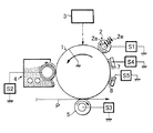
図1は、本発明による、現像手段が転写後の残トナーを回収するクリーナーレス方式の一例を示す。図1において、電子写真感光体1は矢印方向に回転し、帯電手段2により帯電される。その後露光手段3により画像情報が静電潜像として書き込まれ、現像手段4により静電潜像はトナー像として可視像化される。可視像化された感光体表面のトナー像は転写手段5により転写材Pに転写される。この転写工程において、転写されずに感光体表面に残った転写残トナーは、現像剤帯電量制御手段7により上述の帯電と同極性に帯電され、前述の帯電手段2、露光手段3を経て、再度現像に供されるかもしくは現像装置に回収される。
FIG. 1 shows an example of a cleanerless system in which a developing unit collects residual toner after transfer according to the present invention. In FIG. 1, the
本発明においては、上述の電子写真感光体1、帯電手段2、現像手段4及び現像剤帯電量制御手段7などの構成要素のうち、複数のものをプロセスカートリッジとして一体に支持して構成し、このプロセスカートリッジを複写機やレーザービームプリンターなどの電子写真装置本体に対して着脱自在に構成してもよい。
In the present invention, a plurality of components such as the electrophotographic
帯電手段2は、近接帯電のように電子写真感光体に対し非接触で電子写真感光体を帯電させる方法や、電子写真感光体に導電性ローラー、ブラシ、ブレード等を接触させて帯電させる接触帯電方式や注入帯電方式が用いられる。
The
また、露光手段3より照射する画像露光は、電子写真装置が複写機やプリンターである場合には、原稿からの反射光、透過光、又はセンサーで原稿を読みとり信号化しこの信号に従って行われるレーザービームの走査、LEDアレイの駆動、若しくは液晶シャッターアレイの駆動などにより照射される光である。
In addition, when the electrophotographic apparatus is a copying machine or a printer, the image exposure irradiated from the
現像手段4は、ジャンピング現像、2成分接触現像、1成分接触現像などが用いられる。 As the developing means 4, jumping development, two-component contact development, one-component contact development, or the like is used.
現像剤帯電量制御手段7は、固定のブラシ状部材、ブラシ回転体、弾性ローラー体等の形態が挙げられる Examples of the developer charge amount control means 7 include a fixed brush-like member, a brush rotating body, and an elastic roller body.
また、本発明による電子写真装置は、現像剤帯電量制御手段7に加えて、電子写真感光体1表面の残トナーに帯電性を付与する補助装置をさらに有してもよい。図2は、この態様を示す図であって、本発明の画像形成方法を実行する画像形成装置の一例を示す模式図である。図2によると、この態様における電子写真装置は、電子写真感光体1表面に可視像化されたトナー像を転写材Pに転写する転写手段5と、転写されずに感光体表面に残った転写残トナーを上述の帯電と同極性に帯電する現像剤帯電量制御手段7との間に、残留現像剤均一化手段8を有する。残留現像剤均一化手段8は、電子写真感光体1表面の残トナーを均一化するものである。残留現像剤均一化手段8の部材についても、固定のブラシ状部材、ブラシ回転体、弾性ローラー体、シート状部材など任意の形態をとり得る。また、この部材は、感光体に対してその長手方向にスラストさせ、電位付与性をより均一にさせることもできる。さらに接地させても、バイアスを印加してもよい。
In addition to the developer charge amount control means 7, the electrophotographic apparatus according to the present invention may further include an auxiliary device that imparts chargeability to the residual toner on the surface of the electrophotographic
本発明による電子写真感光体は、導電性筒状支持体上に感光層、又は感光層及び保護層を有する電子写真感光体であって、電子写真感光体の表面層の弾性変形率Weが45%以上65%以下であり、初期表面粗さ:Rzjis(十点平均面粗さ)が0.3μm以上1.3μm以下であり、かつ初期最大高さRzが2.0μm未満であることを特徴とする。感光体表面を上記条件に粗面化することにより、画像流れの原因である帯電生成物が上述した補助帯電部材でかき取られやすくなり、感光体表面に帯電生成物が蓄積しないため画像流れを防止することができると推測される。感光体の初期表面粗さが0.3μm未満である場合、画像流れ解消に効果が無く、1.3μmより大きい場合、文字再現性が劣るという問題を生じる場合がある。また、最大高さRzは2.0μm未満が好ましい。2.0μm以上であると、繰り返し使用において補助帯電部材との摺擦により傷として成長し、ハーフトーン画像上に白スジとして現れる問題が生じる。 The electrophotographic photosensitive member according to the present invention is an electrophotographic photosensitive member having a photosensitive layer or a photosensitive layer and a protective layer on a conductive cylindrical support, and the elastic deformation ratio We of the surface layer of the electrophotographic photosensitive member is 45. % To 65%, initial surface roughness: Rzjis (ten-point average surface roughness) is 0.3 μm to 1.3 μm, and initial maximum height Rz is less than 2.0 μm And By roughening the surface of the photoconductor under the above conditions, the charged product that is the cause of image flow can be easily scraped off by the auxiliary charging member described above. It is estimated that it can be prevented. When the initial surface roughness of the photoconductor is less than 0.3 μm, there is no effect in eliminating image blur, and when it is greater than 1.3 μm, there is a problem that character reproducibility is poor. Further, the maximum height Rz is preferably less than 2.0 μm. When the thickness is 2.0 μm or more, there arises a problem that, as it is repeatedly used, it grows as a scratch due to rubbing with the auxiliary charging member and appears as a white stripe on the halftone image.
表面形状の測定法において、本発明において十点平均粗さ(Rzjis)、最大高さ(Rz)はJIS−B0601−2001に記載の方法に準じて測定したものをいう。測定は表面粗さ測定器(商品名:サーフコーダSE3500型、(株)小坂研究所製)を用いて行った。 In the surface shape measurement method, the ten-point average roughness (Rzjis) and the maximum height (Rz) in the present invention are those measured in accordance with the method described in JIS-B0601-2001. The measurement was performed using a surface roughness measuring instrument (trade name: Surfcorder SE3500 type, manufactured by Kosaka Laboratory Ltd.).
また、感光体表面層の弾性変形率は45%以上となると、繰り返し使用後の表面形状の変化が小さくなり、本発明の粗面化がより効果的になる。一方、弾性変形率が65%を超えると、クラックや、瞬間的な外的衝撃により致命的な傷が生じる。 Further, when the elastic deformation rate of the photoreceptor surface layer is 45% or more, the change in the surface shape after repeated use becomes small, and the roughening of the present invention becomes more effective. On the other hand, if the elastic deformation rate exceeds 65%, fatal scratches are caused by cracks or instantaneous external impacts.
さらには、本発明による電子写真感光体の表面層のユニバーサル硬度(HU)は、150以上220N/mm2以下であることが好ましい。150N/mm2未満の場合は、感光体表面の耐磨耗性が十分ではなく、220N/mm2を超える場合は、上述した補助帯電部材との摺擦により傷が発生しやすい。 Furthermore, the universal hardness (HU) of the surface layer of the electrophotographic photoreceptor according to the present invention is preferably 150 or more and 220 N / mm 2 or less. If it is less than 150 N / mm 2, the abrasion resistance of the surface of the photoreceptor is not sufficient, and if it exceeds 220 N / mm 2 , scratches are likely to occur due to rubbing with the auxiliary charging member described above.
弾性変形率及びユニバーサル硬度(HU)は、微小硬さ測定装置フィッシャースコープH100V(Fischer社製)を用いて25℃、湿度50%RHの環境下で対面角136°のビッカース四角錐ダイヤモンド圧子に連続的に6mNの荷重をかけ、荷重下での押し込み深さを直読することにより測定した値である。具体的には、最終荷重6mNまで段階的に(各点0.1秒の保持時間で273点)測定する。弾性変形率は、圧子が膜に対して仕事量(エネルギー)、すなわち圧子の膜に対する荷重の増減によるエネルギーの変化より求めることができ、具体的には弾性変形仕事量Weを全仕事量Wtで除した値である。
弾性変形率=We/Wt
また、ユニバーサル硬度(HU)は、ユニバーサル硬さ値(HU)は、圧子に最終荷重6mNをかけたときの該圧子の押し込み深さから下記式により求めることができる。なお、下記式中、HUはユニバーサル硬さ(HU)を意味し、Ffは最終荷重を意味し、Sfは最終荷重をかけたときの圧子の押し込まれた部分の表面積を意味し、hfは最終荷重をかけたときの圧子の押し込み深さを意味する。
The elastic deformation rate and universal hardness (HU) are continuous with a Vickers square pyramid diamond indenter having a facing angle of 136 ° in an environment of 25 ° C. and humidity 50% RH using a microhardness measuring device Fischerscope H100V (manufactured by Fischer). This is a value measured by applying a load of 6 mN and directly reading the indentation depth under the load. Specifically, measurement is performed stepwise up to a final load of 6 mN (273 points with a holding time of 0.1 seconds for each point). The elastic deformation rate can be obtained from the work (energy) of the indenter with respect to the film, that is, the change in energy due to the increase or decrease of the load on the film of the indenter. Specifically, the elastic deformation work We is defined as the total work Wt. It is the value divided.
Elastic deformation rate = We / Wt
Further, the universal hardness (HU) can be obtained from the following expression from the indentation depth of the indenter when the final load of 6 mN is applied to the indenter. In the following formula, HU means universal hardness (HU), F f means the final load, S f means the surface area of the indented portion when the final load is applied, h f means the indentation depth of the indenter when the final load is applied.

本発明において、電子写真感光体の周面の耐傷性や耐摩耗性を向上させ、本発明の効果が得られやすい電子写真感光体としては、表面層に、加熱又は放射線照射により重合又は架橋し硬化する樹脂を含有することが好ましい。表面層に硬化性樹脂を含有する感光体の製造方法は、塗料中に重合性官能基を有するモノマー又はオリゴマー等を含有させ、製膜、乾燥後、この膜を加熱及び放射線照射等で重合を進行させる工程を有していてもよい。この方法により、3次元的に架橋、硬化することにより溶剤等に不溶、不融の強靭な製膜層を形成するため、表面層の磨耗量を格段に低減させることができ、より繰り返し使用における初期表面粗さの維持が可能となり、長期にわたって本発明の効果を得ることができる。 In the present invention, the electrophotographic photosensitive member that improves the scratch resistance and abrasion resistance of the peripheral surface of the electrophotographic photosensitive member and can easily obtain the effects of the present invention is polymerized or crosslinked on the surface layer by heating or irradiation. It is preferable to contain a resin that cures. The method for producing a photoreceptor containing a curable resin in the surface layer includes a monomer or oligomer having a polymerizable functional group in the paint, and after film formation and drying, the film is polymerized by heating and irradiation. You may have the process to advance. By this method, three-dimensionally cross-linked and cured to form a tough film-forming layer that is insoluble and infusible in solvents, etc., the amount of wear of the surface layer can be significantly reduced, and in repeated use The initial surface roughness can be maintained, and the effects of the present invention can be obtained over a long period of time.
また表面層は、電荷輸送機能を有してもよい。電荷輸送機能を有する場合は感光層の一部として扱い、電荷輸送機能を有していない場合は下記にも述べるとおり保護層(または表面保護層)と称して感光層とは区別している。本発明の最良の構成は、同一分子内に重合性官能基を有する電荷輸送材料を含有する塗料を塗布し製膜後、硬化させて、表面が硬化した感光層を得ることが好ましい。最表面層の硬化層の強度をより高くするために重合性官能基は同一分子内に2つ以上存在することが好ましい。 The surface layer may have a charge transport function. A case having a charge transport function is treated as a part of the photosensitive layer, and a case having no charge transport function is referred to as a protective layer (or surface protective layer) as described below to distinguish it from the photosensitive layer. In the best constitution of the present invention, it is preferable to obtain a photosensitive layer having a hardened surface by applying a coating containing a charge transporting material having a polymerizable functional group in the same molecule, and then curing the coating. In order to further increase the strength of the hardened layer of the outermost surface layer, it is preferable that two or more polymerizable functional groups exist in the same molecule.
感光層の層構成として、導電性支持体側から電荷発生層/電荷輸送層をこの順に積層した順層積層構成、導電性支持体側から電荷輸送層/電荷発生層をこの順に積層した逆層積層構成、または電荷発生材料と電荷輸送材料を同一層中に分散した単層からなる構成の、いずれの構成をとることも可能である。 As the layer structure of the photosensitive layer, a normal layer stack structure in which the charge generation layer / charge transport layer are stacked in this order from the conductive support side, and a reverse layer stack structure in which the charge transport layer / charge generation layer is stacked in this order from the conductive support side. Alternatively, any configuration of a single layer in which the charge generation material and the charge transport material are dispersed in the same layer can be employed.
単層の感光層では光キャリアの生成と移動が同一層内で行なわれ、また感光層そのものが表面層となる。一方積層の感光層では、光キャリアを生成する電荷発生層と生成したキャリアが移動する電荷輸送層とが積層された構成をとる。 In a single photosensitive layer, photocarriers are generated and moved in the same layer, and the photosensitive layer itself is a surface layer. On the other hand, the laminated photosensitive layer has a structure in which a charge generation layer for generating photocarriers and a charge transport layer for moving the generated carriers are laminated.
最も好ましい層構成は、導電性支持体側から電荷発生層/電荷輸送層をこの順に積層した順層構成である。 The most preferable layer structure is a normal layer structure in which the charge generation layer / charge transport layer are laminated in this order from the conductive support side.
この場合、電荷輸送層が硬化性樹脂を含有する一層からなる最表面層である電子写真感光体、又は電荷輸送層が非硬化型の第一層と硬化型の第二層の積層型であり、硬化型の第二層が最表面層である電子写真感光体のいずれかが好ましい。 In this case, the charge transport layer is an electrophotographic photosensitive member that is an outermost surface layer containing a curable resin, or the charge transport layer is a laminated type of a non-curable first layer and a curable second layer. Any of the electrophotographic photoreceptors in which the curable second layer is the outermost surface layer is preferable.
また、単層、積層どちらの場合においても、感光層の上層に保護層を設けることが可能であり、この場合保護層が表面の硬化性樹脂含有層となることが好ましい。 In either case of a single layer or a laminated layer, it is possible to provide a protective layer above the photosensitive layer. In this case, the protective layer is preferably a curable resin-containing layer on the surface.
導電性基体としては、導電性を有するもの(導電性支持体)であればよく、例えば、アルミニウム、ニッケル、銅、金、鉄、アルミニウム合金、ステンレスなどの金属製(合金製)の支持体であってもよい。また、アルミニウム、アルミニウム合金、酸化インジウム−酸化スズ合金などを真空蒸着することによって形成された被膜からなる層を有する上記金属製支持体やプラスチック(ポリエステル樹脂やポリカーボネート樹脂やポリイミド樹脂など)製支持体やガラス製支持体を用いることもできる。また、カーボンブラック、酸化スズ粒子、酸化チタン粒子、銀粒子などの導電性粒子を適当な結着樹脂と共にプラスチックや紙に含浸した支持体や、導電性結着樹脂を有するプラスチック製の支持体などを用いることもできる。また、支持体の形状としては、円筒状、ベルト状などが挙げられるが、円筒状が好ましい。 The conductive substrate may be any conductive substrate (conductive support), for example, a metal (alloy) support such as aluminum, nickel, copper, gold, iron, aluminum alloy, and stainless steel. There may be. Also, the above-mentioned metal support or plastic (polyester resin, polycarbonate resin, polyimide resin, etc.) support having a layer formed of a film formed by vacuum deposition of aluminum, aluminum alloy, indium oxide-tin oxide alloy, or the like. A glass support can also be used. In addition, a support in which conductive particles such as carbon black, tin oxide particles, titanium oxide particles, and silver particles are impregnated into plastic or paper together with an appropriate binder resin, or a plastic support having a conductive binder resin, etc. Can also be used. In addition, examples of the shape of the support include a cylindrical shape and a belt shape, and a cylindrical shape is preferable.
支持体の表面は、レーザー光などの散乱による干渉縞の防止などを目的として、切削処理、粗面化処理(ホーニング処理やブラスト処理など)、アルマイト処理などを施してもよい。また、アルカリリン酸塩やリン酸やタンニン酸を主成分とする酸性水溶液に金属塩の化合物またはフッ素化合物の金属塩を溶解してなる溶液で化学処理を施してもよい。 The surface of the support may be subjected to a cutting process, a roughening process (such as a honing process or a blasting process), an alumite process, or the like for the purpose of preventing interference fringes due to scattering of laser light or the like. Alternatively, chemical treatment may be performed with a solution obtained by dissolving a metal salt compound or a fluorine compound metal salt in an acidic aqueous solution mainly composed of alkali phosphate, phosphoric acid, or tannic acid.
ホーニング処理としては、乾式ホーニング処理と湿式ホーニング処理とがある。湿式ホーニング処理は、水などの液体に粉末状の研磨剤を懸濁させ、高速度で支持体の表面に吹き付けて支持体の表面を粗面化する方法であり、表面粗さは、吹き付け圧力、速度、研磨剤の量、種類、形状、大きさ、硬度、比重および懸濁温度などによって制御することができる。乾式ホーニング処理は、研磨剤をエアーによって高速度で支持体の表面に吹き付けて支持体の表面を粗面化する方法であり、湿式ホーニング処理と同じように表面粗さを制御することができる。ホーニング処理に用いられる研磨剤としては、炭化ケイ素、アルミナ、鉄、ガラスビーズなどの粒子が挙げられる。 The honing process includes a dry honing process and a wet honing process. The wet honing treatment is a method in which a powdery abrasive is suspended in a liquid such as water and sprayed onto the surface of the support at a high speed to roughen the surface of the support, and the surface roughness is determined by the spray pressure. , Speed, amount of abrasive, type, shape, size, hardness, specific gravity, suspension temperature and the like. The dry honing treatment is a method of roughening the surface of the support by spraying an abrasive on the surface of the support with air at a high speed, and the surface roughness can be controlled in the same manner as the wet honing treatment. As an abrasive | polishing agent used for a honing process, particles, such as a silicon carbide, an alumina, iron, a glass bead, are mentioned.
支持体と感光層又は後述の中間層との間には、レーザー光などの散乱による干渉縞の防止や、支持体の傷の被覆を目的とした導電層を設けてもよい。 Between the support and the photosensitive layer or an intermediate layer described later, a conductive layer may be provided for the purpose of preventing interference fringes due to scattering of laser light or the like and covering the scratches on the support.
導電層は、カーボンブラック、金属粒子、金属酸化物粒子などの導電性粒子を結着樹脂に分散させて形成することができる。好適な金属酸化物粒子としては、酸化亜鉛や酸化チタンの粒子が挙げられる。また、導電性粒子として、硫酸バリウムの粒子を用いることもできる。導電性粒子には、被覆層を設けてもよい。 The conductive layer can be formed by dispersing conductive particles such as carbon black, metal particles, and metal oxide particles in a binder resin. Suitable metal oxide particles include zinc oxide and titanium oxide particles. Also, barium sulfate particles can be used as the conductive particles. A conductive layer may be provided on the conductive particles.
導電性粒子の体積抵抗率は0.1以上1000Ω・cm以下の範囲が好ましく、特には1以上1000Ω・cm以下の範囲がより好ましい。なお、この体積抵抗率は、49MPaの圧力で固めてコイン状としたものを測定サンプルとし、三菱油化(株)製の抵抗測定装置ロレスタAPを用いて測定して求めた値である。導電性粒子の平均粒径は0.05以上1.0μm以下の範囲が好ましく、特には0.07以上0.7μm以下の範囲がより好ましい(この平均粒径は、遠心沈降法により測定した値である。)。導電層中の導電性粒子の割合は、導電層全質量に対して1.0以上90質量%以下の範囲が好ましく、5.0以上80質量%以下の範囲がより好ましい。 The volume resistivity of the conductive particles is preferably in the range of 0.1 to 1000 Ω · cm, and more preferably in the range of 1 to 1000 Ω · cm. The volume resistivity is a value obtained by measurement using a resistance measuring apparatus Loresta AP manufactured by Mitsubishi Oil Chemical Co., Ltd., with a measurement sample that is hardened with a pressure of 49 MPa and formed into a coin shape. The average particle diameter of the conductive particles is preferably in the range of 0.05 to 1.0 μm, more preferably in the range of 0.07 to 0.7 μm (this average particle diameter is a value measured by a centrifugal sedimentation method). .) The ratio of the conductive particles in the conductive layer is preferably in the range of 1.0 to 90% by mass and more preferably in the range of 5.0 to 80% by mass with respect to the total mass of the conductive layer.
導電層に用いられる結着樹脂としては、例えば、フェノール樹脂、ポリウレタン樹脂、ポリアミド樹脂、ポリイミド樹脂、ポリアミドイミド樹脂、ポリアミド酸樹脂、ポリビニルアセタール樹脂、エポキシ樹脂、アクリル樹脂、メラミン樹脂、ポリエステル樹脂などが挙げられる。これらの樹脂は、単独若しくは2種以上の混合物、又はこれらの共重合体として用いることができる。これらの樹脂/混合物/共重合体は、支持体に対する接着性が良好であるとともに、導電性粒子の分散性を向上させ、かつ、成膜後の耐溶剤性が良好である。これらの中でも、フェノール樹脂、ポリウレタン樹脂、ポリアミド酸樹脂が好ましい。 Examples of the binder resin used for the conductive layer include phenol resin, polyurethane resin, polyamide resin, polyimide resin, polyamideimide resin, polyamic acid resin, polyvinyl acetal resin, epoxy resin, acrylic resin, melamine resin, and polyester resin. Can be mentioned. These resins can be used alone or as a mixture of two or more thereof, or a copolymer thereof. These resins / mixtures / copolymers have good adhesion to the support, improve the dispersibility of the conductive particles, and have good solvent resistance after film formation. Among these, a phenol resin, a polyurethane resin, and a polyamic acid resin are preferable.
導電層の膜厚は0.1以上30μm以下であることが好ましく、0.5以上20μm以下であることがより好ましい。 The thickness of the conductive layer is preferably from 0.1 to 30 μm, more preferably from 0.5 to 20 μm.
導電層の体積抵抗率は1013Ω・cm以下であることが好ましく、105以上1012Ω・cm以下の範囲であることがより好ましい。なお、この体積抵抗率は、測定対象の導電層と同じ材料によってアルミニウム板上に被膜を形成し、この皮膜上に金の薄膜を形成して、アルミニウム板と金薄膜の両電極間を流れる電流値をpAメーターで測定して求めた値である。 The volume resistivity of the conductive layer is preferably 10 13 Ω · cm or less, and more preferably in the range of 10 5 or more and 10 12 Ω · cm or less. The volume resistivity is determined by forming a film on the aluminum plate with the same material as the conductive layer to be measured, forming a gold thin film on the film, and flowing between the electrodes of the aluminum plate and the gold thin film. It is a value obtained by measuring the value with a pA meter.
また、導電層は、必要に応じて、フッ素、又はアンチモンを有してもよいし、導電層の表面性を高めるために、レベリング剤を添加してもよい。 In addition, the conductive layer may contain fluorine or antimony as necessary, and a leveling agent may be added to improve the surface property of the conductive layer.
支持体又は導電層と感光層との間には、バリア機能や接着機能を有する中間層(下引き層、接着層とも呼ばれる。)を設けてもよい。中間層は、感光層の接着性改良、塗工性改良、支持体からの電荷注入性改良、感光層の電気的破壊に対する保護などのために形成される。 An intermediate layer (also referred to as an undercoat layer or an adhesive layer) having a barrier function or an adhesive function may be provided between the support or the conductive layer and the photosensitive layer. The intermediate layer is formed for the purpose of improving the adhesion of the photosensitive layer, improving the coating property, improving the charge injection property from the support, and protecting the photosensitive layer from electrical breakdown.
中間層は、アクリル樹脂、アリル樹脂、アルキッド樹脂、エチルセルロース樹脂、エチレン−アクリル酸コポリマー、エポキシ樹脂、カゼイン樹脂、シリコーン樹脂、ゼラチン樹脂、ポリアミド、フェノール樹脂、ブチラール樹脂、ポリアクリレート樹脂、ポリアセタール樹脂、ポリアミドイミド樹脂、ポリアミド樹脂、ポリアリルエーテル樹脂、ポリイミド樹脂、ポリウレタン樹脂、ポリエステル樹脂、ポリエチレン樹脂、ポリカーボネート樹脂、ポリスチレン樹脂、ポリスルホン樹脂、ポリビニルアルコール樹脂、ポリブタジエン樹脂、ポリプロピレン樹脂、ユリア樹脂などの樹脂や、酸化アルミニウムなどの材料を用いて形成することができる。 The intermediate layer is acrylic resin, allyl resin, alkyd resin, ethyl cellulose resin, ethylene-acrylic acid copolymer, epoxy resin, casein resin, silicone resin, gelatin resin, polyamide, phenol resin, butyral resin, polyacrylate resin, polyacetal resin, polyamide Imide resin, polyamide resin, polyallyl ether resin, polyimide resin, polyurethane resin, polyester resin, polyethylene resin, polycarbonate resin, polystyrene resin, polysulfone resin, polyvinyl alcohol resin, polybutadiene resin, polypropylene resin, urea resin, etc. It can be formed using a material such as aluminum.
中間層の膜厚は0.05以上5μm以下であることが好ましく、特には0.3以上1μm以下であることがより好ましい。 The thickness of the intermediate layer is preferably from 0.05 to 5 μm, and more preferably from 0.3 to 1 μm.
本発明の感光層が機能分離型の感光層の層構成である場合、電荷発生層及び電荷輸送層を積層する。しかしながら、成膜する順序は特に制限されるものではない。 When the photosensitive layer of the present invention has a layer structure of a function-separated type photosensitive layer, a charge generation layer and a charge transport layer are laminated. However, the order of film formation is not particularly limited.
本発明において電荷発生材料としては一般的な材料を用いることが可能である。電荷発生材料は、本技術分野公知の種々の材料を用い得るが、例えば、セレン−テルル、ピリリウム、チアピリリウム系染料、各種の中心金属を有する化合物又は結晶系があげられ、具体的には例えばα、β、γ、εおよびX型などの結晶型を有するフタロシアニン化合物、アントアントロン顔料、ジベンズピレンキノン顔料、ピラントロン顔料、トリスアゾ顔料、ジスアゾ顔料、モノアゾ顔料、インジゴ顔料、キナクリドン顔料、非対称キノシアニン顔料、キノシアニン、A−Si(アモルファスシリコン)等が挙げられる。 In the present invention, a general material can be used as the charge generation material. Various materials known in the art can be used as the charge generating material, and examples thereof include selenium-tellurium, pyrylium, thiapyrylium dyes, compounds having various central metals, and crystal systems. , Phthalocyanine compounds having crystal types such as β, γ, ε, and X type, anthanthrone pigments, dibenzpyrenequinone pigments, pyranthrone pigments, trisazo pigments, disazo pigments, monoazo pigments, indigo pigments, quinacridone pigments, asymmetric quinocyanine pigments, Examples include quinocyanine and A-Si (amorphous silicon).
また、電荷発生材料以外に、バインダー樹脂を用いることも可能である。バインダー樹脂の具体例として、ポリエステル、ポリウレタン、ポリアクリレート、ポリエチレン、ポリスチレン、ポリブタジエン、ポリカーボネート、ポリアミド、ポリプロピレン、ポリイミド、フェノール樹脂、アクリル樹脂、シリコーン樹脂、エポキシ樹脂、ユリア樹脂、アリル樹脂、アルキッド樹脂、ポリアミド−イミド、ポリサルフォン、ポリアリルエーテル、ポリアセタール、ブチラール樹脂、ベンザール樹脂などが挙げられる。 In addition to the charge generation material, a binder resin can also be used. Specific examples of the binder resin include polyester, polyurethane, polyacrylate, polyethylene, polystyrene, polybutadiene, polycarbonate, polyamide, polypropylene, polyimide, phenol resin, acrylic resin, silicone resin, epoxy resin, urea resin, allyl resin, alkyd resin, polyamide. -Imido, polysulfone, polyallyl ether, polyacetal, butyral resin, benzal resin and the like.
電荷発生層にバインダー樹脂を含有する場合、電荷発生材料とバインダー樹脂の比率は、バインダー樹脂と電荷発生材料との総量に対する電荷発生材料の質量比で、0.1以上100%以下が好ましく、より好ましくは10以上80%以下である。 When the charge generation layer contains a binder resin, the ratio of the charge generation material to the binder resin is preferably 0.1 to 100% in terms of the mass ratio of the charge generation material to the total amount of the binder resin and the charge generation material. Preferably, it is 10 to 80%.
電荷発生層の膜厚は、0.001以上6μm以下が好ましく、より好ましくは、0.01以上2μm以下である。電荷発生層全体に含有される電荷発生材料の質量比は、10以上100%以下が好ましく、より好ましくは50以上100%以下である。 The thickness of the charge generation layer is preferably from 0.001 to 6 μm, more preferably from 0.01 to 2 μm. The mass ratio of the charge generation material contained in the entire charge generation layer is preferably 10 or more and 100% or less, more preferably 50 or more and 100% or less.
電荷輸送材料の例としては、ピレン化合物、N−アルキルカルバゾール化合物、ヒドラゾン化合物、N,N−ジアルキルアニリン化合物、ジフェニルアミン化合物、トリフェニルアミン化合物、トリフェニルメタン化合物、ピラゾリン化合物、スチリル化合物、スチルベン化合物などが挙げられる。 Examples of charge transport materials include pyrene compounds, N-alkylcarbazole compounds, hydrazone compounds, N, N-dialkylaniline compounds, diphenylamine compounds, triphenylamine compounds, triphenylmethane compounds, pyrazoline compounds, styryl compounds, stilbene compounds, etc. Is mentioned.
また、電荷輸送材料以外に、バインダー樹脂を用いることも可能である。バインダー樹脂の具体例として、ポリエステル、ポリウレタン、ポリアクリレート、ポリエチレン、ポリスチレン、ポリブタジエン、ポリカーボネート、ポリアミド、ポリプロピレン、ポリイミドなどが挙げられる。 In addition to the charge transport material, a binder resin can also be used. Specific examples of the binder resin include polyester, polyurethane, polyacrylate, polyethylene, polystyrene, polybutadiene, polycarbonate, polyamide, polypropylene, polyimide, and the like.
電荷輸送層を最表面に用いる場合、電荷輸送層に熱、光又は放射線照射等を利用して、硬化・重合する樹脂、若しくはモノマー、又は正孔輸送機能を有するこれらの樹脂若しくはモノマーを用い得る。 When the charge transport layer is used on the outermost surface, a resin or monomer that cures or polymerizes by using heat, light, radiation irradiation, or the like, or these resins or monomers having a hole transport function can be used for the charge transport layer. .
熱、光又は放射線照射により重合又は架橋し硬化する化合物としては、熱による加水分解や縮合反応を経由して架橋するものとしてフェノール系、エポキシ系、アルコキシシラン系など、熱や光又は放射線照射によりラジカル等の活性点を発生させ、重合又は架橋することが可能な化合物であれば限定されないが、反応性や強度の点で、一般的には連鎖重合性官能基を有する化合物が挙げられる。なかでも、反応性の高さ、反応速度の速さ、材料の汎用性等の点で、分子内に不飽和重合性官能基を有する化合物が好ましく、不飽和重合性官能基としてアクリロイルオキシ基、メタクリロイルオキシ基、スチレン基等が特に好ましい。これらの化合物は、モノマー、オリゴマー、マクロマー、ポリマーのいずれにも限定されることなく、適宜選択し、或いは組み合わせて用いてもよい。また、電荷輸送性、好ましくは正孔輸送性を有し、且つ熱、光又は放射線照射により重合又は架橋し硬化する化合物を用いる場合、それ単独で電荷輸送層を形成することができ、この場合、特に電子写真特性に優れ且つ高強度な表面層を形成することが可能となる。また、本発明による表面層は、電荷輸送材料、及び電荷輸送性を有さない熱、光又は放射線照射により重合又は架橋し硬化する化合物をさらに有してもよい。 As a compound that is polymerized or crosslinked and cured by irradiation with heat, light, or radiation, it can be crosslinked via a hydrolysis or condensation reaction by heat, such as phenol, epoxy, alkoxysilane, etc. by irradiation with heat, light, or radiation. Although it will not be limited if it is a compound which can generate | occur | produce active sites, such as a radical, and can superpose | polymerize or bridge | crosslink, the compound which has a chain polymerizable functional group is generally mentioned in the point of reactivity or intensity | strength. Among them, a compound having an unsaturated polymerizable functional group in the molecule is preferable in terms of high reactivity, fast reaction rate, versatility of materials, etc., and an acryloyloxy group as the unsaturated polymerizable functional group, A methacryloyloxy group, a styrene group and the like are particularly preferable. These compounds are not limited to monomers, oligomers, macromers, and polymers, and may be appropriately selected or used in combination. In addition, in the case of using a compound having charge transporting property, preferably hole transporting property, and being polymerized or crosslinked and cured by irradiation with heat, light or radiation, a charge transport layer can be formed by itself. In particular, a surface layer having excellent electrophotographic characteristics and high strength can be formed. In addition, the surface layer according to the present invention may further include a charge transporting material and a compound that is polymerized or crosslinked and cured by irradiation with heat, light, or radiation that does not have charge transporting properties.
電荷輸送性を有し、且つ熱、光又は放射線照射により重合又は架橋し硬化する化合物は、例えば不飽和重合性官能基を有する公知の正孔輸送性化合物や、公知の正孔輸送性化合物の一部に不飽和重合性官能基を付加した化合物が用いられる。公知の正孔輸送性化合物の例としてはヒドラゾン化合物、ピラゾリン化合物、トリフェニルアミン化合物、ベンジジン化合物、スチルベン化合物等が挙げられるが、正孔輸送性化合物であればいかなる化合物も使用可能である。さらに、本発明において電子写真感光体表面層の硬度を十分に確保するためには、不飽和重合性官能基を有する化合物は一分子中に複数の不飽和重合性官能基を有する化合物であることが好ましい。 The compound having charge transporting property and polymerized or crosslinked and cured by irradiation with heat, light or radiation is, for example, a known hole transporting compound having an unsaturated polymerizable functional group or a known hole transporting compound. A compound in which an unsaturated polymerizable functional group is partially added is used. Examples of known hole transporting compounds include hydrazone compounds, pyrazoline compounds, triphenylamine compounds, benzidine compounds, stilbene compounds and the like, but any compounds can be used as long as they are hole transporting compounds. Furthermore, in the present invention, in order to sufficiently ensure the hardness of the electrophotographic photoreceptor surface layer, the compound having an unsaturated polymerizable functional group is a compound having a plurality of unsaturated polymerizable functional groups in one molecule. Is preferred.
電荷輸送層にバインダー樹脂を含有する場合、電荷輸送材料とバインダー樹脂との比率は、バインダー樹脂と電荷輸送材料との総量に対する電荷輸送材料の質量比で0.1以上100%以下が好ましく、より好ましくは10以上80%以下である。 When the charge transport layer contains a binder resin, the ratio of the charge transport material to the binder resin is preferably 0.1 to 100% by mass ratio of the charge transport material to the total amount of the binder resin and the charge transport material, Preferably, it is 10 to 80%.
電荷輸送層の厚さは、5以上40μm以下が好ましく、より好ましくは10以上30μm以下である。この厚さが5μm未満であると帯電能が保てず、40μmよりも大きいと残留電位が高くなりすぎる。 The thickness of the charge transport layer is preferably from 5 to 40 μm, more preferably from 10 to 30 μm. If this thickness is less than 5 μm, the charging ability cannot be maintained, and if it is greater than 40 μm, the residual potential becomes too high.
電荷輸送層中に含まれる電荷輸送材料の量は、質量比で、好ましくは20以上100%以下であり、より好ましくは30以上90%以下である。 The amount of the charge transport material contained in the charge transport layer is preferably 20 or more and 100% or less, and more preferably 30 or more and 90% or less in mass ratio.
感光層を単層で用いる場合、電荷発生材料と電荷輸送材料を同一層内に含有する。電荷発生材料及び電荷輸送材料の具体例は、上述の積層感光体の場合と同様である。同様に放射線を利用して、硬化・重合する樹脂、若しくはモノマー、又は正孔輸送機能を有するこれらの樹脂若しくはモノマーを用い得る。 When the photosensitive layer is used as a single layer, the charge generation material and the charge transport material are contained in the same layer. Specific examples of the charge generation material and the charge transport material are the same as in the case of the above-described laminated photoreceptor. Similarly, a resin or monomer that cures or polymerizes using radiation, or a resin or monomer having a hole transport function may be used.
単層感光層の厚さは、8以上40μm以下が好ましく、より好ましくは12以上30μm以下である。単層感光層は、電荷発生材料や電荷輸送材料等の光導電性材料を20以上100質量%以下有することが好ましく、より好ましくは30以上90質量%以下である。 The thickness of the single photosensitive layer is preferably from 8 to 40 μm, more preferably from 12 to 30 μm. The single-layer photosensitive layer preferably has a photoconductive material such as a charge generation material or a charge transport material in the range of 20 to 100% by mass, and more preferably 30 to 90% by mass.
最表面に保護層を設ける場合、その膜厚は0.01以上10μm以下が好ましく、より好ましくは0.1以上7μm以下である。放射線を利用して、硬化・重合する樹脂、若しくはモノマー、又は正孔輸送機能を有するこれらの樹脂若しくはモノマーを用い得る。更に、保護層中に金属若しくはその酸化物、窒化物、塩、合金又はカーボン等の導電性材料を含有してもよい。その様な金属種としては、鉄、銅、金、銀、鉛、亜鉛、ニッケル、スズ、アルミニウム、チタン、アンチモン、インジウムなどが挙げられ、具体的には、ITO、TiO2、ZnO、SnO2、Al2O3などが使用可能である。導電性材料は微粒子状のものを保護層中に分散させるが、その粒子径は、好ましくは0.001以上5μm以下、より好ましくは0.01以上1μm以下のものが用いられ、その保護層への添加量は、好ましくは1以上70質量%以下、より好ましくは5以上50質量%以下である。分散剤としてチタンカップリング剤、シランカップリング剤、各種界面活性などを用いてもよい。 When providing a protective layer on the outermost surface, the film thickness is preferably 0.01 to 10 μm, more preferably 0.1 to 7 μm. Resins that cure or polymerize using radiation, or monomers, or these resins or monomers having a hole transport function can be used. Furthermore, you may contain electroconductive materials, such as a metal or its oxide, nitride, salt, an alloy, or carbon, in a protective layer. Examples of such metal species include iron, copper, gold, silver, lead, zinc, nickel, tin, aluminum, titanium, antimony, and indium. Specifically, ITO, TiO 2 , ZnO, SnO 2 Al 2 O 3 or the like can be used. The conductive material is dispersed in the protective layer in the form of fine particles, and the particle diameter is preferably 0.001 to 5 μm, more preferably 0.01 to 1 μm. Is preferably 1 or more and 70% by mass or less, more preferably 5 or more and 50% by mass or less. A titanium coupling agent, a silane coupling agent, various surface activities, and the like may be used as the dispersant.
感光層を構成する各層には、酸化防止剤や光劣化防止剤等各種添加剤を用いてもよい。また、表面層にはその滑性や撥水性を改善する目的で各種フッ素化合物やシラン化合物、金属酸化物等あるいはそれらの微粒子等を含有してもよい。これらの分散性を改善する目的で分散剤や界面活性剤を用いてもよい。表面層におけるこれら添加物の含有量は好ましくは1以上70質量%以下、より好ましくは5以上50質量%以下である。 Various additives such as an antioxidant and a photodegradation inhibitor may be used for each layer constituting the photosensitive layer. Further, the surface layer may contain various fluorine compounds, silane compounds, metal oxides or the like or fine particles thereof for the purpose of improving the lubricity and water repellency. A dispersant or a surfactant may be used for the purpose of improving these dispersibility. The content of these additives in the surface layer is preferably 1 to 70% by mass, more preferably 5 to 50% by mass.
本発明の電子写真感光体の製造方法としては、蒸着、塗布などの方法が用いられるが、なかでも塗布法が最も好ましい。塗布による方法は、薄膜から厚膜まで広い範囲で、しかもさまざまな組成の膜が形成可能である。具体的には、バーコーター、ナイフコーター、浸漬塗布、スプレー塗布、ビーム塗布、静電塗布、ロールコーター、アトライター、粉体塗布などで塗布される。 As a method for producing the electrophotographic photoreceptor of the present invention, methods such as vapor deposition and coating are used, and among these, the coating method is most preferable. The coating method can form films having various compositions in a wide range from a thin film to a thick film. Specifically, it is applied by a bar coater, knife coater, dip coating, spray coating, beam coating, electrostatic coating, roll coater, attritor, powder coating or the like.
次に表面層を重合又は架橋して化合物を硬化させて形成する方法について説明する。本発明において表面層の形成は、熱、光又は放射線照射により、重合又は架橋し硬化する化合物を用いるが、熱又は光による硬化又は架橋反応による場合は、反応開始材を必要とするが、放射線照射の場合には、開始材を必要としないため、電子写真特性の点で、特に好ましい。 Next, a method for forming the surface layer by polymerizing or crosslinking and curing the compound will be described. In the present invention, the formation of the surface layer uses a compound that is polymerized or crosslinked and cured by irradiation with heat, light, or radiation. However, in the case of curing or crosslinking reaction with heat or light, a reaction initiator is required, but radiation is used. In the case of irradiation, since no starting material is required, it is particularly preferable in terms of electrophotographic characteristics.
放射線照射について説明する。本発明における放射線とは、特許文献1の開示と同様に、電子線及びγ線等が挙げられ、装置の大きさ、安全性、コスト、汎用性等、種々の点から、電子線が好ましい。電子線照射をする場合、加速器としては、スキャニング型、エレクトロカーテン型、ブロードビーム型、パルス型及びラミナー型等が挙げられる。
The radiation irradiation will be described. Examples of the radiation in the present invention include an electron beam and a γ-ray as in the disclosure of
電子線照射を用いて本発明による電子写真感光体を形成する場合、電子写真感光体の電気特性及び耐久性能を十分に発現させる上で、電子線の加速電圧は、300KV以下が好ましく、150KV以下がより好ましい。また、電子線の吸収線量は、1以上100Mrad以下(1×10⁴以上1MGy以下)が好ましく、1以上50Mrad以下(5×10⁵Gy)がより好ましい。加速電圧が300KVを超えたり、線量が100Mrad(1MGy)を超えると、電子写真感光体への劣化が起こりやすい。また、本発明による電子線照射を用いた電子写真感光体の形成方法は、重合、架橋の効率をあげるため、加熱工程をさらに有してもよい。 When the electrophotographic photoreceptor according to the present invention is formed using electron beam irradiation, the acceleration voltage of the electron beam is preferably 300 KV or less, and 150 KV or less, in order to sufficiently develop the electrical characteristics and durability of the electrophotographic photoreceptor. Is more preferable. The absorbed dose of the electron beam is preferably 1 or more and 100 Mrad or less (1 × 10 4 or more and 1 MGy or less), and more preferably 1 or more and 50 Mrad or less (5 × 10 5 Gy). When the acceleration voltage exceeds 300 KV or the dose exceeds 100 Mrad (1 MGy), the electrophotographic photosensitive member tends to deteriorate. In addition, the method for forming an electrophotographic photoreceptor using electron beam irradiation according to the present invention may further include a heating step in order to increase the efficiency of polymerization and crosslinking.
本発明による電子写真感光体の好ましい表面形状としては、円周方向に形成された溝と平坦部とを組合せた形状又はディンプル形状が挙げられる。 A preferable surface shape of the electrophotographic photosensitive member according to the present invention includes a shape in which grooves formed in the circumferential direction and a flat portion are combined or a dimple shape.
溝と平坦部とを組み合わせた形状において、この溝の幅は、0.5以上40μm以下で、単位長さ1000μm当たりの溝本数密度が20以上1000以下であることが好ましい。この幅が40μmを超えると、ハーフトーン画像上で白いスジ画像を生じやすい。また、溝本数密度が20未満であると、電子写真感光体の圧接部に不具合を生じ、具体的には、帯電手段の汚れ、現像手段中の現像剤の帯電性劣化、転写手段の傷等が発生する。また、溝本数密度が1000を越えると文字再現性が劣る傾向がある。 In the shape in which the groove and the flat portion are combined, the width of the groove is preferably 0.5 to 40 μm, and the groove number density per unit length of 1000 μm is preferably 20 to 1000. When this width exceeds 40 μm, a white streak image tends to be generated on the halftone image. Further, if the groove number density is less than 20, problems occur in the pressure contact portion of the electrophotographic photosensitive member, specifically, contamination of the charging unit, deterioration of the charging property of the developer in the developing unit, scratches on the transfer unit, etc. Occurs. Further, if the groove density exceeds 1000, the character reproducibility tends to be inferior.
なお、電子写真感光体表面の溝幅、平坦部の幅及び溝本数密度は、非接触3次元表面測定機(商品名:マイクロマップ557N、(株)菱化システム製)を用いて測定を行った。マイクロマップの光学顕微鏡部に5倍の二光束干渉対物レンズを装着し感光体をレンズ下に固定し、表面形状画像をWaveモードでCCDカメラを用いて干渉像を垂直走査させて3次元画像を得る。得た画像の範囲は1.6mm×1.2mmである。このようにして得た画像を解析し、データとして単位長さ1000μm当たりの溝数、溝幅が得られる。このデータを基に、上述の溝幅、溝数の解析が可能となる。なお、本発明においては、溝は、幅0.5μm以上のものをカウントし、電子写真母線方向の3箇所で、それぞれの個所で円周方向について12箇所を測定個所とした。また、溝幅、溝数に関しては、マイクロマップ以外にも市販のレーザー顕微鏡(超深度形状測定顕微鏡VK−8550、VK−9000((株)キーエンス製)、走査型共焦点レーザー顕微鏡OLS3000(オリンパス(株)製)リアルカラーコンフォーカル顕微鏡オプリテクスC130(レーザーテック(株)製))、デジタルマイクロスコープVHX−100、VH−8000((株)キーエンス製))等により、感光体表面画像を得、それを基に画像処理ソフト(例えばWinROOF(三谷商事(株)製)を用い溝幅、溝数を求めることが可能である。また3次元非接触形状測定装置(NewView5032(ザイゴ(株)製))等を用いればマイクロマップと同様に測定することが可能である。 Note that the groove width, flat portion width, and groove number density on the surface of the electrophotographic photosensitive member were measured using a non-contact three-dimensional surface measuring machine (trade name: Micromap 557N, manufactured by Ryoka System Co., Ltd.). It was. Attach a five-fold two-beam interference objective lens to the optical microscope section of the micromap, fix the photoconductor under the lens, and vertically scan the interference image using a CCD camera in the Wave mode to obtain a three-dimensional image. obtain. The range of the obtained image is 1.6 mm × 1.2 mm. The image thus obtained is analyzed, and the number of grooves and the groove width per unit length of 1000 μm are obtained as data. Based on this data, the above-described groove width and number of grooves can be analyzed. In the present invention, grooves having a width of 0.5 μm or more were counted, and at three locations in the electrophotographic bus direction, 12 locations were measured in the circumferential direction at each location. Further, regarding the groove width and the number of grooves, in addition to the micromap, commercially available laser microscopes (ultra-deep shape measurement microscopes VK-8550, VK-9000 (manufactured by Keyence Corporation), scanning confocal laser microscope OLS3000 (Olympus ( Co., Ltd.) Real Color Confocal Microscope Oplitex C130 (Lasertec Co., Ltd.)), Digital Microscope VHX-100, VH-8000 (Keyence Co., Ltd.)) etc. Based on the image processing software (for example, WinROOF (manufactured by Mitani Shoji Co., Ltd.)), the groove width and the number of grooves can be obtained, and a three-dimensional non-contact shape measuring device (NewView 5032 (manufactured by Zygo Co., Ltd.)) It is possible to measure in the same manner as the micromap.
上述の電子写真感光体表面の形状を得るための粗面化方法は、電子写真感光体の表面を物理的に研磨する方法が挙げられるが、その他の方法として、粗面化された支持体上に感光層/保護層を塗布して支持体の表面形状を感光体表面まで維持させる方法や、感光層/保護層を塗布しこれを乾燥する前又は硬化する前に生じる流動性のある状態で、粗面化手段により、上述の表面形状を形成する方法なども挙げられる。粗面化手段の一例としては、研磨砥粒を結着樹脂に分散した研磨シートに電子写真感光体を回転させながら押し当て、感光体表面を研磨する方法が挙げられる。この研磨は、基本的に、未処理の研磨シートを感光体表面に常時圧接し、感光体表面を粗面化することで行われる。この研磨シートは、基本的には絶縁性であるので、シートの接する部位をアースに接地したもの、又は導電性を有するものを用いることが好ましい。本発明における感光体表面の形状は、例えば粗面化手段として研磨シートを用いる場合、研磨シートの送りスピード、感光体と研磨シートの押し当て圧、研磨砥粒の粒径、形状、研磨シートに分散される研磨砥粒の番手、研磨シートの結着樹脂厚、基材厚等を適宜選択することにより、調整すればよい。 Examples of the roughening method for obtaining the shape of the surface of the electrophotographic photosensitive member include a method of physically polishing the surface of the electrophotographic photosensitive member. A method of applying a photosensitive layer / protective layer to maintain the surface shape of the support up to the surface of the photosensitive member, or a fluid state that occurs before the photosensitive layer / protective layer is applied and dried or cured. Moreover, the method of forming the above-mentioned surface shape with a roughening means is also mentioned. As an example of the roughening means, there is a method of polishing the surface of the photoreceptor by pressing the electrophotographic photoreceptor against a polishing sheet in which abrasive grains are dispersed in a binder resin while rotating the electrophotographic photoreceptor. This polishing is basically performed by constantly pressing an untreated polishing sheet against the surface of the photoconductor to roughen the surface of the photoconductor. Since this polishing sheet is basically insulative, it is preferable to use a sheet in which a portion in contact with the sheet is grounded or a conductive sheet. The shape of the photoreceptor surface in the present invention is, for example, when a polishing sheet is used as a roughening means, the polishing sheet feed speed, the pressing pressure between the photoreceptor and the polishing sheet, the grain size and shape of the abrasive grains, and the polishing sheet What is necessary is just to adjust by selecting suitably the count of the abrasive grain to disperse | distribute, the binder resin thickness of a polishing sheet, a base material thickness, etc.
一方、本発明の電子写真感光体は、本発明の課題を達成するために、電子写真感光体の表面にディンプル形状を有することが好ましい。本発明において、このディンプル形状とは、微細な凹凸形状をいう。特に、このディンプル形状は、粗面化する前の基準面よりも凹み多くを持つように加工された表面であることが好ましい。本発明の感光体に適したディンプルの個数は、10000μm2当たり5個以上40個以下が好ましい。好ましいディンプルの面積率は、3以上50%以下が好ましい。これらディンプルの個数や面積率が上限を上回っても、下限を下回っても粗面化した効果が得られ難くなる。 On the other hand, the electrophotographic photoreceptor of the present invention preferably has a dimple shape on the surface of the electrophotographic photoreceptor in order to achieve the object of the present invention. In the present invention, the dimple shape means a fine uneven shape. In particular, the dimple shape is preferably a surface processed so as to have more dents than the reference surface before roughening. The number of dimples suitable for the photoreceptor of the present invention is preferably 5 or more and 40 or less per 10,000 μm 2 . The area ratio of dimples is preferably 3 to 50%. Even if the number and area ratio of these dimples exceed the upper limit or less than the lower limit, it is difficult to obtain a roughened effect.
このディンプル形状を形成する方法は、乾式のブラスト法や湿式のホーニング法であることが好ましい。更に、乾式のブラスト法は、湿度条件に敏感な電子写真感光体を水等の溶媒に接触させることなく粗面化できるため、より好ましい。ブラスト加工の方法としては、動力として圧縮空気を用い噴射する方法、モータを動力として噴射する方法等があるが、感光体の粗面化を精密に制御が可能で、かつ設備の簡易性という点で、圧縮空気を用いる方法が好ましい。ブラストに用いる研磨材の材質としては、酸化アルミニウム、ジルコニア、炭化ケイ素、ガラス等のセラミック系、ステンレス、鉄、亜鉛等の金属系、ポリアミド、ポリカーボネート、エポキシ、ポリエステル等の樹脂系が挙げられる。特に粗面化効率及びコスト面から、ガラス、酸化アルミニウム、ジルコニアが好ましい。本発明における感光体表面の形状は、例えば圧縮空気を用いて噴射する方法の場合、圧縮空気の圧力や研磨剤の種類等を適宜選択することにより、調整してもよい。本発明の表面形状又は粗面化は、感光体下地の導電性基体の面形状とは無関係である。特に、有機感光層の製膜法が浸漬塗布法の場合、しばしば製膜された面は非常に平滑で、仮に下地を粗面化したとしてもその面形状を反映することはない。また、本発明のディンプル状表面形状を機械的粗面化を施して形成する場合、感光体を最終的に使用する層まで製膜した後、感光体の最表面層上から粗面化することが好ましい。 The method for forming the dimple shape is preferably a dry blast method or a wet honing method. Further, the dry blasting method is more preferable because the electrophotographic photosensitive member sensitive to humidity conditions can be roughened without contacting with a solvent such as water. As a blasting method, there are a method in which compressed air is used as power, a method in which a motor is used as power, etc., but the roughening of the photoconductor can be precisely controlled and the facility is simple. Thus, a method using compressed air is preferable. Examples of the material of the abrasive used for blasting include ceramic systems such as aluminum oxide, zirconia, silicon carbide, and glass, metal systems such as stainless steel, iron, and zinc, and resin systems such as polyamide, polycarbonate, epoxy, and polyester. In particular, glass, aluminum oxide, and zirconia are preferable from the viewpoint of roughening efficiency and cost. The shape of the photoreceptor surface in the present invention may be adjusted by appropriately selecting the pressure of compressed air, the type of abrasive, etc., for example, in the case of a method of jetting using compressed air. The surface shape or roughening of the present invention is independent of the surface shape of the conductive substrate underlying the photoreceptor. In particular, when the method for forming the organic photosensitive layer is a dip coating method, the surface on which the film is formed is often very smooth, and even if the base is roughened, the surface shape is not reflected. Further, when the dimple-like surface shape of the present invention is formed by subjecting it to mechanical surface roughening, the surface of the photoconductor is roughened from the outermost surface layer after the photoconductor is finally formed to the layer to be used. Is preferred.
次に、本発明を実施例により詳細に説明する。ただし、本発明はこれらの実施例に限定されるものではない。 Next, the present invention will be described in detail with reference to examples. However, the present invention is not limited to these examples.
(実施例1)
アンチモンをドープした酸化スズの被覆膜を有する酸化チタン粉体(商品名:クロノスECT−62、チタン工業(株)製)60質量部、酸化チタン粉体(商品名:titone SR−1T、堺化学(株)製)60質量部、レゾール型フェノール樹脂(商品名:フェノライト J−325、大日本インキ化学工業(株)製、固形分70%)70質量部、2−メトキシ−1−プロパノール50質量部及びメタノール50質量部とからなる溶液を約20時間ボールミルで分散させた。この分散液のフィラーの平均粒径は、0.25μmであった。
Example 1
60 parts by mass of titanium oxide powder (trade name: Kronos ECT-62, manufactured by Titanium Industry Co., Ltd.) having a coating film of tin oxide doped with antimony, titanium oxide powder (trade name: titone SR-1T, 堺Chemical Co., Ltd.) 60 parts by mass, resol type phenol resin (trade name: Phenolite J-325, Dainippon Ink & Chemicals, Inc., solid content 70%) 70 parts by mass, 2-methoxy-1-propanol A solution composed of 50 parts by mass and 50 parts by mass of methanol was dispersed with a ball mill for about 20 hours. The average particle size of the filler in this dispersion was 0.25 μm.
このようにして調製した分散液を、31mmφ×370mm長のアルミニウムシリンダー上に浸漬法によって塗布し、150℃に調整された熱風乾燥機中で30分間加熱乾燥、硬化することにより膜厚15μmの導電層を形成した。 The dispersion prepared in this manner was applied by dipping onto a 31 mmφ × 370 mm long aluminum cylinder, dried and cured for 30 minutes in a hot air drier adjusted to 150 ° C., and a conductive film having a film thickness of 15 μm. A layer was formed.
次に、共重合ナイロン樹脂(商品名:アミランCM8000、東レ(株)製)10質量部及びメトキシメチル化ナイロン樹脂(商品名:トレジンEF30T、帝国化学産業(株)製)30質量部をメタノール500質量部及びブタノール250質量部の混合液に溶解した溶液を、上述の導電層の上に浸漬塗布し、100℃に調整された熱風乾燥機中に10分間投入し加熱乾燥して、膜厚み0.5μmの下引き層を形成した。 Next, 10 parts by mass of copolymer nylon resin (trade name: Amilan CM8000, manufactured by Toray Industries, Inc.) and 30 parts by mass of methoxymethylated nylon resin (trade name: Toresin EF30T, manufactured by Teikoku Chemical Industry Co., Ltd.) were added to methanol 500. A solution dissolved in a mixed solution of parts by mass and 250 parts by mass of butanol is dip-coated on the above-mentioned conductive layer, put into a hot air dryer adjusted to 100 ° C. for 10 minutes, and dried by heating to obtain a film thickness of 0. A subbing layer of 5 μm was formed.
次に、CuKa特性X線回折スペクトルにおけるブラッグ角2θ±0.2°の7.4°及び28.2°に強いピークを有するヒドロキシガリウムフタロシアニン顔料4質量部、ポリビニルブチラール樹脂(商品名:エスレックBX−1、積水化学工業(株)製)2質量部及びシクロヘキサノン90質量部からなる混合溶液を直径1mmガラスビーズを用いてサンドミルで10時間分散させた後、酢酸エチル110質量部を加えて電荷発生層用塗工液を調製した。この塗工液を上述の下引き層上に浸漬塗布し、100℃に調整された熱風乾燥機中に10分間投入し加熱乾燥して、膜厚0.2μmの電荷発生層を形成した。 Next, 4 parts by mass of a hydroxygallium phthalocyanine pigment having strong peaks at 7.4 ° and 28.2 ° with a Bragg angle 2θ ± 0.2 ° in a CuKa characteristic X-ray diffraction spectrum, a polyvinyl butyral resin (trade name: ESREC BX) -1, manufactured by Sekisui Chemical Co., Ltd.) and 90 parts by mass of cyclohexanone were dispersed in a sand mill for 10 hours using glass beads with a diameter of 1 mm, and then charged with 110 parts by mass of ethyl acetate. A layer coating solution was prepared. This coating solution was dip-coated on the undercoat layer described above, placed in a hot air dryer adjusted to 100 ° C. for 10 minutes, and dried by heating to form a charge generation layer having a thickness of 0.2 μm.
次に、下記構造式で示されるトリアリールアミン系化合物35質量部 Next, 35 parts by mass of a triarylamine compound represented by the following structural formula
次いで、分散剤としてフッ素原子含有樹脂(商品名:GF−300、東亞合成(株)製)0.1質量部を、1,1,2,2,3,3,4−ヘプタフルオロシクロペンタン(商品名:ゼオローラH、日本ゼオン(株)製)35質量部及び1−プロパノール35質量部の混液に溶解した後、潤滑剤として四フッ化エチレン樹脂粉体(商品名:ルブロンL−2、ダイキン工業(株)製)2質量部を加え、高圧分散機(商品名:マイクロフルイダイザーM−110EH、米Microfluidics社製)で59N/mm2の圧力で3回の処理を施し均一に分散させた。これを10μmのPTFEメンブレンフィルターで加圧ろ過を行い潤滑剤分散液を調製した。その後、下記構造式で示される正孔輸送性化合物25質量部 Next, 0.1 part by mass of a fluorine atom-containing resin (trade name: GF-300, manufactured by Toagosei Co., Ltd.) as a dispersant was added to 1,1,2,2,3,3,4-heptafluorocyclopentane ( Product name: Zeolola H, manufactured by Nippon Zeon Co., Ltd.) 35 parts by mass and 1-propanol 35 parts by mass, and then dissolved in tetrafluoroethylene resin powder (trade name: Lubron L-2, Daikin) 2 parts by mass of Kogyo Kogyo Co., Ltd. were added, and the mixture was uniformly dispersed by applying three treatments at a pressure of 59 N / mm 2 with a high-pressure disperser (trade name: Microfluidizer M-110EH, manufactured by Microfluidics, USA). . This was subjected to pressure filtration with a 10 μm PTFE membrane filter to prepare a lubricant dispersion. Thereafter, 25 parts by mass of a hole transporting compound represented by the following structural formula
得た感光体の一部は、25℃/50%の環境下に24時間放置した後、ユニバーサル硬さ値(HU)及び弾性変形率を微小硬さ測定装置フィシャースコープH100V(Fischer社製)を用いて測定した。 A part of the obtained photoreceptor was allowed to stand in an environment of 25 ° C./50% for 24 hours, and then the universal hardness value (HU) and elastic deformation rate were measured with a microhardness measuring device Fischerscope H100V (manufactured by Fischer). And measured.
次いで、研磨シート(商品名:C−3000、富士写真フィルム(株)製)、研磨砥粒:Si−C(平均粒径:9μm)、基材:ポリエステルフィルム(厚さ:75μm)を用い、感光体と研磨シート間のニップ圧0.05N/mm2、感光体回転数20rpm、研磨シートの送りスピード2mm/秒、研磨シートと電子写真感光体とを順方向に回転させながら、300秒間、粗面化を行った。 Next, using an abrasive sheet (trade name: C-3000, manufactured by Fuji Photo Film Co., Ltd.), abrasive grains: Si-C (average particle diameter: 9 μm), substrate: polyester film (thickness: 75 μm), A nip pressure of 0.05 N / mm 2 between the photosensitive member and the polishing sheet, a photosensitive member rotation speed of 20 rpm, a polishing sheet feed speed of 2 mm / second, while rotating the polishing sheet and the electrophotographic photosensitive member in the forward direction for 300 seconds, Roughening was performed.
表面粗さは、接触式面粗さ測定機(商品名:サーフコーダSE3500、(株)小坂研究所製)を用いた。検出器:R2μm、0.7mNのダイアモンド針、フィルタ:2CR、カットオフ値:0.8mm、測定長さ:2.5mm、送り速さ:0.1mmとし、JIS−B0601−2001に記載の最大高さRz及び十点平均面粗さRzjisのデータを求めた。感光体のスラスト方向3点、各スラスト方向で円周方向4点の計12点で測定を行いその平均値を求めた。また、表面形状は、非接触3次元表面測定機(商品名:マイクロマップ557N、(株)菱化システム製)を用いて測定を行った。 For the surface roughness, a contact-type surface roughness measuring machine (trade name: Surfcorder SE3500, manufactured by Kosaka Laboratory Ltd.) was used. Detector: R2 μm, 0.7 mN diamond needle, filter: 2CR, cutoff value: 0.8 mm, measurement length: 2.5 mm, feed rate: 0.1 mm, maximum described in JIS-B0601-2001 Data of height Rz and ten-point average surface roughness Rzjis were obtained. Measurements were made at 12 points in total, 3 points in the thrust direction of the photoreceptor and 4 points in the circumferential direction in each thrust direction, and the average value was obtained. The surface shape was measured using a non-contact three-dimensional surface measuring machine (trade name: Micromap 557N, manufactured by Ryoka System Co., Ltd.).
得た電子写真感光体を、30℃/80%の環境下に24時間放置後、30℃/80%の環境下で複写機(商品名:IRC3200、キヤノン(株)製)を用いて評価した。 The obtained electrophotographic photosensitive member was allowed to stand in an environment of 30 ° C./80% for 24 hours, and then evaluated using a copying machine (trade name: IRC3200, manufactured by Canon Inc.) in an environment of 30 ° C./80%. .
初めに格子画像を出力して、画像流れを評価した。次に10000枚、50000枚、100000枚の連続通紙耐久実験を行い、格子画像とハーフトーン画像を出力して画像流れの発生の有無、画像不良及び感光体表面状態を確認した。 First, a grid image was output to evaluate the image flow. Next, 10,000 sheets, 50,000 sheets, and 100,000 sheets of continuous paper passing durability test were performed, and a lattice image and a halftone image were output to confirm the presence / absence of image flow, image defects, and the surface state of the photoreceptor.
評価結果を表1に示す。表1に示されるように本発明の電子写真感光体は、初期の電子写真特性が良好であり、耐久での削れ量が少なく且つ高温高湿下においても画像流れの発生がなく、優れた耐久性能を示すことがわかった。 The evaluation results are shown in Table 1. As shown in Table 1, the electrophotographic photosensitive member of the present invention has good initial electrophotographic characteristics, has a small amount of shaving in durability, and does not generate image flow even under high temperature and high humidity, and has excellent durability. It was found to show performance.
(実施例2)
実施例1において、感光体と研磨シート間のニップ圧を0.01N/mm2とし、粗面化の時間を60秒間とした以外は実施例1と同様に電子写真感光体を作製し、評価した。評価結果を表1に示す。
(Example 2)
In Example 1, an electrophotographic photoreceptor was prepared and evaluated in the same manner as in Example 1 except that the nip pressure between the photoreceptor and the polishing sheet was 0.01 N / mm 2 and the roughening time was 60 seconds. did. The evaluation results are shown in Table 1.
(実施例3)
実施例1において、感光体と研磨シート間のニップ圧を0.02N/mm2とし、粗面化の時間を15分とした以外は実施例1と同様に電子写真感光体を作製し、評価した。評価結果を表1に示す。
(Example 3)
In Example 1, an electrophotographic photosensitive member was prepared and evaluated in the same manner as in Example 1 except that the nip pressure between the photosensitive member and the polishing sheet was 0.02 N / mm 2 and the roughening time was 15 minutes. did. The evaluation results are shown in Table 1.
(実施例4)
実施例1において、研磨シート(商品名:AX−1500(富士写真フィルム(株)製)を用い、感光体と研磨シート間のニップ圧を0.01N/mm2とした以外は実施例1と同様に電子写真感光体を作製し、評価した。評価結果を表1に示す。
Example 4
Example 1 is the same as Example 1 except that a polishing sheet (trade name: AX-1500 (manufactured by Fuji Photo Film Co., Ltd.) is used and the nip pressure between the photoreceptor and the polishing sheet is 0.01 N / mm 2. Similarly, an electrophotographic photosensitive member was prepared and evaluated, and the evaluation results are shown in Table 1.
(実施例5)
実施例1において、粗面化処理を以下の方法に変えた他は実施例1と同様に感光体を作成し評価を行った。
(Example 5)
In Example 1, a photoconductor was prepared and evaluated in the same manner as in Example 1 except that the roughening treatment was changed to the following method.
感光体の最表層の粗面化処理は以下のように行った。乾式ブラスト装置(不二精機製造所製)、研磨材砥粒は平均粒径が30μmの球状ガラスビーズ(商品名:UB−01L (株)ユニオン製)を用い、エア吹き付け圧力0.13N/mm2、ブラストガン移動速度430mm/min、感光体回転速度:288rpm、ブラストガン吐出口と感光体の距離:100mm、ブラスト回数:片道×1回の条件で粗面化した。 The surface roughening treatment of the outermost layer of the photoreceptor was performed as follows. Dry blasting equipment (manufactured by Fuji Seiki Co., Ltd.), abrasive abrasive grains are spherical glass beads having an average particle size of 30 μm (trade name: UB-01L, manufactured by Union Co., Ltd.), and air spraying pressure 0.13 N / mm 2. Roughening was performed under the conditions of blast gun moving speed of 430 mm / min, photosensitive member rotation speed: 288 rpm, distance between the blast gun discharge port and the photosensitive member: 100 mm, and the number of times of blasting: one way × 1 time.
更に、感光体表面に残存付着した研磨材は、圧縮エアを吹き付けることによって除去した。評価結果を表1に示す。 Further, the abrasive material remaining on the surface of the photoreceptor was removed by blowing compressed air. The evaluation results are shown in Table 1.
(実施例6)
実施例5において、エア吹き付け圧力:0.20N/mm2で粗面化を行った。それ以外は実施例4と同様に電子写真感光体を作製し、評価した。評価結果を表1に示す。
(Example 6)
In Example 5, the surface was roughened at an air blowing pressure of 0.20 N / mm 2 . Otherwise, an electrophotographic photoreceptor was prepared and evaluated in the same manner as in Example 4. The evaluation results are shown in Table 1.
(実施例7)
実施例5において、エア吹き付け圧力:0.30N/mm2で粗面化を行った。それ以外は実施例4と同様に電子写真感光体を作製し、評価した。評価結果を表1に示す。
(Example 7)
In Example 5, the surface was roughened at an air blowing pressure of 0.30 N / mm 2 . Otherwise, an electrophotographic photoreceptor was prepared and evaluated in the same manner as in Example 4. The evaluation results are shown in Table 1.
(実施例8)
実施例1の第二の電荷輸送層用塗工液において、潤滑剤分散液のフッ素原子含有樹脂を0.5質量部、四フッ化エチレン樹脂粉体を15質量部とした以外は実施例1と同様に電子写真感光体を作製し、評価した。評価結果を表1に示す。
(Example 8)
Example 1 in the coating liquid for the second charge transport layer of Example 1 except that the fluorine atom-containing resin in the lubricant dispersion was 0.5 part by mass and the tetrafluoroethylene resin powder was 15 parts by mass. An electrophotographic photoreceptor was prepared and evaluated in the same manner as described above. The evaluation results are shown in Table 1.
(実施例9)
実施例8において、粗面化処理を実施例5の方法に変え、エア吹き付け圧力を0.25N/mm2とした他は実施例8と同様に感光体を作成し評価を行った。評価結果を表1に示す。
Example 9
In Example 8, a photoconductor was prepared and evaluated in the same manner as in Example 8 except that the roughening treatment was changed to the method of Example 5 and the air spraying pressure was changed to 0.25 N / mm 2 . The evaluation results are shown in Table 1.
(実施例10)
実施例1において、第二電荷輸送層用塗布液に用いた化合物2で示される構造を有する正孔輸送性化合物の使用量を25部から15部に変更し、第二電荷輸送層用塗布液中にさらに下記構造式で示される構造を有するアクリルモノマー10部とした以外は実施例1と同様に電子写真感光体を作製し、評価した。評価結果を表1に示す。
(Example 10)
In Example 1, the amount of the hole transporting compound having the structure represented by
(実施例11)
実施例10において、粗面化処理を実施例5の方法に変え、エア吹き付け圧力を0.40N/mm2とした他は実施例10と同様に感光体を作成し評価を行った。評価結果を表1に示す。
(Example 11)
In Example 10, a photoconductor was prepared and evaluated in the same manner as in Example 10 except that the roughening treatment was changed to the method of Example 5 and the air blowing pressure was 0.40 N / mm 2 . The evaluation results are shown in Table 1.
(比較例1)
実施例1で作製された電子写真感光体に対して粗面化を行わず、実施例1と同様に評価を行ったところ、画像流れが発生した。評価結果を表1に示す。
(Comparative Example 1)
When the electrophotographic photosensitive member produced in Example 1 was not roughened and evaluated in the same manner as in Example 1, an image flow occurred. The evaluation results are shown in Table 1.
(比較例2)
実施例1において、評価機の現像剤帯電量制御手段を取り外して、実施例1と同様に評価を行ったところ、耐久後に画像流れが発生した。評価結果を表1に示す。
(Comparative Example 2)
In Example 1, the developer charge amount control means of the evaluator was removed and the evaluation was performed in the same manner as in Example 1. As a result, image flow occurred after durability. The evaluation results are shown in Table 1.
(比較例3)
実施例1において、研磨シート(商品名:C−1000、富士写真フィルム(株)製)で粗面化した以外は実施例1と同様に電子写真感光体を作製し、評価した。50000枚耐久後のハーフトーン画像上に白スジが発生した。結果を表1に示す。
(Comparative Example 3)
In Example 1, an electrophotographic photoreceptor was prepared and evaluated in the same manner as in Example 1 except that the surface was roughened with an abrasive sheet (trade name: C-1000, manufactured by Fuji Photo Film Co., Ltd.). White streaks occurred on the halftone image after 50,000 sheets were used. The results are shown in Table 1.
(比較例4)
実施例5において、エア吹き付け圧力:0.05N/mm2で粗面化を行った。それ以外は実施例1と同様に電子写真感光体を作製し、評価したところ、画像流れが発生した。評価結果を表1に示す。
(Comparative Example 4)
In Example 5, the surface was roughened at an air spray pressure of 0.05 N / mm 2 . Otherwise, an electrophotographic photosensitive member was prepared and evaluated in the same manner as in Example 1. As a result, image bleed occurred. The evaluation results are shown in Table 1.
(比較例5)
実施例9において、エア吹き付け圧力:0.35N/mm2で粗面化を行った。それ以外は実施例9と同様に電子写真感光体を作製し、評価したころ、100000枚耐久後のハーフトーン画像上に白スジが発生した。結果を表1に示す。
(Comparative Example 5)
In Example 9, the surface was roughened at an air blowing pressure of 0.35 N / mm 2 . Other than that, an electrophotographic photosensitive member was produced and evaluated in the same manner as in Example 9, and white streaks were generated on the halftone image after the endurance of 100,000 sheets. The results are shown in Table 1.
(比較例6)
実施例1において、第一の電荷輸送層の膜厚を20μmとし、第二の電荷輸送層を設けず、さらに感光体表面の粗面化を行わなかったこと以外は実施例1と同様に感光体を作成し、評価を行った。約30000枚耐久した時点で感光体表面への現像剤融着が発生した。評価結果を表1に示す。
(Comparative Example 6)
In Example 1, the film thickness of the first charge transport layer was 20 μm, the second charge transport layer was not provided, and the photoconductor surface was not roughened. A body was created and evaluated. When about 30,000 sheets were used, developer fusion to the surface of the photoconductor occurred. The evaluation results are shown in Table 1.
1 電子写真感光体
2 帯電手段
3 露光手段
4 現像手段
5 転写手段
P 転写材
7 現像剤帯電量制御手段
8 残留現像剤均一化手段
DESCRIPTION OF
Claims (5)
該電子写真感光体を帯電する帯電手段と、
帯電された電子写真感光体に静電潜像を形成する情報書き込み手段と、
現像剤を供給して該静電潜像を可視化する現像手段と、
可視化した現像剤像を転写材に転写する手段と、
転写工程後の該電子写真感光体上に残留する現像剤を帯電する現像剤帯電量制御手段と、
を有する電子写真装置であって、
該現像手段は、転写後の電子写真感光体上に残留するトナーを回収し、
該転写手段と該帯電手段との間、及び該帯電手段と該現像手段との間に、転写後の電子写真感光体上に残留するトナーを回収し貯蔵するクリーニング手段を有さず、
該電子写真感光体が、
導電性支持体と、該導電性支持体上に積層された感光層とを有する電子写真感光体であって、
当該電子写真感光体の表面硬度における弾性変形率が、45%以上65%以下であり、
当該電子写真感光体の初期表面粗さ:Rzjis(十点平均面粗さ)は、0.3μm以上1.3μm以下であり、かつ
初期最大高さRzが、2.0μm未満であることを特徴とする電子写真装置。 An electrophotographic photoreceptor;
Charging means for charging the electrophotographic photosensitive member;
Information writing means for forming an electrostatic latent image on a charged electrophotographic photosensitive member;
Developing means for supplying a developer to visualize the electrostatic latent image;
Means for transferring the visualized developer image to a transfer material;
Developer charge amount control means for charging the developer remaining on the electrophotographic photosensitive member after the transfer step;
An electrophotographic apparatus comprising:
The developing means collects toner remaining on the electrophotographic photosensitive member after transfer,
There is no cleaning means for collecting and storing the toner remaining on the electrophotographic photosensitive member after transfer between the transfer means and the charging means and between the charging means and the developing means,
The electrophotographic photoreceptor is
An electrophotographic photosensitive member having a conductive support and a photosensitive layer laminated on the conductive support,
The elastic deformation rate at the surface hardness of the electrophotographic photoreceptor is 45% or more and 65% or less,
The initial surface roughness: Rzjis (ten-point average surface roughness) of the electrophotographic photosensitive member is 0.3 μm or more and 1.3 μm or less, and the initial maximum height Rz is less than 2.0 μm. An electrophotographic apparatus.
Priority Applications (1)
| Application Number | Priority Date | Filing Date | Title |
|---|---|---|---|
| JP2005260653A JP2007072276A (en) | 2005-09-08 | 2005-09-08 | Electrophotographic apparatus |
Applications Claiming Priority (1)
| Application Number | Priority Date | Filing Date | Title |
|---|---|---|---|
| JP2005260653A JP2007072276A (en) | 2005-09-08 | 2005-09-08 | Electrophotographic apparatus |
Publications (2)
| Publication Number | Publication Date |
|---|---|
| JP2007072276A true JP2007072276A (en) | 2007-03-22 |
| JP2007072276A5 JP2007072276A5 (en) | 2008-10-23 |
Family
ID=37933752
Family Applications (1)
| Application Number | Title | Priority Date | Filing Date |
|---|---|---|---|
| JP2005260653A Pending JP2007072276A (en) | 2005-09-08 | 2005-09-08 | Electrophotographic apparatus |
Country Status (1)
| Country | Link |
|---|---|
| JP (1) | JP2007072276A (en) |
Cited By (6)
| Publication number | Priority date | Publication date | Assignee | Title |
|---|---|---|---|---|
| JP2009151086A (en) * | 2007-12-20 | 2009-07-09 | Canon Inc | Method for manufacturing electrophotographic photoreceptor |
| JP2009192677A (en) * | 2008-02-13 | 2009-08-27 | Canon Inc | Image forming method |
| JP2010145747A (en) * | 2008-12-18 | 2010-07-01 | Ricoh Co Ltd | Image forming apparatus |
| JP2013029590A (en) * | 2011-07-27 | 2013-02-07 | Yamanashi Electronics Co Ltd | Electrophotographic photoreceptor and image forming apparatus |
| JP2013029588A (en) * | 2011-07-27 | 2013-02-07 | Yamanashi Electronics Co Ltd | Electrophotographic photoreceptor and image forming apparatus |
| JP2013029589A (en) * | 2011-07-27 | 2013-02-07 | Yamanashi Electronics Co Ltd | Electrophotographic photoreceptor and image forming apparatus |
Citations (6)
| Publication number | Priority date | Publication date | Assignee | Title |
|---|---|---|---|---|
| JP2003345040A (en) * | 2002-05-27 | 2003-12-03 | Canon Inc | Electrophotographic device and process cartridge |
| JP2004093642A (en) * | 2002-08-29 | 2004-03-25 | Canon Inc | Image forming apparatus and process cartridge |
| JP2004177596A (en) * | 2002-11-26 | 2004-06-24 | Canon Inc | Electrophotographic photoreceptor |
| JP2004240303A (en) * | 2003-02-07 | 2004-08-26 | Canon Inc | Electrophotographic apparatus |
| JP2005091498A (en) * | 2003-09-12 | 2005-04-07 | Canon Inc | Electrophotographic apparatus, process cartridge and facsimile machine |
| JP2005157177A (en) * | 2003-11-28 | 2005-06-16 | Canon Inc | Image forming device |
-
2005
- 2005-09-08 JP JP2005260653A patent/JP2007072276A/en active Pending
Patent Citations (6)
| Publication number | Priority date | Publication date | Assignee | Title |
|---|---|---|---|---|
| JP2003345040A (en) * | 2002-05-27 | 2003-12-03 | Canon Inc | Electrophotographic device and process cartridge |
| JP2004093642A (en) * | 2002-08-29 | 2004-03-25 | Canon Inc | Image forming apparatus and process cartridge |
| JP2004177596A (en) * | 2002-11-26 | 2004-06-24 | Canon Inc | Electrophotographic photoreceptor |
| JP2004240303A (en) * | 2003-02-07 | 2004-08-26 | Canon Inc | Electrophotographic apparatus |
| JP2005091498A (en) * | 2003-09-12 | 2005-04-07 | Canon Inc | Electrophotographic apparatus, process cartridge and facsimile machine |
| JP2005157177A (en) * | 2003-11-28 | 2005-06-16 | Canon Inc | Image forming device |
Cited By (6)
| Publication number | Priority date | Publication date | Assignee | Title |
|---|---|---|---|---|
| JP2009151086A (en) * | 2007-12-20 | 2009-07-09 | Canon Inc | Method for manufacturing electrophotographic photoreceptor |
| JP2009192677A (en) * | 2008-02-13 | 2009-08-27 | Canon Inc | Image forming method |
| JP2010145747A (en) * | 2008-12-18 | 2010-07-01 | Ricoh Co Ltd | Image forming apparatus |
| JP2013029590A (en) * | 2011-07-27 | 2013-02-07 | Yamanashi Electronics Co Ltd | Electrophotographic photoreceptor and image forming apparatus |
| JP2013029588A (en) * | 2011-07-27 | 2013-02-07 | Yamanashi Electronics Co Ltd | Electrophotographic photoreceptor and image forming apparatus |
| JP2013029589A (en) * | 2011-07-27 | 2013-02-07 | Yamanashi Electronics Co Ltd | Electrophotographic photoreceptor and image forming apparatus |
Similar Documents
| Publication | Publication Date | Title |
|---|---|---|
| KR100828250B1 (en) | Electrophotography photosensitive body, method for producing electrophotography photosensitive body, process cartridge and electrophotograph | |
| JP6562804B2 (en) | Electrophotographic photosensitive member, process cartridge, and electrophotographic apparatus | |
| JP5127991B1 (en) | Electrophotographic photosensitive member, process cartridge, and electrophotographic apparatus | |
| JP2016038577A (en) | Electrophotographic photoreceptor, process cartridge and electrophotographing device | |
| JP5318204B2 (en) | Electrophotographic photosensitive member, process cartridge, and electrophotographic apparatus | |
| JP2009145480A (en) | Electrophotographic photoreceptor and method of manufacturing the same, and process cartridge and electrophotographic device including the electrophotographic photoreceptor | |
| JP2007086524A (en) | Image forming apparatus | |
| JP2007072276A (en) | Electrophotographic apparatus | |
| JP2009031499A (en) | Electrophotographic photoreceptor, process cartridge, and image forming apparatus | |
| JP2010026240A (en) | Electrophotographic photoreceptor, process cartridge, and electrophotographic device | |
| JP2007086320A (en) | Electrophotographic photoreceptor and image forming method | |
| JP2007086319A (en) | Electrophotographic photoreceptor, method for manufacturing the same, and process cartridge and electrophotographic apparatus having the electrophotographic photoreceptor | |
| JP5620635B2 (en) | Method for manufacturing electrophotographic apparatus and method for manufacturing process cartridge | |
| JP2007086523A (en) | Electrophotographic photoreceptor, process cartridge, and electrophotographic apparatus | |
| JP2006267859A (en) | Manufacturing method of electrophotographic photoreceptor, electrophotographic photoreceptor manufactured by the manufacturing method, and processing cartridge and electrophotographic apparatus equipped with electrophotographic photoreceptor | |
| JP2010091934A5 (en) | ||
| JP2008292572A (en) | Electrophotographic device | |
| JP2005049579A (en) | Electrophotographic photoreceptor, electrophotographic apparatus, and process cartridge | |
| JP2005227470A (en) | Electrophotographic apparatus and process cartridge | |
| JP2006010816A (en) | Electrophotographic photoreceptor, electrophotographic apparatus, and method for manufacturing electrophotographic photoreceptor | |
| JP4174384B2 (en) | Electrophotographic photosensitive member, process cartridge, and electrophotographic apparatus | |
| JP2006267855A (en) | Electrophotographic photoreceptor and method for manufacturing the same, process cartridge and electrophotographic apparatus having the electrophotographic photoreceptor | |
| JP2018087874A (en) | Electrophotographic photoreceptor, process cartridge and electrophotographic device | |
| JP2005351954A (en) | Electrophotographic photoreceptor | |
| JP2006267857A (en) | Electrophotographic photoreceptor and method for manufacturing the same, and process cartridge and electrophotographic apparatus having the electrophotographic photoreceptor |
Legal Events
| Date | Code | Title | Description |
|---|---|---|---|
| RD04 | Notification of resignation of power of attorney |
Free format text: JAPANESE INTERMEDIATE CODE: A7424 Effective date: 20080207 |
|
| A521 | Written amendment |
Free format text: JAPANESE INTERMEDIATE CODE: A523 Effective date: 20080908 |
|
| A621 | Written request for application examination |
Free format text: JAPANESE INTERMEDIATE CODE: A621 Effective date: 20080908 |
|
| RD01 | Notification of change of attorney |
Free format text: JAPANESE INTERMEDIATE CODE: A7421 Effective date: 20090324 |
|
| RD04 | Notification of resignation of power of attorney |
Free format text: JAPANESE INTERMEDIATE CODE: A7424 Effective date: 20100201 |
|
| A977 | Report on retrieval |
Free format text: JAPANESE INTERMEDIATE CODE: A971007 Effective date: 20100408 |
|
| A131 | Notification of reasons for refusal |
Free format text: JAPANESE INTERMEDIATE CODE: A131 Effective date: 20100413 |
|
| A521 | Written amendment |
Free format text: JAPANESE INTERMEDIATE CODE: A523 Effective date: 20100614 |
|
| RD01 | Notification of change of attorney |
Free format text: JAPANESE INTERMEDIATE CODE: A7421 Effective date: 20100630 |
|
| A02 | Decision of refusal |
Free format text: JAPANESE INTERMEDIATE CODE: A02 Effective date: 20100720 |