JP2007019049A - Chip-mount wiring sheet, sheet-mounted chip, and manufacturing method thereof - Google Patents
Chip-mount wiring sheet, sheet-mounted chip, and manufacturing method thereof Download PDFInfo
- Publication number
- JP2007019049A JP2007019049A JP2003364389A JP2003364389A JP2007019049A JP 2007019049 A JP2007019049 A JP 2007019049A JP 2003364389 A JP2003364389 A JP 2003364389A JP 2003364389 A JP2003364389 A JP 2003364389A JP 2007019049 A JP2007019049 A JP 2007019049A
- Authority
- JP
- Japan
- Prior art keywords
- chip
- terminal
- test
- sheet
- semiconductor chip
- Prior art date
- Legal status (The legal status is an assumption and is not a legal conclusion. Google has not performed a legal analysis and makes no representation as to the accuracy of the status listed.)
- Pending
Links
Images


Classifications
-
- H—ELECTRICITY
- H01—ELECTRIC ELEMENTS
- H01L—SEMICONDUCTOR DEVICES NOT COVERED BY CLASS H10
- H01L22/00—Testing or measuring during manufacture or treatment; Reliability measurements, i.e. testing of parts without further processing to modify the parts as such; Structural arrangements therefor
- H01L22/30—Structural arrangements specially adapted for testing or measuring during manufacture or treatment, or specially adapted for reliability measurements
- H01L22/32—Additional lead-in metallisation on a device or substrate, e.g. additional pads or pad portions, lines in the scribe line, sacrificed conductors
-
- G—PHYSICS
- G01—MEASURING; TESTING
- G01R—MEASURING ELECTRIC VARIABLES; MEASURING MAGNETIC VARIABLES
- G01R31/00—Arrangements for testing electric properties; Arrangements for locating electric faults; Arrangements for electrical testing characterised by what is being tested not provided for elsewhere
- G01R31/28—Testing of electronic circuits, e.g. by signal tracer
- G01R31/2851—Testing of integrated circuits [IC]
- G01R31/2884—Testing of integrated circuits [IC] using dedicated test connectors, test elements or test circuits on the IC under test
-
- H—ELECTRICITY
- H01—ELECTRIC ELEMENTS
- H01L—SEMICONDUCTOR DEVICES NOT COVERED BY CLASS H10
- H01L23/00—Details of semiconductor or other solid state devices
- H01L23/52—Arrangements for conducting electric current within the device in operation from one component to another, i.e. interconnections, e.g. wires, lead frames
- H01L23/538—Arrangements for conducting electric current within the device in operation from one component to another, i.e. interconnections, e.g. wires, lead frames the interconnection structure between a plurality of semiconductor chips being formed on, or in, insulating substrates
- H01L23/5386—Geometry or layout of the interconnection structure
-
- G—PHYSICS
- G01—MEASURING; TESTING
- G01R—MEASURING ELECTRIC VARIABLES; MEASURING MAGNETIC VARIABLES
- G01R31/00—Arrangements for testing electric properties; Arrangements for locating electric faults; Arrangements for electrical testing characterised by what is being tested not provided for elsewhere
- G01R31/28—Testing of electronic circuits, e.g. by signal tracer
- G01R31/2851—Testing of integrated circuits [IC]
- G01R31/2855—Environmental, reliability or burn-in testing
- G01R31/286—External aspects, e.g. related to chambers, contacting devices or handlers
- G01R31/2863—Contacting devices, e.g. sockets, burn-in boards or mounting fixtures
-
- H—ELECTRICITY
- H01—ELECTRIC ELEMENTS
- H01L—SEMICONDUCTOR DEVICES NOT COVERED BY CLASS H10
- H01L2224/00—Indexing scheme for arrangements for connecting or disconnecting semiconductor or solid-state bodies and methods related thereto as covered by H01L24/00
- H01L2224/01—Means for bonding being attached to, or being formed on, the surface to be connected, e.g. chip-to-package, die-attach, "first-level" interconnects; Manufacturing methods related thereto
- H01L2224/02—Bonding areas; Manufacturing methods related thereto
- H01L2224/04—Structure, shape, material or disposition of the bonding areas prior to the connecting process
- H01L2224/05—Structure, shape, material or disposition of the bonding areas prior to the connecting process of an individual bonding area
- H01L2224/0554—External layer
- H01L2224/0555—Shape
- H01L2224/05552—Shape in top view
- H01L2224/05554—Shape in top view being square
-
- H—ELECTRICITY
- H01—ELECTRIC ELEMENTS
- H01L—SEMICONDUCTOR DEVICES NOT COVERED BY CLASS H10
- H01L2224/00—Indexing scheme for arrangements for connecting or disconnecting semiconductor or solid-state bodies and methods related thereto as covered by H01L24/00
- H01L2224/01—Means for bonding being attached to, or being formed on, the surface to be connected, e.g. chip-to-package, die-attach, "first-level" interconnects; Manufacturing methods related thereto
- H01L2224/42—Wire connectors; Manufacturing methods related thereto
- H01L2224/47—Structure, shape, material or disposition of the wire connectors after the connecting process
- H01L2224/48—Structure, shape, material or disposition of the wire connectors after the connecting process of an individual wire connector
- H01L2224/481—Disposition
- H01L2224/48135—Connecting between different semiconductor or solid-state bodies, i.e. chip-to-chip
- H01L2224/48145—Connecting between different semiconductor or solid-state bodies, i.e. chip-to-chip the bodies being stacked
-
- H—ELECTRICITY
- H01—ELECTRIC ELEMENTS
- H01L—SEMICONDUCTOR DEVICES NOT COVERED BY CLASS H10
- H01L2224/00—Indexing scheme for arrangements for connecting or disconnecting semiconductor or solid-state bodies and methods related thereto as covered by H01L24/00
- H01L2224/01—Means for bonding being attached to, or being formed on, the surface to be connected, e.g. chip-to-package, die-attach, "first-level" interconnects; Manufacturing methods related thereto
- H01L2224/42—Wire connectors; Manufacturing methods related thereto
- H01L2224/47—Structure, shape, material or disposition of the wire connectors after the connecting process
- H01L2224/48—Structure, shape, material or disposition of the wire connectors after the connecting process of an individual wire connector
- H01L2224/481—Disposition
- H01L2224/48151—Connecting between a semiconductor or solid-state body and an item not being a semiconductor or solid-state body, e.g. chip-to-substrate, chip-to-passive
- H01L2224/48221—Connecting between a semiconductor or solid-state body and an item not being a semiconductor or solid-state body, e.g. chip-to-substrate, chip-to-passive the body and the item being stacked
- H01L2224/48225—Connecting between a semiconductor or solid-state body and an item not being a semiconductor or solid-state body, e.g. chip-to-substrate, chip-to-passive the body and the item being stacked the item being non-metallic, e.g. insulating substrate with or without metallisation
- H01L2224/48227—Connecting between a semiconductor or solid-state body and an item not being a semiconductor or solid-state body, e.g. chip-to-substrate, chip-to-passive the body and the item being stacked the item being non-metallic, e.g. insulating substrate with or without metallisation connecting the wire to a bond pad of the item
-
- H—ELECTRICITY
- H01—ELECTRIC ELEMENTS
- H01L—SEMICONDUCTOR DEVICES NOT COVERED BY CLASS H10
- H01L2225/00—Details relating to assemblies covered by the group H01L25/00 but not provided for in its subgroups
- H01L2225/03—All the devices being of a type provided for in the same subgroup of groups H01L27/00 - H01L33/648 and H10K99/00
- H01L2225/04—All the devices being of a type provided for in the same subgroup of groups H01L27/00 - H01L33/648 and H10K99/00 the devices not having separate containers
- H01L2225/065—All the devices being of a type provided for in the same subgroup of groups H01L27/00 - H01L33/648 and H10K99/00 the devices not having separate containers the devices being of a type provided for in group H01L27/00
- H01L2225/06503—Stacked arrangements of devices
- H01L2225/06555—Geometry of the stack, e.g. form of the devices, geometry to facilitate stacking
- H01L2225/06562—Geometry of the stack, e.g. form of the devices, geometry to facilitate stacking at least one device in the stack being rotated or offset
-
- H—ELECTRICITY
- H01—ELECTRIC ELEMENTS
- H01L—SEMICONDUCTOR DEVICES NOT COVERED BY CLASS H10
- H01L2924/00—Indexing scheme for arrangements or methods for connecting or disconnecting semiconductor or solid-state bodies as covered by H01L24/00
- H01L2924/15—Details of package parts other than the semiconductor or other solid state devices to be connected
- H01L2924/151—Die mounting substrate
- H01L2924/153—Connection portion
- H01L2924/1531—Connection portion the connection portion being formed only on the surface of the substrate opposite to the die mounting surface
- H01L2924/15311—Connection portion the connection portion being formed only on the surface of the substrate opposite to the die mounting surface being a ball array, e.g. BGA
-
- H—ELECTRICITY
- H01—ELECTRIC ELEMENTS
- H01L—SEMICONDUCTOR DEVICES NOT COVERED BY CLASS H10
- H01L2924/00—Indexing scheme for arrangements or methods for connecting or disconnecting semiconductor or solid-state bodies as covered by H01L24/00
- H01L2924/19—Details of hybrid assemblies other than the semiconductor or other solid state devices to be connected
- H01L2924/191—Disposition
- H01L2924/19101—Disposition of discrete passive components
- H01L2924/19107—Disposition of discrete passive components off-chip wires
Abstract
Description
この発明は、システム・イン・パッケージ(SIP:System in Package)などに好適の半導体素子であるシートマウントチップおよびその製造方法、さらに、このシートマウントチップを製造するためのチップマウント用配線シートに関するものである。 The present invention relates to a sheet mount chip which is a semiconductor element suitable for a system in package (SIP) and the like, a manufacturing method thereof, and a chip mounting wiring sheet for manufacturing the sheet mount chip It is.
移動体通信システムの端末装置(携帯電話機)などのように半導体装置を用いた電子機器において、その小型軽量化を図る上で半導体装置の高集積化を如何に高めるかは常に重要である。これまで半導体回路の微細化が順調に進んでいたときには可能な限りの回路を1チップ化して、実装面積の縮小化、高速化、消費電力の低減化というメリットを生かしてきた。ところが、半導体回路の微細化に伴う製造コストの急騰と設計開発期間の長期化という問題が顕在化してきた。 In an electronic device using a semiconductor device such as a terminal device (mobile phone) of a mobile communication system, it is always important how to increase the integration of the semiconductor device in order to reduce the size and weight. Up to now, when miniaturization of semiconductor circuits has been progressing smoothly, as many circuits as possible are made into one chip, and the advantages of reducing the mounting area, increasing the speed, and reducing the power consumption have been utilized. However, problems such as a rapid increase in manufacturing cost and a prolonged design and development period due to miniaturization of semiconductor circuits have become apparent.
そこで、複数の半導体チップを3次元実装するSIP(System in Package) 技術が注目されている。例えば図6に示すように、パッケージ基板10の上に半導体チップ30をマウントし、この半導体チップ30の上にさらに別の半導体チップ40をマウントし、これらの半導体チップ30,40とパッケージ基板10との間をワイヤWでワイヤボンディングしている(非特許文献1参照)。
上記のように複数の半導体チップを1つのパッケージに納めたSIPの良品率は、各半導体チップの良品率の相乗値となり、たとえば、良品率が8割の半導体チップを3個納めたSIPの場合、その良品率はほぼ5割(=0.8×0.8×0.8)低下してしまうという問題点があった。特に、DRAMなどの低価格のチップの良品率のほうが、高価なCPUなどのロジック半導体チップの良品率よりも低いため、低価格の半導体チップの不良のために高価な半導体チップが無駄になってしまうという問題点があった。 The non-defective product rate of SIP in which a plurality of semiconductor chips are contained in one package as described above is a synergistic value of the good product rate of each semiconductor chip. For example, in the case of SIP in which three semiconductor chips with a good product rate of 80% are contained. The non-defective product rate has a problem that it is reduced by almost 50% (= 0.8 × 0.8 × 0.8). In particular, since the yield rate of low-priced chips such as DRAM is lower than the yield rate of logic semiconductor chips such as expensive CPUs, expensive semiconductor chips are wasted due to defects in low-priced semiconductor chips. There was a problem of end.
したがって、SIPに実装する半導体チップは、予め検査をすませて良品であることが確認されたチップ(検査済み良品チップ、KGD:Known-Good-Die)であることが強く望まれるが、ウェハ状態またはベアチップのままで高温連続動作試験(Burn-in) を含むすべての動作試験を行うことは不可能または極めて困難であった。このため、従来のSIPでは、ウェハ状態で基本的な動作テストのみをすませた半導体チップが実装されており、良品率の向上に限界があった。 Therefore, it is strongly desired that the semiconductor chip mounted on the SIP is a chip that has been inspected in advance and confirmed to be a non-defective product (inspected non-defective chip, KGD: Known-Die). It was impossible or extremely difficult to perform all operation tests including high-temperature continuous operation tests (Burn-in) with bare chips. For this reason, in the conventional SIP, a semiconductor chip that has undergone only a basic operation test in a wafer state is mounted, and there is a limit to improving the yield rate.
この発明は、チップ単位で完全な動作テストが可能なシートマウントチップおよびその製造方法を提供することを目的としている。 An object of the present invention is to provide a sheet mount chip capable of performing a complete operation test on a chip basis and a manufacturing method thereof.
この発明は、複数の半導体チップをマウントする配線シートであって、チップマウント部にマウントされた半導体チップに接続される内部端子と、実装時に他の部品に接続される外部端子と、試験時に試験装置の端子が接続されるテスト用端子と、前記内部端子と前記外部端子およびテスト用端子とを電気的に接続する内部配線と、を各半導体チップ毎に備えたことを特徴とする。 The present invention provides a wiring sheet for mounting a plurality of semiconductor chips, an internal terminal connected to a semiconductor chip mounted on a chip mounting portion, an external terminal connected to another component during mounting, and a test during testing A test terminal to which a terminal of the apparatus is connected and an internal wiring for electrically connecting the internal terminal to the external terminal and the test terminal are provided for each semiconductor chip.
この発明は、前記テスト用端子が、前記外部端子よりもチップマウント部に対して外側に形成されていることを特徴とする。 The present invention is characterized in that the test terminal is formed on the outer side with respect to the chip mount portion than the external terminal.
この発明は、前記テスト用端子が、シートの端部に形成されていることを特徴とする。 The present invention is characterized in that the test terminal is formed at an end of a sheet.
この発明は、前記テスト用端子が、複数の半導体チップで共通であることを特徴とする。 The present invention is characterized in that the test terminal is common to a plurality of semiconductor chips.
この発明は、半導体チップがマウントされた上記チップマウント用配線シートを、各半導体チップ毎に、チップマウント部、内部端子および外部端子を含み、テスト用端子の少なくとも一部を含まない形状に切り抜いて形成したことを特徴とする。 The present invention cuts out the chip mounting wiring sheet on which a semiconductor chip is mounted into a shape that includes a chip mounting portion, an internal terminal, and an external terminal for each semiconductor chip and does not include at least a part of the test terminal. It is formed.
この発明は、上記チップマウント用配線シートに半導体チップをマウントする手順、テスト用端子に試験装置の端子を接続して各半導体チップの試験を行う手順、各半導体チップ毎に、チップマウント部、内部端子および外部端子を含み、テスト用端子を含まない形状に切り抜く手順、を有することを特徴とする。 The present invention provides a procedure for mounting a semiconductor chip on the chip mounting wiring sheet, a procedure for testing each semiconductor chip by connecting a test device terminal to a test terminal, a chip mount portion, an internal And a step of cutting out into a shape including a terminal and an external terminal and not including a test terminal.
この発明は、複数の半導体チップが形成されたウェハに貼り付けられる配線シートであって、各半導体チップのパッドに対向して電気的に接続される内部端子と、貼付面の裏面に形成され、実装時に他の部品に接続される外部端子と、前記ウェハの貼り付け範囲外または貼付面の裏面に形成され、試験時に試験装置の端子が接続されるテスト用端子と、前記内部端子と前記外部端子およびテスト用端子とを電気的に接続する内部配線と、を備えたことを特徴とする。 This invention is a wiring sheet that is affixed to a wafer on which a plurality of semiconductor chips are formed, and is formed on the inner terminals that are electrically connected to the pads of each semiconductor chip and on the back surface of the affixing surface, External terminals that are connected to other components during mounting, test terminals that are formed outside the bonding range of the wafer or on the back surface of the bonding surface, and to which terminals of a test apparatus are connected during testing, the internal terminals, and the external And an internal wiring for electrically connecting the terminal and the test terminal.
この発明は、前記テスト用端子が、シートの端部に形成され、複数の半導体チップで共通であることを特徴とする。 The present invention is characterized in that the test terminal is formed at an end portion of a sheet and is common to a plurality of semiconductor chips.
この発明は、上記チップマウント用配線シートに貼り付けた半導体チップが形成されたウェハを、各半導体チップ毎にカットして形成したことを特徴とする。 The present invention is characterized in that a semiconductor chip formed on the chip mounting wiring sheet is cut and formed for each semiconductor chip.
この発明は、上記チップマウント用配線シートに半導体チップが形成されたウェハを貼り付ける手順、テスト用端子に試験装置の端子を接続して各半導体チップの試験を行う手順、前記ウェハおよびチップマウント用配線シートを各半導体チップ毎にカットする手順、を有することを特徴とする。 The present invention provides a procedure for affixing a wafer having a semiconductor chip formed thereon to the chip mount wiring sheet, a procedure for testing each semiconductor chip by connecting a test device terminal to a test terminal, the wafer and the chip mount And a procedure of cutting the wiring sheet for each semiconductor chip.
以上のようにこの発明によれば、半導体チップをチップマウント用配線シート上にマウントしたことにより、テスト装置における取り扱いが容易になり、半導体チップに対してBurn−inテストなどの各種試験を行うことが可能になる。したがって、これを半導体チップ毎に切り離したシートマウントチップをKGDとして使用することができる。 As described above, according to the present invention, since the semiconductor chip is mounted on the chip mounting wiring sheet, handling in the test apparatus is facilitated, and various tests such as a burn-in test are performed on the semiconductor chip. Is possible. Therefore, a sheet mount chip that is separated for each semiconductor chip can be used as the KGD.
また、半導体チップ毎に切り離してシートマウントチップを製造するときに、テスト装置に接続するためのテスト用端子を切り落とすことにより、シートマウントチップをほぼチップサイズと同じ小型化のものにすることができる。 Further, when manufacturing a sheet mount chip by separating each semiconductor chip, the sheet mount chip can be reduced to the same size as the chip size by cutting off a test terminal for connection to a test apparatus. .
この場合において、テスト用端子を外部端子の外側またはシート端部に形成することにより、シートマウントチップの(テスト用端子を含まない形状の)切り出しが可能になる。 In this case, by forming the test terminal on the outside of the external terminal or on the sheet end, the sheet mount chip can be cut out (in a shape not including the test terminal).
また、テスト用端子を複数の半導体チップで共用することにより、テスト用端子をシート端部に設ける場合に、多くの半導体チップをマウントするシートであっても端子数を少なくすることができる。 In addition, by sharing the test terminals with a plurality of semiconductor chips, when the test terminals are provided at the end of the sheet, the number of terminals can be reduced even in a sheet on which many semiconductor chips are mounted.
また、この発明によれば、シートマウント用配線シートを貼り付けるようにしたことにより、ウェハのままでテスト装置における取り扱いが可能になり、ウェハ段階で各半導体チップの最終的な良否を判定することができる。したがって、これを半導体チップ毎に切り離したシートマウントチップをKGDとして使用することができる。
また、この発明によれば、完全にチップサイズのシートマウントチップを製造することができる。
In addition, according to the present invention, since the sheet mounting wiring sheet is pasted, the wafer can be handled in the test apparatus as it is, and the final quality of each semiconductor chip can be determined at the wafer stage. Can do. Therefore, a sheet mount chip that is separated for each semiconductor chip can be used as the KGD.
Further, according to the present invention, a completely chip-sized sheet mount chip can be manufactured.
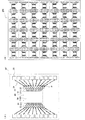
図1は、この発明の実施形態であるチップマウント用配線シートを示す図である。このチップマウント用配線シートは、複数の半導体チップをマウントして電気的に接続したのち、個々の半導体チップ毎に切り離してシートマウントチップを製造するためのシートであり、両面に破線パターンを形成可能なインターポーザ用の薄型樹脂で構成されている。 FIG. 1 is a view showing a chip mounting wiring sheet according to an embodiment of the present invention. This chip mounting wiring sheet is a sheet for mounting and electrically connecting a plurality of semiconductor chips, and then separating each semiconductor chip to manufacture a sheet mounting chip. A broken line pattern can be formed on both sides It is made of a thin resin for an interposer.
同図(B)は、シートマウントチップを切り離す前のチップマウント用配線シート200を示している。同図(A)はそのチップマウント配線シート200のうち1つの半導体チップに対応する単位区画20′を拡大図示したものである。1枚のシートマウント用配線チップ200には、この単位区画20′が複数形成されている(この実施形態では42区画設けられているが、400(=20×20)区画程度にしてもよい)。この単位区画20′のうち、中央部の配線シート部20が切り離されてシートマウントチップ60(図3参照)の配線シート部となる。配線シート部20の中央部には、半導体チップ50をマウントするためのチップマウントエリア100が設けられており、このチップマウントエリア100の内部にフリップチップ接続用の内部端子(パッド)21が形成されている。
FIG. 5B shows the chip
この図では、チップマウントエリア100に半導体チップ50がマウントされた状態を示しており、内部端子21に半導体チップ50の端子(バンプ)51が接続されている。
This figure shows a state in which the
また、配線シート部20の内部には、実装時にリードフレームや他の半導体チップなどの他の部品に接続される外部端子22が形成されている。この実施形態における外部端子22は、半導体チップ50がマウントされるチップマウントエリア100と同じ面で且つチップマウントエリア100の外側に形成されており、半導体チップ50側の面で他の部品とワイヤボンディング接続される。この外部端子22のピッチは、たとえば150μmピッチである。
In addition,
なお、半導体チップ50の端子51と内部端子101とをワイヤボンディングで接続する場合には、内部端子21をチップマウントエリア100の外側に設ける。また、他の部品との接続方式をバンプ接続にする場合、または、半導体チップ50と反対側の面で他の部品とワイヤボンディング接続する場合には、外部端子22は半導体チップ50(チップマウントエリア100)の面と反対側に形成する。
Note that, when the
また、単位区画20′の範囲内で配線シート部20の外側には、テスト用端子25が形成されている。テスト用端子は、テスト装置のテストピンが当接する端子であり、テストピンに合わせたピッチで形成されている。このピッチは、たとえば約0.5mmピッチであり、前記外部端子22のピッチよりも大きく形成されるのが一般的である。また、この実施形態では、テスト用端子25がチップマウントエリア100と同じ面に形成されているが、逆の面に形成するようにしてもよい。これは、テスト時のチップマウント用配線シート200の支持形態に応じて決定すればよい。
Further, a
これら、内部端子21、外部端子22およびテスト用端子25は、シート表面または内部に形成された内部配線23、24で互いに接続されている。
The
上記構成のチップマウント用配線シート200の各単位区画20′(チップマウントエリア100)に半導体チップ50をマウントして配線を行い、シート状態のまでテスト装置にセットして各種のテストを行う。
The
このテストは、上記チップマウント用配線シート200をテスト装置にセットして行う。テスト装置は、各テスト用端子25に対してテストピンを接続し、各半導体チップに対して各種の信頼性試験および動作試験を行う。この信頼性試験は、例えば高温バイアス試験(Burn-in) などである。そして、半導体チップ50(切断前のシートマウントチップ60)の良品/不良品を判別する。
This test is performed by setting the chip
なお、チップマウント用配線シート200は、フレキシブルなものである場合には、これをテスト装置にセットして各種試験を行うときには、シートを支持する支持材上にチップマウント用配線シート200を載置してテスト装置にセットするようすればよい。
When the chip mounting
テストののち、同図(A)に二点鎖線で示した配線シート部20の輪郭線に沿って切断することにより、シートマウントチップ60が完成する。このうち、不良品と判定されたチップを選別除外することにより、検査済チップKGDとしてのシートマウントチップを得ることができる。
After the test, the
シートマウントチップ60は、同図(A)に示すように、前記単位区画20′から、半導体チップ50がマウントされたチップマウントエリア100、内部端子21および外部端子22を含み、テスト用端子25を含まない形状に切り出される。したがって、シートマウントチップとして切り出された配線シート部20の端部領域Pには、外部端子22とテスト用端子25とを接続するための内部配線24の端部が残された状態になっている。
As shown in FIG. 2A, the
図2は上記テスト工程を含むシートマウントチップの製造工程を示すフローチャートである。チップマウント用配線シート200にマウントする半導体チップをウエハ状態でテストする(S11)。その後、ウエハの裏面を研磨して所定厚みまで薄くし(S12)、ウエハダイシングによって個別の半導体チップ50に分離する(S13)。これらの半導体チップのうち良品と見なされた半導体チップ50をチップマウント用配線シート200のチップマウントエリア100にマウントして必要な配線を施し(S14)、必要に応じて半導体チップ部分を樹脂封止する(S15)。この樹脂封止は、これ以後の工程におけるハンドリング性を高めるためのものであって、機械的強度は必要ない。
FIG. 2 is a flowchart showing a manufacturing process of the sheet mount chip including the test process. A semiconductor chip mounted on the chip mounting
その後、切断前のチップマウント用半導体シートのまま上述の信頼性試験および動作試験を行い、それぞれの半導体チップについて良否判定を行う(S16)。こののち、各配線シート部20の領域を切り離すことにより(S17)、シートマウントチップ60を製造する。
Thereafter, the above-described reliability test and operation test are performed with the chip mount semiconductor sheet before cutting, and pass / fail judgment is performed for each semiconductor chip (S16). Thereafter, the
一方、S21〜S27は、上記シートマウントチップ60を用いたSIPの製造工程を示すフローチャートであり、この工程によれば、図3に示すようなSIPが製造される。
On the other hand, S21 to S27 are flowcharts showing a SIP manufacturing process using the
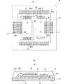
図3に示すSIPについて説明する。同図(A)はSIPの平面図、同図(B)はその主要部の断面図である。この図においてパッケージ基板10の上面には半導体チップ30がダイボンディングされており、その上に上述のシートマウントチップ60が実装されている。
The SIP shown in FIG. 3 will be described. 2A is a plan view of the SIP, and FIG. 2B is a cross-sectional view of the main part thereof. In this figure, the
シートマウントチップ60は、半導体チップ50を搭載しており、図1に示した実施形態とは異なり、半導体チップ50の端子51と内部端子21とがワイヤボンディングで接続され、外部端子22が配線シート部20の一辺のみに形成されているものである。このシートマウントチップ60はその下面(チップマウント用配線シート20の下面)を半導体チップ30に接着することによって実装されている。またこれとは別に、半導体チップ40を半導体チップ30の上に実装されている。
The
パッケージ基板10の上面には複数の端子11,11′が配列形成されている。またパッケージ基板10の下面には複数の半田ボール12が配列形成されている。このパッケージ基板10の上面の端子11,11′と下面の半田ボール12との間はパッケージ基板10内部の配線層を介して電気的に導通している。
A plurality of
半導体チップ30の上面の周囲に配列した端子とパッケージ基板10の上面に配列した端子11との間はワイヤW31によりワイヤボンディングされている。
Wire bonding is performed between the terminals arranged around the upper surface of the
なお、この図では、シートマウントチップ60の外部端子22は、配線シート部20の1辺に1列に配列されているが、外部端子の配列はSIPの構成に応じて最適に設計するようにすればよい。
In this figure, the
外部端子22とパッケージ基板10の端子11′との間はワイヤW21でワイヤボンディングされている。配線シート部20の内部配線を用いて端子の位置を変換することにより、半導体チップの外部接続用端子(パッド)の位置、ピッチ、信号配列などを変更することなく、既に存在する半導体チップをそのまま用いて電気的接続を容易に行えるようになる。
A wire W21 is used for wire bonding between the
なお、この例では、半導体チップ40は半導体チップ30とともにSIPとして用いるように既に設計されているのでサブ基板を用いていない。この半導体チップ40の上面の端子41と半導体チップ30の上面に形成した端子31との間はワイヤW43でワイヤボンディングしている。さらに、半導体チップ40の所定の端子41′とパッケージ基板上の端子11′との間はワイヤW41でワイヤボンディングしている。
In this example, since the
ここで、同図(A)は、パッケージ基板10上部の樹脂封止を行う前の状態を示しており、半導体チップ実装ののち、同図(B)に示すように、パッケージ基板10の上面には半導体チップ30,40、シートマウントチップ60およびそれらの間を接続するワイヤの全体を封止樹脂13で樹脂封止している。
Here, FIG. 4A shows a state before the resin sealing of the upper portion of the
ここで、半導体チップ30は他の半導体チップであり、そのサイズは例えば8.5mm×8.5mmである。半導体チップ40はその他の半導体チップである。サブ基板20上の半導体チップ50は例えば32M×32ビットのDRAMであり、そのサイズは例えば3.0mm×5.7mmである。SIPに実装される半導体チップのうち、DRAMが最も汎用品を使用する機会が多く、廉価且つ不良率の高い部品である。したがって、SIPのうちDRAMをシートマウントチップ化することにより、大幅なローコスト化、不良率の低減を実現することが可能になる。
Here, the
なお、シートマウントチップ60において、配線シート部20上の外部端子22をパッケージ基板10上の端子11′に沿うように配列形成したことにより、ワイヤW21のワイヤ長を短くすることが可能になっている。
In the
図2のフローチャートにもどって、まずパッケージ基板10にマウントする半導体チップのウエハ状態でのテストを行う(S21)。その後、ウエハ研磨、ウエハダイシングを行い(S22→S23)、各半導体チップ30をパッケージ基板10に搭載する(S24)。その後、上述のKGDであるシートマウントチップ60を搭載する(S25)。続いてパッケージ基板10の上部を樹脂封止し、個別のパッケージ基板に切り離す(S26)。そして各半導体装置について、上述のシートマウントチップ(チップマウント用配線シート)に対して行ったものと同様の各種信頼性試験および動作試験を行う(S27)。このようにして良品の半導体装置を得る。上記ステップS26を行う代わりに、パッケージ基板の切り離し前に複数の半導体装置について試験を行い、その後に樹脂封止し、パッケージ基板として切り離してもよい(S26′)。
Returning to the flowchart of FIG. 2, first, a test of a semiconductor chip mounted on the
図4は、チップマウント用配線シートの他の実施形態を示す図である。この実施形態では、このシートをテスト装置に接続するためのテスト用端子25をシートの端部に形成しており、各単位区画20′には、テスト用端子25が形成されていない。チップマウント用配線シート200には、複数の単位区画20′が縦横にアレイ状に配列されており、同図上辺に形成されているテスト用端子25に接続された縦方向の配線240が、縦方向の単位区画20′列を貫いて形成されている。各単位区画20′において、内部配線23がこの縦方向の配線240に接続され、これにより、各単位区画20′内の内部端子21がテスト用端子25に接続されることになる。
FIG. 4 is a view showing another embodiment of the chip mounting wiring sheet. In this embodiment, a
このような配線により、縦方向に配列された複数の単位区画20′の半導体チップ50には、共通の電源、バイアス電圧、テスト信号が供給される。このように、テスト用端子25を複数の半導体チップに対して共通化することにより、テスト用端子数を少なくして、多数の単位区画20′が形成されているチップマウント用配線シート200であっても、テスト用端子25を端部の1辺に集約することができる。
なお、この場合でも、テスト信号線に多重化したテスト信号を入力することにより、複数の半導体チップに対してそれぞれ独立したテストを行うことが可能である。
With such wiring, a common power supply, bias voltage, and test signal are supplied to the semiconductor chips 50 of the plurality of
Even in this case, it is possible to perform independent tests on a plurality of semiconductor chips by inputting multiplexed test signals to the test signal lines.
なお、上記実施形態では、シートマウントチップと他の部品との接続を、ワイヤボンディングやフリップチップ接続で行う旨説明したが、配線シート部をフレキシブルなシートで構成してその両端に端子を設け、この端子を接続すべき相手側の端子に圧着接続するようにしてもよい。 In the above embodiment, it has been described that the connection between the sheet mount chip and other components is performed by wire bonding or flip chip connection, but the wiring sheet portion is formed of a flexible sheet and terminals are provided at both ends thereof. You may make it crimp-connect to the terminal of the other party which should connect this terminal.
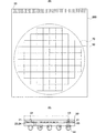
図1および図4の実施形態では、チップ単位にダイシングした半導体チップをチップマウント用配線シート200上にマウントするようにしているが、ダイシングする前のウェハ状態で半導体チップ50上にチップマウント用配線シート200を貼り付け、ウェハ状態のままで動作試験、信頼性試験を行うようにすることもできる。
In the embodiment shown in FIGS. 1 and 4, the semiconductor chip diced in units of chips is mounted on the chip mounting
図5は、このウェハ状態の半導体チップ50にチップマウント用配線シート200を貼り付けてテストしたのちダイシングして、シートマウントチップを製作する実施形態を説明する図である。同図(A)は、複数の半導体装置(半導体チップ)50が形成されたウェハ70の表面にチップマウント用配線シート200を貼り付けた状態を示す図である。同図(B)は、各半導体チップ毎にダイシングした状態を示す側断面図である。
FIG. 5 is a diagram for explaining an embodiment in which a chip
チップマウント用配線シート200は、2層の配線層を有しており、表面には、ウェハ70の表面に形成されている半導体チップ50のパッドに当接する内部端子21が形成されている。そして、前記2層の配線層を介してシート裏面の外部電極22である実装用バンプに接続されている。
The chip-
また、方形のチップマウント用配線シート20の1辺(同図における上辺)には、テスト用端子25が形成されている。各半導体チップ50の端子51は、前記2層の配線層を介してテスト用端子25に接続されている。
A
上記構成のシートマウント用配線シート200を、前工程が終了したウェハ70に位置合わせして貼り付け、半導体チップ50の端子51と内部端子21とを接合する。
The sheet mounting
この状態で、テスト装置にセットしてテスト用端子25をテスト装置の電極に接続し、Burn−inを含む各種のテストを行う。
In this state, the
こののち、このウェハをダイサーにセットしてダイシングを行い、G/W工程で良品とされ、上記テスト装置によるテストでも良品と判定されたチップのみを選別してKGDのシートマウントチップとする。 After that, the wafer is set on a dicer and diced, and only chips that are determined to be non-defective in the G / W process and determined to be non-defective in the test by the test apparatus are selected as KGD sheet mount chips.
なお、このシートマウント用配線シートにおいても、テスト用端子25を複数の半導体チップ50で共有するようにすればよい。
In this sheet mounting wiring sheet, the
9−リードフレーム
10−パッケージ基板
11−端子
12−半田ボール
13−封止樹脂
20−配線シート部
20′−単位区画
21−内部端子、
22−外部端子
23,24−内部配線
25−テスト用端子
30,40,50−半導体チップ
31,41,51−端子
60−シートマウントチップ
70−(半導体チップ50が形成された)ウェハ
100−チップマウントエリア
200−チップマウント用配線シート
W−ワイヤ
9-lead frame 10-package substrate 11-terminal 12-solder ball 13-sealing resin 20-wiring sheet portion 20'-unit section 21-internal terminal,
22-
Claims (10)
チップマウント部にマウントされた半導体チップに接続される内部端子と、
実装時に他の部品に接続される外部端子と、
試験時に試験装置の端子が接続されるテスト用端子と、
前記内部端子と前記外部端子およびテスト用端子とを電気的に接続する内部配線と、
を各半導体チップ毎に備えたことを特徴とするチップマウント用配線シート。 A wiring sheet for mounting a plurality of semiconductor chips,
Internal terminals connected to the semiconductor chip mounted on the chip mount portion;
External terminals connected to other components during mounting,
A test terminal to which the terminal of the test apparatus is connected during the test;
An internal wiring for electrically connecting the internal terminal, the external terminal and the test terminal;
Is provided for each semiconductor chip.
テスト用端子に試験装置の端子を接続して各半導体チップの試験を行う手順、
各半導体チップ毎に、チップマウント部、内部端子および外部端子を含み、テスト用端子を含まない形状に切り抜く手順、
を有することを特徴とするシートマウントチップの製造方法。 A procedure for mounting a semiconductor chip on the chip mounting wiring sheet according to any one of claims 1 to 4,
A procedure for testing each semiconductor chip by connecting a test device terminal to a test terminal,
For each semiconductor chip, including a chip mount part, internal terminals and external terminals, and a procedure for cutting out into a shape not including test terminals,
A method for manufacturing a sheet mount chip, comprising:
各半導体チップのパッドに対向して電気的に接続される内部端子と、
貼付面の裏面に形成され、実装時に他の部品に接続される外部端子と、
前記ウェハの貼り付け範囲外または貼付面の裏面に形成され、試験時に試験装置の端子が接続されるテスト用端子と、
前記内部端子と前記外部端子およびテスト用端子とを電気的に接続する内部配線と、
を備えたことを特徴とするチップマウント用配線シート。 A wiring sheet attached to a wafer on which a plurality of semiconductor chips are formed,
Internal terminals electrically connected to the pads of each semiconductor chip;
An external terminal formed on the back side of the affixing surface and connected to other components at the time of mounting;
A test terminal to which a terminal of a test apparatus is connected at the time of a test, which is formed on the back side of the affixing surface of the wafer or on the back side of the affixing surface;
An internal wiring for electrically connecting the internal terminal, the external terminal and the test terminal;
A chip mounting wiring sheet comprising:
テスト用端子に試験装置の端子を接続して各半導体チップの試験を行う手順、
前記ウェハおよびチップマウント用配線シートを各半導体チップ毎にカットする手順、
を有することを特徴とするシートマウントチップの製造方法。 A procedure for attaching a wafer on which a semiconductor chip is formed on the chip mounting wiring sheet according to claim 7 or 8,
A procedure for testing each semiconductor chip by connecting a test device terminal to a test terminal,
A procedure for cutting the wafer and chip mounting wiring sheet for each semiconductor chip;
A method for manufacturing a sheet mount chip, comprising:
Priority Applications (2)
| Application Number | Priority Date | Filing Date | Title |
|---|---|---|---|
| JP2003364389A JP2007019049A (en) | 2003-10-24 | 2003-10-24 | Chip-mount wiring sheet, sheet-mounted chip, and manufacturing method thereof |
| PCT/JP2004/002342 WO2005041296A1 (en) | 2003-10-24 | 2004-02-27 | Chip-mount wiring sheet, sheet-mounted chip, and sheet-mounted chip manufacturing method |
Applications Claiming Priority (1)
| Application Number | Priority Date | Filing Date | Title |
|---|---|---|---|
| JP2003364389A JP2007019049A (en) | 2003-10-24 | 2003-10-24 | Chip-mount wiring sheet, sheet-mounted chip, and manufacturing method thereof |
Publications (1)
| Publication Number | Publication Date |
|---|---|
| JP2007019049A true JP2007019049A (en) | 2007-01-25 |
Family
ID=34510107
Family Applications (1)
| Application Number | Title | Priority Date | Filing Date |
|---|---|---|---|
| JP2003364389A Pending JP2007019049A (en) | 2003-10-24 | 2003-10-24 | Chip-mount wiring sheet, sheet-mounted chip, and manufacturing method thereof |
Country Status (2)
| Country | Link |
|---|---|
| JP (1) | JP2007019049A (en) |
| WO (1) | WO2005041296A1 (en) |
Family Cites Families (3)
| Publication number | Priority date | Publication date | Assignee | Title |
|---|---|---|---|---|
| US5367763A (en) * | 1993-09-30 | 1994-11-29 | Atmel Corporation | TAB testing of area array interconnected chips |
| JP3527015B2 (en) * | 1996-06-10 | 2004-05-17 | 株式会社ルネサステクノロジ | Semiconductor device and manufacturing method thereof |
| JP2001176940A (en) * | 1999-12-20 | 2001-06-29 | Sharp Corp | Method for manufacturing semiconductor module |
-
2003
- 2003-10-24 JP JP2003364389A patent/JP2007019049A/en active Pending
-
2004
- 2004-02-27 WO PCT/JP2004/002342 patent/WO2005041296A1/en not_active Application Discontinuation
Also Published As
| Publication number | Publication date |
|---|---|
| WO2005041296A1 (en) | 2005-05-06 |
Similar Documents
| Publication | Publication Date | Title |
|---|---|---|
| US9653427B2 (en) | Integrated circuit package with probe pad structure | |
| US8994163B2 (en) | Semiconductor assemblies, stacked semiconductor devices, and methods of manufacturing semiconductor assemblies and stacked semiconductor devices | |
| US9129914B2 (en) | Electronic device, test board, and semiconductor device manufacturing method | |
| US7723835B2 (en) | Semiconductor device package structure | |
| US8076179B2 (en) | Fabrication method for integrated circuit chip component, multi-chip module, and their integration structure | |
| CN108140615B (en) | Guard ring design to enable in-line testing of silicon bridges for semiconductor packages | |
| JP2010206007A (en) | Semiconductor device and method of manufacturing the same | |
| KR20030014637A (en) | Semiconductor wafer, semiconductor device, and method for manufacturing the same | |
| EP2645417A1 (en) | Semiconductor module | |
| TWI474444B (en) | Package method of thin multi-layer substrate | |
| TW201328456A (en) | Package method of thin multi-layer substrate | |
| TWI440412B (en) | Package method of thin multi-layer substrate | |
| JP4388926B2 (en) | Package structure of semiconductor device | |
| JP3842272B2 (en) | Interposer, semiconductor chip mount sub-board and semiconductor package | |
| WO2019011457A1 (en) | Non-destructive testing of integrated circuit chips | |
| US9263379B2 (en) | IC package with metal interconnect structure implemented between metal layers of die and interposer | |
| JP2007019049A (en) | Chip-mount wiring sheet, sheet-mounted chip, and manufacturing method thereof | |
| US7420206B2 (en) | Interposer, semiconductor chip mounted sub-board, and semiconductor package | |
| JP2007142128A (en) | Semiconductor device and its production process | |
| JP4303772B2 (en) | Semiconductor package | |
| JP2005158768A (en) | Semiconductor device and its manufacturing method | |
| JP4388989B2 (en) | Semiconductor chip mount sealing sub-board | |
| JP2008300604A (en) | Manufacturing method of semiconductor device | |
| WO1999026289A1 (en) | Semiconductor device and method for manufacturing the same | |
| JP2005353687A (en) | Substrate for semiconductor device, and method of manufacturing semiconductor device |
Legal Events
| Date | Code | Title | Description |
|---|---|---|---|
| A521 | Written amendment |
Free format text: JAPANESE INTERMEDIATE CODE: A523 Effective date: 20061023 |
|
| A621 | Written request for application examination |
Free format text: JAPANESE INTERMEDIATE CODE: A621 Effective date: 20061023 |
|
| A131 | Notification of reasons for refusal |
Free format text: JAPANESE INTERMEDIATE CODE: A131 Effective date: 20090421 |
|
| A521 | Written amendment |
Free format text: JAPANESE INTERMEDIATE CODE: A523 Effective date: 20090622 |
|
| A131 | Notification of reasons for refusal |
Free format text: JAPANESE INTERMEDIATE CODE: A131 Effective date: 20090714 |
|
| A02 | Decision of refusal |
Free format text: JAPANESE INTERMEDIATE CODE: A02 Effective date: 20100119 |