JP2007000915A - Soldering method and soldering device - Google Patents
Soldering method and soldering device Download PDFInfo
- Publication number
- JP2007000915A JP2007000915A JP2005186111A JP2005186111A JP2007000915A JP 2007000915 A JP2007000915 A JP 2007000915A JP 2005186111 A JP2005186111 A JP 2005186111A JP 2005186111 A JP2005186111 A JP 2005186111A JP 2007000915 A JP2007000915 A JP 2007000915A
- Authority
- JP
- Japan
- Prior art keywords
- pressure
- chamber
- solder
- soldering
- heating
- Prior art date
- Legal status (The legal status is an assumption and is not a legal conclusion. Google has not performed a legal analysis and makes no representation as to the accuracy of the status listed.)
- Pending
Links
Images


Classifications
-
- H—ELECTRICITY
- H01—ELECTRIC ELEMENTS
- H01L—SEMICONDUCTOR DEVICES NOT COVERED BY CLASS H10
- H01L24/00—Arrangements for connecting or disconnecting semiconductor or solid-state bodies; Methods or apparatus related thereto
- H01L24/74—Apparatus for manufacturing arrangements for connecting or disconnecting semiconductor or solid-state bodies
- H01L24/75—Apparatus for connecting with bump connectors or layer connectors
-
- H—ELECTRICITY
- H01—ELECTRIC ELEMENTS
- H01L—SEMICONDUCTOR DEVICES NOT COVERED BY CLASS H10
- H01L24/00—Arrangements for connecting or disconnecting semiconductor or solid-state bodies; Methods or apparatus related thereto
- H01L24/80—Methods for connecting semiconductor or other solid state bodies using means for bonding being attached to, or being formed on, the surface to be connected
- H01L24/83—Methods for connecting semiconductor or other solid state bodies using means for bonding being attached to, or being formed on, the surface to be connected using a layer connector
-
- H—ELECTRICITY
- H01—ELECTRIC ELEMENTS
- H01L—SEMICONDUCTOR DEVICES NOT COVERED BY CLASS H10
- H01L2224/00—Indexing scheme for arrangements for connecting or disconnecting semiconductor or solid-state bodies and methods related thereto as covered by H01L24/00
- H01L2224/80—Methods for connecting semiconductor or other solid state bodies using means for bonding being attached to, or being formed on, the surface to be connected
- H01L2224/83—Methods for connecting semiconductor or other solid state bodies using means for bonding being attached to, or being formed on, the surface to be connected using a layer connector
-
- H—ELECTRICITY
- H01—ELECTRIC ELEMENTS
- H01L—SEMICONDUCTOR DEVICES NOT COVERED BY CLASS H10
- H01L2924/00—Indexing scheme for arrangements or methods for connecting or disconnecting semiconductor or solid-state bodies as covered by H01L24/00
- H01L2924/15—Details of package parts other than the semiconductor or other solid state devices to be connected
- H01L2924/151—Die mounting substrate
- H01L2924/156—Material
- H01L2924/15786—Material with a principal constituent of the material being a non metallic, non metalloid inorganic material
- H01L2924/15787—Ceramics, e.g. crystalline carbides, nitrides or oxides
Landscapes
- Engineering & Computer Science (AREA)
- Computer Hardware Design (AREA)
- Microelectronics & Electronic Packaging (AREA)
- Power Engineering (AREA)
- Manufacturing & Machinery (AREA)
- Die Bonding (AREA)
Abstract
Description
本発明は、半田付け方法及び半田付け装置に関し、特に、半田付け時に半田内に形成される空隙を減少させるものに関する。 The present invention relates to a soldering method and a soldering apparatus, and more particularly, to a device that reduces voids formed in solder during soldering.
複数、例えば2つの接合対象物を半田接合することがある。例えば半導体装置のような電気素子と、この電気素子に対する放熱板とを、電気素子からの放熱を目的として、半田接合することがある。このような半田接合は、例えば放熱板の接合面に半田を配置し、その半田の上に電気素子を配置し、加熱することによって半田を溶融させ、その後に冷却することによって溶融された半田を凝固させて、電気素子と放熱板とを半田接合する。しかし、このような半田接合では、凝固後の半田内部に多数の空隙が存在することがある。この空隙が熱伝導率を低下させる。接合後の半田内の空隙を減少させるための技術が、例えば特許文献1に開示されている。
A plurality of, for example, two objects to be joined may be soldered. For example, an electric element such as a semiconductor device and a heat dissipation plate for the electric element may be soldered for the purpose of heat dissipation from the electric element. Such solder bonding is performed by, for example, placing solder on the joining surface of the heat sink, placing an electrical element on the solder, melting the solder by heating, and then cooling the molten solder by cooling. It solidifies and solders an electric element and a heat sink. However, in such a solder joint, there may be a large number of voids inside the solder after solidification. This void reduces the thermal conductivity. For example,
特許文献1の技術では、内部の温度及び圧力を調整可能な半田付け装置内に、接合対象物をそれらの間に半田を挿入した状態で配置する。半田付け装置内を真空に近い低圧で、半田付け装置内の温度を上昇させることによって、半田を溶融し、その後に半田付け装置内の温度を低下させて、半田付けする。半田の溶融後に、半田付け装置内の圧力を大気圧まで上昇させて、半田内に形成されている空隙(ボイド)を押しつぶす。なお、半導体素子やICチップと基板上の所定の配線パターンとを半田接合する場合にも同様に行われる。
In the technique of
上記文献の技術では、半田が溶融した状態において、半田付け装置内の圧力を上昇させることによって、ボイドをつぶそうとしている。そのため、半田の溶融を低圧の状態で行っている。しかし、真空に近い圧力において、半田を加熱溶融すると、半田の還元が不十分で、半田の濡れ不良が発生する。この点を改善するため、上記の文献1では、真空に近い圧力において、水素ラジカルの雰囲気として、半田の還元を行っている。
In the technique of the above document, the void is crushed by increasing the pressure in the soldering apparatus in a state where the solder is melted. Therefore, the solder is melted at a low pressure. However, when the solder is heated and melted at a pressure close to a vacuum, the solder is not sufficiently reduced, resulting in poor solder wetting. In order to improve this point, in
本発明は、水素ラジカル雰囲気を使用せずに、半田の還元を行うことができ、かつボイドを溶融半田中から追い出すことができる半田付け方法及び半田付け装置を提供することを目的とする。 It is an object of the present invention to provide a soldering method and a soldering apparatus that can reduce solder without using a hydrogen radical atmosphere and can expel voids from molten solder.
本発明による半田付け方法では、溶融過程として、圧力がほぼ大気圧の還元雰囲気または不活性雰囲気中において、半田とこの半田によって半田付けされる被半田付け体とを備える半田付け処理物を加熱して、前記半田を溶融させることが行われる。前記半田の溶融状態において、圧力変化過程として、前記圧力を前記ほぼ大気圧から減圧し、その後に前記ほぼ大気圧の還元雰囲気または不活性雰囲気に戻すことが行われる。この圧力変化過程の後に、前記ほぼ大気圧の還元雰囲気または不活性雰囲気において冷却過程として、前記半田付け処理物を冷却することが行われる。 In the soldering method according to the present invention, as a melting process, in a reducing atmosphere or an inert atmosphere at a pressure of approximately atmospheric pressure, a soldering object including a solder and a soldered body to be soldered by the solder is heated. Then, the solder is melted. In the molten state of the solder, as a pressure changing process, the pressure is reduced from the substantially atmospheric pressure, and then returned to the reducing atmosphere or inert atmosphere at the substantially atmospheric pressure. After the pressure change process, the soldered product is cooled as a cooling process in the reducing atmosphere or inert atmosphere at approximately atmospheric pressure.
この半田付け方法では、半田が溶融した後に、圧力が大気圧から減圧されるので、半田の溶融中にその内部に発生したボイドが膨張し、溶融中の半田から抜ける。これによって、半田中から大部分のボイドが抜けるが、もし、わずかなボイドが半田中に残存したとしても、圧力が再び大気圧に近い状態に戻されるので、残存したボイドが圧縮され、固化した後に残ったボイドは、ごくわずかな体積しか持たない。しかも、半田の溶融は、ほぼ大気圧の還元雰囲気または不活性雰囲気で行われているので、半田の濡れも充分である。 In this soldering method, since the pressure is reduced from the atmospheric pressure after the solder is melted, voids generated inside the solder expand during the melting of the solder and come out of the molten solder. As a result, most of the voids are removed from the solder, but even if a small amount of voids remain in the solder, the pressure is returned to a state close to atmospheric pressure, so the remaining voids are compressed and solidified. The remaining voids have a negligible volume. In addition, since the solder is melted in a reducing atmosphere or an inert atmosphere at almost atmospheric pressure, the solder is sufficiently wetted.
この半田付け方法では、前記圧力変化過程を複数回にわたって繰り返すことができる。このように圧力変化過程を複数回、繰り返すことによって、確実に半田中に残存するボイドを減少させることができる。 In this soldering method, the pressure change process can be repeated a plurality of times. Thus, by repeating the pressure changing process a plurality of times, it is possible to reliably reduce the voids remaining in the solder.
本発明の一態様による半田付け装置は、半田付け処理物が、順に移動可能な加熱チャンバと冷却チャンバとを備えている。加熱チャンバと冷却チャンバとは、仕切り手段が設けられ、一方の雰囲気が他方の雰囲気に影響されないようにすることが望ましい。半田付け処理物は、半田と、この半田によって半田付けされる被半田付け体とを、備えている。この半田付け処理物は、加熱チャンバから冷却チャンバに移動する。前記加熱チャンバは、前記半田が溶融する温度に加熱する加熱手段を、備えている。この加熱手段による加熱状態において圧力調整手段が前記加熱チャンバの圧力を変化させる。すなわち、前記加熱チャンバを、その圧力がほぼ大気圧の還元雰囲気または不活性雰囲気とし、その後に前記加熱チャンバを減圧し、再びほぼ大気圧の還元雰囲気または不活性雰囲気とする。前記冷却チャンバは、前記半田付け処理物を冷却する冷却手段を有している。 A soldering apparatus according to an aspect of the present invention includes a heating chamber and a cooling chamber in which a soldering object can move in order. It is desirable that the heating chamber and the cooling chamber are provided with partition means so that one atmosphere is not affected by the other atmosphere. The soldered product includes solder and a body to be soldered that is soldered by the solder. This soldering process moves from the heating chamber to the cooling chamber. The heating chamber includes heating means for heating to a temperature at which the solder melts. The pressure adjusting means changes the pressure of the heating chamber in the heating state by the heating means. That is, the heating chamber is set to a reducing atmosphere or an inert atmosphere having a pressure of approximately atmospheric pressure, and then the heating chamber is depressurized to be set to a reducing atmosphere or an inert atmosphere of approximately atmospheric pressure again. The cooling chamber has a cooling means for cooling the soldering processed product.
このように構成された半田付け装置では、加熱チャンバに半田付け処理物が存在する状態において、上記の半田付け方法について説明したのと同様にして、半田付け処理物の加熱、圧力変化に伴って、ボイドの溶融半田からの放出が行われ、冷却チャンバにおいて半田の固化が行われる。 In the soldering apparatus configured as described above, in the state where the soldering process object exists in the heating chamber, in the same manner as the above-described soldering method, the heating process and the pressure change of the soldering process object are performed. The voids are released from the molten solder, and the solder is solidified in the cooling chamber.
この半田付け装置において、前記加熱チャンバの前に、圧力がほぼ大気圧の還元雰囲気または不活性雰囲気の状態と、大気状態とに、切換可能な前側ロードロックチャンバを、前記冷却チャンバの後ろに、圧力がほぼ大気圧の還元性雰囲気または不活性雰囲気の状態と、大気状態とに、切換可能な後ろ側ロードロックチャンバをそれぞれ設けることが望ましい。 In this soldering apparatus, before the heating chamber, a front load lock chamber that can be switched between a reducing atmosphere or an inert atmosphere having a pressure of approximately atmospheric pressure and an atmospheric state is provided behind the cooling chamber. It is desirable to provide a rear load lock chamber that can be switched between a reducing atmosphere or an inert atmosphere at a pressure of approximately atmospheric pressure and an atmospheric state.
このように構成することによって、或る半田付け処理物を加熱チャンバ及び冷却チャンバによって半田付けしている間に、別の半田付け処理物を前側チャンバにおいて圧力がほぼ大気圧の還元雰囲気または不活性雰囲気中において置けるので、或る半田付け処理物の処理が終了すると、別の半田付け処理物を前側チャンバから加熱チャンバに送ることによって、直ちに別の半田付け処理物の半田付け処理を開始することができる。すなわち、加熱チャンバにおいて、その内部を排気し、その後に、圧力がほぼ大気圧の還元雰囲気または不活性雰囲気に置換する必要がなく、半田付け処理を高速化できる。同様に、冷却チャンバで冷却された半田付け処理物は、後側ロードロックチャンバに送られた後に、圧力がほぼ大気圧の還元性ガスまたは不活性ガスを排気し、その後に大気状態に戻すことができる。従って、冷却チャンバにおいて、圧力がほぼ大気圧の還元雰囲気ガスまたは不活性雰囲気ガスを排気し、その後に大気状態に戻す作業が不要で、半田付け処理を高速化できる。 With this configuration, while one soldering process is being soldered by the heating chamber and the cooling chamber, another soldering process is performed in a reducing atmosphere or an inert atmosphere having a pressure of approximately atmospheric pressure in the front chamber. Since it can be placed in the atmosphere, when the processing of one soldering process is completed, another soldering process is sent from the front chamber to the heating chamber to immediately start another soldering process. Can do. That is, it is not necessary to evacuate the inside of the heating chamber and then replace it with a reducing atmosphere or an inert atmosphere whose pressure is almost atmospheric pressure, and the soldering process can be speeded up. Similarly, after the soldered product cooled in the cooling chamber is sent to the rear load lock chamber, the reducing or inert gas having a pressure of approximately atmospheric pressure is exhausted, and then returned to the atmospheric state. Can do. Accordingly, it is not necessary to exhaust the reducing atmosphere gas or the inert atmosphere gas having a pressure of approximately atmospheric pressure in the cooling chamber and then return to the atmospheric state, and the soldering process can be speeded up.
本発明の別の態様の半田付け装置は、圧力がほぼ大気圧である還元雰囲気または不活性雰囲気のチャンバを有している。このチャンバ内に、半田とこの半田によって半田付けされる被半田付け体とを備える半田付け処理物が搬送される搬送経路が設けられている。 前記搬送経路の中途に加熱手段が設けられ、前記被半田付け処理物を前記半田の溶融温度に加熱する。この加熱手段による加熱状態において、前記半田付け処理物の周囲の圧力を減少させ、その後に前記チャンバ内の圧力に戻す圧力変更手段が設けられている。この圧力変更手段としては、排気手段に接続された別のチャンバを上記チャンバ内の加熱手段中の半田付け処理物を内部に収容可能に設け、この別のチャンバ内に半田付け処理物が収容された状態で、別のチャンバ内を排気するものを使用することができる。前記加熱手段よりも後方の搬送経路において、前記半田付け処理物を冷却する冷却手段が設けられている。 The soldering apparatus according to another aspect of the present invention includes a chamber in a reducing atmosphere or an inert atmosphere whose pressure is approximately atmospheric pressure. In the chamber, there is provided a transport path for transporting a soldering process object including solder and a soldered body to be soldered by the solder. A heating means is provided in the middle of the conveyance path, and heats the soldering object to the melting temperature of the solder. In the heating state by the heating means, a pressure changing means is provided for reducing the pressure around the soldering object and then returning it to the pressure in the chamber. As this pressure changing means, another chamber connected to the exhaust means is provided so that the soldering processed product in the heating means in the chamber can be accommodated therein, and the soldering processed product is accommodated in this separate chamber. In such a state, an apparatus for exhausting the inside of another chamber can be used. Cooling means for cooling the soldered product is provided in the transport path behind the heating means.
この半田付け装置においても、上記の半田付け方法について説明したのと同様にして、半田付け処理物の加熱、圧力変化に伴うボイドの溶融半田からの放出、半田の固化が行われる。しかも、この半田付け処理は、1つのチャンバ内において行われる。 In this soldering apparatus, similarly to the above-described soldering method, heating of the soldered material, release of voids from the molten solder accompanying pressure change, and solidification of the solder are performed. Moreover, this soldering process is performed in one chamber.
この半田付け装置において、前記チャンバの前後に、圧力がほぼ大気圧の不活性雰囲気の状態と、大気状態とに、切換可能なロードロックチャンバをそれぞれ設けることもできる。 In this soldering apparatus, a load-lock chamber that can be switched between an inert atmosphere state at a pressure of approximately atmospheric pressure and an atmospheric state can be provided before and after the chamber.
このように構成することによって、或る半田付け処理物をチャンバによって半田付けしている間に、別の半田付け処理物をチャンバの前側にある別のロードロックチャンバにおいて圧力がほぼ大気圧の還元雰囲気または不活性雰囲気中において置けるので、或る半田付け処理物の処理が終了すると、別の半田付け処理物を前側の別のロードロックチャンバからチャンバに送ることによって、直ちに別の半田付け処理物の半田付け処理を開始することができる。すなわち、チャンバにおいて、その内部を排気し、その後に、圧力がほぼ大気圧の還元雰囲気または不活性雰囲気に置換する必要がなく、半田付け処理を高速化できる。同様に、チャンバで冷却された半田付け処理物は、後側の別のロードロックチャンバに送られた後に、圧力がほぼ大気圧の還元性ガスまたは不活性ガスを排気し、その後に大気状態に戻すことができる。従って、チャンバにおいて、圧力がほぼ大気圧の還元性ガスまたは不活性ガスを排気し、その後に大気状態に戻す作業が不要で、半田付け処理を高速化できる。 With this configuration, while one soldering process is being soldered by the chamber, another soldering process is reduced to approximately atmospheric pressure in another loadlock chamber on the front side of the chamber. Since it can be placed in an atmosphere or an inert atmosphere, when the processing of a certain soldering process is completed, another soldering process is immediately performed by sending another soldering process from another load lock chamber to the chamber. The soldering process can be started. That is, it is not necessary to evacuate the inside of the chamber and then replace it with a reducing atmosphere or an inert atmosphere whose pressure is almost atmospheric pressure, and the soldering process can be speeded up. Similarly, after the soldered workpiece cooled in the chamber is sent to another load lock chamber on the rear side, the reducing or inert gas having a pressure of about atmospheric pressure is exhausted, and then the atmosphere is brought to an atmospheric state. Can be returned. Accordingly, it is not necessary to exhaust the reducing gas or the inert gas having a pressure of approximately atmospheric pressure in the chamber and then return to the atmospheric state, and the soldering process can be speeded up.
以上のように、本発明によれば、半田の濡れを良好にすることができる上に、ボイドを溶融半田中から確実に追い出すことができる。 As described above, according to the present invention, the wetness of the solder can be improved, and the void can be surely expelled from the molten solder.
本発明の第1の実施形態の半田付け装置は、半田付け処理物1として、例えば図3(a)に示すように、セラミック基板2とICチップ4とを使用し、セラミック基板2上の所定の配線パターン上に半田6を挟んでICチップ4を配置してある。この半田付け処理物1が、半田付け装置内を通過していく間に、半田6の溶融及び固化が行われ、セラミック基板2とICチップ4とが半田付けされる。セラミック基板2とICチップ4とが、被半田付け体である。
The soldering apparatus according to the first embodiment of the present invention uses a
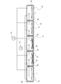
この半田付け装置は、図2に示すように、前側ロードロックチャンバ10、予熱チャンバ12、加熱チャンバ14、冷却チャンバ16及び後ろ側ロードロックチャンバ18を有している。これらは、上記の順に配置され、それぞれの間にはゲート20が配置されている。図示していないが、ロードロックチャンバ10、予熱チャンバ12、加熱チャンバ14、冷却チャンバ16及びロードロックチャンバ18間を、半田付け処理物1を搬送するための搬送手段が設けられ、図2に矢印で示す搬送経路に沿って半田付け処理物1が搬送される。
As shown in FIG. 2, the soldering apparatus includes a front
ロードロックチャンバ10には、外部と内部とを遮断するゲート22も設けられており、予熱チャンバ12との境界のゲート20を閉じた状態で、半田付け処理物1が導入され、真空ポンプ24によって真空、例えば約133Pa以下まで排気され、ガス供給源26から不活性ガス、例えば窒素ガスまたは還元性ガス、例えば水素ガスが供給され、ロードロックチャンバ10の圧力は、ほぼ大気圧とされる。なお、ロードロックチャンバ10内の温度は室温である。
The
予熱チャンバ12内に半田付け処理物1が存在しない状態において、予熱チャンバ12とロードロックチャンバ10との間のゲート20が開かれ、半田付け処理物1が予熱チャンバ12に搬送される。その後、このゲート20は閉じられる。予熱チャンバ12内は、予め真空ポンプ24及びガス供給源26によって、窒素ガスまたは水素ガスが充填され、その圧力はほぼ大気圧とされている。予熱チャンバ12内には、予熱手段、例えば予熱ヒータ28が設置されており、これによって、予熱チャンバ12内の温度は、半田6の溶融温度よりわずかに低い温度とされている。従って、室温であるロードロックチャンバ10から搬送された半田付け処理物1の温度は、半田6の溶融温度付近まで、予熱チャンバ12によって上昇させられる。
In a state where the
予熱チャンバ12によって半田付け処理物1の温度が上昇させられ、かつ加熱チャンバ14内に半田付け処理物1が存在しない状態において、予熱チャンバ12と加熱チャンバ14との間のゲート20が開かれ、半田付け処理物1が加熱チャンバ14に搬送される。その後、ゲート20は閉じられる。加熱チャンバ14は、予め真空ポンプ24及びガス供給源26によって、窒素ガスまたは水素ガスが充填され、その圧力はほぼ大気圧とされている。さらに、加熱チャンバ14内には、加熱手段、例えば加熱ヒータ30が設置されており、これによって、加熱チャンバ14内の温度は、半田6の溶融温度以上の温度とされている。
In the state where the temperature of the
窒素ガス雰囲気または水素ガス雰囲気中において、半田6は溶融されるので、半田6の濡れが充分に確保される。このように半田6が溶融した状態において、真空ポンプ24を作動させて、加熱チャンバ14内の圧力を真空状態、例えば約133Pa以下の真空状態にする。即ち、加熱チャンバ14が大きく減圧される。図3(a)に示すように、溶融された半田6内に形成されていたボイド32は、減圧によって同図(b)に示すように膨張し、ICチップ4を押し上げて、半田6から放出される。なお、ほぼ大気圧から約133Pa以下の真空状態に減圧することによって、ボイド32の体積は、約700乃至800倍に膨張する。
Since the
加熱チャンバ14内の圧力がほぼ真空状態とされると、ガス供給源26から再び窒素ガスまたは水素ガスが供給され、加熱チャンバ14の圧力は再びほぼ大気圧とされる。これによって、溶融された半田6内に残存していたボイド32は無視することができる程度の容積まで大きく圧縮される。
When the pressure in the
このように圧力を、ほぼ大気圧から真空とする過程が複数回、例えば2回繰り返される。これによって、溶融半田中のボイドは、膨張、圧縮を複数回にわたって繰り返し、その結果、図3(c)に示すように、溶融された半田6中には、ボイド32は存在しなくなる。即ち、ボイド32が溶融された半田6中から抜かれる。
In this way, the process of changing the pressure from approximately atmospheric pressure to vacuum is repeated a plurality of times, for example, twice. As a result, the voids in the molten solder are repeatedly expanded and compressed a plurality of times. As a result, as shown in FIG. 3C, the void 32 does not exist in the
上記のようにして、ボイド32を抜いた後であって、冷却チャンバ16内に半田付け処理物1が存在しない状態において、冷却チャンバ16と加熱チャンバ14との間のゲート20が開かれて、半田付け処理物1が冷却チャンバ16に搬送される。その後、ゲート20は閉じられる。冷却チャンバ16内には、水素ガス、または窒素ガスが充填され、その圧力は、ほぼ大気圧とされている。この冷却チャンバ16内には、冷却手段、例えば冷却盤34が配置されている。この冷却盤34は、半田付け処理物1に接触して、半田付け処理物1を例えば常温まで冷却し、溶融している半田を固化させる。冷却盤34としては、例えば水冷式のものを使用することができる。
As described above, after the void 32 is removed and the
このように冷却が終了した後で、ロードロックチャンバ18内に半田付け処理物1が存在しない状態において、冷却チャンバ16と冷却チャンバ14との間のゲート20が開かれて、半田付け処理物1がロードロックチャンバ18に搬送される。その後、ゲート20が閉じられる。このとき、ロードロックチャンバ18の外界との間のゲート36も閉じられている。この状態において、ロードロックチャンバ18内は、窒素ガスまたは水素ガスが充填され、その圧力はほぼ大気圧とされている。ここで、ゲート36を開いて、半田付けの終了した半田付け処理物1が取り出される。しかし、ロードロックチャンバ18内に水素ガスが充填されている場合には、ゲート36を開く前に、一旦真空排気した後、不活性ガスを導入し、ロードロックチャンバ18の圧力をほぼ大気圧とする動作が追加される。
After the cooling is completed in this way, the
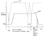
半田付け処理物1が半田付け装置において受ける圧力変化と温度変化を、図1に示す。図1から明らかなように、半田付け処理物1は、窒素ガスのような不活性ガス雰囲気または水素ガスのような還元性ガス雰囲気中において、半田6の溶融温度以上の温度に加熱されて、溶融される。半田6の溶融後に、水素ガスまたは窒素ガスが排気されて、真空状態、たとえば約133Pa以下とされる。これによって、溶融半田6中のボイドを膨張させて、ボイドを溶融半田6中から抜き、その後に圧力がほぼ大気圧となるまで水素ガスまたは窒素ガスが導入され、溶融半田6中に残ったボイドがある場合、これを無視することができる程度の容積まで大きく圧縮する。再び真空状態とされ、再度大気圧とされる。2回にわたって、大気圧から真空に圧力変化させることを繰り返し、確実にボイドを溶融半田6中から除いた後、還元雰囲気または不活性雰囲気中で冷却される。
FIG. 1 shows changes in pressure and temperature that the
この実施の形態では、不活性ガスまたは還元性ガス雰囲気中で半田6を溶融しているので、半田6の濡れが良好である。その後に、減圧することによってボイドを膨張させて、溶融半田6から除去しているが、半田6を溶融する際に、不活性ガスまたは還元性ガスの圧力を大気圧としているので、減圧は、真空状態とすることによって行え、減圧が容易に行える。例えば減圧された状態を大気圧とするならば、半田6を溶融する際には、大気圧よりもかなり大きな圧力に加圧する必要があり、予熱チャンバ12及び加熱チャンバ14は大気圧よりも大きな圧力を受けている加圧状態で破壊されないようなかなりの剛性の大きいものとする必要がある。
In this embodiment, since the
また、ロードロックチャンバ10を設けていなければ、例えば予熱チャンバ12において、真空排気した後、不活性ガスまたは還元性ガスを導入し、その後に予熱ヒータ28を作動させる必要があり、予熱チャンバ12での処理に多くの時間が必要である。これに対し、ロードロックチャンバ10を設けておけば、予熱チャンバ12において、先行する半田付け処理物1を処理している間に、ロードロックチャンバ10において、真空排気後に不活性ガスまたは還元性ガスの導入が行えるので、予熱チャンバ12では、不活性ガス雰囲気または還元雰囲気を維持したままで、また予熱ヒータ28を作動させたままにできるので、予熱チャンバ12での処理を高速化することができる。ロードロックチャンバ18を設けていない場合、冷却チャンバ16において、冷却が終了した後に、大気を導入して、半田付け処理物1を取り出した後に、再び排気し、水素ガスまたは窒素ガスを導入する必要があるが、ロードロックチャンバ18を設けると、ロードロックチャンバ18において、大気の導入、半田付け処理物1の取出しが行われるので、冷却チャンバ16は常に還元性ガスまたは不活性ガスの充填状態を維持することができ、冷却チャンバ16での処理を高速化することができる。
Further, if the
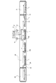
本発明の第2の実施形態の半田付け装置では、図4に示すように、1つの長いチャンバ40が使用されている。なおこの実施形態の構成要素のうち、第1の実施の形態の構成要素と同一のものには、同一符号を付して、その説明を省略する。
In the soldering apparatus of the second embodiment of the present invention, one
このチャンバ40内を図示しない搬送手段によって半田付け処理物1が矢印でしめす搬送経路に沿って搬送される。チャンバ40内には、還元性ガス、例えば水素ガス、または不活性ガス、例えば窒素ガスが充填され、その圧力はほぼ大気圧とされている。
The
このチャンバ40内における半田付け処理物1の搬送経路に沿って順に予熱ヒータ28、加熱ヒータ30a、30bが配置されている。この加熱ヒータ30aを挟んで予熱ヒータ28と反対側に、即ち加熱ヒータ30bの位置に真空チャンバ42が配置されている。この真空チャンバ42は、昇降装置44によってチャンバ40内において昇降可能に構成されている。真空チャンバ42が上昇している状態において、加熱ヒータ30aによって加熱されて、半田6の溶融温度近くまで加熱された半田付け処理物1が加熱ヒータ30bの上に、即ち真空チャンバ42の下方に搬送される。加熱ヒータ30bは、半田6の溶融温度以上の温度とされる。その搬送後に、真空チャンバ42がその内部に半田付け処理物1を収容するように真空チャンバ42が降下させられ、付属している真空ポンプ46によって真空チャンバ42内の排気が行われ、溶融している半田6内のボイドを膨張させて、溶融半田6中からボイドが抜かれる。その後に、真空ポンプ46を停止させて、真空チャンバ42に付属しているガス供給源47から還元性ガスまたは不活性ガスを導入して、真空チャンバ42内の圧力をほぼ大気圧まで上昇させる。これによって半田付け処理物1の周囲の圧力は、大気圧に戻り、溶融半田6中にボイドが残存していると、圧縮される。真空チャンバ42の降下後の、真空ポンプ46の作動、停止及びガス供給源47からの還元性ガスまたは不活性ガスの導入は、複数回に渡って行う。その後に、真空チャンバ42を上昇させて、半田付け処理物1は、側方に搬送され、冷却盤34上に搬送され、ここで冷却される。真空チャンバ42及びこれに付属する真空ポンプ46及びガス供給源47が圧力変更手段を構成している。なお、このチャンバ40の前側と後側には、それぞれロードロックチャンバ10、18が設けられ、ゲート20、20を介してチャンバ40と結合されている。ロードロックチャンバ18、20は、第1の実施の形態におけるロードロックチャンバ10、18と同様に動作する。
A
上記の2つの実施の形態では、セラミック基板2の一方の面の配線パターンにICチップ4を半田付けする例を示したが、図5に示すように、セラミック基板2におけるICチップ4とは反対側の面にヒートシンク48も半田50によって半田付けする場合にも、この発明を実施することができる。この場合にも、溶融されている半田50内に発生したボイドを抜くことができる。また、セラミック基板とICチップ以外でも、少なくとも2つの部品を半田付けする場合に、この発明を実施することができる。また、不活性ガスとしては、窒素を使用したが、これ以外にも公知の種々の不活性ガスを使用することができるし、還元性ガスも、水素以外の公知の種々のものを使用することができる。また、上記の実施の形態では、ボイドを膨張させる際、圧力をほぼ大気圧から約133Pa以下の真空にまで変化させたが、ボイドが適切に膨張するなら、約133Pa以下の真空まで圧力を下げる必要はない。また、上記の2つの実施形態では、半田付け処理を高速化するために、ロードロックチャンバ10、12を設けたが、場合によってはこれらを省略することもできるし、予熱ヒータ28を省略することもできる。
In the two embodiments described above, the example in which the IC chip 4 is soldered to the wiring pattern on one surface of the
1 半田付け処理物
2 基板(被半田付け体)
4 ICチップ(被半田付け体)
6 半田
30 加熱ヒータ(加熱手段)
34 冷却盤(冷却手段)
1
4 IC chip (object to be soldered)
6
34 Cooling panel (cooling means)
Claims (6)
前記半田の溶融状態において前記圧力を前記ほぼ大気圧から減圧し、その後に前記ほぼ大気圧の還元雰囲気または不活性雰囲気に戻す圧力変化過程と、
この圧力変化過程の後に、前記ほぼ大気圧の還元雰囲気または不活性雰囲気において前記半田付け処理物を冷却する冷却過程とを、
具備する半田付け方法。 In a reducing atmosphere or an inert atmosphere at a pressure of approximately atmospheric pressure, a soldering process product including a solder and a soldered body to be soldered by the solder is heated to melt the solder,
A pressure changing process in which the pressure is reduced from the substantially atmospheric pressure in the molten state of the solder and then returned to the reducing atmosphere or the inert atmosphere at the substantially atmospheric pressure;
After this pressure change process, a cooling process for cooling the soldered product in the reducing atmosphere or inert atmosphere at approximately atmospheric pressure,
Soldering method provided.
前記加熱チャンバは、
前記半田が溶融する温度に加熱する加熱手段と、
この加熱手段による加熱状態において前記加熱チャンバの圧力がほぼ大気圧の還元雰囲気または不活性雰囲気とし、その後に前記加熱チャンバを減圧し、再びほぼ大気圧の還元雰囲気または不活性雰囲気とする圧力調整手段とを、
具備し、
前記冷却チャンバは、ほぼ大気圧の還元雰囲気または不活性雰囲気中で前記半田付け処理物を冷却する冷却手段を有する
半田付け装置。 A soldering object including a solder and a soldered body to be soldered by the solder, and a heating chamber and a cooling chamber that are sequentially movable;
The heating chamber comprises:
Heating means for heating to a temperature at which the solder melts;
Pressure adjusting means in which the pressure of the heating chamber is reduced to an approximately atmospheric pressure reducing atmosphere or an inert atmosphere in the heating state by the heating means, and then the heating chamber is depressurized again to an approximately atmospheric pressure reducing atmosphere or an inert atmosphere. And
Equipped,
The said cooling chamber is a soldering apparatus which has a cooling means to cool the said soldering processed material in the reducing atmosphere or inert atmosphere of substantially atmospheric pressure.
前記搬送経路の中途に設けられ、前記被半田付け処理物を前記半田の溶融温度に加熱する加熱手段と、
この加熱手段による加熱状態において、前記半田付け処理物の周囲の圧力を減少させ、その後に前記チャンバ内の圧力に戻す圧力変更手段と、
前記加熱手段よりも後方の搬送経路において、前記半田付け処理物を冷却する冷却手段とを、
具備する半田付け装置。 A reducing atmosphere or an inert gas atmosphere having a pressure of approximately atmospheric pressure, and a chamber in which a soldering object including a solder and an object to be soldered to be soldered by the solder is conveyed along a conveying path;
A heating means provided in the middle of the conveyance path, for heating the soldering object to the melting temperature of the solder;
In the heating state by this heating means, a pressure changing means for reducing the pressure around the soldering object and then returning it to the pressure in the chamber;
A cooling means for cooling the soldered product in a transport path behind the heating means;
Soldering device provided.
Priority Applications (1)
| Application Number | Priority Date | Filing Date | Title |
|---|---|---|---|
| JP2005186111A JP2007000915A (en) | 2005-06-27 | 2005-06-27 | Soldering method and soldering device |
Applications Claiming Priority (1)
| Application Number | Priority Date | Filing Date | Title |
|---|---|---|---|
| JP2005186111A JP2007000915A (en) | 2005-06-27 | 2005-06-27 | Soldering method and soldering device |
Publications (2)
| Publication Number | Publication Date |
|---|---|
| JP2007000915A true JP2007000915A (en) | 2007-01-11 |
| JP2007000915A5 JP2007000915A5 (en) | 2008-08-07 |
Family
ID=37686975
Family Applications (1)
| Application Number | Title | Priority Date | Filing Date |
|---|---|---|---|
| JP2005186111A Pending JP2007000915A (en) | 2005-06-27 | 2005-06-27 | Soldering method and soldering device |
Country Status (1)
| Country | Link |
|---|---|
| JP (1) | JP2007000915A (en) |
Cited By (15)
| Publication number | Priority date | Publication date | Assignee | Title |
|---|---|---|---|---|
| JP2009130123A (en) * | 2007-11-22 | 2009-06-11 | Toyota Motor Corp | Bonding method of electronic component and circuit board, bonding device for the same, and semiconductor device |
| WO2012164776A1 (en) * | 2011-05-30 | 2012-12-06 | 有限会社ヨコタテクニカ | Soldering device |
| CN103681363A (en) * | 2012-09-17 | 2014-03-26 | Psk有限公司 | Serial thermal linear processor arrangement |
| US8962792B2 (en) | 2010-09-30 | 2015-02-24 | Dow Global Technologies Llc | Process for preparing epoxy resins |
| US9080059B2 (en) | 2010-09-30 | 2015-07-14 | Blue Cube Ip Llc | Coating compositions |
| US9284434B2 (en) | 2010-09-30 | 2016-03-15 | Blue Cube Ip Llc | Epoxy resin compositions |
| US9371414B2 (en) | 2010-09-30 | 2016-06-21 | Blue Cube Ip Llc | Epoxy resin adducts and thermosets thereof |
| JP2016140870A (en) * | 2015-01-30 | 2016-08-08 | 株式会社タムラ製作所 | Method for forming a solder bump |
| JP2016155141A (en) * | 2015-02-24 | 2016-09-01 | 株式会社タムラ製作所 | Method for manufacturing solder joint structure |
| JP2016157766A (en) * | 2015-02-24 | 2016-09-01 | 株式会社タムラ製作所 | Reflow method for solder bump |
| JP2020064937A (en) * | 2018-10-16 | 2020-04-23 | トヨタ自動車株式会社 | Method of manufacturing semiconductor device |
| JP2021507812A (en) * | 2017-12-29 | 2021-02-25 | シャンドン ツァイジュー エレクトロニック テクノロジー カンパニー リミテッド | Vacuum welding furnace for a wide range |
| JP2021508602A (en) * | 2017-12-29 | 2021-03-11 | シャンドン ツァイジュー エレクトロニック テクノロジー カンパニー リミテッド | Vacuum welding furnace and welding method |
| CN117139941A (en) * | 2023-10-30 | 2023-12-01 | 北京中科同志科技股份有限公司 | Vacuum system and working method thereof |
| DE112018006631B4 (en) | 2017-12-29 | 2024-08-29 | Shandong Caiju Electronic Technology Co., Ltd | Control system and control method for operating a vacuum brazing furnace |
Citations (2)
| Publication number | Priority date | Publication date | Assignee | Title |
|---|---|---|---|---|
| JPS54114455A (en) * | 1978-02-24 | 1979-09-06 | Kanto Yakin Kogyo | Furnace for soldering aluminium material under protecting gas without using flux and use |
| JP2003297860A (en) * | 2002-03-29 | 2003-10-17 | Fuji Electric Co Ltd | Method of manufacturing semiconductor device |
-
2005
- 2005-06-27 JP JP2005186111A patent/JP2007000915A/en active Pending
Patent Citations (2)
| Publication number | Priority date | Publication date | Assignee | Title |
|---|---|---|---|---|
| JPS54114455A (en) * | 1978-02-24 | 1979-09-06 | Kanto Yakin Kogyo | Furnace for soldering aluminium material under protecting gas without using flux and use |
| JP2003297860A (en) * | 2002-03-29 | 2003-10-17 | Fuji Electric Co Ltd | Method of manufacturing semiconductor device |
Cited By (19)
| Publication number | Priority date | Publication date | Assignee | Title |
|---|---|---|---|---|
| JP2009130123A (en) * | 2007-11-22 | 2009-06-11 | Toyota Motor Corp | Bonding method of electronic component and circuit board, bonding device for the same, and semiconductor device |
| US9284434B2 (en) | 2010-09-30 | 2016-03-15 | Blue Cube Ip Llc | Epoxy resin compositions |
| US9371414B2 (en) | 2010-09-30 | 2016-06-21 | Blue Cube Ip Llc | Epoxy resin adducts and thermosets thereof |
| US8962792B2 (en) | 2010-09-30 | 2015-02-24 | Dow Global Technologies Llc | Process for preparing epoxy resins |
| US9080059B2 (en) | 2010-09-30 | 2015-07-14 | Blue Cube Ip Llc | Coating compositions |
| WO2012164776A1 (en) * | 2011-05-30 | 2012-12-06 | 有限会社ヨコタテクニカ | Soldering device |
| JP2012245553A (en) * | 2011-05-30 | 2012-12-13 | Yokota Technica:Kk | Soldering device |
| JP2014060401A (en) * | 2012-09-17 | 2014-04-03 | Psk Inc | Arrangement of continuous linear thermal treatment apparatus |
| CN103681363A (en) * | 2012-09-17 | 2014-03-26 | Psk有限公司 | Serial thermal linear processor arrangement |
| JP2016140870A (en) * | 2015-01-30 | 2016-08-08 | 株式会社タムラ製作所 | Method for forming a solder bump |
| JP2016155141A (en) * | 2015-02-24 | 2016-09-01 | 株式会社タムラ製作所 | Method for manufacturing solder joint structure |
| JP2016157766A (en) * | 2015-02-24 | 2016-09-01 | 株式会社タムラ製作所 | Reflow method for solder bump |
| JP2021507812A (en) * | 2017-12-29 | 2021-02-25 | シャンドン ツァイジュー エレクトロニック テクノロジー カンパニー リミテッド | Vacuum welding furnace for a wide range |
| JP2021508602A (en) * | 2017-12-29 | 2021-03-11 | シャンドン ツァイジュー エレクトロニック テクノロジー カンパニー リミテッド | Vacuum welding furnace and welding method |
| JP7127132B2 (en) | 2017-12-29 | 2022-08-29 | シャンドン ツァイジュー エレクトロニック テクノロジー カンパニー リミテッド | Vacuum welding furnace and welding method |
| JP7181297B2 (en) | 2017-12-29 | 2022-11-30 | シャンドン ツァイジュー エレクトロニック テクノロジー カンパニー リミテッド | Wide-ranging vacuum welding furnace |
| DE112018006631B4 (en) | 2017-12-29 | 2024-08-29 | Shandong Caiju Electronic Technology Co., Ltd | Control system and control method for operating a vacuum brazing furnace |
| JP2020064937A (en) * | 2018-10-16 | 2020-04-23 | トヨタ自動車株式会社 | Method of manufacturing semiconductor device |
| CN117139941A (en) * | 2023-10-30 | 2023-12-01 | 北京中科同志科技股份有限公司 | Vacuum system and working method thereof |
Similar Documents
| Publication | Publication Date | Title |
|---|---|---|
| JP2007000915A (en) | Soldering method and soldering device | |
| US6905063B2 (en) | Method of manufacturing semiconductor device | |
| TWI492347B (en) | Apparatus for heat fusion treatment and the method thereof | |
| KR101049427B1 (en) | Soldering method | |
| JP5343566B2 (en) | Joining method and reflow apparatus | |
| JP2008153337A (en) | Method and device for separating laminated substrate, and computer readable recording medium with program recorded thereon | |
| JP2007000915A5 (en) | ||
| MXPA02004579A (en) | Method and device for producing a soldered joint. | |
| JP2010219158A (en) | Reflow soldering method | |
| JP2008182120A (en) | Method and device for soldering, and manufacturing method of semiconductor device | |
| JP2009115413A (en) | Heat-treatment apparatus | |
| WO2007088695A1 (en) | Soldering apparatus, soldering method and method for manufacturing semiconductor device | |
| JP2023518120A (en) | Systems for connecting electronic assemblies | |
| JP2010161207A (en) | Soldering method and soldering equipment | |
| JP2008229660A (en) | Soldering device | |
| JP2015082630A (en) | Soldering method by powder solder, and fluxless continuous reflow furnace | |
| JP3043435B2 (en) | Reflow soldering apparatus and reflow soldering method | |
| JP2007131466A (en) | Method and apparatus for manufacturing optical lens | |
| JP2009226456A (en) | Manufacturing method and joining apparatus of joined structure | |
| JP2011054865A (en) | Reflow device and reflow method | |
| JP6675622B1 (en) | Electronic component sintering apparatus and method | |
| JP2007053245A (en) | Method and device for soldering | |
| WO2022190450A1 (en) | Resin molding apparatus and method for producing resin molded article | |
| JP2023183115A (en) | Soldering device | |
| JP2004119664A (en) | Method and device for joining |
Legal Events
| Date | Code | Title | Description |
|---|---|---|---|
| A521 | Written amendment |
Free format text: JAPANESE INTERMEDIATE CODE: A523 Effective date: 20080623 |
|
| A621 | Written request for application examination |
Free format text: JAPANESE INTERMEDIATE CODE: A621 Effective date: 20080623 |
|
| A977 | Report on retrieval |
Free format text: JAPANESE INTERMEDIATE CODE: A971007 Effective date: 20100903 |
|
| A131 | Notification of reasons for refusal |
Free format text: JAPANESE INTERMEDIATE CODE: A131 Effective date: 20100914 |
|
| A02 | Decision of refusal |
Free format text: JAPANESE INTERMEDIATE CODE: A02 Effective date: 20110208 |