JP2006520104A - Immersion lithography method using carbon dioxide - Google Patents
Immersion lithography method using carbon dioxide Download PDFInfo
- Publication number
- JP2006520104A JP2006520104A JP2006508689A JP2006508689A JP2006520104A JP 2006520104 A JP2006520104 A JP 2006520104A JP 2006508689 A JP2006508689 A JP 2006508689A JP 2006508689 A JP2006508689 A JP 2006508689A JP 2006520104 A JP2006520104 A JP 2006520104A
- Authority
- JP
- Japan
- Prior art keywords
- immersion
- layer
- photoresist layer
- carbon dioxide
- fluid
- Prior art date
- Legal status (The legal status is an assumption and is not a legal conclusion. Google has not performed a legal analysis and makes no representation as to the accuracy of the status listed.)
- Pending
Links
Images


Classifications
-
- G—PHYSICS
- G03—PHOTOGRAPHY; CINEMATOGRAPHY; ANALOGOUS TECHNIQUES USING WAVES OTHER THAN OPTICAL WAVES; ELECTROGRAPHY; HOLOGRAPHY
- G03F—PHOTOMECHANICAL PRODUCTION OF TEXTURED OR PATTERNED SURFACES, e.g. FOR PRINTING, FOR PROCESSING OF SEMICONDUCTOR DEVICES; MATERIALS THEREFOR; ORIGINALS THEREFOR; APPARATUS SPECIALLY ADAPTED THEREFOR
- G03F7/00—Photomechanical, e.g. photolithographic, production of textured or patterned surfaces, e.g. printing surfaces; Materials therefor, e.g. comprising photoresists; Apparatus specially adapted therefor
- G03F7/70—Microphotolithographic exposure; Apparatus therefor
- G03F7/70216—Mask projection systems
- G03F7/70341—Details of immersion lithography aspects, e.g. exposure media or control of immersion liquid supply
-
- G—PHYSICS
- G03—PHOTOGRAPHY; CINEMATOGRAPHY; ANALOGOUS TECHNIQUES USING WAVES OTHER THAN OPTICAL WAVES; ELECTROGRAPHY; HOLOGRAPHY
- G03F—PHOTOMECHANICAL PRODUCTION OF TEXTURED OR PATTERNED SURFACES, e.g. FOR PRINTING, FOR PROCESSING OF SEMICONDUCTOR DEVICES; MATERIALS THEREFOR; ORIGINALS THEREFOR; APPARATUS SPECIALLY ADAPTED THEREFOR
- G03F7/00—Photomechanical, e.g. photolithographic, production of textured or patterned surfaces, e.g. printing surfaces; Materials therefor, e.g. comprising photoresists; Apparatus specially adapted therefor
- G03F7/20—Exposure; Apparatus therefor
- G03F7/2041—Exposure; Apparatus therefor in the presence of a fluid, e.g. immersion; using fluid cooling means
-
- G—PHYSICS
- G03—PHOTOGRAPHY; CINEMATOGRAPHY; ANALOGOUS TECHNIQUES USING WAVES OTHER THAN OPTICAL WAVES; ELECTROGRAPHY; HOLOGRAPHY
- G03F—PHOTOMECHANICAL PRODUCTION OF TEXTURED OR PATTERNED SURFACES, e.g. FOR PRINTING, FOR PROCESSING OF SEMICONDUCTOR DEVICES; MATERIALS THEREFOR; ORIGINALS THEREFOR; APPARATUS SPECIALLY ADAPTED THEREFOR
- G03F7/00—Photomechanical, e.g. photolithographic, production of textured or patterned surfaces, e.g. printing surfaces; Materials therefor, e.g. comprising photoresists; Apparatus specially adapted therefor
- G03F7/26—Processing photosensitive materials; Apparatus therefor
- G03F7/30—Imagewise removal using liquid means
- G03F7/32—Liquid compositions therefor, e.g. developers
Landscapes
- Physics & Mathematics (AREA)
- General Physics & Mathematics (AREA)
- Exposure Of Semiconductors, Excluding Electron Or Ion Beam Exposure (AREA)
- Exposure And Positioning Against Photoresist Photosensitive Materials (AREA)
- Photosensitive Polymer And Photoresist Processing (AREA)
Abstract
二酸化炭素を使用して基板上のフォトレジスト層に対して浸漬リソグラフィを実施することによって、基板にパターン形成される。二酸化炭素を使用して、浸漬層の提供および/または除去を行うことができ、および/またはフォトレジスト層の現像、乾燥、および/または除去を行うことができる。浸漬層は、液体および/または固体の浸漬層を含むことができる。これによって、浸漬リソグラフィにおける有機溶媒の必要性を軽減または解消することができる。The substrate is patterned by performing immersion lithography on the photoresist layer on the substrate using carbon dioxide. Carbon dioxide can be used to provide and / or remove the immersion layer and / or to develop, dry, and / or remove the photoresist layer. The immersion layer can include a liquid and / or solid immersion layer. This can reduce or eliminate the need for organic solvents in immersion lithography.
Description
本発明は、基板上のフォトレジスト層にパターン形成する方法、およびフォトレジスト層から浸漬層を除去する方法に関する。 The present invention relates to a method for patterning a photoresist layer on a substrate and a method for removing an immersion layer from a photoresist layer.
パーソナルコンピュータなど、より速くより小さい電子デバイスへの要求が増加し続けているのに応えるため、チップの寸法を大きくすることなくチップ上のトランジスタなどのマイクロエレクトロニクスデバイスの数を増加させることが望ましくなってきている。したがって、マイクロエレクトロニクスデバイスの寸法を減少させるための努力を続けることが望まれている。 In response to the ever-increasing demand for smaller electronic devices, such as personal computers, it is desirable to increase the number of microelectronic devices such as transistors on the chip without increasing the size of the chip. It is coming. Accordingly, it is desirable to continue efforts to reduce the dimensions of microelectronic devices.
このように非常に求められているマイクロエレクトロニクスデバイスの寸法減少を実現するための主要な障害の1つは、フォトリソグラフィの領域である。数十年の間、マイクロエレクトロニクスデバイスの製造においてフォトレジストにパターン形成するためにフォトリソグラフィが利用されてきた。フォトリソグラフィを使用してフォトレジスト層に形成される画像の解像度は、一般に、放射線源(λ)の波長に正比例し、フォトリソグラフィ装置の開口数(NA)に反比例する。したがって、フォトリソグラフィ装置によってパターン形成することが可能な特徴の寸法を減少させるために、より短い波長を有する放射線源の使用、および/またはより大きい開口数を有するフォトリソグラフィ装置の開発が望ましいと思われる。 One of the major obstacles to achieving such a very demanding microelectronic device size reduction is the area of photolithography. For decades, photolithography has been used to pattern photoresists in the manufacture of microelectronic devices. The resolution of an image formed in a photoresist layer using photolithography is generally directly proportional to the wavelength of the radiation source (λ) and inversely proportional to the numerical aperture (NA) of the photolithography apparatus. Accordingly, it would be desirable to use a radiation source having a shorter wavelength and / or develop a photolithographic apparatus having a larger numerical aperture in order to reduce the size of features that can be patterned by the photolithographic apparatus. It is.
波長を水銀g線(436nm)から、エキシマレーザーを使用して193nmまで、さらには157nmまで減少させる努力が行われてきた。X線リソグラフィおよび/または極紫外(EUV)リソグラフィを使用して放射線源の波長をさらに短縮させるための研究が現在も行われている。放射線源の波長を減少させ続けるコストは莫大なものとなり得る。フォトマスクおよび/レンズのための新しい材料を開発する必要があると思われる。波長が短くなると、フォトリソグラフィ方法を、屈折型フォトリソグラフィから反射型フォトリソグラフィに移行する必要性が生じ得る。一般にミラーはレンズよりも変動の自由度が少ないため、リソグラフィ品質の画像形成を実現する全反射型カメラの設計は、屈折画像形成系の設計よりも困難になり得る。 Efforts have been made to reduce the wavelength from mercury g-line (436 nm) to 193 nm and even 157 nm using an excimer laser. Research is ongoing to further reduce the wavelength of the radiation source using X-ray lithography and / or extreme ultraviolet (EUV) lithography. The cost of continuing to reduce the wavelength of the radiation source can be enormous. There appears to be a need to develop new materials for photomasks and / or lenses. As the wavelength becomes shorter, there may be a need to move photolithography methods from refractive photolithography to reflective photolithography. Since mirrors generally have less freedom of variation than lenses, the design of a totally reflective camera that achieves lithography quality imaging can be more difficult than the design of a refractive imaging system.
これらの課題から、マイクロエレクトロニクスデバイス製造と生物学との間で興味深い共通点が得られた。基準倍率を超えて顕微鏡レンズの解像度を増加させる問題に直面したとき、生物学者は、レンズと検査するスライドとの間に油層を設けることを始めた。この技術は、油浸顕微鏡法として知られており、レンズのガラスと空気との間の屈折率差によって生じる画質低下が軽減される。理想的状況においては、油の屈折率をガラスの屈折率と正確に一致させることで、画質低下を解消することができる。 These challenges created interesting similarities between microelectronic device manufacturing and biology. When faced with the problem of increasing the resolution of the microscope lens beyond the reference magnification, biologists began to place an oil layer between the lens and the slide to be examined. This technique is known as oil immersion microscopy and reduces image quality degradation caused by the refractive index difference between the lens glass and air. In an ideal situation, image quality degradation can be eliminated by making the refractive index of oil exactly match the refractive index of glass.
油浸顕微鏡法の原理を使用して、フォトリソグラフィ技術者は、浸漬リソグラフィとして知られるようになっている領域の探求を始めた。浸漬リソグラフィにおいては、最終光学素子とパターン形成すべき基板との間の空間に、高屈折率媒体が少なくとも部分的に充填される。M.SwitkesおよびM.Rothschild,「Immersion Lithography at 157 nm」,J.Vac.Sci.Technol.B、19(6):2353−2356(Nov/Dec 2001)では、油および潤滑剤として広く利用されている市販のパーフルオロポリエーテル(PFPE)類の使用が提案されており、例えば浸漬干渉リソグラフィ系中の高屈折率媒体として商品名Fomblin(登録商標)(ソルベイ・ソレクシス・コーポレーション(Solvay Solexis Corp.))が市販されている。SwitkesおよびRothschildは、パターン形成された基板からそれらを除去するためにFomblin(登録商標)PFS−1などの有機溶媒を使用している。SwitkesおよびRothschildの刊行物は、それらが完全に本明細書において説明されているかのように本明細書に組み入れられる。 Using the principles of oil immersion microscopy, photolithography engineers have begun exploring areas that have become known as immersion lithography. In immersion lithography, the space between the final optical element and the substrate to be patterned is at least partially filled with a high refractive index medium. M.M. Switches and M.M. Rothschild, “Immersion Lithography at 157 nm”, J. Am. Vac. Sci. Technol. B, 19 (6): 2353-2356 (Nov / Dec 2001) proposes the use of commercially available perfluoropolyethers (PFPE), which are widely used as oils and lubricants, for example immersion interference lithography. The brand name Fomblin (registered trademark) (Solvay Solexis Corp.) is commercially available as a high refractive index medium in the system. Switches and Rothschild use organic solvents such as Fomblin® PFS-1 to remove them from the patterned substrate. The Switzes and Rothschild publications are incorporated herein as if they were fully described herein.
浸漬リソグラフィは、光学の次の次世代リソグラフィを必要とせずに集積回路デバイスの集積密度を増加させ続けることができるブレイクスルー技術であると見なされている。例えば、Mark LaPedusによる「’Liquid Immersion’ could delay post−optical lithography,says MIT」の表題が付けられた刊行物,Semiconductor Business News,March 11,2002、および「What’s Next:Full Immersion Lithography?」と表題が付けられた刊行物,Solid State Technology,May 2002,Vol.45,No.5,p.24を参照されたい。 Immersion lithography is considered a breakthrough technique that can continue to increase the integration density of integrated circuit devices without the need for the next generation of optics lithography. For example, a publication entitled “'Liquid Immersion'” cull delay post-optical lithium, says MIT, by Semiconductor LaPedus, Semiconductor inductor, s 1, 11, 2 ” Publication titled “Solid State Technology, May 2002, Vol. 45, no. 5, p. See 24.
本発明の実施形態は、二酸化炭素を使用して基板上のフォトレジスト層に対して浸漬リソグラフィを実施することによる、基板にパターン形成する方法を提供する。本発明のある実施形態によると、浸漬リソグラフィ工程の種々のステップにおいて超臨界および/または液体の二酸化炭素使用することができる。その結果、浸漬流体を付着(deposit)
させるため、浸漬流体を除去するため、および/または浸漬リソグラフィにおける種々の他のステップを実施するために従来使用されてきた一部または全ての溶媒の代わりに使用できることができることが分かった。浸漬フォトリソグラフィにおける有機溶媒の使用は、浸漬リソグラフィ工程に対して環境的および/または経済的に大きな影響を有し得る。対照的に、本発明の実施形態では、このような有機溶媒の必要性を軽減または解消することができる。
Embodiments of the present invention provide a method for patterning a substrate by performing immersion lithography on a photoresist layer on the substrate using carbon dioxide. According to certain embodiments of the invention, supercritical and / or liquid carbon dioxide can be used in various steps of the immersion lithography process. As a result, the immersion fluid is deposited.
It has been found that it can be used in place of some or all of the solvents conventionally used to remove immersion fluid, and / or to perform various other steps in immersion lithography. The use of organic solvents in immersion photolithography can have a significant environmental and / or economic impact on the immersion lithography process. In contrast, embodiments of the present invention can reduce or eliminate the need for such organic solvents.
本発明のある実施形態においては、フォトレジスト層上に浸漬層を提供するステップと、浸漬層を通してフォトレジスト層に画像形成するステップと、フォトレジスト層から浸漬層を除去するステップと、浸漬層が除去されたフォトレジスト層を現像するステップと、浸漬層が除去されたフォトレジスト層を乾燥させるステップと、現像されたフォトレジスト層を使用して基板にパターン形成するステップと、パターン形成された基板からフォトレジスト層を除去するステップとによって、基板上のフォトレジスト層に対して浸漬リソグラフィが行われる。本発明の実施形態によると、浸漬層を提供するステップ、浸漬層を除去するステップ、フォトレジスト層を現像するステップ、フォトレジスト層を乾燥させるステップ、およびフォトレジスト層を除去するステップの1つ以上のステップが二酸化炭素を使用して実施される。 In certain embodiments of the invention, providing an immersion layer on the photoresist layer; imaging the photoresist layer through the immersion layer; removing the immersion layer from the photoresist layer; Developing the removed photoresist layer, drying the photoresist layer from which the immersion layer has been removed, patterning the substrate using the developed photoresist layer, and a patterned substrate Immersion lithography is performed on the photoresist layer on the substrate by removing the photoresist layer from the substrate. According to embodiments of the present invention, one or more of providing an immersion layer, removing the immersion layer, developing the photoresist layer, drying the photoresist layer, and removing the photoresist layer These steps are performed using carbon dioxide.
ある実施形態においては、フォトレジスト層上に浸漬層を提供するときに二酸化炭素が使用される。ある実施形態においては、フォトレジスト層上に流体層を付着させるが、この流体層は、二酸化炭素と少なくとも1種類の浸漬化合物とを含む。次に、二酸化炭素の少なくとも一部が流体層から除去されて、フォトレジスト層上に浸漬流体層が形成される。 In some embodiments, carbon dioxide is used when providing an immersion layer on the photoresist layer. In some embodiments, a fluid layer is deposited on the photoresist layer, the fluid layer including carbon dioxide and at least one immersion compound. Next, at least a portion of the carbon dioxide is removed from the fluid layer to form an immersion fluid layer on the photoresist layer.
別の実施形態においては、フォトレジスト層から浸漬層を除去するために二酸化炭素が使用される。これらの実施形態の一部では、フォトレジスト層の上に浸漬層が形成され、浸漬層を通してフォトレジスト層に画像形成される。液体および/または超臨界の二酸化炭素を含む浸漬リンス組成物と浸漬層を接触させることによって、画像形成されたフォトレジストから浸漬層が除去される。 In another embodiment, carbon dioxide is used to remove the immersion layer from the photoresist layer. In some of these embodiments, an immersion layer is formed over the photoresist layer and imaged through the immersion layer into the photoresist layer. The immersion layer is removed from the imaged photoresist by contacting the immersion layer with an immersion rinse composition comprising liquid and / or supercritical carbon dioxide.
さらに別の実施形態においては、フォトレジスト層を乾燥させるために二酸化炭素が使用される。ある実施形態においては、フォトレジスト層の上に浸漬層が形成され、浸漬層を通してフォトレジスト層に画像形成され、フォトレジスト層から浸漬層が除去される。浸漬層が除去されたフォトレジスト層は、液体および/または超臨界の二酸化炭素を使用して乾燥される。 In yet another embodiment, carbon dioxide is used to dry the photoresist layer. In some embodiments, an immersion layer is formed over the photoresist layer, imaged through the immersion layer to the photoresist layer, and the immersion layer is removed from the photoresist layer. The photoresist layer from which the immersion layer has been removed is dried using liquid and / or supercritical carbon dioxide.
さらに別の実施形態においては、フォトレジスト層を現像するために二酸化炭素が使用される。特に、ある実施形態においては、フォトレジスト層の上に浸漬層が形成され、浸漬層を通してフォトレジスト層に画像形成され、フォトレジスト層から浸漬層が除去される。浸漬層が除去されたフォトレジスト層は、液体および/または超臨界の二酸化炭素を使用して現像される。別の実施形態においては、液体および/または超臨界の二酸化炭素を使用して、フォトレジスト層から浸漬層が除去され、同時に、フォトレジスト層が現像される。 In yet another embodiment, carbon dioxide is used to develop the photoresist layer. In particular, in some embodiments, an immersion layer is formed on the photoresist layer, imaged through the immersion layer to the photoresist layer, and the immersion layer is removed from the photoresist layer. The photoresist layer with the immersion layer removed is developed using liquid and / or supercritical carbon dioxide. In another embodiment, the immersion layer is removed from the photoresist layer using liquid and / or supercritical carbon dioxide and, at the same time, the photoresist layer is developed.
本発明のさらに別の実施形態においては、フォトレジスト層の除去、および/または基板がパターン形成された後の基板の洗浄に二酸化炭素が使用される。特に、ある実施形態においては、フォトレジスト層の上に浸漬層が形成され、浸漬層を通してフォトレジスト層に画像形成され、フォトレジスト層から浸漬層が除去される。浸漬層が除去されたフォトレジスト層は現像され、現像されたフォトレジスト層を使用して基板にパターン形成される。次に、液体および/または超臨界の二酸化炭素を使用して、パターン形成された基板からフォトレジスト層が除去される。 In yet another embodiment of the invention, carbon dioxide is used to remove the photoresist layer and / or clean the substrate after the substrate has been patterned. In particular, in some embodiments, an immersion layer is formed on the photoresist layer, imaged through the immersion layer to the photoresist layer, and the immersion layer is removed from the photoresist layer. The photoresist layer from which the immersion layer has been removed is developed and patterned on the substrate using the developed photoresist layer. Next, the photoresist layer is removed from the patterned substrate using liquid and / or supercritical carbon dioxide.
さらに別の実施形態においては、固体浸漬膜が、フォトレジスト層の上に配置され(フォトレジスト層と接触させられ)、固体浸漬膜を通してフォトレジスト層に画像形成される。ある実施形態においては、固体浸漬膜は、二酸化炭素と、少なくとも1種類の固体浸漬膜化合物とを含む。しかし、別の実施形態においては、固体浸漬膜が二酸化炭素を含む必要がない。さらに、さらに別の実施形態においては、フォトレジスト層の上に最初に浸漬流体層が形成され、続いて、フォトレジスト層とは反対側の浸漬流体層の上に固体浸漬膜が配置される。固体浸漬膜とフォトレジスト層との間の浸漬流体層は、固体浸漬膜とフォトレジスト層との間の接触を改善することができる。ある実施形態においては、浸漬流体層が二酸化炭素を含むことができるが、別の実施形態においては二酸化炭素を含む必要はない。したがって、本発明のある実施形態は、介在する浸漬流体層が存在するまたは存在しない浸漬リソグラフィにおいて、固体浸漬膜(本明細書において接触浸漬膜とも記載する)の使用を提供する。 In yet another embodiment, a solid immersion film is placed over (in contact with) the photoresist layer and imaged through the solid immersion film into the photoresist layer. In certain embodiments, the solid immersion membrane comprises carbon dioxide and at least one solid immersion membrane compound. However, in another embodiment, the solid immersion membrane need not contain carbon dioxide. In yet another embodiment, an immersion fluid layer is first formed on the photoresist layer, followed by a solid immersion film disposed on the immersion fluid layer opposite the photoresist layer. An immersion fluid layer between the solid immersion film and the photoresist layer can improve contact between the solid immersion film and the photoresist layer. In some embodiments, the immersion fluid layer can include carbon dioxide, but in other embodiments it need not include carbon dioxide. Accordingly, certain embodiments of the present invention provide for the use of solid immersion films (also referred to herein as contact immersion films) in immersion lithography with or without an intervening immersion fluid layer.
本発明の実施形態を示す添付の図面を参照しながら、以下に本発明をより詳細に説明する。しかし、本明細書において説明される実施形態に限定されるものとして、本発明が構成されるべきではない。むしろ、本開示が徹底的および完全であり、本発明の範囲を当業者に完全に伝えられるように、これらの実施形態は提供される。図面において、層および領域の厚さは、明確にする目的で誇張している。全体にわたって類似の番号は類似の要素であることを意味する。層、領域、または基板などの要素が「上」にある、または別の要素の「上に向かって」延在すると記載される場合、他の要素の直接上にある、または直接上に向かって延在することができるし、あるいは介在する要素が存在してもよい。対照的に、ある要素が他の要素の「直接上に」ある、または「直接上に向かって」延在すると記載される場合は、介在する要素が存在しない。 The invention will be described in more detail below with reference to the accompanying drawings which show embodiments of the invention. However, the invention should not be constructed as limited to the embodiments described herein. Rather, these embodiments are provided so that this disclosure will be thorough and complete, and will fully convey the scope of the invention to those skilled in the art. In the drawings, the thickness of layers and regions are exaggerated for clarity. Like numbers throughout are meant to be like elements. When an element such as a layer, region, or substrate is described as being “on” or extending “above” another element, it is directly above or directly above another element There may be intervening elements that may extend. In contrast, when an element is described as being “directly above” or extending “directly above” another element, there are no intervening elements present.
図1は、本発明の実施形態により基板にパターン形成する方法の流れ図であり、本発明の種々の実施形態によりパターン形成される基板の断面図を含んでおり、これらの断面図は流れ図のブロックに対応している。ここで図1を参照すると、二酸化炭素を使用して基板上のフォトレジスト層に対して浸漬リソグラフィを実施することによる本発明の実施形態により、基板にパターン形成される。図1に示されるように、基板100は、半導体基板100aを含むことができ、さらに半導体基板100aの上に1つ以上の層100bを含むこともできる。当業者には周知であるが、半導体基板100aは、単結晶、単一元素および/または化合物の半導体基板を含むことができ、並びに/またはその上にエピタキシャル層などの単結晶、単一元素および/または化合物の半導体層を含むことができる。層100bは、二酸化ケイ素、窒化ケイ素、および/または他の従来の絶縁層などの1つ以上の絶縁層、金属および/またはドープされたポリシリコン層などの1つ以上の伝導層、および/またはマイクロエレクトロニクスデバイスの製造に使用されるあらゆる他の従来の層を含むことができる。半導体基板100aのパターン形成および/または層100bのパターン形成などの基板のパターン形成を行うために、従来技術を使用して基板100上にフォトレジスト層110が設けられる。
FIG. 1 is a flowchart of a method for patterning a substrate according to embodiments of the present invention, including cross-sectional views of the substrate patterned according to various embodiments of the present invention, these cross-sectional views being block diagrams. It corresponds to. Referring now to FIG. 1, a substrate is patterned according to an embodiment of the present invention by performing immersion lithography on a photoresist layer on a substrate using carbon dioxide. As shown in FIG. 1, the
ブロック130を参照すると、本明細書においては浸漬流体層とも記載される浸漬層120が、フォトレジスト層110の上に設けられる。本発明のある実施形態においては、二酸化炭素132を使用し、流体層をフォトレジスト層110の上に付着することによって、浸漬層120が設けられ、この流体層は二酸化炭素と少なくとも1種類の浸漬化合物とを含む。次に、二酸化炭素の少なくとも一部が流体層から除去されて、フォトレジスト層110の上に浸漬流体層120が形成される。ある実施形態においては、この流体層が、液体および/または超臨界の二酸化炭素を含む。別の実施形態においては、少なくとも1種類の浸漬流体化合物が、フッ素および/またはケイ素を含有する化合物、例えばパーフルオロポリエーテル化合物を含む。別の実施形態においては、少なくとも1種類の浸漬流体化合物がポリマーを含む。以下に多くの例が示される。
Referring to block 130, an
また図1を参照すると、ブロック140において、フォトレジスト層が、浸漬層を通して画像形成されて、画像形成されたフォトレジスト層110aが得られる。画像形成は、前述のSwitkesおよびRothschildの刊行物などに記載されるような公知の浸漬リソグラフィ法を使用して実施することができる。続いて、ブロック150において、画像形成されたフォトレジスト層110aから浸漬層120が除去される。ある実施形態においては、ブロック150における画像形成されたフォトレジスト層110aから浸漬層120を除去する工程中にCO2152が使用される。特に、ある実施形態においては、後に詳述するように、液体および/または超臨界の二酸化炭素を含む浸漬リンス組成物と浸漬層を接触させる。
Referring also to FIG. 1, at
また図1を参照すると、ブロック160において、フォトレジスト層110bを現像して乾燥させると、パターン形成されたフォトレジスト層110cが得られる。ある実施形態においては、フォトレジスト層の現像および/または乾燥の工程中にCO2162が使用される。特に、ある実施形態においては、浸漬層が除去されたフォトレジスト層が、液体および/または超臨界の二酸化炭素を使用して乾燥される。さらに別の実施形態においては、浸漬層が除去されたフォトレジスト層が、液体および/または超臨界の二酸化炭素162を使用して現像される。さらに別の実施形態においては、フォトレジスト層の現像および乾燥のために二酸化炭素が使用される。さらに別の実施形態においては、フォトレジスト層の現像および乾燥を同時に行うために二酸化炭素が使用される。二酸化炭素を使用してフォトレジストの乾燥および/または現像を行う技術は当業者に公知であるので、本明細書においてさらに説明する必要はない。
Referring also to FIG. 1, in
また図1を参照すると、ブロック170において、ウェットエッチングおよび/またはドライエッチングなどの従来のパターン形成技術を使用して、基板にパターン形成される。これによって、パターン形成された層100cが得られる。次に、ブロック180において、パターン形成されフォトレジスト層110cが除去される。本発明のある実施形態においては、パターン形成されたフォトレジスト層110cを基板100から除去するために、液体および/または超臨界の二酸化炭素が使用される。二酸化炭素を使用してフォトレジストを除去する技術は当業者に公知であるので、本明細書においてさらに説明する必要はない。
Referring also to FIG. 1, in
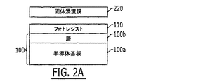
図2A〜2Bは、本発明によりフォトレジスト層の上に浸漬層を提供する(図1のブロック130)別の実施形態を説明する断面図である。図2Aに示されるように、固体浸漬膜220をフォトレジスト層110の上に配置(接触)させることで、図2Bに示される固体浸漬膜が形成される。固体浸漬膜220の組成については後述する。固体浸漬膜220は、固体薄膜を基板上に配置する標準的技術を使用して取り付けることができる。ある実施形態においては、固体浸漬膜220が、二酸化炭素と少なくとも1種類の固体浸漬膜化合物とを含む。続いて、ブロック130と関連して前述したように、固体浸漬膜から二酸化炭素が除去される。別の実施形態においては、浸漬リソグラフィ工程における基板のパターン形成のために、CO2を使用せずに、固体浸漬膜を使用することができる。したがって、この工程において二酸化炭素を使用しても使用しなくても、固浸リソグラフィを行うことができる。
2A-2B are cross-sectional views illustrating another embodiment for providing an immersion layer over a photoresist layer according to the present invention (block 130 of FIG. 1). As shown in FIG. 2A, the
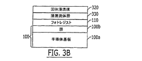
図3A〜3Bは、本発明のさらに別の実施形態による浸漬リソグラフィ方法の断面図である。これらの実施形態においては、固体浸漬膜320(図2Aの固体浸漬膜220と類似のものであってもよい)と、フォトレジスト110との間に浸漬流体層330が配置されることで、接触が促進され、および/または固体浸漬膜320とフォトレジスト110との間により均一な光学界面が形成される。図3Bは、フォトレジスト110上の固体浸漬膜320を示しており、これらの間に浸漬流体層330を有する。ある実施形態においては、固体浸漬膜320は、浸漬流体層320よりも実質的に厚く、そのため浸漬リソグラフィのパラメータは、主として固体浸漬膜320によって決定される。別の実施形態においては、異なる厚さの比を使用することができる。さらに別の実施形態においては、固体浸漬膜320および液浸層330の使用を、CO2を伴わない浸漬リソグラフィ方法において使用することができる。次に、従来の浸漬リソグラフィおよび/または図1の浸漬リソグラフィを図2Bおよび/または3Bの実施形態に対して実施できることを理解されたい。
3A-3B are cross-sectional views of an immersion lithography method according to yet another embodiment of the present invention. In these embodiments, the
これより、本発明の種々の実施形態のさらなる議論について以下に説明する。 A further discussion of various embodiments of the present invention will now be described below.
本発明のある実施形態によると、基板上のフォトレジスト層にパターン形成する方法は、二酸化炭素と少なくとも1種類の浸漬化合物とを含む流体層をフォトレジスト層の上に付着させるステップと、流体層から二酸化炭素を除去してフォトレジスト層上に浸漬流体層を形成するステップとを含む。 According to an embodiment of the present invention, a method of patterning a photoresist layer on a substrate includes depositing a fluid layer comprising carbon dioxide and at least one immersion compound on the photoresist layer; Removing carbon dioxide from the substrate to form an immersion fluid layer on the photoresist layer.
当業者に周知の種々の方法によって、フォトレジスト層の上に流体層を付着させることができる。例えば、ある実施形態においては、基板の上に浸漬流体がスピンコーティングされる。別の実施形態においては、溶媒中に溶解させた浸漬流体が基板上にスピンコーティングされ、この溶媒がCO2を含む。別の実施形態においては、浸漬コーティングおよび/またはナイフコーティングなどのフリーメニスカスコーティング方法を使用することができる。 The fluid layer can be deposited over the photoresist layer by a variety of methods well known to those skilled in the art. For example, in some embodiments, an immersion fluid is spin coated onto the substrate. In another embodiment, the immersion fluid dissolved in a solvent is spin-coated on a substrate, the solvent comprises CO 2. In another embodiment, free meniscus coating methods such as dip coating and / or knife coating can be used.
二酸化炭素は、液相、気相、または超臨界相であってよい。液体CO2が使用される場合、ある実施形態においては、その工程中に使用される温度は31℃未満となる。気体CO2が使用される場合、その相を高圧で使用することができる。本明細書において使用される場合、用語「高圧」は、一般に約50〜約500bar(約5MPa〜約50MPa)の圧力を有するCO2を意味する。ある実施形態においては、CO2が「超臨界」相で使用される。本明細書において使用される場合、「超臨界」は、流体媒体がその臨界温度および臨界圧力より上にある、すなわちCO2の場合約31℃(約304.15K)および約71bar(約7.1MPa)より上にあることを意味する。CO2の熱力学性質は、Hyatt,J.Org.Chem.49:5097−5101(1984)に報告されており、これによるとCO2の臨界温度が約31℃であると記載されており、したがって本発明のある実施形態においては31℃(304.15K)を超える温度で実施することができる。本発明の目的では、約20(約2MPa)または約50bar(約5MPa)の下限から約200bar(約20MPa)または約1000bar(約100MPa)の上限までの範囲の圧力のCO2を使用することができる。 Carbon dioxide may be in the liquid phase, the gas phase, or the supercritical phase. When liquid CO 2 is used, in some embodiments, the temperature used during the process will be less than 31 ° C. If gaseous CO 2 is used, the phase can be used at high pressure. As used herein, the term “high pressure” generally means CO 2 having a pressure of about 50 to about 500 bar (about 5 MPa to about 50 MPa). In some embodiments, CO 2 is used in the “supercritical” phase. As used herein, "supercritical" is a fluid medium is above its critical temperature and critical pressure, i.e., about 31 ° C. For CO 2 (approximately 304.15K) and about 71Bar (about 7. 1 MPa). The thermodynamic properties of CO 2 are described in Hyatt, J. et al. Org. Chem. 49: 5097-5101 (1984), which states that the critical temperature of CO 2 is about 31 ° C., and thus in one embodiment of the invention 31 ° C. (304.15 K). Can be carried out at temperatures above. For the purposes of the present invention, it is possible to use CO 2 at a pressure ranging from a lower limit of about 20 (about 2 MPa) or about 50 bar (about 5 MPa) to an upper limit of about 200 bar (about 20 MPa) or about 1000 bar (about 100 MPa). it can.
浸漬流体化合物は、限定するものではないがパーフルオロポリエーテルおよび他の好適なフッ素化化合物などの種々の浸漬流体化合物から選択することができる。他の好適なフッ素化化合物としては、フルオロアルキル(メタ)アクリレートのホモポリマーおよびコポリマー、ならびに、テトラフルオロエチレン、ヘキサフルオロプロピレン、ペンタフルオロジメチルジオキソール、ノルボルネン、フッ化ビニリデン、およびノルボルネン誘導体のホモポリマーおよびコポリマーを挙げることができ、例えば国際公開第00/17712号パンフレットおよび第00/67072号パンフレットに記載されている。この材料は、ケイ素またはシロキサン単位、例えばポリジメチルシロキサンまたはポリジアルキルシランを含むこともできる。これらの材料はCO2可溶性となることができ、CO2中に置かれて可溶性にすることができる。一般に、浸漬流体化合物は、最終光学素子と、マイクロエレクトロニクス工作物との間に少なくとも10μmの作業距離を得るのに十分透明となるべきである。画像形成を妨害するほど浸漬流体化合物がフォトレジストと相互作用すべきではない。さらに、浸漬流体化合物は、クリーンルーム環境および半導体製造工程に対して適合性であるべきである。ある実施形態においては、浸漬流体化合物が非毒性である、および/または化学的に不活性である。 The immersion fluid compound can be selected from a variety of immersion fluid compounds such as, but not limited to, perfluoropolyethers and other suitable fluorinated compounds. Other suitable fluorinated compounds include homopolymers and copolymers of fluoroalkyl (meth) acrylates and homopolymers of tetrafluoroethylene, hexafluoropropylene, pentafluorodimethyldioxole, norbornene, vinylidene fluoride, and norbornene derivatives. Polymers and copolymers may be mentioned, for example as described in WO 00/17712 and 00/67072. The material can also contain silicon or siloxane units, such as polydimethylsiloxane or polydialkylsilane. These materials can become CO 2 soluble and can be placed in CO 2 to make it soluble. In general, the immersion fluid compound should be sufficiently transparent to obtain a working distance of at least 10 μm between the final optical element and the microelectronic workpiece. Immersion fluid compounds should not interact with the photoresist to interfere with image formation. Furthermore, the immersion fluid compound should be compatible with clean room environments and semiconductor manufacturing processes. In some embodiments, the immersion fluid compound is non-toxic and / or chemically inert.
別の実施形態においては、浸漬流体は、架橋PFPEフィルムなどの架橋材料を含む前述の材料から誘導することができる高透明度材料の接触膜の形態を取ってもよい。さらに別の実施形態においては、浸漬流体は、前述の接触膜の形態を取り、前述の種類の液浸層が介在してもよい。 In another embodiment, the immersion fluid may take the form of a contact film of a highly transparent material that can be derived from the aforementioned materials, including cross-linked materials such as cross-linked PFPE films. In yet another embodiment, the immersion fluid takes the form of a contact film as described above and may be interspersed with an immersion layer of the type described above.
ある実施形態においては、浸漬流体化合物は、フォトリソグラフィに使用される供給源からの放射線(例えば、レーザー)による損傷に対して抵抗性である。放射線源による損傷に対する浸漬流体化合物の抵抗性は、対象の放射線源に曝露した後の化合物の透過率の変化を測定することによって求めることができる。例えば、浸漬流体化合物の層を、2つのCaF2窓の間に配置し、0.3mJ/cm2−パルスのフルエンスにおいて100J/cmなどの標準線量を使用して157nmで放射線照射し、その化合物の透過率の変化を測定することができる。ある実施形態、特に、複数の曝露に浸漬流体化合物が使用される実施形態においては、透過率の変化を50%未満とすることができ、別の実施形態においては25%未満とすることができる。浸漬流体化合物が、対象の放射線源による損傷に対して抵抗性であることが好ましいが、本発明の浸漬流体化合物は、対象の放射線源によって容易に損傷される場合でも使用することが可能である。これらの場合において、1、2、3、4、または5回の曝露後に浸漬流体化合物を交換することができる。例えば、対象の放射線源によって容易に損傷される浸漬流体化合物を、ウエハとともに移動させて、各曝露場において新しい浸漬流体化合物を供給することができる。 In certain embodiments, the immersion fluid compound is resistant to damage from radiation (eg, a laser) from a source used for photolithography. The resistance of an immersion fluid compound to damage by a radiation source can be determined by measuring the change in the transmittance of the compound after exposure to the subject radiation source. For example, a layer of immersion fluid compound is placed between two CaF 2 windows and irradiated at 157 nm using a standard dose such as 100 J / cm at a fluence of 0.3 mJ / cm 2 -pulse, and the compound The change in transmittance can be measured. In some embodiments, particularly those in which immersion fluid compounds are used for multiple exposures, the change in transmission can be less than 50%, and in other embodiments it can be less than 25%. . Although it is preferred that the immersion fluid compound be resistant to damage by the subject radiation source, the immersion fluid compound of the present invention can be used even when easily damaged by the subject radiation source. . In these cases, the immersion fluid compound can be changed after 1, 2, 3, 4, or 5 exposures. For example, an immersion fluid compound that is easily damaged by the radiation source of interest can be moved with the wafer to provide a new immersion fluid compound at each exposure field.
限定するものではないが、流体層の圧力の低下、および/または流体層の温度の上昇などの当業者に周知の種々の方法によって、流体層から二酸化炭素を除去して浸漬流体層を形成することができる。マイクロエレクトロニクス工作物は典型的には熱量を有するので、ある実施形態においては、流体層の圧力を低下させることによって流体層から二酸化炭素を除去することが望ましい場合がある。 Carbon dioxide is removed from the fluid layer to form an immersion fluid layer by various methods well known to those skilled in the art, such as, but not limited to, reducing the pressure of the fluid layer and / or increasing the temperature of the fluid layer. be able to. Because microelectronic workpieces typically have an amount of heat, in some embodiments it may be desirable to remove carbon dioxide from the fluid layer by reducing the fluid layer pressure.
ある実施形態においては、浸漬流体層の屈折率は、画像形成装置の光学素子の屈折率の10〜20%以内となるべきである。例えば、CaF2光学素子(n=1.56、式中のnは屈折率である)が画像形成装置中に使用される場合、浸漬流体化合物は1.25または1.40の下限と1.72または1.87の上限との間の屈折率を有することができる。 In some embodiments, the refractive index of the immersion fluid layer should be within 10-20% of the refractive index of the optical element of the image forming device. For example, if a CaF 2 optical element (n = 1.56, where n is the refractive index) is used in the image forming apparatus, the immersion fluid compound has a lower limit of 1.25 or 1.40 and 1. It can have a refractive index between 72 or 1.87 upper limit.
ある実施形態においては、本発明によりフォトレジスト層にパターン形成する方法は、浸漬流体層を付着させるステップの前に、フォトレジスト層を上に有する基板を二酸化炭素チャンバーに入れるステップを含む。この二酸化炭素チャンバーは、前述の液体または超臨界の二酸化炭素を使用して加工する場合の圧力および温度に耐えることができるチャンバーである。二酸化炭素チャンバーはトラックの上にあってもよい。当業者には周知のように、マイクロエレクトロニクスデバイスは、トラック上の一群の工具を使用して製造することができる。本発明のある実施形態により浸漬リソグラフィを実施するために、トラックにCO2チャンバーを付け加えることができる。 In certain embodiments, a method of patterning a photoresist layer according to the present invention includes placing a substrate having the photoresist layer thereon into a carbon dioxide chamber prior to depositing the immersion fluid layer. This carbon dioxide chamber is a chamber that can withstand the pressure and temperature when processing using the aforementioned liquid or supercritical carbon dioxide. The carbon dioxide chamber may be on the track. As is well known to those skilled in the art, microelectronic devices can be manufactured using a group of tools on a track. A CO 2 chamber can be added to the track to perform immersion lithography according to an embodiment of the present invention.
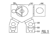
ある実施形態においては、二酸化炭素チャンバーは、図5に示されるようなマイクロエレクトロニクスデバイス加工装置の一部である。この装置は、1つ以上の半導体ウエハ530(半導体基板)が搭載されたカセット520を有するロードロックチャンバー510を含む。ロードロックチャンバー510は、トランスファーチャンバー560と連結される。トランスファーチャンバー560は装置内の第1のチャンバーから装置内の第2のチャンバーに半導体ウエハ530を移動させるために使用することができる。図5に示されるトランスファーチャンバー560は、半導体ウエハ530の搭載および取り外しのためにロボットアーム550を有するが、半導体ウエハ530の搭載および取り外しのための種々の手段を利用できることを理解されたい。図5に示されるように、トランスファーチャンバー560が二酸化炭素チャンバー540に連結されている。
In some embodiments, the carbon dioxide chamber is part of a microelectronic device processing apparatus as shown in FIG. The apparatus includes a
本発明のある実施形態においては、フォトレジスト層にパターン形成する方法は、浸漬流体層を浸漬リンス組成物と接触させるステップを含む(図1のブロック150)。浸漬流体層と浸漬リンス組成物との接触は、限定するものではないがCFC、HCFC、HFC、およびFC、あるいは非分子エッチャント、PFP溶媒、またはフルオロエーテルなどの溶媒を使用したリンスなどの当業者に周知の種々の方法によって実施することができる。ある実施形態においては、浸漬流体層と浸漬リンス組成物との接触が二酸化炭素チャンバー内で実施される。この二酸化炭素チャンバーは、前述の液体または超臨界の二酸化炭素を使用して加工する場合の圧力および温度に耐えることができるチャンバーである。ある実施形態においては、二酸化炭素チャンバーがトラック上にある。二酸化炭素チャンバーが浸漬流体層の付着に使用され、二酸化炭素チャンバーが浸漬流体層の除去に使用される場合、浸漬流体層の付着に使用される二酸化炭素チャンバーは、浸漬流体層の除去に使用される二酸化炭素チャンバーと同じであってもよいし、または異なる二酸化炭素チャンバーであってもよい。 In some embodiments of the present invention, the method of patterning a photoresist layer includes contacting the immersion fluid layer with an immersion rinse composition (block 150 of FIG. 1). Contact between the immersion fluid layer and the immersion rinse composition is not limited to those skilled in the art, such as, but not limited to, CFC, HCFC, HFC, and FC, or rinse using a solvent such as non-molecular etchant, PFP solvent, or fluoroether Can be carried out by various known methods. In some embodiments, contacting the immersion fluid layer with the immersion rinse composition is performed in a carbon dioxide chamber. This carbon dioxide chamber is a chamber that can withstand the pressure and temperature when processing using the aforementioned liquid or supercritical carbon dioxide. In some embodiments, the carbon dioxide chamber is on the track. If a carbon dioxide chamber is used for the deposition fluid layer deposition and the carbon dioxide chamber is used for removal of the immersion fluid layer, the carbon dioxide chamber used for deposition fluid layer deposition is used for the removal of the immersion fluid layer. The carbon dioxide chamber may be the same, or may be a different carbon dioxide chamber.
浸漬リンス組成物は、パターン形成されたフォトレジスト層から全てまたは実質的に全ての浸漬流体層を除去することが可能な組成物である。浸漬リンス組成物は、水性組成物、有機組成物、または二酸化炭素系(例えば、50%を超える二酸化炭素を含む)組成物であってよい。前述のように、ある実施形態においては、浸漬リンス組成物が液体または超臨界の二酸化炭素を含む。 An immersion rinse composition is a composition that can remove all or substantially all of the immersion fluid layer from the patterned photoresist layer. The immersion rinse composition may be an aqueous composition, an organic composition, or a carbon dioxide-based (eg, containing more than 50% carbon dioxide) composition. As mentioned above, in certain embodiments, the immersion rinse composition comprises liquid or supercritical carbon dioxide.
ある実施形態においては、浸漬リンス組成物は、液体または超臨界の二酸化炭素と共溶媒とを含む。使用可能な共溶媒の例としては、アルコール(例えば、メタノール、エタノール、およびイソプロパノール);フッ素化溶媒および他のハロゲン化溶媒(例えば、クロロトリフルオロメタン、トリクロロフルオロメタン、パーフルオロプロパン、クロロジフルオロメタン、および六フッ化硫黄);アミン(例えば、N−メチルピロリドン);アミド(例えば、ジメチルアセトアミド);芳香族溶媒(例えば、ベンゼン、トルエン、およびキシレン);エステル(例えば、酢酸エチル、二塩基性エステル、および乳酸エステル);エーテル(例えば、ジエチルエーテル、テトラヒドロフラン、およびグリコールエーテル);脂肪族炭化水素(例えば、メタン、エタン、プロパン、アンモニウムブタン、n−ペンタン、およびヘキサン);酸化物(例えば、亜酸化窒素);オレフィン(例えば、エチレンおよびプロピレン);天然炭化水素(例えば、イソプレン、テルペン、およびd−リモネン);ケトン(例えば、アセトンおよびメチルエチルケトン);有機シリコーン;アルキルピロリドン(例えば、N−メチルピロリドン);パラフィン(例えば、イソパラフィン);石油系溶媒および溶媒混合物;ならびに利用可能で好適な他の相溶性溶媒または混合物が挙げられるが、これらに限定されるものではない。上記共溶媒の混合物を使用することもできる。 In certain embodiments, the immersion rinse composition comprises liquid or supercritical carbon dioxide and a cosolvent. Examples of co-solvents that can be used include alcohols (eg, methanol, ethanol, and isopropanol); fluorinated solvents and other halogenated solvents (eg, chlorotrifluoromethane, trichlorofluoromethane, perfluoropropane, chlorodifluoromethane, And amines (eg, N-methylpyrrolidone); amides (eg, dimethylacetamide); aromatic solvents (eg, benzene, toluene, and xylene); esters (eg, ethyl acetate, dibasic esters) Ethers (eg, diethyl ether, tetrahydrofuran, and glycol ethers); aliphatic hydrocarbons (eg, methane, ethane, propane, ammonium butane, n-pentane, and hexane); oxides Olefins (eg, ethylene and propylene); natural hydrocarbons (eg, isoprene, terpene, and d-limonene); ketones (eg, acetone and methyl ethyl ketone); organosilicones; alkyl pyrrolidones (eg, N -Methylpyrrolidone); paraffins (eg, isoparaffin); petroleum-based solvents and solvent mixtures; and other suitable compatible solvents or mixtures that may be used, but are not limited to. Mixtures of the above co-solvents can also be used.
本発明のさらに別の実施形態によると、基板上のフォトレジスト層にパターン形成する方法は、フォトレジスト層上に浸漬流体層を付着させるステップと、フォトレジスト層に画像形成して画像形成されたフォトレジスト層を得るステップと、液体または超臨界の二酸化炭素を含む浸漬リンス組成物と浸漬流体層を接触させて、画像形成されたフォトレジスト層から浸漬流体層を除去するステップとを含む。 According to yet another embodiment of the present invention, a method for patterning a photoresist layer on a substrate is imaged by depositing an immersion fluid layer on the photoresist layer and imaging the photoresist layer. Obtaining a photoresist layer and contacting the immersion fluid layer with an immersion rinse composition comprising liquid or supercritical carbon dioxide to remove the immersion fluid layer from the imaged photoresist layer.
浸漬流体層は、ブロック130において前述したようにしてフォトレジスト層の上に付着させることができる。浸漬流体層は、種々の浸漬流体化合物を含むことができ、例えばパーフルオロポリエーテルを含むことができるが、これに限定されるものではない。ある実施形態においては、浸漬流体層が、ニュージャージー州ソロフェア(Thorofare,New Jersey)のソルベイ・ソレクシス(Solvay Solexis)より市販されるFomblin(登録商標)Y(例えば、Fomblin(登録商標)Y−18またはFomblin(登録商標)Y−140)またはFomblin(登録商標)Z(例えば、Fomblin(登録商標)Z−25)である。別の実施形態においては、浸漬流体層が、前述のように二酸化炭素を使用して付着されたパーフルオロポリエーテルまたは他の好適なフッ素化化合物の層である。透明性、光学的欠陥がないこと、画像形成を妨害するレジストとの相互作用が最小限または存在しないこと、クリーンルーム環境および半導体製造工程への適合性、非毒性、化学的不活性、対象の放射線による損傷に対する抵抗性、および/または最終光学素子と一致した屈折率などの、浸漬流体化合物および浸漬流体層について前述した種々の特性の1つ以上と類似した特性を、浸漬流体化合物および/または浸漬流体層が有することができる。
The immersion fluid layer can be deposited over the photoresist layer as previously described in
浸漬流体層を付着させた後、種々の浸漬リソグラフィ法を使用してフォトレジスト層に画像形成することができる(ブロック140)。一般に、例えば、最終光学素子と半導体基板上のフォトレジスト層との間に浸漬流体層を導入することなどによって、「乾式」(すなわち、非浸漬)リソグラフィ装置を、浸漬リソグラフィ法に変換することができる。例えば、図4に示されるような、干渉リソグラフィシステム400についてこれより説明する。最終光学素子450と、フォトレジスト層を上に有する基板を含むマイクロエレクトロニクス工作物470との間に、浸漬流体層460が付着されており、フォトレジスト層が浸漬流体層と隣接していることを除けば、干渉リソグラフィシステム400は、当業者に周知の従来の干渉リソグラフィシステムであってよい。一般に、ラムダ−フィジック(Lambda−Physik)LPX−200 F2レーザーなどの放射線源410がレーザービーム420を放射する。CaF2などを含むことができる反射板430からの部分的な反射によって、レーザービーム420が2つの偏光したアームに分割される。次にこれらのアームは、Siなどを含むことができるミラー440で反射されて、最終的に最終光学素子450に入る。次に、これらのアームは浸漬流体層460を透過して、マイクロエレクトロニクス工作物470の表面で交差する。干渉リソグラフィシステムを参照しながら本発明の実施形態を説明してきたが、限定するものではないが投影リソグラフィおよび/または接触印刷リソグラフィなどの当業者に周知の種々のリソグラフィシステムを使用して本発明が実施可能であることを理解されたい。
After the immersion fluid layer is applied, various immersion lithography methods can be used to image the photoresist layer (block 140). In general, a “dry” (ie, non-immersion) lithographic apparatus can be converted to an immersion lithography method, such as by introducing an immersion fluid layer between the final optical element and a photoresist layer on a semiconductor substrate. it can. For example, an
フォトレジスト層の画像形成の後、前述したように浸漬層を浸漬リンス組成物と接触させることによって浸漬層が除去される(ブロック160)。 After imaging the photoresist layer, the immersion layer is removed by contacting the immersion layer with the immersion rinse composition as described above (block 160).
本発明の別の実施形態によると、基板上の画像形成されたフォトレジスト層から浸漬流体層を除去する方法は、液体または超臨界の二酸化炭素を含む浸漬リンス組成物と浸漬流体層を接触させて、画像形成されたフォトレジスト層から浸漬流体層を除去するステップを含む。この接触作業、浸漬流体層、および浸漬リンス組成物は、前述のものと類似していてもよい。 According to another embodiment of the present invention, a method for removing an immersion fluid layer from an imaged photoresist layer on a substrate comprises contacting the immersion fluid layer with an immersion rinse composition comprising liquid or supercritical carbon dioxide. Removing the immersion fluid layer from the imaged photoresist layer. This contact operation, immersion fluid layer, and immersion rinse composition may be similar to those described above.
さらに別の実施形態においては、前述したように、浸漬流体が付着され、フォトレジストに画像形成され、浸漬流体がリンスされて除去される。このフォトレジストは、例えばTMAHおよび/または他の従来の現像剤を使用して現像される。続いて、パターン形成されたフォトレジストは、CO2および/または界面活性剤を有するCO2を使用して乾燥される。CO2および/または界面活性剤を有するCO2を使用することによって、画像の崩壊を軽減または防止することができる。さらに別の実施形態においては、直接CO2を使用し、当業者に周知の技術を使用して、ネガ型またはポジ型の画像を現像することができる。 In yet another embodiment, as described above, immersion fluid is deposited, imaged on the photoresist, and immersion fluid is rinsed and removed. The photoresist is developed using, for example, TMAH and / or other conventional developers. Subsequently, the patterned photoresist is dried using CO 2 and / or CO 2 with a surfactant. By using CO 2 and / or CO 2 with a surfactant, image collapse can be reduced or prevented. In yet another embodiment, negative or positive images can be developed using direct CO 2 and techniques well known to those skilled in the art.
さらに別の実施形態においては、浸漬流体の適用および除去に非CO2方法を使用することができるが、続いて、パターンの現像のためにCO2を直接使用するか、標準的現像方法の後にCO2系乾燥方法を使用するかのいずれかによって、レジスト中のパターンの現像を補助するためにCO2を使用することができる。別の実施形態においては、フォトレジスト層の現像および浸漬層の除去を同時に行うためにCO2を使用することができる。さらに別の実施形態においては、前述したように、二酸化炭素を使用してフォトレジストの洗浄または除去が行われる。 In yet another embodiment, non-CO 2 methods can be used to apply and remove immersion fluid, but subsequently use CO 2 directly for pattern development or after standard development methods. by either the use of CO 2 based dry method, it is possible to use a CO 2 to assist the development of the pattern in the resist. In another embodiment, CO 2 can be used to simultaneously develop the photoresist layer and remove the immersion layer. In yet another embodiment, as described above, the photoresist is cleaned or removed using carbon dioxide.
さらに別の実施形態においては、浸漬流体は、ポリマーフィルムであり、二酸化炭素を使用または非使用で、フォトレジスト上に物理的に配置される。さらに別の実施形態においては、ポリマーフィルムとフォトレジストとの間に液体が配置され、配置の際、二酸化炭素は使用される場合と使用されない場合がある。 In yet another embodiment, the immersion fluid is a polymer film and is physically placed on the photoresist with or without carbon dioxide. In yet another embodiment, a liquid is placed between the polymer film and the photoresist, and carbon dioxide may or may not be used during placement.
本明細書において、本発明の実施形態を開示しており、特定の用語が使用されているが、それらは一般的および説明的な意味でのみ使用されており、請求項に記載される本発明の範囲を限定する目的で使用されているのではない。 Although embodiments of the present invention are disclosed herein and specific terms are used, they are used in a general and descriptive sense only, and the claimed invention It is not used for the purpose of limiting the range.
Claims (49)
二酸化炭素を使用して前記基板上のフォトレジスト層に対して浸漬リソグラフィを実施する工程を含む、方法。 A method of forming a pattern on a substrate,
Performing immersion lithography on the photoresist layer on the substrate using carbon dioxide.
前記フォトレジスト層上に浸漬層を提供するステップと、
前記浸漬層を通して前記フォトレジスト層に画像形成するステップと、
前記フォトレジスト層から前記浸漬層を除去するステップと、
前記浸漬層が除去された前記フォトレジスト層を現像するステップと、
前記浸漬層が除去された前記フォトレジスト層を乾燥させるステップと、
現像された前記フォトレジスト層を使用して前記基板にパターン形成するステップと、
パターン形成された前記基板から前記フォトレジスト層を除去するステップとを含み、
前記浸漬層を提供するステップ、前記浸漬層を除去するステップ、前記フォトレジスト層を現像するステップ、前記フォトレジスト層を乾燥させるステップ、および前記フォトレジスト層を除去するステップの1つ以上のステップが二酸化炭素を使用して実施される、請求項1に記載の方法。 Performing the immersion lithography on the photoresist layer on the substrate using carbon dioxide,
Providing an immersion layer on the photoresist layer;
Imaging the photoresist layer through the immersion layer;
Removing the immersion layer from the photoresist layer;
Developing the photoresist layer from which the immersion layer has been removed;
Drying the photoresist layer from which the immersion layer has been removed;
Patterning the substrate using the developed photoresist layer;
Removing the photoresist layer from the patterned substrate.
One or more of the steps of providing the immersion layer, removing the immersion layer, developing the photoresist layer, drying the photoresist layer, and removing the photoresist layer; The method of claim 1, wherein the method is performed using carbon dioxide.
前記フォトレジスト層の上に、二酸化炭素と少なくとも1種類の浸漬化合物とを含む流体層を付着させるステップと、
フォトレジスト層の上に浸漬流体層を形成するために、前記二酸化炭素の少なくとも一部を前記流体層から除去するステップとを含む、請求項1に記載の方法。 Performing the immersion lithography on the photoresist layer on the substrate using carbon dioxide,
Depositing a fluid layer comprising carbon dioxide and at least one immersion compound on the photoresist layer;
And removing at least a portion of the carbon dioxide from the fluid layer to form an immersion fluid layer over the photoresist layer.
前記フォトレジスト層の上に浸漬層を形成するステップと、
前記浸漬層を通して前記フォトレジスト層に画像形成するステップと、
液体および/または超臨界の二酸化炭素を含む浸漬リンス組成物と前記浸漬層を接触させることによって、前記画像形成されたフォトレジスト層から前記浸漬層を除去するステップとを含む、請求項1に記載の方法。 Said step of performing immersion lithography on a photoresist layer on a substrate using carbon dioxide,
Forming an immersion layer on the photoresist layer;
Imaging the photoresist layer through the immersion layer;
2. Removing the immersion layer from the imaged photoresist layer by contacting the immersion layer with an immersion rinse composition comprising a liquid and / or supercritical carbon dioxide. the method of.
前記フォトレジスト層の上に、二酸化炭素と少なくとも1種類の浸漬化合物とを含む流体層を付着させる段階と、
前記フォトレジスト層の上に前記浸漬層を形成するために、前記二酸化炭素を前記流体層から除去する段階とを含む、請求項11に記載の方法。 The step of forming the immersion layer comprises:
Depositing a fluid layer comprising carbon dioxide and at least one immersion compound on the photoresist layer;
12. The method of claim 11, comprising removing the carbon dioxide from the fluid layer to form the immersion layer over the photoresist layer.
前記フォトレジスト層の上に浸漬層を形成するステップと、
前記浸漬層を通して前記フォトレジスト層に画像形成するステップと、
前記フォトレジスト層から前記浸漬層を除去するステップと、
液体および/または超臨界の二酸化炭素を使用して、前記浸漬層が除去された前記フォトレジスト層を乾燥させるステップとを含む、請求項1に記載の方法。 Said step of performing immersion lithography on a photoresist layer on a substrate using carbon dioxide,
Forming an immersion layer on the photoresist layer;
Imaging the photoresist layer through the immersion layer;
Removing the immersion layer from the photoresist layer;
And drying the photoresist layer from which the immersion layer has been removed using liquid and / or supercritical carbon dioxide.
前記フォトレジスト層の上に浸漬層を形成するステップと、
前記浸漬層を通して前記フォトレジスト層に画像形成するステップと、
前記フォトレジスト層から前記浸漬層を除去するステップと、
液体および/または超臨界の二酸化炭素を使用して、前記浸漬層が除去された前記フォトレジスト層を現像するステップとを含む、請求項1に記載の方法。 Said step of performing immersion lithography on a photoresist layer on a substrate using carbon dioxide,
Forming an immersion layer on the photoresist layer;
Imaging the photoresist layer through the immersion layer;
Removing the immersion layer from the photoresist layer;
And developing the photoresist layer from which the immersion layer has been removed using liquid and / or supercritical carbon dioxide.
前記フォトレジスト層の上に浸漬層を形成するステップと、
前記浸漬層を通して前記フォトレジスト層に画像形成するステップと、
液体および/または超臨界の二酸化炭素を使用して、前記フォトレジスト層から前記浸漬層を除去し、同時に前記フォトレジスト層を現像するステップとを含む、請求項1に記載の方法。 Said step of performing immersion lithography on a photoresist layer on a substrate using carbon dioxide,
Forming an immersion layer on the photoresist layer;
Imaging the photoresist layer through the immersion layer;
Removing the immersion layer from the photoresist layer and simultaneously developing the photoresist layer using liquid and / or supercritical carbon dioxide.
前記フォトレジスト層の上に浸漬層を形成するステップと、
前記浸漬層を通して前記フォトレジスト層に画像形成するステップと、
前記フォトレジスト層から前記浸漬層を除去するステップと、
前記浸漬層が除去された前記フォトレジスト層を現像するステップと、
現像された前記フォトレジスト層を使用して前記基板にパターン形成するステップと、
液体および/または超臨界の二酸化炭素を使用して、パターン形成された前記基板から前記フォトレジスト層を除去するステップとを含む、請求項1に記載の方法。 Said step of performing immersion lithography on a photoresist layer on a substrate using carbon dioxide,
Forming an immersion layer on the photoresist layer;
Imaging the photoresist layer through the immersion layer;
Removing the immersion layer from the photoresist layer;
Developing the photoresist layer from which the immersion layer has been removed;
Patterning the substrate using the developed photoresist layer;
Removing the layer of photoresist from the patterned substrate using liquid and / or supercritical carbon dioxide.
前記フォトレジスト層の上に固体浸漬膜を配置するステップと
前記固体浸漬膜を通して前記フォトレジスト層に画像形成するステップとを含む、請求項1に記載の方法。 Said step of performing immersion lithography on a photoresist layer on a substrate using carbon dioxide,
The method of claim 1, comprising: placing a solid immersion film over the photoresist layer; and imaging the photoresist layer through the solid immersion film.
二酸化炭素と少なくとも1種類の固体浸漬膜化合物とを含む固体浸漬膜を前記フォトレジスト層の上に配置する段階と、
前記固体浸漬膜から前記二酸化炭素を除去する段階とを含む、請求項31に記載の方法。 Placing the solid immersion film on the photoresist layer comprises:
Disposing a solid immersion film comprising carbon dioxide and at least one solid immersion film compound on the photoresist layer;
32. The method of claim 31, comprising removing the carbon dioxide from the solid immersion membrane.
前記フォトレジスト層の上に二酸化炭素と少なくとも1種類の浸漬化合物とを含む流体層を付着させる段階と、
前記フォトレジスト層の上に浸漬流体層を形成するために、前記二酸化炭素の少なくとも一部を前記流体層から除去する段階とを含む、請求項33に記載の方法。 Placing said immersion fluid layer comprises:
Depositing a fluid layer comprising carbon dioxide and at least one immersion compound on the photoresist layer;
34. The method of claim 33, comprising: removing at least a portion of the carbon dioxide from the fluid layer to form an immersion fluid layer over the photoresist layer.
前記フォトレジスト層の上に配置された前記固体浸漬膜を通して前記フォトレジスト層に画像形成するステップとを含む、基板にパターン形成する方法。 Placing a solid immersion film over a photoresist layer on a substrate;
Imaging the photoresist layer through the solid immersion film disposed on the photoresist layer.
前記フォトレジスト層の上に、二酸化炭素と少なくとも1種類の浸漬化合物とを含む流体層を配置する段階と、
前記フォトレジスト層の上に浸漬流体層を形成するために、前記二酸化炭素の少なくとも一部を前記流体層から除去する段階とを含む、請求項42に記載の方法。 Placing said immersion fluid layer comprises:
Disposing on the photoresist layer a fluid layer comprising carbon dioxide and at least one immersion compound;
43. The method of claim 42, further comprising removing at least a portion of the carbon dioxide from the fluid layer to form an immersion fluid layer over the photoresist layer.
Applications Claiming Priority (2)
| Application Number | Priority Date | Filing Date | Title |
|---|---|---|---|
| US10/386,356 US7029832B2 (en) | 2003-03-11 | 2003-03-11 | Immersion lithography methods using carbon dioxide |
| PCT/US2004/003556 WO2004081666A1 (en) | 2003-03-11 | 2004-01-23 | Immersion lithography methods using carbon dioxide |
Publications (2)
| Publication Number | Publication Date |
|---|---|
| JP2006520104A true JP2006520104A (en) | 2006-08-31 |
| JP2006520104A5 JP2006520104A5 (en) | 2007-03-08 |
Family
ID=32961680
Family Applications (1)
| Application Number | Title | Priority Date | Filing Date |
|---|---|---|---|
| JP2006508689A Pending JP2006520104A (en) | 2003-03-11 | 2004-01-23 | Immersion lithography method using carbon dioxide |
Country Status (5)
| Country | Link |
|---|---|
| US (1) | US7029832B2 (en) |
| EP (1) | EP1602012A1 (en) |
| JP (1) | JP2006520104A (en) |
| TW (1) | TW200504864A (en) |
| WO (1) | WO2004081666A1 (en) |
Cited By (7)
| Publication number | Priority date | Publication date | Assignee | Title |
|---|---|---|---|---|
| JP2006189687A (en) * | 2005-01-07 | 2006-07-20 | Jsr Corp | Method for forming photoresist pattern, and substrate for forming the photoresist pattern |
| JP2006344960A (en) * | 2005-06-10 | 2006-12-21 | Internatl Business Mach Corp <Ibm> | Immersion lithography device and method (immersion lithography device having uniform pressure, at least on projection optical component and wafer) |
| JP2007513518A (en) * | 2003-12-03 | 2007-05-24 | アドバンスト・マイクロ・ディバイシズ・インコーポレイテッド | Immersion lithography process using adaptive immersion media |
| JP2008530789A (en) * | 2005-02-10 | 2008-08-07 | エーエスエムエル ネザーランズ ビー.ブイ. | Immersion liquid, exposure apparatus and exposure method |
| JP2008227548A (en) * | 2004-12-20 | 2008-09-25 | Asml Netherlands Bv | Lithographic apparatus and device manufacturing method |
| JP2009500828A (en) * | 2005-07-01 | 2009-01-08 | アドバンスト・マイクロ・ディバイシズ・インコーポレイテッド | Method and system for drying a wafer and cleaning a lens using a supercritical fluid in immersion lithography |
| JP2015029155A (en) * | 2004-06-09 | 2015-02-12 | 株式会社ニコン | Exposure device and device manufacturing method |
Families Citing this family (140)
| Publication number | Priority date | Publication date | Assignee | Title |
|---|---|---|---|---|
| JP3977324B2 (en) | 2002-11-12 | 2007-09-19 | エーエスエムエル ネザーランズ ビー.ブイ. | Lithographic apparatus |
| US9482966B2 (en) | 2002-11-12 | 2016-11-01 | Asml Netherlands B.V. | Lithographic apparatus and device manufacturing method |
| KR100588124B1 (en) | 2002-11-12 | 2006-06-09 | 에이에스엠엘 네델란즈 비.브이. | Lithographic Apparatus and Device Manufacturing Method |
| US7372541B2 (en) * | 2002-11-12 | 2008-05-13 | Asml Netherlands B.V. | Lithographic apparatus and device manufacturing method |
| US10503084B2 (en) | 2002-11-12 | 2019-12-10 | Asml Netherlands B.V. | Lithographic apparatus and device manufacturing method |
| WO2004053953A1 (en) * | 2002-12-10 | 2004-06-24 | Nikon Corporation | Exposure apparatus and method for manufacturing device |
| EP1571697A4 (en) * | 2002-12-10 | 2007-07-04 | Nikon Corp | Exposure system and device producing method |
| US7242455B2 (en) * | 2002-12-10 | 2007-07-10 | Nikon Corporation | Exposure apparatus and method for producing device |
| JP4352874B2 (en) * | 2002-12-10 | 2009-10-28 | 株式会社ニコン | Exposure apparatus and device manufacturing method |
| KR101085372B1 (en) * | 2002-12-10 | 2011-11-21 | 가부시키가이샤 니콘 | Exposure apparatus and method for manufacturing device |
| AU2003289271A1 (en) * | 2002-12-10 | 2004-06-30 | Nikon Corporation | Exposure apparatus, exposure method and method for manufacturing device |
| US7948604B2 (en) * | 2002-12-10 | 2011-05-24 | Nikon Corporation | Exposure apparatus and method for producing device |
| DE10261775A1 (en) | 2002-12-20 | 2004-07-01 | Carl Zeiss Smt Ag | Device for the optical measurement of an imaging system |
| TW200500813A (en) * | 2003-02-26 | 2005-01-01 | Nikon Corp | Exposure apparatus and method, and method of producing device |
| KR101181688B1 (en) | 2003-03-25 | 2012-09-19 | 가부시키가이샤 니콘 | Exposure system and device production method |
| JP4902201B2 (en) | 2003-04-07 | 2012-03-21 | 株式会社ニコン | Exposure apparatus, exposure method, and device manufacturing method |
| KR101177331B1 (en) * | 2003-04-09 | 2012-08-30 | 가부시키가이샤 니콘 | Immersion lithography fluid control system |
| SG2012050829A (en) | 2003-04-10 | 2015-07-30 | Nippon Kogaku Kk | Environmental system including vacuum scavange for an immersion lithography apparatus |
| JP4650413B2 (en) | 2003-04-10 | 2011-03-16 | 株式会社ニコン | Environmental system including a transfer area for an immersion lithography apparatus |
| JP4656057B2 (en) * | 2003-04-10 | 2011-03-23 | 株式会社ニコン | Electro-osmotic element for immersion lithography equipment |
| EP2921905B1 (en) * | 2003-04-10 | 2017-12-27 | Nikon Corporation | Run-off path to collect liquid for an immersion lithography apparatus |
| SG185136A1 (en) * | 2003-04-11 | 2012-11-29 | Nikon Corp | Cleanup method for optics in immersion lithography |
| WO2004092830A2 (en) * | 2003-04-11 | 2004-10-28 | Nikon Corporation | Liquid jet and recovery system for immersion lithography |
| KR101225884B1 (en) | 2003-04-11 | 2013-01-28 | 가부시키가이샤 니콘 | Apparatus and method for maintaining immersion fluid in the gap under the projection lens during wafer exchange in an immersion lithography machine |
| WO2004095135A2 (en) | 2003-04-17 | 2004-11-04 | Nikon Corporation | Optical arrangement of autofocus elements for use with immersion lithography |
| TWI295414B (en) | 2003-05-13 | 2008-04-01 | Asml Netherlands Bv | Lithographic apparatus and device manufacturing method |
| WO2004102646A1 (en) * | 2003-05-15 | 2004-11-25 | Nikon Corporation | Exposure apparatus and method for manufacturing device |
| TW200509205A (en) * | 2003-05-23 | 2005-03-01 | Nippon Kogaku Kk | Exposure method and device-manufacturing method |
| TWI470671B (en) | 2003-05-23 | 2015-01-21 | 尼康股份有限公司 | Exposure method and exposure apparatus, and device manufacturing method |
| KR101728664B1 (en) | 2003-05-28 | 2017-05-02 | 가부시키가이샤 니콘 | Exposure method, exposure device, and device manufacturing method |
| US7213963B2 (en) | 2003-06-09 | 2007-05-08 | Asml Netherlands B.V. | Lithographic apparatus and device manufacturing method |
| EP2261741A3 (en) | 2003-06-11 | 2011-05-25 | ASML Netherlands B.V. | Lithographic apparatus and device manufacturing method |
| US7317504B2 (en) * | 2004-04-08 | 2008-01-08 | Asml Netherlands B.V. | Lithographic apparatus and device manufacturing method |
| KR101940892B1 (en) * | 2003-06-13 | 2019-01-21 | 가부시키가이샤 니콘 | Exposure method, substrate stage, exposure apparatus and method for manufacturing device |
| KR101289979B1 (en) | 2003-06-19 | 2013-07-26 | 가부시키가이샤 니콘 | Exposure device and device producing method |
| US7236232B2 (en) * | 2003-07-01 | 2007-06-26 | Nikon Corporation | Using isotopically specified fluids as optical elements |
| EP2853943B1 (en) * | 2003-07-08 | 2016-11-16 | Nikon Corporation | Wafer table for immersion lithography |
| CN102944981A (en) * | 2003-07-09 | 2013-02-27 | 株式会社尼康 | Exposure apparatus, and device fabricating method |
| EP2264532B1 (en) | 2003-07-09 | 2012-10-31 | Nikon Corporation | Exposure apparatus and device manufacturing method |
| WO2005006418A1 (en) | 2003-07-09 | 2005-01-20 | Nikon Corporation | Exposure apparatus and method for manufacturing device |
| EP1650787A4 (en) * | 2003-07-25 | 2007-09-19 | Nikon Corp | Inspection method and inspection device for projection optical system, and production method for projection optical system |
| US7326522B2 (en) * | 2004-02-11 | 2008-02-05 | Asml Netherlands B.V. | Device manufacturing method and a substrate |
| US7175968B2 (en) * | 2003-07-28 | 2007-02-13 | Asml Netherlands B.V. | Lithographic apparatus, device manufacturing method and a substrate |
| EP1503244A1 (en) * | 2003-07-28 | 2005-02-02 | ASML Netherlands B.V. | Lithographic projection apparatus and device manufacturing method |
| EP2264534B1 (en) | 2003-07-28 | 2013-07-17 | Nikon Corporation | Exposure apparatus, method for producing device, and method for controlling exposure apparatus |
| US20050022731A1 (en) * | 2003-07-30 | 2005-02-03 | Bernard Petrillo | Immersion optics fluid dispenser |
| US7779781B2 (en) | 2003-07-31 | 2010-08-24 | Asml Netherlands B.V. | Lithographic apparatus and device manufacturing method |
| TWI263859B (en) | 2003-08-29 | 2006-10-11 | Asml Netherlands Bv | Lithographic apparatus and device manufacturing method |
| TWI245163B (en) | 2003-08-29 | 2005-12-11 | Asml Netherlands Bv | Lithographic apparatus and device manufacturing method |
| SG145780A1 (en) * | 2003-08-29 | 2008-09-29 | Nikon Corp | Exposure apparatus and device fabricating method |
| KR20170070264A (en) | 2003-09-03 | 2017-06-21 | 가부시키가이샤 니콘 | Apparatus and method for providing fluid for immersion lithography |
| WO2005029559A1 (en) * | 2003-09-19 | 2005-03-31 | Nikon Corporation | Exposure apparatus and device producing method |
| WO2005031824A1 (en) * | 2003-09-29 | 2005-04-07 | Nikon Corporation | Projection exposure device, projection exposure method, and device manufacturing method |
| TW201809911A (en) | 2003-09-29 | 2018-03-16 | 尼康股份有限公司 | Exposure apparatus, exposure method, and method for producing device |
| WO2005036623A1 (en) | 2003-10-08 | 2005-04-21 | Zao Nikon Co., Ltd. | Substrate transporting apparatus and method, exposure apparatus and method, and device producing method |
| KR101319109B1 (en) * | 2003-10-08 | 2013-10-17 | 가부시키가이샤 자오 니콘 | Substrate carrying apparatus, substrate carrying method, exposure apparatus, exposure method, and method for producing device |
| JP2005136364A (en) * | 2003-10-08 | 2005-05-26 | Zao Nikon Co Ltd | Substrate carrying device, exposure device and device manufacturing method |
| TWI598934B (en) | 2003-10-09 | 2017-09-11 | Nippon Kogaku Kk | Exposure apparatus, exposure method, and device manufacturing method |
| US7411653B2 (en) | 2003-10-28 | 2008-08-12 | Asml Netherlands B.V. | Lithographic apparatus |
| US7352433B2 (en) | 2003-10-28 | 2008-04-01 | Asml Netherlands B.V. | Lithographic apparatus and device manufacturing method |
| JP4295712B2 (en) | 2003-11-14 | 2009-07-15 | エーエスエムエル ネザーランズ ビー.ブイ. | Lithographic apparatus and apparatus manufacturing method |
| TWI440981B (en) | 2003-12-03 | 2014-06-11 | 尼康股份有限公司 | Exposure apparatus, exposure method, and device manufacturing method |
| KR101111363B1 (en) * | 2003-12-15 | 2012-04-12 | 가부시키가이샤 니콘 | Projection exposure apparatus, stage apparatus, and exposure method |
| US20070081133A1 (en) * | 2004-12-14 | 2007-04-12 | Niikon Corporation | Projection exposure apparatus and stage unit, and exposure method |
| KR101941351B1 (en) | 2003-12-15 | 2019-01-22 | 가부시키가이샤 니콘 | Stage system, exposure apparatus and exposure method |
| KR101376715B1 (en) | 2003-12-19 | 2014-03-27 | 더 유니버시티 오브 노쓰 캐롤라이나 엣 채플 힐 | Methods for fabricating isolated micro- and nano- structures using soft or imprint lithography |
| US7460206B2 (en) * | 2003-12-19 | 2008-12-02 | Carl Zeiss Smt Ag | Projection objective for immersion lithography |
| JP4323946B2 (en) * | 2003-12-19 | 2009-09-02 | キヤノン株式会社 | Exposure equipment |
| US7394521B2 (en) * | 2003-12-23 | 2008-07-01 | Asml Netherlands B.V. | Lithographic apparatus and device manufacturing method |
| JP4843503B2 (en) * | 2004-01-20 | 2011-12-21 | カール・ツァイス・エスエムティー・ゲーエムベーハー | Microlithographic projection exposure apparatus and measuring apparatus for projection lens |
| US7391501B2 (en) * | 2004-01-22 | 2008-06-24 | Intel Corporation | Immersion liquids with siloxane polymer for immersion lithography |
| US20050161644A1 (en) * | 2004-01-23 | 2005-07-28 | Peng Zhang | Immersion lithography fluids |
| TWI259319B (en) * | 2004-01-23 | 2006-08-01 | Air Prod & Chem | Immersion lithography fluids |
| US7589822B2 (en) | 2004-02-02 | 2009-09-15 | Nikon Corporation | Stage drive method and stage unit, exposure apparatus, and device manufacturing method |
| EP1713114B1 (en) | 2004-02-03 | 2018-09-19 | Nikon Corporation | Exposure apparatus and device manufacturing method |
| US7741012B1 (en) * | 2004-03-01 | 2010-06-22 | Advanced Micro Devices, Inc. | Method for removal of immersion lithography medium in immersion lithography processes |
| JP4220423B2 (en) | 2004-03-24 | 2009-02-04 | 株式会社東芝 | Resist pattern forming method |
| KR101851511B1 (en) | 2004-03-25 | 2018-04-23 | 가부시키가이샤 니콘 | Exposure apparatus and method for manufacturing device |
| US7898642B2 (en) * | 2004-04-14 | 2011-03-01 | Asml Netherlands B.V. | Lithographic apparatus and device manufacturing method |
| WO2005111722A2 (en) | 2004-05-04 | 2005-11-24 | Nikon Corporation | Apparatus and method for providing fluid for immersion lithography |
| JP3981368B2 (en) * | 2004-05-17 | 2007-09-26 | 松下電器産業株式会社 | Pattern formation method |
| US7616383B2 (en) * | 2004-05-18 | 2009-11-10 | Asml Netherlands B.V. | Lithographic apparatus and device manufacturing method |
| WO2005119368A2 (en) | 2004-06-04 | 2005-12-15 | Carl Zeiss Smt Ag | System for measuring the image quality of an optical imaging system |
| US7463330B2 (en) | 2004-07-07 | 2008-12-09 | Asml Netherlands B.V. | Lithographic apparatus and device manufacturing method |
| JP4894515B2 (en) | 2004-07-12 | 2012-03-14 | 株式会社ニコン | Exposure apparatus, device manufacturing method, and liquid detection method |
| JP4264038B2 (en) * | 2004-07-13 | 2009-05-13 | パナソニック株式会社 | Liquid for immersion exposure and pattern forming method |
| JP4983257B2 (en) * | 2004-08-18 | 2012-07-25 | 株式会社ニコン | Exposure apparatus, device manufacturing method, measuring member, and measuring method |
| US7701550B2 (en) | 2004-08-19 | 2010-04-20 | Asml Netherlands B.V. | Lithographic apparatus and device manufacturing method |
| US7209213B2 (en) * | 2004-10-07 | 2007-04-24 | Asml Netherlands B.V. | Lithographic apparatus and device manufacturing method |
| US7732123B2 (en) * | 2004-11-23 | 2010-06-08 | Taiwan Semiconductor Manufacturing Company, Ltd. | Immersion photolithography with megasonic rinse |
| US7397533B2 (en) | 2004-12-07 | 2008-07-08 | Asml Netherlands B.V. | Lithographic apparatus and device manufacturing method |
| SG124359A1 (en) * | 2005-01-14 | 2006-08-30 | Asml Netherlands Bv | Lithographic apparatus and device manufacturing method |
| SG124351A1 (en) | 2005-01-14 | 2006-08-30 | Asml Netherlands Bv | Lithographic apparatus and device manufacturing method |
| US8692973B2 (en) | 2005-01-31 | 2014-04-08 | Nikon Corporation | Exposure apparatus and method for producing device |
| KR101440617B1 (en) | 2005-01-31 | 2014-09-15 | 가부시키가이샤 니콘 | Exposure apparatus and method for manufacturing device |
| US7399581B2 (en) * | 2005-02-24 | 2008-07-15 | International Business Machines Corporation | Photoresist topcoat for a photolithographic process |
| US7282701B2 (en) * | 2005-02-28 | 2007-10-16 | Asml Netherlands B.V. | Sensor for use in a lithographic apparatus |
| USRE43576E1 (en) | 2005-04-08 | 2012-08-14 | Asml Netherlands B.V. | Dual stage lithographic apparatus and device manufacturing method |
| US7291850B2 (en) * | 2005-04-08 | 2007-11-06 | Asml Netherlands B.V. | Lithographic apparatus and device manufacturing method |
| US7927779B2 (en) | 2005-06-30 | 2011-04-19 | Taiwan Semiconductor Manufacturing Companym, Ltd. | Water mark defect prevention for immersion lithography |
| US20070002296A1 (en) * | 2005-06-30 | 2007-01-04 | Taiwan Semiconductor Manufacturing Company, Ltd. | Immersion lithography defect reduction |
| US7571992B2 (en) * | 2005-07-01 | 2009-08-11 | Xerox Corporation | Pressure compensation structure for microelectromechanical systems |
| US8383322B2 (en) | 2005-08-05 | 2013-02-26 | Taiwan Semiconductor Manufacturing Company, Ltd. | Immersion lithography watermark reduction |
| US7535644B2 (en) * | 2005-08-12 | 2009-05-19 | Asml Netherlands B.V. | Lens element, lithographic apparatus, device manufacturing method, and device manufactured thereby |
| US7357768B2 (en) * | 2005-09-22 | 2008-04-15 | William Marshall | Recliner exerciser |
| US7495743B2 (en) * | 2005-09-30 | 2009-02-24 | International Business Machines Corporation | Immersion optical lithography system having protective optical coating |
| US7993808B2 (en) | 2005-09-30 | 2011-08-09 | Taiwan Semiconductor Manufacturing Company, Ltd. | TARC material for immersion watermark reduction |
| US20070124987A1 (en) * | 2005-12-05 | 2007-06-07 | Brown Jeffrey K | Electronic pest control apparatus |
| KR100768849B1 (en) * | 2005-12-06 | 2007-10-22 | 엘지전자 주식회사 | Power supply apparatus and method for line conection type fuel cell system |
| US7649611B2 (en) | 2005-12-30 | 2010-01-19 | Asml Netherlands B.V. | Lithographic apparatus and device manufacturing method |
| DE102006021797A1 (en) | 2006-05-09 | 2007-11-15 | Carl Zeiss Smt Ag | Optical imaging device with thermal damping |
| JP2008041741A (en) * | 2006-08-02 | 2008-02-21 | Matsushita Electric Ind Co Ltd | Method for forming pattern |
| US8518628B2 (en) | 2006-09-22 | 2013-08-27 | Taiwan Semiconductor Manufacturing Company, Ltd. | Surface switchable photoresist |
| US8817226B2 (en) | 2007-02-15 | 2014-08-26 | Asml Holding N.V. | Systems and methods for insitu lens cleaning using ozone in immersion lithography |
| US8654305B2 (en) | 2007-02-15 | 2014-02-18 | Asml Holding N.V. | Systems and methods for insitu lens cleaning in immersion lithography |
| US8237911B2 (en) * | 2007-03-15 | 2012-08-07 | Nikon Corporation | Apparatus and methods for keeping immersion fluid adjacent to an optical assembly during wafer exchange in an immersion lithography machine |
| TWI389551B (en) * | 2007-08-09 | 2013-03-11 | Mstar Semiconductor Inc | Gamma correction apparatus |
| FR2927708A1 (en) * | 2008-02-19 | 2009-08-21 | Commissariat Energie Atomique | METHOD FOR ULTRAVIOLET IMMERSION PHOTOLITHOGRAPHY |
| KR101448152B1 (en) * | 2008-03-26 | 2014-10-07 | 삼성전자주식회사 | Distance measuring sensor having vertical photogate and three dimensional color image sensor having the same |
| US20090246706A1 (en) * | 2008-04-01 | 2009-10-01 | Applied Materials, Inc. | Patterning resolution enhancement combining interference lithography and self-aligned double patterning techniques |
| EP2128703A1 (en) | 2008-05-28 | 2009-12-02 | ASML Netherlands BV | Lithographic Apparatus and a Method of Operating the Apparatus |
| EP2381310B1 (en) | 2010-04-22 | 2015-05-06 | ASML Netherlands BV | Fluid handling structure and lithographic apparatus |
| US9017934B2 (en) | 2013-03-08 | 2015-04-28 | Taiwan Semiconductor Manufacturing Company, Ltd. | Photoresist defect reduction system and method |
| US9354521B2 (en) | 2013-03-12 | 2016-05-31 | Taiwan Semiconductor Manufacturing Company, Ltd. | Photoresist system and method |
| US9502231B2 (en) | 2013-03-12 | 2016-11-22 | Taiwan Semiconductor Manufacturing Company, Ltd. | Photoresist layer and method |
| US9256128B2 (en) | 2013-03-12 | 2016-02-09 | Taiwan Semiconductor Manufacturing Company, Ltd. | Method for manufacturing semiconductor device |
| US9543147B2 (en) | 2013-03-12 | 2017-01-10 | Taiwan Semiconductor Manufacturing Company, Ltd. | Photoresist and method of manufacture |
| US8932799B2 (en) | 2013-03-12 | 2015-01-13 | Taiwan Semiconductor Manufacturing Company, Ltd. | Photoresist system and method |
| US9175173B2 (en) | 2013-03-12 | 2015-11-03 | Taiwan Semiconductor Manufacturing Company, Ltd. | Unlocking layer and method |
| US9110376B2 (en) | 2013-03-12 | 2015-08-18 | Taiwan Semiconductor Manufacturing Company, Ltd. | Photoresist system and method |
| US9245751B2 (en) | 2013-03-12 | 2016-01-26 | Taiwan Semiconductor Manufacturing Company, Ltd. | Anti-reflective layer and method |
| US9117881B2 (en) | 2013-03-15 | 2015-08-25 | Taiwan Semiconductor Manufacturing Company, Ltd. | Conductive line system and process |
| US9341945B2 (en) | 2013-08-22 | 2016-05-17 | Taiwan Semiconductor Manufacturing Company, Ltd. | Photoresist and method of formation and use |
| US10036953B2 (en) | 2013-11-08 | 2018-07-31 | Taiwan Semiconductor Manufacturing Company | Photoresist system and method |
| US10095113B2 (en) | 2013-12-06 | 2018-10-09 | Taiwan Semiconductor Manufacturing Company | Photoresist and method |
| US9761449B2 (en) | 2013-12-30 | 2017-09-12 | Taiwan Semiconductor Manufacturing Company, Ltd. | Gap filling materials and methods |
| US9599896B2 (en) | 2014-03-14 | 2017-03-21 | Taiwan Semiconductor Manufacturing Company, Ltd. | Photoresist system and method |
| KR102371149B1 (en) | 2014-03-14 | 2022-03-07 | 세이스 퓨어 가스 인코포레이티드 | System and method for ultra high purity (uhp) carbon dioxide purification |
| US9581908B2 (en) | 2014-05-16 | 2017-02-28 | Taiwan Semiconductor Manufacturing Company, Ltd. | Photoresist and method |
| KR102225957B1 (en) * | 2018-09-12 | 2021-03-11 | 세메스 주식회사 | An apparatus for treating a substrate |
Family Cites Families (9)
| Publication number | Priority date | Publication date | Assignee | Title |
|---|---|---|---|---|
| US5121256A (en) * | 1991-03-14 | 1992-06-09 | The Board Of Trustees Of The Leland Stanford Junior University | Lithography system employing a solid immersion lens |
| US5900354A (en) | 1997-07-03 | 1999-05-04 | Batchelder; John Samuel | Method for optical inspection and lithography |
| JP2000085025A (en) | 1998-09-09 | 2000-03-28 | Nikon Corp | Production of optical thin film, and optical thin film |
| US6358673B1 (en) * | 1998-09-09 | 2002-03-19 | Nippon Telegraph And Telephone Corporation | Pattern formation method and apparatus |
| IL141803A0 (en) | 1998-09-23 | 2002-03-10 | Du Pont | Photoresists, polymers and processes for microlithography |
| AU4678100A (en) | 1999-05-04 | 2000-11-17 | E.I. Du Pont De Nemours And Company | Fluorinated polymers, photoresists and processes for microlithography |
| US6509138B2 (en) * | 2000-01-12 | 2003-01-21 | Semiconductor Research Corporation | Solventless, resistless direct dielectric patterning |
| US20020163629A1 (en) * | 2001-05-07 | 2002-11-07 | Michael Switkes | Methods and apparatus employing an index matching medium |
| US6683008B1 (en) * | 2002-11-19 | 2004-01-27 | International Business Machines Corporation | Process of removing ion-implanted photoresist from a workpiece |
-
2003
- 2003-03-11 US US10/386,356 patent/US7029832B2/en not_active Expired - Fee Related
-
2004
- 2004-01-23 JP JP2006508689A patent/JP2006520104A/en active Pending
- 2004-01-23 EP EP04704981A patent/EP1602012A1/en not_active Withdrawn
- 2004-01-23 WO PCT/US2004/003556 patent/WO2004081666A1/en not_active Application Discontinuation
- 2004-01-30 TW TW093102166A patent/TW200504864A/en unknown
Cited By (17)
| Publication number | Priority date | Publication date | Assignee | Title |
|---|---|---|---|---|
| JP2007513518A (en) * | 2003-12-03 | 2007-05-24 | アドバンスト・マイクロ・ディバイシズ・インコーポレイテッド | Immersion lithography process using adaptive immersion media |
| JP2015029155A (en) * | 2004-06-09 | 2015-02-12 | 株式会社ニコン | Exposure device and device manufacturing method |
| JP2008227548A (en) * | 2004-12-20 | 2008-09-25 | Asml Netherlands Bv | Lithographic apparatus and device manufacturing method |
| JP2012044227A (en) * | 2004-12-20 | 2012-03-01 | Asml Netherlands Bv | Lithographic apparatus |
| US10509326B2 (en) | 2004-12-20 | 2019-12-17 | Asml Netherlands B.V. | Lithographic apparatus and device manufacturing method |
| JP2008227547A (en) * | 2004-12-20 | 2008-09-25 | Asml Netherlands Bv | Lithography equipment and fabrication process of device |
| JP2008263221A (en) * | 2004-12-20 | 2008-10-30 | Asml Netherlands Bv | Lithographic apparatus and device manufacturing method |
| JP2008277854A (en) * | 2004-12-20 | 2008-11-13 | Asml Netherlands Bv | Lithographic apparatus and method of manufacturing device |
| US9703210B2 (en) | 2004-12-20 | 2017-07-11 | Asml Netherlands B.V. | Lithographic apparatus and device manufacturing method |
| US8941811B2 (en) | 2004-12-20 | 2015-01-27 | Asml Netherlands B.V. | Lithographic apparatus and device manufacturing method |
| JP4696558B2 (en) * | 2005-01-07 | 2011-06-08 | Jsr株式会社 | Photoresist pattern forming method and substrate for forming photoresist pattern |
| JP2006189687A (en) * | 2005-01-07 | 2006-07-20 | Jsr Corp | Method for forming photoresist pattern, and substrate for forming the photoresist pattern |
| JP2008530789A (en) * | 2005-02-10 | 2008-08-07 | エーエスエムエル ネザーランズ ビー.ブイ. | Immersion liquid, exposure apparatus and exposure method |
| US9772565B2 (en) | 2005-02-10 | 2017-09-26 | Asml Netherlands B.V. | Immersion liquid, exposure apparatus, and exposure process |
| US10712675B2 (en) | 2005-02-10 | 2020-07-14 | Asml Netherlands B.V. | Immersion liquid, exposure apparatus, and exposure process |
| JP2006344960A (en) * | 2005-06-10 | 2006-12-21 | Internatl Business Mach Corp <Ibm> | Immersion lithography device and method (immersion lithography device having uniform pressure, at least on projection optical component and wafer) |
| JP2009500828A (en) * | 2005-07-01 | 2009-01-08 | アドバンスト・マイクロ・ディバイシズ・インコーポレイテッド | Method and system for drying a wafer and cleaning a lens using a supercritical fluid in immersion lithography |
Also Published As
| Publication number | Publication date |
|---|---|
| WO2004081666A1 (en) | 2004-09-23 |
| US7029832B2 (en) | 2006-04-18 |
| TW200504864A (en) | 2005-02-01 |
| US20040180299A1 (en) | 2004-09-16 |
| EP1602012A1 (en) | 2005-12-07 |
Similar Documents
| Publication | Publication Date | Title |
|---|---|---|
| US7029832B2 (en) | Immersion lithography methods using carbon dioxide | |
| EP1820061B1 (en) | Method of forming a patterned material using a silicon containing tarc/barrier layer | |
| US6764809B2 (en) | CO2-processes photoresists, polymers, and photoactive compounds for microlithography | |
| JP5046236B2 (en) | Immersion topcoat material with improved performance | |
| JP5153077B2 (en) | Photoresist topcoat for photolithography process | |
| US20080038676A1 (en) | Top coat material and use thereof in lithography processes | |
| KR100870259B1 (en) | Patterning an integrated circuit using a reflective mask | |
| JP2001133984A (en) | Antireflection film material and pattern forming method | |
| US20130078578A1 (en) | Resist developer, method for forming a resist pattern and method for manufacturing a mold | |
| US8129092B2 (en) | Resist pattern thickening material and process for forming resist pattern, and semiconductor device and method for manufacturing the same | |
| US7078134B2 (en) | Photolithographic mask having a structure region covered by a thin protective coating of only a few atomic layers and methods for the fabrication of the mask including ALCVD to form the thin protective coating | |
| EP1686425B1 (en) | Method for forming multilayer resist | |
| TW201944167A (en) | Semiconductor device fabrication method | |
| JP5619458B2 (en) | Resist pattern forming method and mold manufacturing method | |
| TW201915611A (en) | A manufacturing method, a lithography material and a fabrication system of the semiconductor device | |
| TW536734B (en) | Process for manufacturing a microelectronic device | |
| JP2007078744A (en) | Protective film forming material and photoresist pattern forming method using the same | |
| US9280046B2 (en) | Method of fabricating mask | |
| Budhlall et al. | High refractive index immersion fluids for 193 nm immersion lithography | |
| JP7191234B2 (en) | Novel method for patterning silicon or silicon compounds in semiconductor manufacturing processes | |
| WO2006104100A1 (en) | Water purge agent, and method for resist pattern formation using the same | |
| US7410751B2 (en) | Compositions and methods for image development of conventional chemically amplified photoresists | |
| JP2001194798A (en) | Antireflection film material and pattern forming method | |
| JP2006196575A (en) | Method for forming resist pattern by liquid-immersion exposure method | |
| JP2004535486A (en) | Polymer-liquid compositions useful in ultraviolet and vacuum ultraviolet applications |
Legal Events
| Date | Code | Title | Description |
|---|---|---|---|
| A521 | Request for written amendment filed |
Free format text: JAPANESE INTERMEDIATE CODE: A523 Effective date: 20070119 |
|
| A621 | Written request for application examination |
Free format text: JAPANESE INTERMEDIATE CODE: A621 Effective date: 20070119 |
|
| A521 | Request for written amendment filed |
Free format text: JAPANESE INTERMEDIATE CODE: A523 Effective date: 20070122 |
|
| A131 | Notification of reasons for refusal |
Free format text: JAPANESE INTERMEDIATE CODE: A131 Effective date: 20091201 |
|
| A02 | Decision of refusal |
Free format text: JAPANESE INTERMEDIATE CODE: A02 Effective date: 20100420 |