JP2006330082A - Curvature-detecting apparatus and flexible apparatus - Google Patents
Curvature-detecting apparatus and flexible apparatus Download PDFInfo
- Publication number
- JP2006330082A JP2006330082A JP2005149728A JP2005149728A JP2006330082A JP 2006330082 A JP2006330082 A JP 2006330082A JP 2005149728 A JP2005149728 A JP 2005149728A JP 2005149728 A JP2005149728 A JP 2005149728A JP 2006330082 A JP2006330082 A JP 2006330082A
- Authority
- JP
- Japan
- Prior art keywords
- bending amount
- amount detection
- bending
- reference value
- detection device
- Prior art date
- Legal status (The legal status is an assumption and is not a legal conclusion. Google has not performed a legal analysis and makes no representation as to the accuracy of the status listed.)
- Granted
Links
Images


Landscapes
- Devices For Indicating Variable Information By Combining Individual Elements (AREA)
Abstract
Description
本発明は、湾曲量検出装置及び可撓性装置に関し、特に、過剰な湾曲の発生を防止することに有効な湾曲量検出装置及び可撓性装置に関する。 The present invention relates to a bending amount detection device and a flexible device, and more particularly to a bending amount detection device and a flexible device that are effective in preventing the occurrence of excessive bending.
ユビキタス社会の実現に向けて、ウェアラブルな表示装置の開発が期待されている。ウェアラブル表示装置は、可撓性を有する基板(フレキシブル基板)の上に表示素子が形成された構造を有し、屈曲可能である。このような表示素子の例として、液晶表示素子、有機エレクトロルミネッセンス(有機EL)素子、ペーパライクディスプレイ(電子ペーパ)等が挙げられる。 Development of a wearable display device is expected for the realization of a ubiquitous society. The wearable display device has a structure in which a display element is formed on a flexible substrate (flexible substrate) and is bendable. Examples of such display elements include liquid crystal display elements, organic electroluminescence (organic EL) elements, paper-like displays (electronic paper), and the like.
可撓性を有する基板として、例えばポリイミド等の高分子材料が用いられる。このような基板は、曲率半径数mm程度までは、塑性変形(永久変形)を生じることなく、弾性変形の範囲内で屈曲させることができる。ところが、弾性変形の範囲を越えて屈曲させると永久変形を引き起こし、変形部分が白く濁る。 As the flexible substrate, for example, a polymer material such as polyimide is used. Such a substrate can be bent within the range of elastic deformation without causing plastic deformation (permanent deformation) up to a curvature radius of about several millimeters. However, if it is bent beyond the range of elastic deformation, permanent deformation is caused and the deformed portion becomes cloudy white.
また、可撓性表示装置の多くには、無機絶縁膜やインジウム錫酸化物(ITO)電極等が使用されている。さらに、アクティブ表示を行う装置においては、可撓性を有する基板上に薄膜トランジスタが形成されている。そのため、可撓性表示装置は、ある曲率半径を超えて屈曲させると、これらの絶縁膜や電極が破壊されてしまう。 In many flexible display devices, an inorganic insulating film, an indium tin oxide (ITO) electrode, or the like is used. Further, in an active display device, a thin film transistor is formed over a flexible substrate. Therefore, when the flexible display device is bent beyond a certain radius of curvature, these insulating films and electrodes are destroyed.
下記の特許文献1に、曲げ応力に対して高い耐性を有するフレキシブル薄膜回路基板が開示されている。特許文献1に開示された薄膜回路基板においては、薄膜トランジスタ等の電子素子を覆うように、島状にパターニングされた無機絶縁膜が設けられている。さらに、この無機絶縁膜及び配線は樹脂膜で覆われている。
有機絶縁膜よりも剛性の高い無機絶縁膜は、電子素子を覆うことにより、電子素子を保護している。薄膜回路基板に曲げ応力が加わった場合に、無機絶縁膜が島状にパターニングされているため、基板及び樹脂膜は、曲げ応力に追従して屈曲させることができる。 The inorganic insulating film having higher rigidity than the organic insulating film covers the electronic element to protect the electronic element. When bending stress is applied to the thin film circuit board, the inorganic insulating film is patterned in an island shape, so that the substrate and the resin film can be bent following the bending stress.
特許文献1に開示された発明では、曲げ応力から電子素子を保護することはできるが、電子素子の形成されていない領域が弾性変形の範囲を越えて屈曲してしまう場合がある。この屈曲した部分は、フレキシブル基板に永久変形を発生させ、白濁を生じてしまう。従って、永久変形を生じさせないように、可撓性基材の取扱者は、屈曲に注意した取り扱いが必要である。
In the invention disclosed in
本発明の一目的は、永久変形が生じるような過度な変形を防止するための湾曲量検出装置を提供することである。本発明の他の目的は、過度な湾曲の発生を取扱者が容易に認知し、湾曲による破壊を防止することができる可撓性装置を提供することである。 An object of the present invention is to provide a bending amount detection device for preventing excessive deformation that causes permanent deformation. Another object of the present invention is to provide a flexible device that allows a handler to easily recognize the occurrence of excessive bending and prevent breakage due to bending.
本発明の一観点によると、可撓性を有する基材と、前記基材の湾曲量が、ある基準値に達したか否かを検出する湾曲量検出手段と、前記湾曲量検出手段により、前記基材の湾曲量が前記基準値に達したことが検出されると、湾曲量が基準値に達したことを通知する警告発生手段とを有する湾曲量検出装置が提供される。 According to one aspect of the present invention, a base material having flexibility, a curvature amount detection means for detecting whether or not a curvature amount of the base material has reached a certain reference value, and the curvature amount detection means, When it is detected that the bending amount of the base material has reached the reference value, a bending amount detection device is provided that includes a warning generation means for notifying that the bending amount has reached the reference value.
本発明の他の観点によると、可撓性を有し、画像を表示するか、または照明光を発する機能性パネルと、前記機能性パネルに取り付けられた上述の湾曲量検出装置とを有し、前記湾曲量検出装置は、前記機能性パネルの湾曲に追随して湾曲する可撓性装置が提供される。 According to another aspect of the present invention, there is provided a functional panel that has flexibility and displays an image or emits illumination light, and the above-described bending amount detection device attached to the functional panel. The bending amount detecting device is provided with a flexible device that bends following the bending of the functional panel.
基材の湾曲量が基準値に達した時点で警告が発せられるため、取扱者は、湾曲量が許容限界に近づいたことを容易に認知することができる。これにより、過度の湾曲に起因する機能性パネルの損傷を防止することができる。 Since a warning is issued when the amount of bending of the substrate reaches the reference value, the operator can easily recognize that the amount of bending has approached the allowable limit. Thereby, the damage of the functional panel resulting from excessive curvature can be prevented.
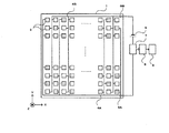
図1(A)に、第1の実施例による湾曲量検出装置の平面図を示し、図1(B)に、図1(A)の一点鎖線B1−B1における断面図を示す。ポリイミドからなる基材1の表面に、複数の凸部2が設けられている。基材1は、例えば辺の長さが4cmと3cmの長方形状である。1つの辺に平行な方向をX軸、それに直交する方向をY軸とするXYZ直交座標系を導入する。
FIG. 1A shows a plan view of the bending amount detection apparatus according to the first embodiment, and FIG. 1B shows a cross-sectional view taken along one-dot chain line B1-B1 in FIG. A plurality of
凸部2の各々は、Y軸に平行な方向に延在し、X軸に平行な一方の辺の近傍から、それに対向する辺の近傍まで至る。複数の凸部2は、X軸に平行な方向に一定のピッチで配列している。一例として、凸部2の高さは1mm、幅は1mm、相互に隣り合う凸部2の間隔も1mmである。凸部2が設けられていない領域の基材1の厚さは例えば0.5mmである。
Each of the
凸部2の表面が、アルミニウム(Al)等の導電膜3で覆われている。導電膜3の厚さは、例えば200nmである。相互に隣り合う2つの凸部2を覆う導電膜3は、相互に電気的に絶縁されている。
The surface of the
凸部2に、X軸方向の一端から他端に向かって通し番号を振ったとき、奇数番目の凸部2を覆う導電膜3が、配線4Aに接続され、偶数番目の凸部2を覆う導電膜3が、他の配線4Bに接続されている。配線4A及び4Bは、基材1の表面上に成膜されたアルミニウム等の導電膜で構成されている。配線4A及び4Bの端部に、それぞれ端子5A及び5Bが形成されている。
When serial numbers are assigned to the
端子5A及び5Bに、電源6と電流検出器7とが直列接続された電気回路が接続されている。通常の状態では、電流検出器7に電流が流れない。相互に隣り合う2つの凸部2を覆う導電膜3同士が接触すると、電流検出器7に電流が流れる。
An electric circuit in which a power source 6 and a
電流検出器7は、電流を検出すると、ドライバ回路8に電流検出信号を送信する。ドライバ回路8は、電流検出器7から電流検出信号を受信すると、警告発生器9に駆動信号を送信する。警告発生器9は、例えば発光ダイオード等の発光素子であり、駆動信号を受信すると光を発する。警告発生器9として、発音器、振動発生装置、文字表示装置等を用いてもよい。発音器は、駆動信号を受信すると、警報音を発する。振動発生装置は、駆動信号を受信すると、取扱者が認知できる振動を発生する。文字表示装置は、駆動信号を受信すると、取扱者に注意を喚起する文字情報を表示する。電源6、電流検出器7、ドライバ回路8、警告発生器9は、例えば基材1とは異なる基板上に搭載される。
When detecting the current, the
次に、図2を参照して、第1の実施例による湾曲量検出装置の製造方法について説明する。
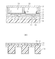
図2(A)に示すように、表面に複数の凸部2が設けられた基材1を準備する。基材1は、ポリイミドを射出成型することにより形成することができる。図2(B)に示すように、凸部2が設けられている面に、アルミニウムを真空蒸着することにより、厚さ200nmの導電膜3を形成する。図2(C)に示すように、導電膜3の表面にフォトレジストをスピンコーティングすることにより、レジスト膜Rを形成する。
Next, with reference to FIG. 2, the manufacturing method of the bending amount detection apparatus by 1st Example is demonstrated.
As shown in FIG. 2A, a
図2(D)に示すように、レジスト膜Rを露光、現像することにより、レジストパターンRPを形成する。レジストパターンRPは、凸部2の各々の側面及び上面を覆い、さらに、配線4A、4B及び端子5A、5Bが配置される領域を覆う。
As shown in FIG. 2D, the resist film R is exposed and developed to form a resist pattern RP. The resist pattern RP covers the side surfaces and the upper surface of the
図2(E)に示すように、レジストパターンRPをエッチングマスクとして導電膜3をエッチングする。図2(F)に示すように、レジストパターンRPを除去する。以上の工程により、凸部2の上面及び側面を覆う導電膜3が形成されるとともに、図1(A)に示した配線4A、4B及び端子5A、5Bが形成される。
As shown in FIG. 2E, the
図3を参照して、第1の実施例による湾曲量検出装置の動作について説明する。図3は、湾曲量検出装置を、Y軸に平行な柱面に沿うように、かつ凸部2が設けられた面が内側になるように湾曲させた状態を示す。湾曲量がある基準値に達すると、相互に隣り合う2つの凸部2aと2bとの表面を覆う導電膜3aと3bとが接触する。第1の実施例の場合には、湾曲量の基準値は、曲率半径4mmに相当する。両者が接触すると、図1(A)に示した電流検出器7に電流が流れる。これにより、警告発生器9が発光する。逆に、発光が生じていないときには、湾曲量が基準値に達していないことを意味する。このように、凸部2、導電膜3、配線4A、4B、電源6、及び電流検出器7が、湾曲量検出手段を構成する。
With reference to FIG. 3, the operation of the bending amount detection apparatus according to the first embodiment will be described. FIG. 3 shows a state in which the bending amount detection device is bent along a column surface parallel to the Y axis so that the surface on which the
取扱者は、この発光等の警告が発せられることにより、湾曲量が基準値に達したことを容易に認知することができる。これにより、さらなる湾曲の発生を防止することができる。この湾曲量検出装置を、フレキシブル液晶表示装置、ペーパライクディスプレイ、可撓性照明パネル等の可撓性機能パネルに貼り付けることにより、可撓性機能パネルの変形量が許容限度に近づいたことを、取扱者に認知させることができる。 The operator can easily recognize that the bending amount has reached the reference value by issuing a warning such as light emission. Thereby, generation | occurrence | production of the further curve can be prevented. By attaching this bending amount detection device to a flexible functional panel such as a flexible liquid crystal display device, a paper-like display, or a flexible lighting panel, the deformation amount of the flexible functional panel is close to the allowable limit. , You can make the handlers recognize.
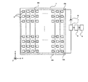
図4に、第2の実施例による湾曲量検出装置の平面図を示す。以下、図1(A)に示した第1の実施例による湾曲量検出装置との相違点に着目して説明する。
第1の実施例では、Y軸方向に長い凸部2がX軸方向に等間隔で配列していたが、第2の実施例では、複数の凸部2が行列状に、X軸方向及びY軸方向に等間隔で配置されている。凸部2の各々の上面及び側面は、第1の実施例の場合と同様に導電膜3で覆われている。X軸に平行な並びを行、Y軸に平行な並びを列としたとき、行番号と列番号との組み合わせで1つの凸部2を特定することができる。
FIG. 4 shows a plan view of a bending amount detection apparatus according to the second embodiment. Hereinafter, the description will be given focusing on differences from the bending amount detection apparatus according to the first embodiment shown in FIG.
In the first embodiment, the
行番号と列番号との和が偶数になる凸部2(図4においてハッチが付された凸部)を覆う導電膜は、配線4Aに接続され、行番号と列番号との和が奇数になる凸部2(図4において白抜きの凸部)を覆う導電膜は、もう一方の配線4Bに接続されている。すなわち、X軸方向及びY軸方向に隣り合う凸部2を覆う導電膜に、相互に逆極性の電圧が印加されている。その他の構成は、第1の実施例による湾曲量検出装置の構成と同様である。
The conductive film covering the convex part 2 (the convex part hatched in FIG. 4) in which the sum of the row number and the column number is an even number is connected to the
第1の実施例の場合には、基材1が、X軸に平行な柱面に沿うように湾曲し易く、Y軸に平行な柱面に沿うようには湾曲しにくかった。第2の実施例の場合には、いずれの方向にも同等に湾曲する。さらに、いずれの方向に湾曲した場合であっても、湾曲量が基準値に達したとき、発光等により警告を発することができる。
In the case of the first example, the
図5に、第3の実施例による湾曲量検出装置の平面図を示す。図4に示した第2の実施例では、凸部2がX軸方向及びY軸方向に等間隔で配置されていたが、第3の実施例では、Y軸方向の間隔がX軸方向の間隔よりも広くされている。その他の構成は、第2の実施例による湾曲量検出装置の構成と同様である。
FIG. 5 shows a plan view of a bending amount detection apparatus according to the third embodiment. In the second embodiment shown in FIG. 4, the
第3の実施例では、Y軸に平行な柱面に沿うように湾曲したときの湾曲量の基準値が、X軸に平行な柱面に沿うように湾曲したときの湾曲量の基準値よりも大きい。このため、Y軸に平行な柱面に沿うように湾曲したときに、X軸に平行な柱面に沿うように湾曲した場合に比べて、湾曲量がより小さい時点で、発光等の警告が発せられる。 In the third embodiment, the reference value of the amount of curvature when curved along the column surface parallel to the Y axis is greater than the reference value of the amount of curvature when curved along the column surface parallel to the X axis. Is also big. For this reason, when it is curved along a column surface parallel to the Y-axis, a warning such as light emission is issued at a time when the amount of bending is smaller than when it is curved along a column surface parallel to the X-axis. Be emitted.
例えば、インジウム錫酸化物(ITO)等の透明導電膜からなる配線が、第1の方向に平行に配置され、アルミニウム等の金属配線が、それに直交する第2の方向に平行に配置された可撓性機能パネルに、第3の実施例による湾曲量検出装置を取り付ける場合について説明する。ITO等からなる配線は、金属配線に比べて変形による損傷を受け易い。第3の実施例による湾曲量検出装置のX軸方向が、ITO等からなる配線の延在する第1の方向と平行になるように、湾曲量検出装置を可撓性機能パネルに貼り付ける。 For example, a wiring made of a transparent conductive film such as indium tin oxide (ITO) is arranged in parallel to the first direction, and a metal wiring such as aluminum is arranged in parallel to a second direction orthogonal thereto. A case where the bending amount detection device according to the third embodiment is attached to the flexible function panel will be described. Wiring made of ITO or the like is more susceptible to damage due to deformation than metal wiring. The bending amount detection device is attached to the flexible function panel so that the X-axis direction of the bending amount detection device according to the third embodiment is parallel to the first direction in which the wiring made of ITO or the like extends.
これにより、ITO等からなる配線が変形する方向に湾曲する場合には、湾曲量が比較的小さい時点で警告を発し、金属配線が変形する方向へは、比較的大きな湾曲を許容することができる。 As a result, when the wiring made of ITO or the like curves in the direction of deformation, a warning is issued when the amount of bending is relatively small, and a relatively large curve can be allowed in the direction of deformation of the metal wiring. .
上記第1〜第3の実施例では、隣り合う凸部を覆う導電膜が接触することにより、湾曲量を検出したが、その他の方法で湾曲量を検出することも可能である。例えば、湾曲することによって電気抵抗が変化する歪ゲージを、可撓性基材に貼り付けてもよい。電気抵抗の変化を検出することにより、湾曲量に関する情報を得ることができる。 In the first to third embodiments, the bending amount is detected by contact of the conductive film covering the adjacent convex portions. However, the bending amount can be detected by other methods. For example, a strain gauge whose electrical resistance changes by bending may be attached to the flexible substrate. Information relating to the amount of bending can be obtained by detecting a change in electrical resistance.
次に、図6(A)及び図6(B)を参照して、第4の実施例による可撓性画像表示装置について説明する。第4の実施例による可撓性画像表示装置は、可撓性を有する画像表示板、例えば電気泳動を利用したペーパライクディスプレイに、第1、第2、または第3の実施例による可撓性基材を適用したものである。 Next, with reference to FIGS. 6A and 6B, a flexible image display apparatus according to a fourth embodiment will be described. The flexible image display apparatus according to the fourth embodiment is a flexible image display board, for example, a paper-like display using electrophoresis, and the flexibility according to the first, second, or third embodiment. A substrate is applied.
図6(A)に、第4の実施例による可撓性画像表示装置の2つの画素部分の断面図を示し、図6(B)に、多数の画素部分の断面図を示す。後方基板11の表面上に、画素ごとに薄膜トランジスタ等のスイッチング素子13が形成されている。スイッチング素子13を覆うように、後方基板11の上に層間絶縁膜15が形成されている。層間絶縁膜15の上に、画素ごとに第1電極14が形成されている。第1電極14は、層間絶縁膜15を貫通するビアホール内を経由して、対応するスイッチング素子13に接続されている。第1電極14を覆うように、窒化シリコン等からなる無機絶縁膜16が形成されている。
FIG. 6A shows a cross-sectional view of two pixel portions of the flexible image display device according to the fourth embodiment, and FIG. 6B shows a cross-sectional view of many pixel portions. A switching
絶縁膜16から間隙を隔てて表示側基板10が配置されている。表示側基板10と絶縁膜16との間に隔壁12が設けられている。隔壁12は、絶縁膜16の表面内に格子状に配置されており、画素を画定するとともに、表示側基板10と絶縁膜16との間に一定の間隙を確保する。
The display-
隔壁12と絶縁膜16との間にアルミニウム等からなる第2電極17が配置されている。第2電極17は、例えば、隔壁12の内部に埋め込まれていてもよい。絶縁膜16、表示側基板10、及び隔壁12に囲まれた空間内にシリコンオイル等の絶縁性液体20が充填されている。絶縁性液体20内に、粒径1〜2μm程度の多数の帯電泳動粒子21が分散されている。帯電泳動粒子21の材料の例として、カーボンブラックを含有したポリスチレン−ポリメチルメタクリレート共重合体樹脂等が挙げられる。
A
後方基板11と表示側基板10とで挟まれたペーパライクディスプレイが構成される。このペーパライクディスプレイは、例えば特開2003−161966号公報に開示されている。
A paper-like display sandwiched between the
後方基板11の外側の表面上に、湾曲量検出装置30が貼り付けられている。湾曲量検出装置30は、上述の第1〜第3の実施例のいずれかによる湾曲量検出装置と同一のものである。面内方向に関して、湾曲量検出装置30の一つの凸部内に、複数の画素が配置されている。
On the outer surface of the
第4の実施例による可撓性画像表示装置の動作について説明する。第2電極17は接地されている。帯電泳動粒子21が正に帯電しているとする。第1電極14に正の電圧を印加すると、図6(A)の右側の画素に示すように、帯電泳動粒子21は、第2電極17の近傍に集まる。第1電極14の表面を白色にしておくと、この画素は白表示状態になる。第1電極14に負の電圧を印加すると、図6(A)の左側の画素に示すように、帯電泳動粒子21が第1電極16上に広がる。これにより、この画素は、帯電泳動粒子21の黒色が観測される状態になる。
The operation of the flexible image display device according to the fourth embodiment will be described. The
後方基板11が内側になるように、可撓性画像表示装置を湾曲させ、その湾曲量が基準値に達すると、湾曲量検出装置30が警告を発する。取扱者が警告を認知し、それ以上の湾曲の発生を抑制することにより、ペーパライクディスプレイの破壊を防止することができる。
When the flexible image display device is bent so that the
図7に、第4の実施例の変形例による可撓性画像表示装置の分解斜視図を示す。ペーパライクディスプレイ35に、画像を表示する画像表示領域35Aと、画像表示領域35Aを取り囲む額縁領域35Bとが画定されている。額縁領域35Bが枠36に接着されている。画像表示領域35Aは、枠36に重ならない。このため、枠36に遮られることなく画像表示領域35Aを視認することができる。
FIG. 7 is an exploded perspective view of a flexible image display device according to a modification of the fourth embodiment. On the paper-
枠36の片面または両面に、第1〜第3の実施例による湾曲量検出装置のいずれかと同様の湾曲量検出装置が接着されている。ペーパライクディスプレイ35を湾曲させると、枠36もそれに応じて変形する。枠36の変形量が基準値に達すると警告が発せられため、ペーパライクディスプレイ35の破壊を防止することができる。
A curvature amount detection device similar to any one of the curvature amount detection devices according to the first to third embodiments is bonded to one surface or both surfaces of the
枠36自体を、湾曲量検出装置で構成してもよい。また、枠36の両面に湾曲量検出装置を貼り付けてもよい。両面に貼り付けると、いずれの面が内側になるように湾曲した場合であっても、警告を発することができる。
The
図8に示すように、額縁領域35Bに直接凸部35Cを設けてもよい。この凸部35Cの表面を導電膜で覆い、第1〜第3の実施例による湾曲量検出装置を構成することができる。例えば、額縁領域35Bは、画像表示領域35Aの4つの辺に沿った4つの領域に区分される。この4つの領域の各々に、その幅方向に延在する凸部35Cが形成される。画像表示領域35Aに凸部35Cが配置されないため、湾曲量検出装置に遮られること無く、両面から画像を視認することが可能になる。
As shown in FIG. 8, a convex portion 35C may be provided directly in the
なお、ペーパライクディスプレイとは、紙のように薄いディスプレイの総称であり、第4の実施例による可撓性画像表示装置のように、帯電した粒子を水平方向(面内方向)に移動させる水平移動型電気泳動ディスプレイの他に、種々の方式が提案されている。例えば、マイクロカプセル型電気泳動ディスプレイ、ツイスティングボールディスプレイ、電界析出・溶解式ディスプレイ等が提案されている。第1〜第3の実施例による湾曲量検出装置は、これら種々のペーパライクディスプレイにも適用することが可能である。 The paper-like display is a generic name for thin displays such as paper, and as in the flexible image display device according to the fourth embodiment, the horizontal direction in which charged particles are moved in the horizontal direction (in-plane direction). In addition to the mobile electrophoretic display, various methods have been proposed. For example, a microcapsule type electrophoretic display, a twisting ball display, a field deposition / dissolution display, and the like have been proposed. The bending amount detection devices according to the first to third embodiments can be applied to these various paper-like displays.
次に、図9(A)及び図9(B)を参照して、第5の実施例による可撓性画像表示装置について説明する。第5の実施例による可撓性画像表示装置は、有機EL素子に、第1〜第3の実施例による湾曲量検出装置を適用したものである。 Next, a flexible image display device according to a fifth embodiment will be described with reference to FIGS. The flexible image display device according to the fifth embodiment is obtained by applying the bending amount detection device according to the first to third embodiments to an organic EL element.
図9(A)に、第5の実施例による可撓性画像表示装置の3つの画素部分の断面図を示し、図9(B)に、多数の画素部分の断面図を示す。可撓性を有する透明フィルム40の表面上に、ITOからなる複数の正極41が形成されている。正極41は、透明フィルム40の表面内において、相互に平行(図9(A)において横方向)に配置されている。
FIG. 9A shows a cross-sectional view of three pixel portions of the flexible image display device according to the fifth embodiment, and FIG. 9B shows a cross-sectional view of many pixel portions. A plurality of
透明フィルム40の上に、正極41と交差するように、複数の帯状の有機発光層42が配置されている。有機発光層42の各々は、透明フィルム40側から順番に、正孔輸送層42A、発光層42B、及び電子輸送層42Cが積層された多層構造を有する。電子輸送層42Cの表面上に、アルミニウム等の負極45が形成されている。なお、必要に応じて、正極41と正孔輸送層42Aとの間に正孔注入層を挿入してもよい。また、負極45と電子輸送層42Cとの間に電子注入層を挿入してもよい。正極41と有機発光層42との交差箇所が画素として機能する。
A plurality of strip-shaped organic
透明フィルム41から負極45までの構成は、例えば特開2003−272864号公報に開示されている。
エポキシ樹脂系接着剤48を用いて湾曲量検出装置50を透明フィルム40に貼り合わせることにより、正極41、有機発光層42、及び負極45が封止されている。湾曲量検出装置50は、上述の第1〜第3の実施例による湾曲量検出装置のいずれかと同一のものであり、凸部の付された表面が外側を向くように貼り合わせられている。
The structure from the
The
発光層42Bで発生した光は、透明フィルム40を通過して外部に放射される。湾曲量検出装置50が内側になるように、可撓性画像表示装置を湾曲させ、その湾曲量が基準値に達すると、湾曲量検出装置50により警告が発せられる。取扱者が、警告を認知し、それ以上の湾曲の発生を抑制することにより、有機EL素子の破壊を防止することができる。
The light generated in the
第5の実施例においても、図7に示したように、有機EL素子に取り付けた枠に、湾曲量検出装置を貼り付けてもよいし、図8に示したように、額縁領域にのみ凸部を設け、湾曲量検出装置を形成してもよい。 Also in the fifth embodiment, as shown in FIG. 7, the bending amount detection device may be attached to the frame attached to the organic EL element, or as shown in FIG. A bending amount detection device may be formed by providing a portion.
次に、図10(A)及び図10(B)を参照して、第6の実施例による可撓性画像表示装置について説明する。第6の実施例による可撓性画像表示装置は、可撓性を有する液晶表示素子に、第1〜第3の実施例による湾曲量検出装置のいずれかを適用したものである。 Next, a flexible image display device according to a sixth embodiment will be described with reference to FIGS. In the flexible image display device according to the sixth embodiment, any one of the bending amount detection devices according to the first to third embodiments is applied to a liquid crystal display element having flexibility.
図10(A)に、第6の実施例による可撓性画像表示装置の両端近傍の断面図を示し、図10(B)に、多数の画素部分の断面図を示す。厚さ100μm程度の可撓性を有する一対の基板60及び65が、間隙を隔てて平行に配置されている。基板60及び65の内側の表面に、それぞれITO等からなる透明電極61及び66が形成されている。基板60及び65は、一般にPET、PC、PES等をベースとし、ガスバリア層、表面処理層等が積層された構造を有する。透明電極61は、図の横方向に延在する複数の帯状の電極で構成され、透明電極66は、図の紙面に垂直な方向に延在する複数の帯状の電極で構成される。両者の交差する箇所に画素が画定される。透明電極61及び66を覆うように、基板60及び65の上に、それぞれ配向膜62及び67が形成されている。
FIG. 10A shows a cross-sectional view of the vicinity of both ends of the flexible image display device according to the sixth embodiment, and FIG. 10B shows a cross-sectional view of a large number of pixel portions. A pair of
2枚の基板60及び65の間に、間隙保持部材70及びネマチック液晶71が充填されている。シール剤72により、基板60と65とが重合接着されている。なお、必要に応じて、カラーフィルタや偏光フィルムが配置される。この液晶表示素子は、例えば特開平9−101509号公報に開示されている。
A
一方の基板60の外側の表面に、湾曲量検出装置75が貼り付けられている。湾曲量検出装置75は、上述の第1〜第3の実施例による湾曲量検出装置のいずれかと同一のものである。湾曲量検出装置75の凸部を付された面が、外側を向く。
A curvature
湾曲量検出装置75が内側になるように湾曲させた場合、湾曲量が基準値に達すると、湾曲量検出装置75により警告が発せられる。このため、それ以上の湾曲の発生を抑制し、液晶表示素子の破壊を防止することができる。
When the bending
第6の実施例においても、図7に示した構造と同様に、液晶表示素子に取り付けた枠に、湾曲量検出装置を貼り付けてもよいし、図8に示した構造と同様に、額縁領域にのみ凸部を設け、湾曲量検出装置を形成してもよい。 Also in the sixth embodiment, similarly to the structure shown in FIG. 7, the bending amount detection device may be attached to the frame attached to the liquid crystal display element, or the frame is similar to the structure shown in FIG. 8. A convex amount may be provided only in the region to form a bending amount detection device.
上記第4〜第6の実施例による可撓性画像表示装置においては、画像表示板、例えばペーパライクディスプレイ、有機EL素子、液晶表示素子等を過度に変形させると、不可逆的な劣化が生じる。「不可逆的な劣化」とは、画像表示板を元の形状に戻しても、表示品質が元に戻らないような劣化を意味する。不可逆的な劣化の例として、例えば、ITO等の電極の割れ、可撓性フィルムの白濁等が挙げられる。 In the flexible image display devices according to the fourth to sixth embodiments, irreversible degradation occurs when an image display plate, such as a paper-like display, an organic EL element, a liquid crystal display element, or the like is excessively deformed. The “irreversible deterioration” means deterioration that does not return the display quality even if the image display board is returned to its original shape. Examples of irreversible deterioration include cracks in electrodes such as ITO, and cloudiness of flexible films.
このような不可逆的な劣化を生じさせる変形が発生する前に、湾曲量検出装置が警告を発するように、湾曲量の基準値を設定することが好ましい。湾曲量の基準値は、凸部の幾何学的形状、高さ、間隔等を調節することにより、所望の値に設定することができる。 It is preferable to set the bending amount reference value so that the bending amount detecting device issues a warning before the deformation that causes such irreversible deterioration occurs. The reference value of the amount of bending can be set to a desired value by adjusting the geometric shape, height, interval, etc. of the protrusions.
以上実施例に沿って本発明を説明したが、本発明はこれらに制限されるものではない。例えば、種々の変更、改良、組み合わせ等が可能なことは当業者に自明であろう。 Although the present invention has been described with reference to the embodiments, the present invention is not limited thereto. It will be apparent to those skilled in the art that various modifications, improvements, combinations, and the like can be made.
1 基材
2 凸部
3 導電膜
4A、4B 配線
5A、5B 端子
6 電源
7 電流検出器
8 ドライバ回路
9 警告発生器
10 表示側基板
11 後方基板
12 隔壁
13 スイッチング素子
14 第1電極
15 層間絶縁膜
16 無機絶縁膜
17 第2電極
20 絶縁性液体
21 帯電泳動粒子
30、50、75 湾曲量検出装置
35 ペーパライクディスプレイ
35A 画像表示領域
35B 額縁領域
35C 凸部
36 枠
40 透明フィルム
41 正極
42 有機発光層
45 負極
48 接着剤
60、65 基板
61、66 透明電極
62、67 配向膜
70 間隙保持部材
71 液晶
72 シール剤
DESCRIPTION OF
Claims (5)
前記基材の湾曲量が、ある基準値に達したか否かを検出する湾曲量検出手段と、
前記湾曲量検出手段により、前記基材の湾曲量が前記基準値に達したことが検出されると、湾曲量が基準値に達したことを通知する警告発生手段と
を有する湾曲量検出装置。 A flexible substrate;
A bending amount detecting means for detecting whether or not the bending amount of the base material has reached a certain reference value;
A bending amount detection apparatus comprising: a warning generation unit that notifies that the bending amount has reached the reference value when the bending amount detection unit detects that the bending amount of the base material has reached the reference value.
前記湾曲量検出手段は、前記基材の凸部の各々の表面の少なくとも一部を覆う導電膜と、前記凸部のうち相互に隣り合う2つの凸部の表面を覆う導電膜に、相互に反対の極性の電圧が印加されるように、前記導電膜に電圧を印加する電圧印加手段と、相互に隣り合う2つの凸部の表面を覆う導電膜が接触して両者の間に電流が流れると、その電流を検出する電流検出手段とを含む請求項1に記載の湾曲量検出装置。 A plurality of convex portions are provided on the surface of the base material,
The bending amount detection means includes a conductive film that covers at least a part of each surface of the convex portions of the base material, and a conductive film that covers the surfaces of two convex portions adjacent to each other among the convex portions. The voltage application means for applying a voltage to the conductive film and the conductive film covering the surfaces of the two adjacent protrusions are in contact with each other so that a voltage having the opposite polarity is applied, and a current flows between them. The bending amount detection device according to claim 1, further comprising: current detection means for detecting the current.
前記機能性パネルに取り付けられた請求項1〜3のいずれかに記載の湾曲量検出装置とを有し、
前記湾曲量検出装置は、前記機能性パネルの湾曲に追随して湾曲する可撓性装置。 A functional panel having flexibility and displaying an image or emitting illumination light;
The bending amount detection device according to any one of claims 1 to 3 attached to the functional panel,
The bending amount detection device is a flexible device that bends following the bending of the functional panel.
Priority Applications (1)
| Application Number | Priority Date | Filing Date | Title |
|---|---|---|---|
| JP2005149728A JP4749764B2 (en) | 2005-05-23 | 2005-05-23 | Curvature detection device and flexible device |
Applications Claiming Priority (1)
| Application Number | Priority Date | Filing Date | Title |
|---|---|---|---|
| JP2005149728A JP4749764B2 (en) | 2005-05-23 | 2005-05-23 | Curvature detection device and flexible device |
Publications (2)
| Publication Number | Publication Date |
|---|---|
| JP2006330082A true JP2006330082A (en) | 2006-12-07 |
| JP4749764B2 JP4749764B2 (en) | 2011-08-17 |
Family
ID=37551865
Family Applications (1)
| Application Number | Title | Priority Date | Filing Date |
|---|---|---|---|
| JP2005149728A Expired - Fee Related JP4749764B2 (en) | 2005-05-23 | 2005-05-23 | Curvature detection device and flexible device |
Country Status (1)
| Country | Link |
|---|---|
| JP (1) | JP4749764B2 (en) |
Cited By (12)
| Publication number | Priority date | Publication date | Assignee | Title |
|---|---|---|---|---|
| JP2009109337A (en) * | 2007-10-30 | 2009-05-21 | Minebea Co Ltd | Bend sensor |
| WO2011155117A1 (en) * | 2010-06-09 | 2011-12-15 | シャープ株式会社 | Display device |
| KR20130057029A (en) * | 2011-11-23 | 2013-05-31 | 삼성전자주식회사 | Display device and control method thereof |
| WO2014010329A1 (en) * | 2012-07-09 | 2014-01-16 | ソニー株式会社 | Display device, and electronic equipment |
| KR20140139263A (en) * | 2013-05-27 | 2014-12-05 | 삼성디스플레이 주식회사 | Flexable display device having guide function of gesture command and method thereof |
| CN104318861A (en) * | 2014-09-24 | 2015-01-28 | 京东方科技集团股份有限公司 | Flexible screen, bending identification method of flexible screen, and flexible display device |
| KR20150035232A (en) * | 2013-09-27 | 2015-04-06 | 삼성전자주식회사 | Wearable device |
| JP2015228022A (en) * | 2014-05-06 | 2015-12-17 | 株式会社半導体エネルギー研究所 | Electronic device |
| WO2016043215A1 (en) * | 2014-09-19 | 2016-03-24 | 日本電気株式会社 | Device for preventing deformation of display device, deformation prevention method, and deformation prevention program |
| US9805494B2 (en) | 2012-05-11 | 2017-10-31 | Semiconductor Energy Laboratory Co., Ltd. | Electronic device, storage medium, program, and displaying method |
| US9851756B2 (en) | 2015-03-19 | 2017-12-26 | International Business Machines Corporation | Recommending bending lines on flexible displays |
| JP2018032409A (en) * | 2012-05-31 | 2018-03-01 | 株式会社半導体エネルギー研究所 | Electronic apparatus |
Citations (3)
| Publication number | Priority date | Publication date | Assignee | Title |
|---|---|---|---|---|
| JPH0587511A (en) * | 1991-07-24 | 1993-04-06 | Yamaha Corp | Bending detection device |
| JP2001074569A (en) * | 1999-09-02 | 2001-03-23 | Tokin Corp | Planar capacitance type twist strain sensor |
| JP2002278515A (en) * | 2001-03-15 | 2002-09-27 | Minolta Co Ltd | Image display device |
-
2005
- 2005-05-23 JP JP2005149728A patent/JP4749764B2/en not_active Expired - Fee Related
Patent Citations (3)
| Publication number | Priority date | Publication date | Assignee | Title |
|---|---|---|---|---|
| JPH0587511A (en) * | 1991-07-24 | 1993-04-06 | Yamaha Corp | Bending detection device |
| JP2001074569A (en) * | 1999-09-02 | 2001-03-23 | Tokin Corp | Planar capacitance type twist strain sensor |
| JP2002278515A (en) * | 2001-03-15 | 2002-09-27 | Minolta Co Ltd | Image display device |
Cited By (37)
| Publication number | Priority date | Publication date | Assignee | Title |
|---|---|---|---|---|
| JP2009109337A (en) * | 2007-10-30 | 2009-05-21 | Minebea Co Ltd | Bend sensor |
| US9213195B2 (en) | 2010-06-09 | 2015-12-15 | Sharp Kabushiki Kaisha | Display device |
| WO2011155117A1 (en) * | 2010-06-09 | 2011-12-15 | シャープ株式会社 | Display device |
| KR20130057029A (en) * | 2011-11-23 | 2013-05-31 | 삼성전자주식회사 | Display device and control method thereof |
| KR101879615B1 (en) * | 2011-11-23 | 2018-07-19 | 삼성전자주식회사 | Display device and control method thereof |
| US10719972B2 (en) | 2012-05-11 | 2020-07-21 | Semiconductor Energy Laboratory Co., Ltd. | Electronic device, storage medium, program, and displaying method |
| US20190172248A1 (en) | 2012-05-11 | 2019-06-06 | Semiconductor Energy Laboratory Co., Ltd. | Electronic device, storage medium, program, and displaying method |
| US11815956B2 (en) | 2012-05-11 | 2023-11-14 | Semiconductor Energy Laboratory Co., Ltd. | Electronic device, storage medium, program, and displaying method |
| US11216041B2 (en) | 2012-05-11 | 2022-01-04 | Semiconductor Energy Laboratory Co., Ltd. | Electronic device, storage medium, program, and displaying method |
| US10467797B2 (en) | 2012-05-11 | 2019-11-05 | Semiconductor Energy Laboratory Co., Ltd. | Electronic device, storage medium, program, and displaying method |
| US10380783B2 (en) | 2012-05-11 | 2019-08-13 | Semiconductor Energy Laboratory Co., Ltd. | Electronic device, storage medium, program, and displaying method |
| US9805494B2 (en) | 2012-05-11 | 2017-10-31 | Semiconductor Energy Laboratory Co., Ltd. | Electronic device, storage medium, program, and displaying method |
| JP2018032409A (en) * | 2012-05-31 | 2018-03-01 | 株式会社半導体エネルギー研究所 | Electronic apparatus |
| JP2020060779A (en) * | 2012-05-31 | 2020-04-16 | 株式会社半導体エネルギー研究所 | Electronic apparatus |
| JP2021185433A (en) * | 2012-05-31 | 2021-12-09 | 株式会社半導体エネルギー研究所 | Electronic apparatus |
| US9854667B2 (en) | 2012-07-09 | 2017-12-26 | Sony Corporation | Display unit and electronic apparatus |
| US11343908B2 (en) | 2012-07-09 | 2022-05-24 | Sony Corporation | Display unit and electronic apparatus |
| US10674602B2 (en) | 2012-07-09 | 2020-06-02 | Sony Corporation | Display unit and electronic apparatus |
| US10219370B2 (en) | 2012-07-09 | 2019-02-26 | Sony Corporation | Display unit and electronic apparatus |
| US11696394B2 (en) | 2012-07-09 | 2023-07-04 | Interdigital Ce Patent Holdings, Sas | Display unit and electronic apparatus |
| WO2014010329A1 (en) * | 2012-07-09 | 2014-01-16 | ソニー株式会社 | Display device, and electronic equipment |
| JPWO2014010329A1 (en) * | 2012-07-09 | 2016-06-20 | ソニー株式会社 | Display device and electronic device |
| KR20140139263A (en) * | 2013-05-27 | 2014-12-05 | 삼성디스플레이 주식회사 | Flexable display device having guide function of gesture command and method thereof |
| KR102145568B1 (en) * | 2013-05-27 | 2020-08-31 | 삼성디스플레이 주식회사 | Flexable display device having guide function of gesture command and method thereof |
| KR20150035232A (en) * | 2013-09-27 | 2015-04-06 | 삼성전자주식회사 | Wearable device |
| KR102014445B1 (en) | 2013-09-27 | 2019-08-29 | 삼성전자주식회사 | Wearable device |
| US10606379B2 (en) | 2014-05-06 | 2020-03-31 | Semiconductor Energy Laboratory Co., Ltd. | Electronic device |
| KR20170005019A (en) * | 2014-05-06 | 2017-01-11 | 가부시키가이샤 한도오따이 에네루기 켄큐쇼 | Electronic device |
| JP2015228022A (en) * | 2014-05-06 | 2015-12-17 | 株式会社半導体エネルギー研究所 | Electronic device |
| US11216106B2 (en) | 2014-05-06 | 2022-01-04 | Semiconductor Energy Laboratory Co., Ltd. | Electronic device |
| KR102495922B1 (en) | 2014-05-06 | 2023-02-02 | 가부시키가이샤 한도오따이 에네루기 켄큐쇼 | Electronic device |
| US11740728B2 (en) | 2014-05-06 | 2023-08-29 | Semiconductor Energy Laboratory Co., Ltd. | Electronic device |
| WO2016043215A1 (en) * | 2014-09-19 | 2016-03-24 | 日本電気株式会社 | Device for preventing deformation of display device, deformation prevention method, and deformation prevention program |
| WO2016045243A1 (en) * | 2014-09-24 | 2016-03-31 | 京东方科技集团股份有限公司 | Flexible screen and bending identification method therefor and flexible display apparatus |
| US9881977B2 (en) | 2014-09-24 | 2018-01-30 | Boe Technology Group Co., Ltd. | Flexible screen and bend identifying method thereof, flexible display apparatus |
| CN104318861A (en) * | 2014-09-24 | 2015-01-28 | 京东方科技集团股份有限公司 | Flexible screen, bending identification method of flexible screen, and flexible display device |
| US9851756B2 (en) | 2015-03-19 | 2017-12-26 | International Business Machines Corporation | Recommending bending lines on flexible displays |
Also Published As
| Publication number | Publication date |
|---|---|
| JP4749764B2 (en) | 2011-08-17 |
Similar Documents
| Publication | Publication Date | Title |
|---|---|---|
| JP4749764B2 (en) | Curvature detection device and flexible device | |
| JP4777338B2 (en) | Flexible base material for suppressing plastic deformation and flexible image display device | |
| KR102634958B1 (en) | Flexible display device with wire having reinforced portion and manufacturing method for the same | |
| KR101908501B1 (en) | Integrated Touch Screen With Organic Emitting Display Device and Method for Manufacturing the Same | |
| CN106716642B (en) | Display device having divided wiring patterns | |
| CN107978625B (en) | Flexible display device | |
| JP5676554B2 (en) | Organic light emitting display | |
| JP2006048006A (en) | Liquid crystal display device and manufacturing method thereof | |
| JP6607762B2 (en) | Display device | |
| JP2006349788A (en) | Electrooptical apparatus, manufacturing method for the same and electronic equipment | |
| JP2009237280A (en) | Display device | |
| JP2019012098A (en) | Display device | |
| CN111625113A (en) | Active matrix substrate, liquid crystal display device and embedded touch panel | |
| CN111564568A (en) | Display panel and display device | |
| KR102611213B1 (en) | Display device | |
| KR102555404B1 (en) | Flexible Display and Method for Manufacturing the Same | |
| JP7473567B2 (en) | Touch electrode structure and manufacturing method thereof, touch panel and electronic device | |
| JP2018112842A (en) | Touch panel sensor and display with touch position detection function | |
| WO2019138849A1 (en) | Display device | |
| KR101298278B1 (en) | Signal wire and display substrate having the signal wire | |
| KR20230161290A (en) | Display device and method for manufacturing the display device | |
| JP2007212610A (en) | Liquid crystal display device, liquid crystal display panel, and method for manufacturing liquid crystal display device | |
| CN117241623A (en) | Display panel and display device | |
| WO2019102845A1 (en) | Display device | |
| KR100894044B1 (en) | Liquid crystal display |
Legal Events
| Date | Code | Title | Description |
|---|---|---|---|
| A711 | Notification of change in applicant |
Free format text: JAPANESE INTERMEDIATE CODE: A712 Effective date: 20070201 |
|
| A621 | Written request for application examination |
Free format text: JAPANESE INTERMEDIATE CODE: A621 Effective date: 20080124 |
|
| A977 | Report on retrieval |
Free format text: JAPANESE INTERMEDIATE CODE: A971007 Effective date: 20110204 |
|
| A131 | Notification of reasons for refusal |
Free format text: JAPANESE INTERMEDIATE CODE: A131 Effective date: 20110215 |
|
| A521 | Written amendment |
Free format text: JAPANESE INTERMEDIATE CODE: A523 Effective date: 20110406 |
|
| TRDD | Decision of grant or rejection written | ||
| A01 | Written decision to grant a patent or to grant a registration (utility model) |
Free format text: JAPANESE INTERMEDIATE CODE: A01 Effective date: 20110426 |
|
| A61 | First payment of annual fees (during grant procedure) |
Free format text: JAPANESE INTERMEDIATE CODE: A61 Effective date: 20110518 |
|
| R150 | Certificate of patent or registration of utility model |
Ref document number: 4749764 Country of ref document: JP Free format text: JAPANESE INTERMEDIATE CODE: R150 Free format text: JAPANESE INTERMEDIATE CODE: R150 |
|
| FPAY | Renewal fee payment (event date is renewal date of database) |
Free format text: PAYMENT UNTIL: 20140527 Year of fee payment: 3 |
|
| R250 | Receipt of annual fees |
Free format text: JAPANESE INTERMEDIATE CODE: R250 |
|
| R250 | Receipt of annual fees |
Free format text: JAPANESE INTERMEDIATE CODE: R250 |
|
| R250 | Receipt of annual fees |
Free format text: JAPANESE INTERMEDIATE CODE: R250 |
|
| R250 | Receipt of annual fees |
Free format text: JAPANESE INTERMEDIATE CODE: R250 |
|
| R250 | Receipt of annual fees |
Free format text: JAPANESE INTERMEDIATE CODE: R250 |
|
| LAPS | Cancellation because of no payment of annual fees |