JP2006309226A - Display panel, display device having the same and method of driving the same - Google Patents
Display panel, display device having the same and method of driving the same Download PDFInfo
- Publication number
- JP2006309226A JP2006309226A JP2006118201A JP2006118201A JP2006309226A JP 2006309226 A JP2006309226 A JP 2006309226A JP 2006118201 A JP2006118201 A JP 2006118201A JP 2006118201 A JP2006118201 A JP 2006118201A JP 2006309226 A JP2006309226 A JP 2006309226A
- Authority
- JP
- Japan
- Prior art keywords
- impulse
- gate
- voltage
- data
- liquid crystal
- Prior art date
- Legal status (The legal status is an assumption and is not a legal conclusion. Google has not performed a legal analysis and makes no representation as to the accuracy of the status listed.)
- Withdrawn
Links
- 238000000034 method Methods 0.000 title claims abstract description 22
- 239000004973 liquid crystal related substance Substances 0.000 claims abstract description 80
- 239000003990 capacitor Substances 0.000 claims abstract description 79
- 230000003213 activating effect Effects 0.000 claims abstract 3
- 238000005401 electroluminescence Methods 0.000 claims description 9
- 230000003111 delayed effect Effects 0.000 claims description 7
- 239000010409 thin film Substances 0.000 claims description 4
- 238000010586 diagram Methods 0.000 description 22
- 101000805729 Homo sapiens V-type proton ATPase 116 kDa subunit a 1 Proteins 0.000 description 17
- 101000854879 Homo sapiens V-type proton ATPase 116 kDa subunit a 2 Proteins 0.000 description 17
- 101000854873 Homo sapiens V-type proton ATPase 116 kDa subunit a 4 Proteins 0.000 description 17
- 102100020737 V-type proton ATPase 116 kDa subunit a 4 Human genes 0.000 description 17
- 101100214488 Solanum lycopersicum TFT2 gene Proteins 0.000 description 16
- 101100489584 Solanum lycopersicum TFT1 gene Proteins 0.000 description 13
- 238000009616 inductively coupled plasma Methods 0.000 description 12
- 235000010384 tocopherol Nutrition 0.000 description 12
- 235000019731 tricalcium phosphate Nutrition 0.000 description 12
- 230000002093 peripheral effect Effects 0.000 description 9
- 239000000758 substrate Substances 0.000 description 9
- 238000002834 transmittance Methods 0.000 description 6
- 102100029361 Aromatase Human genes 0.000 description 2
- 101000919395 Homo sapiens Aromatase Proteins 0.000 description 2
- 101100018617 Homo sapiens IGLL1 gene Proteins 0.000 description 2
- 102100029616 Immunoglobulin lambda-like polypeptide 1 Human genes 0.000 description 2
- 210000002858 crystal cell Anatomy 0.000 description 2
- 230000002159 abnormal effect Effects 0.000 description 1
- 229910021417 amorphous silicon Inorganic materials 0.000 description 1
- 230000003247 decreasing effect Effects 0.000 description 1
- 230000005684 electric field Effects 0.000 description 1
- 238000005516 engineering process Methods 0.000 description 1
- 238000003780 insertion Methods 0.000 description 1
- 230000037431 insertion Effects 0.000 description 1
Images


Classifications
-
- G—PHYSICS
- G02—OPTICS
- G02F—OPTICAL DEVICES OR ARRANGEMENTS FOR THE CONTROL OF LIGHT BY MODIFICATION OF THE OPTICAL PROPERTIES OF THE MEDIA OF THE ELEMENTS INVOLVED THEREIN; NON-LINEAR OPTICS; FREQUENCY-CHANGING OF LIGHT; OPTICAL LOGIC ELEMENTS; OPTICAL ANALOGUE/DIGITAL CONVERTERS
- G02F1/00—Devices or arrangements for the control of the intensity, colour, phase, polarisation or direction of light arriving from an independent light source, e.g. switching, gating or modulating; Non-linear optics
- G02F1/01—Devices or arrangements for the control of the intensity, colour, phase, polarisation or direction of light arriving from an independent light source, e.g. switching, gating or modulating; Non-linear optics for the control of the intensity, phase, polarisation or colour
- G02F1/13—Devices or arrangements for the control of the intensity, colour, phase, polarisation or direction of light arriving from an independent light source, e.g. switching, gating or modulating; Non-linear optics for the control of the intensity, phase, polarisation or colour based on liquid crystals, e.g. single liquid crystal display cells
- G02F1/133—Constructional arrangements; Operation of liquid crystal cells; Circuit arrangements
- G02F1/136—Liquid crystal cells structurally associated with a semi-conducting layer or substrate, e.g. cells forming part of an integrated circuit
- G02F1/1362—Active matrix addressed cells
-
- E—FIXED CONSTRUCTIONS
- E04—BUILDING
- E04H—BUILDINGS OR LIKE STRUCTURES FOR PARTICULAR PURPOSES; SWIMMING OR SPLASH BATHS OR POOLS; MASTS; FENCING; TENTS OR CANOPIES, IN GENERAL
- E04H12/00—Towers; Masts or poles; Chimney stacks; Water-towers; Methods of erecting such structures
-
- B—PERFORMING OPERATIONS; TRANSPORTING
- B82—NANOTECHNOLOGY
- B82Y—SPECIFIC USES OR APPLICATIONS OF NANOSTRUCTURES; MEASUREMENT OR ANALYSIS OF NANOSTRUCTURES; MANUFACTURE OR TREATMENT OF NANOSTRUCTURES
- B82Y10/00—Nanotechnology for information processing, storage or transmission, e.g. quantum computing or single electron logic
-
- G—PHYSICS
- G09—EDUCATION; CRYPTOGRAPHY; DISPLAY; ADVERTISING; SEALS
- G09G—ARRANGEMENTS OR CIRCUITS FOR CONTROL OF INDICATING DEVICES USING STATIC MEANS TO PRESENT VARIABLE INFORMATION
- G09G3/00—Control arrangements or circuits, of interest only in connection with visual indicators other than cathode-ray tubes
- G09G3/20—Control arrangements or circuits, of interest only in connection with visual indicators other than cathode-ray tubes for presentation of an assembly of a number of characters, e.g. a page, by composing the assembly by combination of individual elements arranged in a matrix no fixed position being assigned to or needed to be assigned to the individual characters or partial characters
- G09G3/22—Control arrangements or circuits, of interest only in connection with visual indicators other than cathode-ray tubes for presentation of an assembly of a number of characters, e.g. a page, by composing the assembly by combination of individual elements arranged in a matrix no fixed position being assigned to or needed to be assigned to the individual characters or partial characters using controlled light sources
- G09G3/30—Control arrangements or circuits, of interest only in connection with visual indicators other than cathode-ray tubes for presentation of an assembly of a number of characters, e.g. a page, by composing the assembly by combination of individual elements arranged in a matrix no fixed position being assigned to or needed to be assigned to the individual characters or partial characters using controlled light sources using electroluminescent panels
- G09G3/32—Control arrangements or circuits, of interest only in connection with visual indicators other than cathode-ray tubes for presentation of an assembly of a number of characters, e.g. a page, by composing the assembly by combination of individual elements arranged in a matrix no fixed position being assigned to or needed to be assigned to the individual characters or partial characters using controlled light sources using electroluminescent panels semiconductive, e.g. using light-emitting diodes [LED]
- G09G3/3208—Control arrangements or circuits, of interest only in connection with visual indicators other than cathode-ray tubes for presentation of an assembly of a number of characters, e.g. a page, by composing the assembly by combination of individual elements arranged in a matrix no fixed position being assigned to or needed to be assigned to the individual characters or partial characters using controlled light sources using electroluminescent panels semiconductive, e.g. using light-emitting diodes [LED] organic, e.g. using organic light-emitting diodes [OLED]
- G09G3/3225—Control arrangements or circuits, of interest only in connection with visual indicators other than cathode-ray tubes for presentation of an assembly of a number of characters, e.g. a page, by composing the assembly by combination of individual elements arranged in a matrix no fixed position being assigned to or needed to be assigned to the individual characters or partial characters using controlled light sources using electroluminescent panels semiconductive, e.g. using light-emitting diodes [LED] organic, e.g. using organic light-emitting diodes [OLED] using an active matrix
- G09G3/3233—Control arrangements or circuits, of interest only in connection with visual indicators other than cathode-ray tubes for presentation of an assembly of a number of characters, e.g. a page, by composing the assembly by combination of individual elements arranged in a matrix no fixed position being assigned to or needed to be assigned to the individual characters or partial characters using controlled light sources using electroluminescent panels semiconductive, e.g. using light-emitting diodes [LED] organic, e.g. using organic light-emitting diodes [OLED] using an active matrix with pixel circuitry controlling the current through the light-emitting element
-
- G—PHYSICS
- G09—EDUCATION; CRYPTOGRAPHY; DISPLAY; ADVERTISING; SEALS
- G09G—ARRANGEMENTS OR CIRCUITS FOR CONTROL OF INDICATING DEVICES USING STATIC MEANS TO PRESENT VARIABLE INFORMATION
- G09G3/00—Control arrangements or circuits, of interest only in connection with visual indicators other than cathode-ray tubes
- G09G3/20—Control arrangements or circuits, of interest only in connection with visual indicators other than cathode-ray tubes for presentation of an assembly of a number of characters, e.g. a page, by composing the assembly by combination of individual elements arranged in a matrix no fixed position being assigned to or needed to be assigned to the individual characters or partial characters
- G09G3/34—Control arrangements or circuits, of interest only in connection with visual indicators other than cathode-ray tubes for presentation of an assembly of a number of characters, e.g. a page, by composing the assembly by combination of individual elements arranged in a matrix no fixed position being assigned to or needed to be assigned to the individual characters or partial characters by control of light from an independent source
- G09G3/36—Control arrangements or circuits, of interest only in connection with visual indicators other than cathode-ray tubes for presentation of an assembly of a number of characters, e.g. a page, by composing the assembly by combination of individual elements arranged in a matrix no fixed position being assigned to or needed to be assigned to the individual characters or partial characters by control of light from an independent source using liquid crystals
- G09G3/3611—Control of matrices with row and column drivers
- G09G3/3648—Control of matrices with row and column drivers using an active matrix
- G09G3/3659—Control of matrices with row and column drivers using an active matrix the addressing of the pixel involving the control of two or more scan electrodes or two or more data electrodes, e.g. pixel voltage dependant on signal of two data electrodes
-
- H—ELECTRICITY
- H10—SEMICONDUCTOR DEVICES; ELECTRIC SOLID-STATE DEVICES NOT OTHERWISE PROVIDED FOR
- H10K—ORGANIC ELECTRIC SOLID-STATE DEVICES
- H10K10/00—Organic devices specially adapted for rectifying, amplifying, oscillating or switching; Organic capacitors or resistors having a potential-jump barrier or a surface barrier
- H10K10/701—Organic molecular electronic devices
-
- G—PHYSICS
- G09—EDUCATION; CRYPTOGRAPHY; DISPLAY; ADVERTISING; SEALS
- G09G—ARRANGEMENTS OR CIRCUITS FOR CONTROL OF INDICATING DEVICES USING STATIC MEANS TO PRESENT VARIABLE INFORMATION
- G09G2300/00—Aspects of the constitution of display devices
- G09G2300/08—Active matrix structure, i.e. with use of active elements, inclusive of non-linear two terminal elements, in the pixels together with light emitting or modulating elements
- G09G2300/0809—Several active elements per pixel in active matrix panels
- G09G2300/0842—Several active elements per pixel in active matrix panels forming a memory circuit, e.g. a dynamic memory with one capacitor
-
- G—PHYSICS
- G09—EDUCATION; CRYPTOGRAPHY; DISPLAY; ADVERTISING; SEALS
- G09G—ARRANGEMENTS OR CIRCUITS FOR CONTROL OF INDICATING DEVICES USING STATIC MEANS TO PRESENT VARIABLE INFORMATION
- G09G2310/00—Command of the display device
- G09G2310/02—Addressing, scanning or driving the display screen or processing steps related thereto
- G09G2310/0243—Details of the generation of driving signals
- G09G2310/0251—Precharge or discharge of pixel before applying new pixel voltage
-
- G—PHYSICS
- G09—EDUCATION; CRYPTOGRAPHY; DISPLAY; ADVERTISING; SEALS
- G09G—ARRANGEMENTS OR CIRCUITS FOR CONTROL OF INDICATING DEVICES USING STATIC MEANS TO PRESENT VARIABLE INFORMATION
- G09G2310/00—Command of the display device
- G09G2310/02—Addressing, scanning or driving the display screen or processing steps related thereto
- G09G2310/0262—The addressing of the pixel, in a display other than an active matrix LCD, involving the control of two or more scan electrodes or two or more data electrodes, e.g. pixel voltage dependent on signals of two data electrodes
-
- G—PHYSICS
- G09—EDUCATION; CRYPTOGRAPHY; DISPLAY; ADVERTISING; SEALS
- G09G—ARRANGEMENTS OR CIRCUITS FOR CONTROL OF INDICATING DEVICES USING STATIC MEANS TO PRESENT VARIABLE INFORMATION
- G09G2310/00—Command of the display device
- G09G2310/06—Details of flat display driving waveforms
-
- G—PHYSICS
- G09—EDUCATION; CRYPTOGRAPHY; DISPLAY; ADVERTISING; SEALS
- G09G—ARRANGEMENTS OR CIRCUITS FOR CONTROL OF INDICATING DEVICES USING STATIC MEANS TO PRESENT VARIABLE INFORMATION
- G09G2310/00—Command of the display device
- G09G2310/06—Details of flat display driving waveforms
- G09G2310/061—Details of flat display driving waveforms for resetting or blanking
-
- G—PHYSICS
- G09—EDUCATION; CRYPTOGRAPHY; DISPLAY; ADVERTISING; SEALS
- G09G—ARRANGEMENTS OR CIRCUITS FOR CONTROL OF INDICATING DEVICES USING STATIC MEANS TO PRESENT VARIABLE INFORMATION
- G09G2320/00—Control of display operating conditions
- G09G2320/02—Improving the quality of display appearance
- G09G2320/0261—Improving the quality of display appearance in the context of movement of objects on the screen or movement of the observer relative to the screen
Abstract
Description
本発明は、表示パネルとこれを具備した表示装置、及びその駆動方法に関し、より詳細には、一般的な駆動速度でインパルシブ(impulsive)駆動を可能にするための表示パネルとこれを具備した表示装置、及びその駆動方法に関する。 The present invention relates to a display panel, a display device including the display panel, and a driving method thereof, and more particularly, a display panel for enabling impulsive driving at a general driving speed and a display including the display panel. The present invention relates to an apparatus and a driving method thereof.
最近、液晶表示装置は、大型化及び性能向上によって用途が拡大され、テレビ市場に進出して、CRT(Cathode Ray Tube)、PDP(Plasma Display Panel)等のような他の表示装置との競争が加速化している。これによって、液晶表示装置は、視野角、色再現性、及び動画像表示特性等において現在より高い性能が要求されている。特に、動画像表示特性がCRTに対して劣るという背景から、動画像表示特性を向上させるための多様な技術が開発されている。 Recently, the use of liquid crystal display devices has been expanded due to the increase in size and performance, and the market has entered the television market, and competition with other display devices such as CRT (Cathode Ray Tube), PDP (Plasma Display Panel), etc. It is accelerating. As a result, liquid crystal display devices are required to have higher performance than the present in view angle, color reproducibility, moving image display characteristics, and the like. In particular, various techniques for improving moving image display characteristics have been developed from the background that moving image display characteristics are inferior to CRT.
その技術の一つであって、正常画面に連続してブラック画面を挿入するインパルシブ駆動方式が採用されている。このインパルシブ駆動方式は、1フレーム区間の間に正常画面とブラック画面を表示するので、120Hz以上の高速駆動を採用することが必須となる。 As one of such techniques, an impulsive driving method is employed in which a black screen is inserted continuously into a normal screen. Since this impulsive driving method displays a normal screen and a black screen during one frame interval, it is essential to employ high-speed driving at 120 Hz or higher.
しかしながら、このような高速駆動方式を採用することによって液晶セルの充電率に対する駆動マージンが足りないという問題点を生じる。 However, the adoption of such a high-speed driving method causes a problem that the driving margin for the charging rate of the liquid crystal cell is insufficient.
そこで、本発明は上記従来の液晶表示装置の駆動方式の問題点に鑑みてなされたものであって、本発明の目的は、一般的な駆動速度でインパルシブ駆動を可能にするための表示パネルを提供することにある。 Therefore, the present invention has been made in view of the problems of the driving method of the conventional liquid crystal display device, and an object of the present invention is to provide a display panel for enabling impulsive driving at a general driving speed. It is to provide.
また、本発明の他の目的は、この表示パネルを具備した表示装置を提供することにある。 Another object of the present invention is to provide a display device including the display panel.
また、本発明の更に他の目的は、この表示装置の駆動方法を提供することにある。 Still another object of the present invention is to provide a method for driving the display device.
上記目的を達成するためになされた本発明の一特徴による表示パネルは、液晶キャパシタ、スイッチング素子、ストレージキャパシタ、インパルスゲート配線、及びインパルス駆動素子を含む。前記液晶キャパシタは、ゲート配線及びデータ配線によって囲まれた領域に形成される。前記スイッチング素子は、前記ゲート配線が活性化されることによって、前記データ配線に印加されたデータ電圧を前記液晶キャパシタに伝達する。前記ストレージキャパシタは、前記液晶キャパシタに連結される。前記インパルスゲート配線は、インパルスゲート信号を伝達する。前記インパルス駆動素子は、前記インパルスゲート配線が活性化されることによって、前記ストレージキャパシタの共通電圧を前記液晶キャパシタに伝達する。 In order to achieve the above object, a display panel according to one aspect of the present invention includes a liquid crystal capacitor, a switching element, a storage capacitor, an impulse gate wiring, and an impulse driving element. The liquid crystal capacitor is formed in a region surrounded by a gate line and a data line. The switching element transmits a data voltage applied to the data line to the liquid crystal capacitor when the gate line is activated. The storage capacitor is connected to the liquid crystal capacitor. The impulse gate wiring transmits an impulse gate signal. The impulse driving element transmits a common voltage of the storage capacitor to the liquid crystal capacitor when the impulse gate wiring is activated.
前記インパルス駆動素子は、前記インパルスゲート配線に連結されたゲート電極、前記ストレージキャパシタの共通配線に連結されたソース電極、及び前記液晶キャパシタに連結されたドレイン電極を含む。 The impulse driving element includes a gate electrode connected to the impulse gate line, a source electrode connected to a common line of the storage capacitor, and a drain electrode connected to the liquid crystal capacitor.
前記データ配線と平行でインパルス電圧が印加されるインパルス配線を更に含み、前記インパルス駆動素子は前記インパルスゲート配線が活性化されることによって前記インパルス電圧を前記液晶キャパシタに伝達する。この際、前記インパルス駆動素子は、前記インパルスゲート配線に連結されたゲート電極、前記インパルス配線に連結されたソース電極、及び前記液晶キャパシタに連結されたドレイン電極を含む。 The impulse line further includes an impulse line to which an impulse voltage is applied, and the impulse driving element transmits the impulse voltage to the liquid crystal capacitor when the impulse gate line is activated. In this case, the impulse driving element includes a gate electrode connected to the impulse gate line, a source electrode connected to the impulse line, and a drain electrode connected to the liquid crystal capacitor.
また、上記目的を達成するためになされた本発明の他の特徴による表示パネルは、有機電界発光素子、インパルスゲート配線、駆動素子、スイッチング素子、及びインパルス駆動素子を含む。前記有機電界発光素子は、ゲート配線、データ配線、及び電源電圧配線に囲まれた領域に形成される。前記インパルスゲート配線は、インパルスゲート信号を伝達する。前記駆動素子は、前記有機電界発光素子を駆動させる。前記スイッチング素子は、前記ゲート配線が活性化されることによって、前記データ配線に印加されたデータ電圧を前記駆動素子に伝達する。前記インパルス駆動素子は、前記インパルスゲート配線が活性化されることによって、前記有機電界発光素子の共通電圧を前記駆動素子に伝達する。 In addition, a display panel according to another aspect of the present invention made to achieve the above object includes an organic electroluminescent element, an impulse gate wiring, a driving element, a switching element, and an impulse driving element. The organic electroluminescence device is formed in a region surrounded by a gate wiring, a data wiring, and a power supply voltage wiring. The impulse gate wiring transmits an impulse gate signal. The driving element drives the organic electroluminescent element. The switching element transmits a data voltage applied to the data line to the driving element when the gate line is activated. The impulse driving element transmits a common voltage of the organic electroluminescence element to the driving element when the impulse gate wiring is activated.
上記目的を達成するためになされた本発明の一特徴による表示装置は、電圧発生部、データ駆動部、制御部、ゲート駆動部、インパルス駆動部、及び表示パネルを含む。前記電圧発生部はインパルス電圧を出力し、前記データ駆動部はデータ電圧を出力する。前記制御部は、駆動周波数に基づいて第1制御信号、及び前記第1制御信号より一定時間だけ遅延された第2制御信号を出力する。前記ゲート駆動部は、前記第1制御信号に基づいてゲート信号を出力する。前記インパルス駆動部は、前記第2制御信号に基づいてインパルスゲート信号を出力する。前記表示パネルは、1フレームの第1区間には前記ゲート信号に応答して前記データ電圧に対応する階調を表示し、前記1フレームの第2区間には前記インパルスゲート信号に応答して前記インパルス電圧に対応するインパルス階調を表示する。 In order to achieve the above object, a display device according to one aspect of the present invention includes a voltage generator, a data driver, a controller, a gate driver, an impulse driver, and a display panel. The voltage generator outputs an impulse voltage, and the data driver outputs a data voltage. The controller outputs a first control signal and a second control signal delayed by a predetermined time from the first control signal based on the driving frequency. The gate driver outputs a gate signal based on the first control signal. The impulse driver outputs an impulse gate signal based on the second control signal. The display panel displays a gray level corresponding to the data voltage in response to the gate signal in a first section of one frame, and the display panel responds to the impulse gate signal in the second section of the one frame. The impulse gradation corresponding to the impulse voltage is displayed.
上記目的を達成するためになされた本発明の一特徴による表示装置の駆動方法は、データ信号を出力する段階、インパルス信号を出力する段階、ゲート信号を出力する段階、前記ゲート信号に応答して1フレームの第1区間に前記データ信号に対応する階調を表示する段階、前記ゲート信号より一定時間だけ遅延されたインパルスゲート信号を出力する段階、及び前記インパルスゲート信号に応答して前記1フレームの第2区間に前記インパルス信号に対応するインパルス階調を表示する段階を含む。 In order to achieve the above object, a driving method of a display device according to one aspect of the present invention includes a step of outputting a data signal, a step of outputting an impulse signal, a step of outputting a gate signal, and in response to the gate signal. Displaying a gray level corresponding to the data signal in a first section of one frame; outputting an impulse gate signal delayed by a predetermined time from the gate signal; and in response to the impulse gate signal, the one frame A step of displaying an impulse gray level corresponding to the impulse signal in the second interval.
このような本発明の表示パネルとこれを具備した表示装置、及びその駆動方法によれば、単位画素にインパルス駆動のための駆動素子を形成することによって、一般的な駆動速度でインパルシブ駆動を可能にすることができる。これによってインパルシブ駆動時、駆動マージンを確保して動画像表示特性を向上させることができる。 According to the display panel of the present invention, the display device including the display panel, and the driving method thereof, impulse driving can be performed at a general driving speed by forming a driving element for impulse driving in a unit pixel. Can be. As a result, during impulsive driving, it is possible to secure a driving margin and improve the moving image display characteristics.
次に、本発明の表示パネルとこれを具備した表示装置、及びその駆動方法を実施するための最良の形態の具体例を、図面を参照しながら説明する。 Next, a specific example of the best mode for carrying out the display panel of the present invention, a display device including the display panel, and a driving method thereof will be described with reference to the drawings.
上述したように、動画像の正確なイメージ具現は非常に重要である。以下に説明するシステムと技術は、動画像のイメージ具現のためのインパルシブ駆動に関するものである。インパルシブ駆動において、ブラックイメージ(又は、他のレファレンス)が画像を表現する普通のイメージ後に挿入される。従って、普通のイメージとブラックイメージは一つのフレームでディスプレイされる。あるインパルス駆動システムでは、レファレンスイメージの挿入のために、例えば、120Hzまで駆動周波数を増加させる。しかし、液晶表示(LCD)装置で駆動周波数が増加する場合、液晶セルの液晶キャパシタンスの駆動マージンが減少する。 As described above, accurate image realization of moving images is very important. The system and technology described below relate to impulsive driving for realizing a moving image. In impulsive driving, a black image (or other reference) is inserted after the normal image representing the image. Therefore, a normal image and a black image are displayed in one frame. In some impulse drive systems, the drive frequency is increased to, for example, 120 Hz for reference image insertion. However, when the driving frequency is increased in a liquid crystal display (LCD) device, the driving margin of the liquid crystal capacitance of the liquid crystal cell is decreased.
以下に説明するシステムと技術は、より効率的なインパルス駆動のために、画素領域と関連するインパルス駆動回路を提供する。即ち、以下に記述する実施例は駆動周波数を増加させることなく、駆動マージンを向上させる。 The systems and techniques described below provide an impulse drive circuit associated with the pixel region for more efficient impulse drive. That is, the embodiment described below improves the drive margin without increasing the drive frequency.
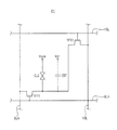
図1は、本発明の一実施例による表示パネルの単位画素に対する等価回路図である。 FIG. 1 is an equivalent circuit diagram for a unit pixel of a display panel according to an embodiment of the present invention.
図1に示すように、単位画素P1は、ゲート配線GLn、データ配線DLm、インパルスゲート配線IGL、及びインパルスデータ配線IDLによって定義される。 As shown in FIG. 1, the unit pixel P1 is defined by a gate line GLn, a data line DLm, an impulse gate line IGL, and an impulse data line IDL.
単位画素P1は、第1スイッチング素子TFT1(単にスイッチング素子と称する場合もある)、液晶キャパシタCLC、ストレージキャパシタCST、及び第2スイッチング素子TFT2(インパルス駆動素子と称する場合もある)を含む。第1スイッチング素子TFT1と第2スイッチング素子TFT2は薄膜トランジスタとして記載されているが、他のスイッチング素子を利用することもできる。 The unit pixel P1 includes a first switching element TFT1 (sometimes referred to simply as a switching element), a liquid crystal capacitor CLC, a storage capacitor CST, and a second switching element TFT2 (sometimes referred to as an impulse drive element). The first switching element TFT1 and the second switching element TFT2 are described as thin film transistors, but other switching elements can also be used.
第1スイッチング素子TFT1は、ゲート配線GLnに電気的に連結された第1ゲート電極、データ配線DLmに電気的に連結された第1ソース電極、及び液晶キャパシタCLCと電気的に連結された第1ドレイン電極を含む。 The first switching element TFT1 includes a first gate electrode electrically connected to the gate line GLn, a first source electrode electrically connected to the data line DLm, and a first electrode electrically connected to the liquid crystal capacitor CLC. Includes a drain electrode.
液晶キャパシタCLCは、第1スイッチング素子TFT1と電気的に連結された第1電極、及び共通電圧Vcomが印加される第2電極を含む。 The liquid crystal capacitor CLC includes a first electrode electrically connected to the first switching element TFT1 and a second electrode to which a common voltage Vcom is applied.
ストレージキャパシタCSTは、第1スイッチング素子TFT1と液晶キャパシタCLCとのそれぞれに電気的に連結された第1電極、及び共通電圧Vstが印加される第2電極を含む。 The storage capacitor CST includes a first electrode electrically connected to each of the first switching element TFT1 and the liquid crystal capacitor CLC, and a second electrode to which a common voltage Vst is applied.
第2スイッチング素子TFT2は、インパルスゲート配線IGLと電気的に連結された第2ゲート電極、インパルスデータ配線IDLと電気的に連結された第2ソース電極、及び液晶キャパシタCLC及びストレージキャパシタCSTと電気的に連結された第2ドレイン電極を含む。 The second switching element TFT2 is electrically connected to the second gate electrode electrically connected to the impulse gate line IGL, the second source electrode electrically connected to the impulse data line IDL, and the liquid crystal capacitor CLC and the storage capacitor CST. A second drain electrode connected to the first electrode.
単位画素P1の駆動を説明すると、次のようである。 The driving of the unit pixel P1 will be described as follows.
ゲート配線GLnからゲート信号が印加されると、第1スイッチング素子TFT1がターンオンしデータ配線DLmに印加されたデータ電圧が液晶キャパシタCLC及びストレージキャパシタCSTにそれぞれ充電される。 When a gate signal is applied from the gate line GLn, the first switching element TFT1 is turned on, and the data voltage applied to the data line DLm is charged to the liquid crystal capacitor CLC and the storage capacitor CST, respectively.
液晶キャパシタCLCに充電されたデータ電圧に基づいて、単位画素P1はデータ電圧に対応する正常階調を表示する。 Based on the data voltage charged in the liquid crystal capacitor CLC, the unit pixel P1 displays a normal gradation corresponding to the data voltage.
一方、所定時間後、インパルスゲート配線IGLにインパルスゲート信号が印加されると、第2スイッチング素子TFT2がターンオンしインパルスデータ配線IDLに印加されたインパルス電圧が液晶キャパシタCLC及びストレージキャパシタCSTにそれぞれ充電される。インパルス電圧はインパルス駆動のための電圧であって、データ電圧に対して低輝度を有するデータ電圧で、一般的にブラック又はグレイに該当するデータ電圧である。 On the other hand, when an impulse gate signal is applied to the impulse gate line IGL after a predetermined time, the second switching element TFT2 is turned on, and the impulse voltage applied to the impulse data line IDL is charged to the liquid crystal capacitor CLC and the storage capacitor CST, respectively. The The impulse voltage is a voltage for impulse driving, is a data voltage having a low luminance with respect to the data voltage, and is generally a data voltage corresponding to black or gray.
インパルス電圧によって液晶キャパシタCLCが充電されることによって、単位画素P1は、インパルス電圧に対応するインパルス階調(例えば、ブラック階調)を表示する。他の一方で、単位画素P1は、第2スイッチング素子TFT2がターンオンすることによって、液晶キャパシタCLCに予め充電されたデータ電圧を放電する。 When the liquid crystal capacitor CLC is charged with the impulse voltage, the unit pixel P1 displays an impulse gradation (for example, a black gradation) corresponding to the impulse voltage. On the other hand, the unit pixel P1 discharges the data voltage precharged in the liquid crystal capacitor CLC when the second switching element TFT2 is turned on.
図2は、本発明の他の実施例による表示パネルの単位画素に対する等価回路図である。 FIG. 2 is an equivalent circuit diagram for a unit pixel of a display panel according to another embodiment of the present invention.
図2に示すように、単位画素P2は、ゲート配線GLn、データ配線DLm、及びインパルスゲート配線IGLによって定義される。 As shown in FIG. 2, the unit pixel P2 is defined by a gate line GLn, a data line DLm, and an impulse gate line IGL.
単位画素P2は、第1スイッチング素子TFT1、液晶キャパシタCLC、ストレージキャパシタCST、及び第2スイッチング素子TFT2’を含む。図2に示した第2スイッチング素子TFT2’は、図1に示した第2スイッチング素子TFT2とは異なり、図1に示したインパルスデータ配線IDLと連結されない。図2に示した第2スイッチング素子TFT2’も薄膜トランジスタではない他のスイッチング素子を適用することができる。ここで、第1スイッチング素子TFT1、液晶キャパシタCLC、及びストレージキャパシタCSTは、前述した図1に示した構成要素と同じなので、詳細な説明は省略する。 The unit pixel P2 includes a first switching element TFT1, a liquid crystal capacitor CLC, a storage capacitor CST, and a second switching element TFT2 '. Unlike the second switching element TFT2 shown in FIG. 1, the second switching element TFT2 'shown in FIG. 2 is not connected to the impulse data line IDL shown in FIG. Other switching elements that are not thin film transistors can also be applied to the second switching element TFT2 'shown in FIG. Here, the first switching element TFT1, the liquid crystal capacitor CLC, and the storage capacitor CST are the same as the components shown in FIG.
第2スイッチング素子TFT2’は、第2ゲート電極、第2ソース電極、及び第3ドレイン電極を含む。第2ゲート電極は、インパルスゲート配線IGLと電気的に連結される。第2ソース電極は、ストレージキャパシタCSTに共通電圧Vstを印加する共通配線(図示せず)と電気的に連結される。ドレイン電極は、液晶キャパシタCLC及びストレージキャパシタCSTと電気的に連結される。 The second switching element TFT2 'includes a second gate electrode, a second source electrode, and a third drain electrode. The second gate electrode is electrically connected to the impulse gate line IGL. The second source electrode is electrically connected to a common wiring (not shown) that applies a common voltage Vst to the storage capacitor CST. The drain electrode is electrically connected to the liquid crystal capacitor CLC and the storage capacitor CST.
第2スイッチング素子TFT2’のソース電極にストレージキャパシタCSTの共通電圧Vstが連結されインパルス駆動をする場合には、表示パネルが無電界(無電圧印加)状態でブラック階調を表示するノーマリブラックモードで動作しなければならない。 When the common voltage Vst of the storage capacitor CST is connected to the source electrode of the second switching element TFT2 ′ and impulse driving is performed, a normally black mode in which the display panel displays a black gradation with no electric field (no voltage applied). Must work with.
単位画素P2の駆動を説明すると、次のようである。 The driving of the unit pixel P2 will be described as follows.
ゲート配線GLnからゲート信号が印加されると、第1スイッチング素子TFT1がターンオンし、データ配線DLmに印加されたデータ電圧が液晶キャパシタCLC及びストレージキャパシタCSTにそれぞれ充電される。 When a gate signal is applied from the gate line GLn, the first switching element TFT1 is turned on, and the data voltage applied to the data line DLm is charged to the liquid crystal capacitor CLC and the storage capacitor CST, respectively.
液晶キャパシタCLCに充電されたデータ電圧に基づいて単位画素P2は、データ電圧に対応する正常階調を表示する。 Based on the data voltage charged in the liquid crystal capacitor CLC, the unit pixel P2 displays a normal gradation corresponding to the data voltage.
一方、所定時間後、インパルスゲート配線IGLにインパルスゲート信号が印加されると、第2スイッチング素子TFT2’がターンオンし、ストレージキャパシタCSTに印加される共通電圧Vstが液晶キャパシタCLC及びストレージキャパシタCSTにそれぞれ充電される。即ち、共通電圧Vstがインパルス電圧になる。 On the other hand, when an impulse gate signal is applied to the impulse gate line IGL after a predetermined time, the second switching element TFT2 ′ is turned on, and the common voltage Vst applied to the storage capacitor CST is applied to the liquid crystal capacitor CLC and the storage capacitor CST, respectively. Charged. That is, the common voltage Vst becomes an impulse voltage.
共通電圧Vstによって液晶キャパシタCLCが充電されることによって、単位画素P2は共通電圧Vstに対応する非正常階調(例えば、ブラック階調)を表示する。即ち、単位画素P2は、第2スイッチング素子TFT2’がターンオンすることによって、液晶キャパシタCLCに予め充電されたデータ電圧を放電する。 When the liquid crystal capacitor CLC is charged by the common voltage Vst, the unit pixel P2 displays an abnormal gradation (for example, a black gradation) corresponding to the common voltage Vst. That is, the unit pixel P2 discharges the data voltage precharged in the liquid crystal capacitor CLC when the second switching element TFT2 'is turned on.
図3は、本発明の一実施例による液晶表示装置の概略的なブロック図である。 FIG. 3 is a schematic block diagram of a liquid crystal display device according to an embodiment of the present invention.
図3に示すように、液晶表示装置は、タイミング制御部110、駆動電圧発生部120、データ駆動部130、ゲート駆動部140、インパルス駆動部150、及び液晶表示パネル160を含む。
As shown in FIG. 3, the liquid crystal display device includes a
タイミング制御部110は、外部装置から入力された制御信号102を駆動周波数に基づいて第1乃至第4制御信号111、112、113、114に変換する。駆動周波数は約60Hz又は75Hzである。
The
制御信号102は、メインクロック信号MCLK、水平同期信号HSYNC、垂直同期信号VSYNC、及びデータイネーブル信号DEを含む。
The
第1制御信号111は、メインクロック信号MCLKを含み、駆動電圧発生部120に提供される。
The
第2制御信号112は、水平開始信号STH及びロード信号TPを含み、データ駆動部130に提供される。
The
第3制御信号113は、第1スキャン開始信号STV1、第1スキャンクロック信号CPV1、及び第1出力イネーブル信号OE1を含み、ゲート駆動部140に提供される。
The
第4制御信号114は、第2スキャン開始信号STV2、第2スキャンクロック信号CPV2、及び第2出力イネーブル信号OE2を含み、インパルス駆動部150に提供される。
The
駆動電圧発生部120は、第1制御信号111に基づいて表示装置を駆動するための駆動電圧を発生する。具体的に、データ駆動部130には基準階調電圧121を出力する。ゲート駆動部140には、第1ゲート電圧122を出力して、インパルス駆動部150には、第2ゲート電圧123を出力する。液晶表示パネル160には、液晶キャパシタの共通電圧Vcom、ストレージキャパシタCSTの共通電圧Vstを出力する。一方、液晶表示パネル160が図1に示すような単位画素構造を有する場合、駆動電圧発生部120はインパルスデータ配線IDLに印加されるインパルス電圧を出力する。
The
データ駆動部130は、第2制御信号112に基づいて画像データ115を、基準階調電圧121に基づくアナログ形態のデータ電圧に変換する。データ駆動部130は、変換されたアナログ形態のデータ電圧(D1、D2、…、DM)を液晶表示パネル160のデータ配線DLに出力する。
The
ゲート駆動部140は、タイミング制御部110から提供された第3制御信号113、及び駆動電圧発生部120から提供された第1ゲート電圧122を利用してゲート信号(G1、G2、…、GN)を生成し、生成されたゲート信号(G1、G2、…、GN)を液晶表示パネル160のゲート配線GLに出力する。
The
インパルス駆動部150は、タイミング制御部110から提供された第4制御信号114、及び駆動電圧発生部120から提供された第2ゲート電圧123を利用してインパルスゲート信号(IG1、IG2、…、IGN)を生成し、生成されたインパルスゲート信号(IG1、IG2、…、IGN)を液晶表示パネル160のインパルスゲート配線IGLに出力する。
The
第3制御信号113のうち、第1スキャン開始信号STV1と、第4制御信号114のうち、第2スキャン開始信号STV2は所定の遅延差を有する。即ち、第2スキャン開始信号STV2は、第1スキャン開始信号STV1が出力され、所定時間だけ遅延された後に出力される。
Of the
結果的に、第2スキャン開始信号STV2によって始まるインパルスゲート信号(IG1、IG2、…、IGN)は、第1スキャン開始信号STV1によってゲート信号(G1、G2、…、GN)が出力された後、所定時間以後から出力される。これによって、液晶表示パネル160は、1フレーム区間の間、データ電圧による正常画面と、インパルス電圧によるインパルス画面が表示される。
As a result, the impulse gate signals (IG1, IG2,..., IGN) starting from the second scan start signal STV2 are output after the gate signals (G1, G2,..., GN) are output by the first scan start signal STV1. Output after a predetermined time. Accordingly, the liquid
液晶表示パネル160は、液晶層と、液晶層を収容する第1及び第2基板を含み、図1及び図2に示した単位画素P1、P2のうちのいずれか一つの画素構造を有する。
The liquid
図4は、図3に示した表示パネルの一実施例による平面図である。 FIG. 4 is a plan view of one embodiment of the display panel shown in FIG.
図4に示すように、表示パネル165は、第1基板161と、第2基板162及び第1及び第2基板161、162の間に介在された液晶層163を含む。
As shown in FIG. 4, the
第1基板161は、表示領域DAと、表示領域DAを取り囲む第1乃至第3周辺領域PA1、PA2、PA3とで構成される。
The
表示領域DAには、第1方向に延長されたデータ配線DL及びインパルスデータ配線IDLと、第1方向と交差する第2方向に配列されたゲート配線GL及びインパルスゲート配線IGLが形成され、データ配線DLとゲート配線GLによって複数の単位画素が定義される。ここで、インパルスデータ配線IDLは、図1に示すように、別の配線で形成することもでき、図2に示すように、別の配線を形成することなく、ストレージキャパシタの共通配線を使用することもできる。 In the display area DA, data lines DL and impulse data lines IDL extended in the first direction, and gate lines GL and impulse gate lines IGL arranged in the second direction intersecting the first direction are formed. A plurality of unit pixels are defined by the DL and the gate wiring GL. Here, the impulse data wiring IDL can be formed by another wiring as shown in FIG. 1, and the common wiring of the storage capacitor is used without forming another wiring as shown in FIG. You can also.
第1周辺領域PA1には、データ配線DLにデータ電圧を出力するデータ駆動チップが搭載されたデータテープキャリアパッケージ(以下、TCP)131が配置される。第2周辺領域PA2には、ゲート配線GLにゲート信号を出力する第1ゲート駆動チップが搭載された第1ゲートTCP141が配置される。第3周辺領域PA3には、インパルスゲート配線IGLにインパルスゲート信号を出力する第2ゲート駆動チップが搭載された第2ゲートTCP151が配置される。
In the first peripheral area PA1, a data tape carrier package (hereinafter referred to as TCP) 131 on which a data driving chip for outputting a data voltage is mounted on the data line DL is disposed. In the second peripheral area PA2, a
第2ゲートTCP151の出力端子は、インパルスゲート配線IGLと一対一でそれぞれ連結される。
The output terminals of the
図5は、図3に示した表示パネルの他の実施例による平面図である。 FIG. 5 is a plan view of another embodiment of the display panel shown in FIG.
図5に示すように、表示パネル265は、第1基板261と、第2基板262及び第1及び第2基板261、262の間に介在された液晶層263を含む。
As shown in FIG. 5, the
第1基板261は、表示領域DAと表示領域DAを取り囲む第1乃至第3周辺領域PA1、PA2、PA3とで構成される。
The
表示領域DAには、第1方向に延長されたデータ配線DL及びインパルスデータ配線IDLと、第1方向と交差する第2方向に配列されたゲート配線GL及びインパルスゲート配線IGLが形成され、データ配線DLとゲート配線GLによって複数の単位画素が定義される。 In the display area DA, data lines DL and impulse data lines IDL extended in the first direction, and gate lines GL and impulse gate lines IGL arranged in the second direction intersecting the first direction are formed. A plurality of unit pixels are defined by the DL and the gate wiring GL.
ここで、インパルスデータ配線IDLは、図1に示すように、別の配線で形成することもでき、図2に示すように、別の配線を形成することなく、ストレージキャパシタの共通配線を使用することもできる。 Here, the impulse data wiring IDL can be formed by another wiring as shown in FIG. 1, and the common wiring of the storage capacitor is used without forming another wiring as shown in FIG. You can also
第1周辺領域PA1にはデータTCP231が配置され、第2周辺領域PA2には第1ゲートTCP242が配置される。第3周辺領域PA3にはインパルスゲート配線IGLにインパルスゲート信号を出力する第2ゲートTCP255が配置される。
The
第2ゲートTCP255の出力端子は、インパルスゲート配線IGLと一対多で連結される配線構造を有する。即ち、一つのゲートTCP出力端子に所定個のインパルス配線IGLが電気的に連結される。
The output terminal of the
これによって、インパルスゲート駆動チップ(又は、ゲートTCP)の個数を減少することができる。例えば、図示したように、3個のインパルスゲート配線に一つの出力端子を連結させて、一対一で連結された図4に示したインパルスゲート駆動チップ(又は、ゲートTCP)より2個減少することができる。 As a result, the number of impulse gate driving chips (or gate TCPs) can be reduced. For example, as shown in the figure, one output terminal is connected to three impulse gate wirings, and the number is reduced by two from the impulse gate driving chip (or gate TCP) shown in FIG. Can do.
以上の図4及び図5では、ゲートTCPを利用して表示パネルにゲート駆動チップが実装される例を図示したが、表示パネルの周辺領域にアモルファスシリコン薄膜トランジスタを実装してゲート駆動回路を具現することもできる。 4 and 5 show an example in which the gate driving chip is mounted on the display panel using the gate TCP. However, an amorphous silicon thin film transistor is mounted on the peripheral area of the display panel to implement the gate driving circuit. You can also
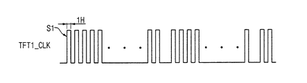
図6乃至図10は、本発明による一実施例のインパルシブ駆動方式を説明するためのタイミング図である。以下では、図3、図4、及び図6乃至図10を参照して説明する。 6 to 10 are timing diagrams for explaining an impulsive driving system according to an embodiment of the present invention. Hereinafter, description will be made with reference to FIGS. 3, 4, and 6 to 10.
タイミング制御部110は、ゲート駆動部140に、図6に示す第1スキャン開始信号STV1を提供する。
The
ゲート駆動部140は、第1スキャン開始信号STV1のハイパルスが印加されると、N個のゲート信号(G1、G2、…、GN)を順次出力する。即ち、1フレームを周期としてN個のゲート信号(G1、G2、…、GN)が順次出力される。一つのゲート信号は、図7に示すように一つの水平区間1Hに対応する。
When the high pulse of the first scan start signal STV1 is applied, the
ゲート信号(G1、G2、…、GN)によって液晶表示パネル160のゲート配線(GL1、GL2、…、GLN)が順次活性化され、これによって第1スイッチング素子TFT1がターンオンする。第1スイッチング素子TFT1がターンオンすると、液晶キャパシタCLCにデータ電圧が充電され、単位画素はデータ電圧に該当する正常階調をそれぞれ表示する。
The gate lines (GL1, GL2,..., GLN) of the liquid
タイミング制御部110は、インパルス駆動部150に、第1スキャン開始信号STV1に対して所定時間だけ遅延された図8に示す第2スキャン開始信号STV2を提供する。
The
インパルス駆動部150は、第2スキャン開始信号STV2のハイパルスが印加されると、N個のインパルスゲート信号(IG1、IG2、…、IGN)を順次出力する。即ち、1フレームを周期としてN個のゲート信号(IG1、IG2、…、IGN)が順次出力される。一つのインパルスゲート信号は、図9に示すように一つの水平区間1Hに対応する。
When the high pulse of the second scan start signal STV2 is applied, the
インパルスゲート信号(IG1、IG2、…、IGN)によって液晶表示パネル160のインパルスゲート配線(IGL1、IGL2、…IGLN)が順次活性化され、これによって第2スイッチング素子TFT2がターンオンして液晶キャパシタCLCに充電されたデータ電圧を放電させる。即ち、第2スイッチング素子TFT2がターンオンすると、インパルス電圧が液晶キャパシタCLCに充電されることによって、単位画素はインパルス階調を表示する。
The impulse gate lines (IGL1, IGL2,... IGLN) of the liquid
図10は、上述のようなインパルシブ駆動による表示パネルの透過率を示すグラフである。図10に示すように、第1スキャン開始信号STV1のハイパルスが出力され、正常画面が表示される区間Dの間は透過率が高い反面、第2スキャン開始信号STV2のハイパルスが出力されインパルス画面が表示される区間Bの間は相対的に透過率が低い。 FIG. 10 is a graph showing the transmittance of the display panel by the impulsive driving as described above. As shown in FIG. 10, while the high pulse of the first scan start signal STV1 is output and the transmittance is high during the period D in which the normal screen is displayed, the high pulse of the second scan start signal STV2 is output and the impulse screen is displayed. The transmittance is relatively low during the displayed section B.
このように、一般駆動速度(例えば、60Hz)で1フレーム区間の間に正常画面とインパルス画面を交互に表示するインパルシブ駆動方式を利用して動画像の表示特性を向上させることができる。 In this way, the display characteristics of moving images can be improved by using an impulsive driving method in which a normal screen and an impulse screen are alternately displayed during one frame period at a general driving speed (for example, 60 Hz).
又、第1スキャン開始信号STV1と第2スキャン開始信号STV2との遅延時間を調整して、1フレーム画面に表示される正常画面とインパルス画面の比率を多様に調整することができる。 Further, by adjusting the delay time between the first scan start signal STV1 and the second scan start signal STV2, the ratio of the normal screen and the impulse screen displayed on the one frame screen can be variously adjusted.
図11乃至図15は、本発明による他の実施例のインパルシブ駆動方式を説明するためのタイミング図である。以下では、図3、図5、及び図11乃至図15を参照して説明する。 11 to 15 are timing diagrams for explaining an impulsive driving system according to another embodiment of the present invention. Hereinafter, description will be made with reference to FIGS. 3, 5, and 11 to 15.
タイミング制御部110は、ゲート駆動部140に、図11に示す第1スキャン開始信号STV1を提供する。
The
ゲート駆動部140は、第1スキャン開始信号STV1のハイパルスが印加されると、図12に示すようにN個のゲート信号(G1、G2、…、GN)を順次出力する。
When a high pulse of the first scan start signal STV1 is applied, the
ゲート信号(G1、G2、…、GN)によって液晶表示パネル160のゲート配線(GL1、GL2、…、GLN)が順次活性化され、これによって第1スイッチング素子TFT1がターンオンする。第1スイッチング素子TFT1がターンオンすると、液晶キャパシタCLCにデータ電圧が充電され、単位画素はデータ電圧に該当する正常階調をそれぞれ表示する。
The gate lines (GL1, GL2,..., GLN) of the liquid
タイミング制御部110は、インパルス駆動部150に、第1スキャン開始信号STV1に対して所定時間だけ遅延された図13に示す第2スキャン開始信号STV2を提供する。
The
インパルス駆動部150は、第2スキャン開始信号STV2のハイパルスが印加されると、N個のインパルスゲート信号(IG1、IG2、…、IGN)を順次出力する。
When the high pulse of the second scan start signal STV2 is applied, the
ここで、図5に示すように、q番目のインパルスゲート信号IGqが3q−2、3q−1、3q番目インパルスゲート配線(IGL(3q−1)、IGL(3q−2)、IGL(3q))に共用に印加される。従って、インパルスゲート信号(IG1、IG2、…、IGN)は、図14に示すように液晶表示パネル160のインパルスゲート配線(IGL1、IGL2、…、IGLN)が3個ずつグルーピングされ同時に印加される。
Here, as shown in FIG. 5, the q-th impulse gate signal IGq is 3q-2, 3q-1, 3q-th impulse gate wiring (IGL (3q-1), IGL (3q-2), IGL (3q) ) To be shared. Accordingly, the impulse gate signals (IG1, IG2,..., IGN) are grouped by three impulse gate lines (IGL1, IGL2,..., IGLN) of the liquid
これによって、3個の水平ライン3Hに該当する第2スイッチング素子TFT2がターンオンし、液晶キャパシタCLCに充電されたデータ電圧を放電させる。即ち、第2スイッチング素子TFT2がターンオンすると、インパルス電圧が液晶キャパシタCLCに充電されることによって、単位画素はインパルス階調を表示する。
As a result, the second switching element TFT2 corresponding to the three
図15は、上述のようなインパルシブ駆動による表示パネルの透過率を示すグラフである。図15に示すように、第1スキャン開始信号STV1のハイパルスが出力され、正常画面が表示される区間Dの間は透過率が高い反面、第2スキャン開始信号STV2のハイパルスが出力されインパルス画面が表示される区間Bの間は相対的に透過率が低い。 FIG. 15 is a graph showing the transmittance of the display panel by the impulsive driving as described above. As shown in FIG. 15, while the high pulse of the first scan start signal STV1 is output and the transmittance is high during the period D in which the normal screen is displayed, the high pulse of the second scan start signal STV2 is output and the impulse screen is displayed. The transmittance is relatively low during the displayed section B.
このように、一般駆動速度(例えば、60Hz)で1フレーム区間の間に正常画面とインパルス画面を交互に表示するインパルシブ駆動方式を利用して動画像の表示特性を向上させることができる。 In this way, the display characteristics of moving images can be improved by using an impulsive driving method in which a normal screen and an impulse screen are alternately displayed during one frame period at a general driving speed (for example, 60 Hz).
又、第1スキャン開始信号STV1と第2スキャン開始信号STV2との遅延時間を調整して、1フレーム画面に表示される正常画面とインパルス画面の比率を多様に調整することができる。 Further, by adjusting the delay time between the first scan start signal STV1 and the second scan start signal STV2, the ratio of the normal screen and the impulse screen displayed on the one frame screen can be variously adjusted.
図16は、本発明の更に他の実施例による表示パネルの単位画素に対する等価回路図である。 FIG. 16 is an equivalent circuit diagram for a unit pixel of a display panel according to still another embodiment of the present invention.
図16に示すように、単位画素P3は、ゲート配線GLn、データ配線DLm、バイアス電圧VLk、及びインパルスゲート配線IGLによって定義される。 As shown in FIG. 16, the unit pixel P3 is defined by a gate line GLn, a data line DLm, a bias voltage VLk, and an impulse gate line IGL.
単位画素P3は、スイッチング素子Ts、駆動素子Td、有機電界発光素子(Organic Light Emitting Element)EL、ストレージキャパシタCST、及びインパルス駆動素子Tiを含む。 The unit pixel P3 includes a switching element Ts, a driving element Td, an organic light emitting element (EL) EL, a storage capacitor CST, and an impulse driving element Ti.
スイッチング素子Tsは、ゲート配線GLnと電気的に連結されたゲート電極と、データ配線DLmに電気的に連結されたソース電極、及び駆動素子Tdと電気的に連結されたドレイン電極を含む。 The switching element Ts includes a gate electrode electrically connected to the gate line GLn, a source electrode electrically connected to the data line DLm, and a drain electrode electrically connected to the driving element Td.
駆動素子Tdは、スイッチング素子Tsと電気的に連結されたゲート電極と、バイアス電圧配線VLkと電気的に連結されたソース電極、及び有機電界発光素子ELと電気的に連結されたドレイン電極を含む。 The driving element Td includes a gate electrode electrically connected to the switching element Ts, a source electrode electrically connected to the bias voltage wiring VLk, and a drain electrode electrically connected to the organic electroluminescence element EL. .
有機電界発光素子ELは、駆動素子Tdと電気的に連結された第1端と、共通電圧Vcomが印加される共通電圧配線(図示せず)と電気的に連結された第2端を含む。 The organic electroluminescent element EL includes a first end electrically connected to the driving element Td and a second end electrically connected to a common voltage line (not shown) to which a common voltage Vcom is applied.
ストレージキャパシタCSTは、バイアス電圧配線VLkと電気的に連結された第1端と、スイッチング素子Ts及び駆動素子Tdと電気的に連結された第2端を含む。 The storage capacitor CST includes a first end electrically connected to the bias voltage line VLk and a second end electrically connected to the switching element Ts and the driving element Td.
インパルス駆動素子Tiは、インパルスゲート配線IGLと電気的に連結されたゲート電極と、有機電界発光素子ELに共通電圧Vcomを印加する共通電圧配線(図示せず)と電気的に連結されたソース電極、及び駆動素子Tdと電気的に連結されたドレイン電極を含む。 The impulse driving element Ti includes a gate electrode electrically connected to the impulse gate wiring IGL and a source electrode electrically connected to a common voltage wiring (not shown) for applying a common voltage Vcom to the organic electroluminescence element EL. And a drain electrode electrically connected to the driving element Td.
単位画素P3の駆動を説明すると、次のようである。 The driving of the unit pixel P3 will be described as follows.
ゲート配線GLnからゲート信号が印加されると、スイッチング素子Tsがターンオンし、データ配線DLmに印加されたデータ電圧が駆動素子Tdに印加される。駆動素子Tdに印加されたデータ電圧は有機電界発光素子ELに印加され、有機電界発光素子ELはデータ電圧に対応して発光する。単位画素P3は、データ電圧に該当する正常階調を表示する。 When a gate signal is applied from the gate line GLn, the switching element Ts is turned on, and the data voltage applied to the data line DLm is applied to the drive element Td. The data voltage applied to the driving element Td is applied to the organic electroluminescent element EL, and the organic electroluminescent element EL emits light corresponding to the data voltage. The unit pixel P3 displays a normal gradation corresponding to the data voltage.
一方、所定時間以後、インパルスゲート配線IGLにインパルスゲート信号が印加されると、インパルス駆動素子Tiがターンオンし、共通電圧Vcomが駆動素子Tdに印加される。駆動素子Tdに印加された共通電圧Vcomは、有機電界発光素子ELに印加され、有機電界発光素子ELは、共通電圧Vcomに応答して消える。即ち、有機電界発光素子ELは放電される。結果的に、共通電圧Vcomはインパルス電圧になって、単位画素P3にブラック階調を表示させる。 On the other hand, when an impulse gate signal is applied to the impulse gate wiring IGL after a predetermined time, the impulse driving element Ti is turned on and the common voltage Vcom is applied to the driving element Td. The common voltage Vcom applied to the driving element Td is applied to the organic electroluminescent element EL, and the organic electroluminescent element EL disappears in response to the common voltage Vcom. That is, the organic electroluminescent element EL is discharged. As a result, the common voltage Vcom becomes an impulse voltage, and the black gradation is displayed on the unit pixel P3.
以上では、インパルス電圧として有機電界発光素子ELに印加される共通電圧Vcomを使用する例を説明したが、別のインパルスデータ配線を形成して別のインパルス電圧を印加することもできるのは自明である。 The example in which the common voltage Vcom applied to the organic electroluminescent element EL is used as the impulse voltage has been described above. However, it is obvious that another impulse data wiring can be formed and another impulse voltage can be applied. is there.
図17は、本発明の他の実施例による有機発光表示装置の概略的なブロック図である。 FIG. 17 is a schematic block diagram of an organic light emitting display device according to another embodiment of the present invention.
図17に示すように、有機発光表示装置は、タイミング制御部310、駆動電圧発生部320、データ駆動部330、ゲート駆動部340、インパルス駆動部350、及びOLED(Organic Light Emitting Display)パネル360を含む。
As shown in FIG. 17, the organic light emitting display includes a
タイミング制御部310は、外部装置から入力された制御信号302を駆動周波数に基づいて、第1乃至第4制御信号311、312、313、314に変換する。駆動周波数は約60Hz又は75Hzである。
The
タイミング制御部310は、外部装置から入力された原始データ304を信号処理して画像データ315として出力する。
The
第1制御信号311は駆動電圧発生部320に提供され、第2制御信号312はデータ駆動部330に提供され、第3制御信号313はゲート駆動部340に提供され、第4制御信号314はインパルス駆動部350に提供される。
The
第3制御信号313は第1スキャン開始信号STV1、第1スキャンクロック信号CPV1、及び第1出力イネーブル信号OE1を含み、第4制御信号314は、第2スキャン開始信号STV2、第2スキャンクロック信号CPV2、及び第2出力イネーブル信号OE2を含む。
The
駆動電圧発生部320は、第1制御信号311に基づいて表示装置を駆動するための駆動電圧を発生する。具体的に、データ駆動部330には基準階調電圧321を出力する。ゲート駆動部340には、第1ゲート電圧322を出力して、インパルス駆動部350には、第2ゲート電圧323を出力する。OLEDパネル360には、有機電界発光素子ELの共通電圧Vcom、バイアス電圧VLを出力する。
The
一方、OLEDパネル360が、図1に示すように、別のインパルスデータ配線IDLが形成された場合には、駆動電圧発生部320はインパルスデータ配線IDLに印加されるインパルス電圧を出力する。
On the other hand, when another impulse data line IDL is formed in the
データ駆動部330は、第2制御信号312に基づいて画像データ315を、基準階調電圧321に基づくアナログ形態のデータ電圧に変換する。データ駆動部330は、変換されたアナログ形態のデータ電圧(D1、D2、…、DM)をOLEDパネル360のデータ配線DLに出力する。
The
ゲート駆動部340は、第3制御信号313及び第1ゲート電圧322を利用してゲート信号(G1、G2、…、GN)を生成し、OLEDパネル360のゲート配線GLに出力する。
The
インパルス駆動部350は、第4制御信号314及び第2ゲート電圧323を利用してインパルスゲート信号(IG1、IG2、…、IGN)を生成し、OLEDパネル360のインパルスゲート配線IGLに出力する。
The
第3制御信号313のうち、第1スキャン開始信号STV1と、第4制御信号314のうち、第2スキャン開始信号STV2は所定の遅延差を有する。即ち、第2スキャン開始信号STV2によって始まるインパルスゲート信号は、第1スキャン開始信号STV1によって始まるゲート信号が出力された後、所定時間以後から出力される。これによって、OLEDパネル360は、1フレーム区間の間、データ電圧による正常画面と、インパルス電圧によるインパルス画面が表示される。
Of the
OLEDパネル360は、図16に示すような単位画素構造P3を有する。OLEDパネル360のインパルスゲート信号の印加方法は、上述した図4及び図5に示すように多様に具現することができ、それに対する詳細な説明は省略する。
The
又、図17に示した有機発光表示装置のインパルシブ駆動方式も、上述した図6乃至図10と、図11乃至図15に示すように多様に具現することができ、それに対する詳細な説明は省略する。 Also, the impulsive driving method of the organic light emitting display device shown in FIG. 17 can be variously implemented as shown in FIGS. 6 to 10 and FIGS. 11 to 15, and detailed description thereof is omitted. To do.
以上、本発明の実施例によって詳細に説明したが、本発明はこれに限定されず、本発明が属する技術分野において通常の知識を有するものであれば本発明の思想と精神を離れることなく、本発明を修正または変更できる。 As described above, the embodiments of the present invention have been described in detail. However, the present invention is not limited to the embodiments, and as long as it has ordinary knowledge in the technical field to which the present invention belongs, without departing from the spirit and spirit of the present invention, The present invention can be modified or changed.
110、310 タイミング制御部
120、320 駆動電圧発生部
130、330 データ駆動部
140、340 ゲート駆動部
150、350 インパルス駆動部
160 液晶表示パネル
360 OLEDパネル
110, 310
Claims (29)
前記ゲート配線にゲート電圧が印加され活性化されることによって、前記データ配線に印加されたデータ電圧を前記液晶キャパシタに伝達するスイッチング素子と、
前記液晶キャパシタに連結されたストレージキャパシタと、
インパルスゲート信号を伝達するインパルスゲート配線と、
前記インパルスゲート配線にインパルスゲート信号が印加され活性化されることによって、共通電圧を前記液晶キャパシタに伝達し、更に前記ストレージキャパシタに伝達するインパルス駆動素子と、を有することを特徴とする表示パネル。 A liquid crystal capacitor formed in a region surrounded by the gate wiring and the data wiring;
A switching element for transmitting a data voltage applied to the data line to the liquid crystal capacitor by applying a gate voltage to the gate line and being activated;
A storage capacitor connected to the liquid crystal capacitor;
An impulse gate wiring for transmitting an impulse gate signal;
A display panel, comprising: an impulse drive element that transmits a common voltage to the liquid crystal capacitor and further transmits to the storage capacitor when an impulse gate signal is applied to the impulse gate wiring and activated.
前記インパルス駆動素子は前記インパルスゲート配線にインパルスゲート信号が印加され活性化されることによってインパルス電圧を前記液晶キャパシタに伝達することを特徴とする請求項1に記載の表示パネル。 An impulse data line to which an impulse voltage is applied in parallel with the data line;
The display panel according to claim 1, wherein the impulse driving element transmits an impulse voltage to the liquid crystal capacitor when an impulse gate signal is applied to the impulse gate wiring and activated.
インパルスゲート信号を伝達するインパルスゲート配線と、
前記有機電界発光素子を駆動させる駆動素子と、
前記ゲート配線にゲート電圧が印加され活性化されることによって、前記データ配線に印加されたデータ電圧を前記駆動素子に伝達するスイッチング素子と、
前記インパルスゲート配線にインパルスゲート信号が印加され活性化されることによって、前記有機電界発光素子に印加された共通電圧を前記駆動素子に伝達するインパルス駆動素子と、を有することを特徴とする表示パネル。 An organic electroluminescence device formed in a region surrounded by the gate wiring, the data wiring, and the power supply voltage wiring and electrically connected to the common voltage wiring;
An impulse gate wiring for transmitting an impulse gate signal;
A driving element for driving the organic electroluminescent element;
A switching element that transmits a data voltage applied to the data line to the driving element by applying a gate voltage to the gate line and being activated;
An impulse driving element that transmits a common voltage applied to the organic electroluminescence element to the driving element by applying an impulse gate signal to the impulse gate wiring and activating the display panel. .
前記インパルス駆動素子は、前記インパルスゲート配線にインパルスゲート信号が印加され活性化されることによってインパルス電圧を前記駆動素子に伝達することを特徴とする請求項6に記載の表示パネル。 An impulse data line to which an impulse voltage is applied in parallel with the data line;
The display panel according to claim 6, wherein the impulse driving element transmits an impulse voltage to the driving element when an impulse gate signal is applied to the impulse gate wiring and activated.
データ電圧を出力するデータ駆動部と、
駆動周波数に基づいて第1制御信号、及び前記第1制御信号より一定時間だけ遅延された第2制御信号を出力するタイミング制御部と、
前記第1制御信号に基づいてゲート信号を出力するゲート駆動部と、
前記第2制御信号に基づいてインパルスゲート信号を出力するインパルス駆動部と、
1フレームの第1区間には前記ゲート信号に応答して前記データ電圧に対応する通常階調を表示し、前記1フレームの第2区間には前記インパルスゲート信号に応答して前記インパルス電圧に対応するインパルス階調を表示する表示パネルと、を有することを特徴とする表示装置。 A drive voltage generator for outputting an impulse voltage;
A data driver for outputting a data voltage;
A timing control unit that outputs a first control signal based on a driving frequency and a second control signal delayed by a predetermined time from the first control signal;
A gate driver that outputs a gate signal based on the first control signal;
An impulse driver that outputs an impulse gate signal based on the second control signal;
A normal gray level corresponding to the data voltage is displayed in response to the gate signal in the first period of one frame, and the impulse voltage is corresponding to the impulse voltage in the second period of the one frame. And a display panel for displaying the impulse gradation.
前記ゲート信号に応答してターンオンし前記液晶キャパシタに前記データ電圧を充電させる第1スイッチング素子と、
前記インパルスゲート信号に応答してターンオンし前記液晶キャパシタに前記インパルス電圧を充電させる第2スイッチング素子と、を有することを特徴とする請求項10に記載の表示装置。 The display panel includes a liquid crystal capacitor that charges a gradation voltage;
A first switching element that is turned on in response to the gate signal to charge the liquid crystal capacitor with the data voltage;
The display device according to claim 10, further comprising: a second switching element that is turned on in response to the impulse gate signal and charges the liquid crystal capacitor with the impulse voltage.
有機電界発光素子を駆動する駆動素子と、
前記ゲート信号に応答してターンオンし前記駆動素子に前記データ電圧を伝達するスイッチング素子と、
前記インパルスゲート信号に応答してターンオンし前記駆動素子に前記インパルス電圧を伝達するインパルス駆動素子と、を有することを特徴とする請求項10に記載の表示装置。 The display panel includes an organic electroluminescent element that displays gradation,
A driving element for driving the organic electroluminescent element;
A switching element that is turned on in response to the gate signal and transmits the data voltage to the driving element;
The display device according to claim 10, further comprising: an impulse driving element that is turned on in response to the impulse gate signal and transmits the impulse voltage to the driving element.
インパルス信号を出力する段階と、
ゲート信号を第1画素の第1データスイッチに出力する段階と、
前記ゲート信号に応答して1フレームの第1区間に前記データ信号に対応する階調を前記第1画素に表示する段階と、
前記ゲート信号より一定時間だけ遅延されたインパルスゲート信号を前記第1画素の第1インパルススイッチに出力する段階と、
前記インパルスゲート信号に応答して前記1フレームの第2区間に前記インパルス信号に対応するインパルス階調を前記第1画素に表示する段階と、を有することを特徴とする表示装置の駆動方法。 Outputting a data signal;
Outputting an impulse signal; and
Outputting a gate signal to the first data switch of the first pixel;
Displaying a gray level corresponding to the data signal on the first pixel in a first section of one frame in response to the gate signal;
Outputting an impulse gate signal delayed by a predetermined time from the gate signal to the first impulse switch of the first pixel;
And displaying an impulse grayscale corresponding to the impulse signal on the first pixel in a second interval of the one frame in response to the impulse gate signal.
前記1フレームの前記第1区間に、他のゲート信号を前記第1画素とは異なる第2画素の第2データスイッチに出力する段階と、
前記1フレームの前記第2区間に、前記インパルスゲート信号又は他のインパルスゲート信号を前記第2画素の第2インパルススイッチに印加する段階と、を更に有することを特徴とする請求項20に記載の表示装置の駆動方法。 Outputting other data signals;
Outputting another gate signal to a second data switch of a second pixel different from the first pixel in the first section of the one frame;
21. The method according to claim 20, further comprising: applying the impulse gate signal or another impulse gate signal to the second impulse switch of the second pixel in the second period of the one frame. A driving method of a display device.
第2画素及び前記1フレームの前記第1区間にデータ電圧を第2画素に出力する第2スイッチング回路を含む第2画素領域と、を有することを特徴とする表示装置。 A first pixel region including a first switching circuit that outputs a data voltage to the first pixel and a first interval of one frame and outputs an impulse voltage to the first pixel in a second interval;
And a second pixel region including a second switching circuit that outputs a data voltage to the second pixel in the first section of the one frame.
Applications Claiming Priority (1)
| Application Number | Priority Date | Filing Date | Title |
|---|---|---|---|
| KR1020050034603A KR20060112155A (en) | 2005-04-26 | 2005-04-26 | Display panel and display device with the same and method for driving thereof |
Publications (2)
| Publication Number | Publication Date |
|---|---|
| JP2006309226A true JP2006309226A (en) | 2006-11-09 |
| JP2006309226A5 JP2006309226A5 (en) | 2009-05-21 |
Family
ID=37186350
Family Applications (1)
| Application Number | Title | Priority Date | Filing Date |
|---|---|---|---|
| JP2006118201A Withdrawn JP2006309226A (en) | 2005-04-26 | 2006-04-21 | Display panel, display device having the same and method of driving the same |
Country Status (5)
| Country | Link |
|---|---|
| US (1) | US20060238476A1 (en) |
| JP (1) | JP2006309226A (en) |
| KR (1) | KR20060112155A (en) |
| CN (1) | CN1854825A (en) |
| TW (1) | TW200643864A (en) |
Cited By (2)
| Publication number | Priority date | Publication date | Assignee | Title |
|---|---|---|---|---|
| CN102254538A (en) * | 2011-09-01 | 2011-11-23 | 南京中电熊猫液晶显示科技有限公司 | Method for reducing unbalance of liquid crystal positive and negative voltages |
| KR101915067B1 (en) | 2011-09-29 | 2018-11-06 | 엘지디스플레이 주식회사 | liquid crystal display device and method of driving the same |
Families Citing this family (12)
| Publication number | Priority date | Publication date | Assignee | Title |
|---|---|---|---|---|
| KR101295192B1 (en) | 2006-06-29 | 2013-08-09 | 엘지디스플레이 주식회사 | The organic electro-luminescence device and method for fabricating of the same |
| US8297319B2 (en) | 2006-09-14 | 2012-10-30 | Brooks Automation, Inc. | Carrier gas system and coupling substrate carrier to a loadport |
| KR101493276B1 (en) * | 2007-05-09 | 2015-02-16 | 삼성디스플레이 주식회사 | Timing controller, liquid crystal display comprising the same and driving method of the liquid crystal display |
| KR101435527B1 (en) * | 2007-07-25 | 2014-08-29 | 삼성디스플레이 주식회사 | Display device |
| JP4710953B2 (en) * | 2007-10-31 | 2011-06-29 | カシオ計算機株式会社 | Liquid crystal display device and driving method thereof |
| KR101502369B1 (en) * | 2007-12-31 | 2015-03-13 | 엘지디스플레이 주식회사 | Liquid crystal display deive and metohd for diving the same |
| KR101480002B1 (en) * | 2008-02-20 | 2015-01-08 | 삼성디스플레이 주식회사 | Display device and driving method thereof |
| CN101561600B (en) * | 2008-04-14 | 2011-10-12 | 北京京东方光电科技有限公司 | Array basal plate of liquid crystal display device |
| CN101726890B (en) * | 2008-10-28 | 2012-05-02 | 瀚宇彩晶股份有限公司 | Embedded capacitive induction input display device |
| CN105869600B (en) * | 2016-06-12 | 2019-02-12 | 深圳市华星光电技术有限公司 | Liquid crystal display and its driving circuit |
| KR20200014957A (en) * | 2018-08-01 | 2020-02-12 | 삼성디스플레이 주식회사 | Display apparatus, method of driving display panel using the same |
| CN111435200A (en) * | 2019-01-11 | 2020-07-21 | 惠科股份有限公司 | Liquid crystal display device, liquid crystal display panel and driving method thereof |
Family Cites Families (16)
| Publication number | Priority date | Publication date | Assignee | Title |
|---|---|---|---|---|
| US5627557A (en) * | 1992-08-20 | 1997-05-06 | Sharp Kabushiki Kaisha | Display apparatus |
| JP2671772B2 (en) * | 1993-09-06 | 1997-10-29 | 日本電気株式会社 | Liquid crystal display and its driving method |
| JP3219640B2 (en) * | 1994-06-06 | 2001-10-15 | キヤノン株式会社 | Display device |
| US5959599A (en) * | 1995-11-07 | 1999-09-28 | Semiconductor Energy Laboratory Co., Ltd. | Active matrix type liquid-crystal display unit and method of driving the same |
| EP0797182A1 (en) * | 1996-03-19 | 1997-09-24 | Hitachi, Ltd. | Active matrix LCD with data holding circuit in each pixel |
| US6724012B2 (en) * | 2000-12-14 | 2004-04-20 | Semiconductor Energy Laboratory Co., Ltd. | Display matrix with pixels having sensor and light emitting portions |
| JP3819723B2 (en) * | 2001-03-30 | 2006-09-13 | 株式会社日立製作所 | Display device and driving method thereof |
| KR100438521B1 (en) * | 2001-05-25 | 2004-07-03 | 엘지.필립스 엘시디 주식회사 | Liquid Crystal Display With Light Shutter and Apparatus and Method of Driving The Same |
| US7230597B2 (en) * | 2001-07-13 | 2007-06-12 | Tpo Hong Kong Holding Limited | Active matrix array devices |
| JP3879463B2 (en) * | 2001-09-19 | 2007-02-14 | 株式会社日立製作所 | Liquid crystal display panel, liquid crystal display device, and liquid crystal television |
| US6943767B2 (en) * | 2002-12-12 | 2005-09-13 | International Business Machines Corporation | Image display device and method of supplying writing electric potential to an image display device |
| JP4390469B2 (en) * | 2003-03-26 | 2009-12-24 | Necエレクトロニクス株式会社 | Image display device, signal line drive circuit used in image display device, and drive method |
| TWI253046B (en) * | 2004-05-12 | 2006-04-11 | Au Optronics Corp | Liquid crystal display with improved motion image quality and driving method therefor |
| JP2006084710A (en) * | 2004-09-15 | 2006-03-30 | Toshiba Matsushita Display Technology Co Ltd | Display control circuit, display control method, and liquid crystal display |
| TWI299850B (en) * | 2004-12-24 | 2008-08-11 | Au Optronics Corp | Dual single-ended driven liquid crystal display and driving method thereof |
| TW200630951A (en) * | 2005-02-21 | 2006-09-01 | Au Optronics Corp | Display panels and display device using same |
-
2005
- 2005-04-26 KR KR1020050034603A patent/KR20060112155A/en not_active Application Discontinuation
-
2006
- 2006-02-09 TW TW095104365A patent/TW200643864A/en unknown
- 2006-02-16 CN CNA2006100090018A patent/CN1854825A/en active Pending
- 2006-03-03 US US11/367,145 patent/US20060238476A1/en not_active Abandoned
- 2006-04-21 JP JP2006118201A patent/JP2006309226A/en not_active Withdrawn
Cited By (2)
| Publication number | Priority date | Publication date | Assignee | Title |
|---|---|---|---|---|
| CN102254538A (en) * | 2011-09-01 | 2011-11-23 | 南京中电熊猫液晶显示科技有限公司 | Method for reducing unbalance of liquid crystal positive and negative voltages |
| KR101915067B1 (en) | 2011-09-29 | 2018-11-06 | 엘지디스플레이 주식회사 | liquid crystal display device and method of driving the same |
Also Published As
| Publication number | Publication date |
|---|---|
| US20060238476A1 (en) | 2006-10-26 |
| KR20060112155A (en) | 2006-10-31 |
| CN1854825A (en) | 2006-11-01 |
| TW200643864A (en) | 2006-12-16 |
Similar Documents
| Publication | Publication Date | Title |
|---|---|---|
| JP2006309226A (en) | Display panel, display device having the same and method of driving the same | |
| US10803810B2 (en) | Display device having black image inserting function | |
| US8199099B2 (en) | Apparatus and method for driving liquid crystal display device | |
| CN1904982B (en) | Display device using enhanced gate driver | |
| US8723853B2 (en) | Driving device, display apparatus having the same and method of driving the display apparatus | |
| US20050078076A1 (en) | Scan driver, display device having the same, and method of driving display device | |
| KR20140042983A (en) | Liquid crystal display device | |
| KR20080006037A (en) | Shift register, display device including shift register, driving apparatus of shift register and display device | |
| US20060279513A1 (en) | Apparatus and method for driving gate lines in a flat panel display (FPD) | |
| US11482184B2 (en) | Row drive circuit of array substrate and display device | |
| KR20130120283A (en) | Liquid crystal display | |
| JP2015018064A (en) | Display device | |
| CN113393790B (en) | Display panel driving method and device and display device | |
| US8605126B2 (en) | Display apparatus | |
| US20080158126A1 (en) | Liquid crystal display and driving method thereof | |
| KR101243540B1 (en) | Liquid crystal display device | |
| US7277092B2 (en) | Method and device for driving liquid crystal display | |
| US20100171725A1 (en) | Method of driving scan lines of flat panel display | |
| CN107731192B (en) | Driving system and method for liquid crystal display | |
| KR20070041829A (en) | Flat panel display and driving method thereof | |
| KR102138664B1 (en) | Display device | |
| US11837173B2 (en) | Gate driving circuit having a node controller and display device thereof | |
| KR101915067B1 (en) | liquid crystal display device and method of driving the same | |
| KR102283377B1 (en) | Display device and gate driving circuit thereof | |
| KR20140038240A (en) | Liquid crystal display and undershoot generation circuit thereof |
Legal Events
| Date | Code | Title | Description |
|---|---|---|---|
| A521 | Request for written amendment filed |
Free format text: JAPANESE INTERMEDIATE CODE: A523 Effective date: 20090402 |
|
| A621 | Written request for application examination |
Free format text: JAPANESE INTERMEDIATE CODE: A621 Effective date: 20090402 |
|
| A761 | Written withdrawal of application |
Free format text: JAPANESE INTERMEDIATE CODE: A761 Effective date: 20110127 |