JP3879463B2 - Liquid crystal display panel, liquid crystal display device, and liquid crystal television - Google Patents
Liquid crystal display panel, liquid crystal display device, and liquid crystal television Download PDFInfo
- Publication number
- JP3879463B2 JP3879463B2 JP2001284356A JP2001284356A JP3879463B2 JP 3879463 B2 JP3879463 B2 JP 3879463B2 JP 2001284356 A JP2001284356 A JP 2001284356A JP 2001284356 A JP2001284356 A JP 2001284356A JP 3879463 B2 JP3879463 B2 JP 3879463B2
- Authority
- JP
- Japan
- Prior art keywords
- electrode
- liquid crystal
- signal
- crystal display
- wiring
- Prior art date
- Legal status (The legal status is an assumption and is not a legal conclusion. Google has not performed a legal analysis and makes no representation as to the accuracy of the status listed.)
- Expired - Fee Related
Links
Images


Classifications
-
- G—PHYSICS
- G02—OPTICS
- G02F—OPTICAL DEVICES OR ARRANGEMENTS FOR THE CONTROL OF LIGHT BY MODIFICATION OF THE OPTICAL PROPERTIES OF THE MEDIA OF THE ELEMENTS INVOLVED THEREIN; NON-LINEAR OPTICS; FREQUENCY-CHANGING OF LIGHT; OPTICAL LOGIC ELEMENTS; OPTICAL ANALOGUE/DIGITAL CONVERTERS
- G02F1/00—Devices or arrangements for the control of the intensity, colour, phase, polarisation or direction of light arriving from an independent light source, e.g. switching, gating or modulating; Non-linear optics
- G02F1/01—Devices or arrangements for the control of the intensity, colour, phase, polarisation or direction of light arriving from an independent light source, e.g. switching, gating or modulating; Non-linear optics for the control of the intensity, phase, polarisation or colour
- G02F1/13—Devices or arrangements for the control of the intensity, colour, phase, polarisation or direction of light arriving from an independent light source, e.g. switching, gating or modulating; Non-linear optics for the control of the intensity, phase, polarisation or colour based on liquid crystals, e.g. single liquid crystal display cells
- G02F1/133—Constructional arrangements; Operation of liquid crystal cells; Circuit arrangements
- G02F1/1333—Constructional arrangements; Manufacturing methods
- G02F1/1343—Electrodes
- G02F1/134309—Electrodes characterised by their geometrical arrangement
- G02F1/134363—Electrodes characterised by their geometrical arrangement for applying an electric field parallel to the substrate, i.e. in-plane switching [IPS]
-
- G—PHYSICS
- G09—EDUCATION; CRYPTOGRAPHY; DISPLAY; ADVERTISING; SEALS
- G09G—ARRANGEMENTS OR CIRCUITS FOR CONTROL OF INDICATING DEVICES USING STATIC MEANS TO PRESENT VARIABLE INFORMATION
- G09G3/00—Control arrangements or circuits, of interest only in connection with visual indicators other than cathode-ray tubes
- G09G3/20—Control arrangements or circuits, of interest only in connection with visual indicators other than cathode-ray tubes for presentation of an assembly of a number of characters, e.g. a page, by composing the assembly by combination of individual elements arranged in a matrix no fixed position being assigned to or needed to be assigned to the individual characters or partial characters
- G09G3/34—Control arrangements or circuits, of interest only in connection with visual indicators other than cathode-ray tubes for presentation of an assembly of a number of characters, e.g. a page, by composing the assembly by combination of individual elements arranged in a matrix no fixed position being assigned to or needed to be assigned to the individual characters or partial characters by control of light from an independent source
- G09G3/36—Control arrangements or circuits, of interest only in connection with visual indicators other than cathode-ray tubes for presentation of an assembly of a number of characters, e.g. a page, by composing the assembly by combination of individual elements arranged in a matrix no fixed position being assigned to or needed to be assigned to the individual characters or partial characters by control of light from an independent source using liquid crystals
- G09G3/3611—Control of matrices with row and column drivers
- G09G3/3648—Control of matrices with row and column drivers using an active matrix
- G09G3/3659—Control of matrices with row and column drivers using an active matrix the addressing of the pixel involving the control of two or more scan electrodes or two or more data electrodes, e.g. pixel voltage dependant on signal of two data electrodes
-
- G—PHYSICS
- G09—EDUCATION; CRYPTOGRAPHY; DISPLAY; ADVERTISING; SEALS
- G09G—ARRANGEMENTS OR CIRCUITS FOR CONTROL OF INDICATING DEVICES USING STATIC MEANS TO PRESENT VARIABLE INFORMATION
- G09G2300/00—Aspects of the constitution of display devices
- G09G2300/04—Structural and physical details of display devices
- G09G2300/0421—Structural details of the set of electrodes
- G09G2300/043—Compensation electrodes or other additional electrodes in matrix displays related to distortions or compensation signals, e.g. for modifying TFT threshold voltage in column driver
-
- G—PHYSICS
- G09—EDUCATION; CRYPTOGRAPHY; DISPLAY; ADVERTISING; SEALS
- G09G—ARRANGEMENTS OR CIRCUITS FOR CONTROL OF INDICATING DEVICES USING STATIC MEANS TO PRESENT VARIABLE INFORMATION
- G09G2300/00—Aspects of the constitution of display devices
- G09G2300/08—Active matrix structure, i.e. with use of active elements, inclusive of non-linear two terminal elements, in the pixels together with light emitting or modulating elements
- G09G2300/0809—Several active elements per pixel in active matrix panels
-
- G—PHYSICS
- G09—EDUCATION; CRYPTOGRAPHY; DISPLAY; ADVERTISING; SEALS
- G09G—ARRANGEMENTS OR CIRCUITS FOR CONTROL OF INDICATING DEVICES USING STATIC MEANS TO PRESENT VARIABLE INFORMATION
- G09G2320/00—Control of display operating conditions
- G09G2320/02—Improving the quality of display appearance
- G09G2320/0252—Improving the response speed
-
- G—PHYSICS
- G09—EDUCATION; CRYPTOGRAPHY; DISPLAY; ADVERTISING; SEALS
- G09G—ARRANGEMENTS OR CIRCUITS FOR CONTROL OF INDICATING DEVICES USING STATIC MEANS TO PRESENT VARIABLE INFORMATION
- G09G2320/00—Control of display operating conditions
- G09G2320/02—Improving the quality of display appearance
- G09G2320/0257—Reduction of after-image effects
Description
【0001】
【発明の属する技術分野】
本発明はアクティブマトリクス型液晶表示パネル、及びアクティブマトリクス型液晶表示装置、及び液晶テレビに関わる。
【0002】
【従来の技術】
液晶表示装置は2枚のガラス基板を所定の間隔をあけて配置し、そのすき間に液晶を注入して構成する。ガラス基板と液晶層の間には配向膜と呼ばれる高分子薄膜を配置し、液晶分子を配列させるために配向処理を施している。表示はこの配列された液晶分子に電界を印加することにより、その配向方向を変化させ、それにより生じる液晶層の光学特性の変化を利用して行う。
【0003】
従来のアクティブ駆動型液晶表示装置では、TN方式に代表されるように、液晶を挟持する一対の基板においてそれぞれの内側に透明電極を設け、これら電極間に生じる基板面に垂直な方向の電界により液晶分子を駆動する。すなわち、この基板に垂直な電界により液晶分子が立ちあがることにより光のスイッチを行う。このような方式では、特に中間調において、液晶パネルを見る方向により色調の反転などを生じ、視野角が狭いことが大きな問題である。
【0004】
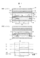
これを解決する一つの手段として、特公昭63−21907号公報によりIPS方式が開示されている。図32及び図33にIPS方式液晶表示装置の画素部の電極構造及び断面図を示した。なお、ここでは特に画素内2分割の電極構造を示した。また、図34には液晶表示装置を駆動するシステム概略図を示した。この方式では、液晶を挟持する一対の基板のうち、一方の基板上に2つの異なる電極、すなわち画素電極106及び共通電極103を形成し、これら電極間に生じる均一な、基板面にほぼ平行な電界5によって、液晶分子を基板面にほぼ平行な面内で回転させることにより光をスイッチする方式である。そのために画面を見る角度(視野角)によって階調,色調の反転が生じることがなく、従来のTN方式に比べ視野角が広い。このような視角特性に優れたIPS方式は、従来のTN方式に変わる新しい液晶表示装置として期待され、今後の大画面液晶モニタや液晶テレビにとって重要な技術である。しかし、現状のIPS液晶表示装置において、今後の液晶テレビやDVDビデオ再生対応モニタなど動画対応ディスプレイへの展開を考えると、応答速度の向上が最大の課題である。
【0005】
IPS方式液晶表示装置の高速応答化については主に液晶材料からの検討が進められてきた。その中で、液晶材料の開発は大きく2つの方向で進められてきた。すなわち、液晶材料の高極性化(高Δε化)と低粘度化である。しかしながら、一般に液晶材料は極性が高くなると粘度も高くなるというトレードオフの関係や、液晶材料の特性が液晶表示装置の表示特性やその信頼性に直接影響することから、材料開発の裕度が制限され、液晶材料開発だけによる高速応答化には限度がある。そこで、現在ではこれら液晶材料の開発に加えて、駆動方法や画素構造の観点から高速応答化へのアプローチも並行して進められている。
【0006】
駆動法による高速応答化については特開2001−34238号公報で提案されている。これは、階調変化分を超える表示データ(オーバードライブ電圧)を画素に入力することで、電圧変化量を大きくし、応答速度の向上を図る方法である。このような方法は一般にオーバードライブ駆動と呼ばれ、階調変化直後に目標透過率を達成するために必要な電圧より高い電圧を一時的に印加することで目的透過率まで到達する時間(応答時間)を早める手段である。なお、後述するがこの手段は中間調でのみ有効である。
【0007】
また、画素構造を変えることによって高速応答化を実現しようとする手段が特開平11−231344号公報や特開平11−316383号公報で提案されている。特開平11−231344号公報では従来のIPS方式液晶表示装置において、画素電極及び共通電極が形成されたアレイ基板(電極基板)の対向基板側に第2の共通電極を形成した構造である。これは、画素電極と第2の共通電極間に生じる電界により、対向基板近傍の液晶分子を有効的に駆動することによって応答速度の向上を図る方法である。また、特開平11−316383号公報では画素電極及び共通電極の電極間距離をセルギャップ(液晶層の厚み)以下に狭めた構造、もしくは画素電極と共通電極を重畳させた構造を用いることにより、特に電極端部で強電界を発生させることにより応答速度を向上させる方法である。
【0008】
【発明が解決しようとする課題】
しかしながら、上記で述べた各手段にはそれぞれ以下に述べる課題を有する。
【0009】
オーバードライブ駆動は中間調でのみ有効な手段であり、全ての階調における応答速度を改善することができないことが、この駆動における最大の課題である。液晶表示装置の液晶層に印加している電圧は通常、交流電圧であり、低電圧側は電圧無印加(V=0V)より下の電圧というものは存在しないことから、電圧無印加状態が表現する階調への応答速度を速めることはできない。また、高電圧側においても、信号線ドライバの電気的耐圧により、画素に印加できる電圧は限られており、通常その電圧は液晶を十分に駆動する電圧(動作電圧)とほぼ等しい。そのため高電圧側においては階調の応答速度を速めるために使える電圧幅(ΔV:オーバードライブ電圧)がほとんどないために、高電圧側が表現する階調への応答速度を速めることはできない。すなわち、オーバードライブ駆動では中間調での応答速度を向上することが可能であり、応答速度の階調依存を平坦化できるが、特に高電圧側の応答速度を改善することはドライバ耐圧の制限により不可能である。
【0010】
一方、画素構造による高速化応答技術については、特に表示性能を劣化させる課題を有する。特開平11−231344号公報に提案されている対向基板側に第2の共通電極を形成する手段では、横電界成分に加え、縦電界成分が増加するために正の誘電率異方性を有する液晶分子においては基板面に対して分子が立ちあがることから、色調など色再現性に問題を生じる。
【0011】
また、特開平11−316383号公報に提案されている電極間隔をセルギャップ(液晶層厚み)以下に狭めた構造では、表示性能を著しく低下させる要因の一つである残像現象を生じる。この残像現象は、本発明者らの検討から、応答速度の向上に有効的に作用している電極端部で生じる強電界が主原因であることがわかった。液晶分子は、電界強度に応じて基板面に平行な面内で回転するが、電極が重畳しているなど極度に電極間隔が狭い場合には、電極端部での電界集中により発生する強電界により液晶層中の液晶分子の平均的な回転角度よりも数倍大きく回転している。例えば、白色を表示させる場合には液晶層中の平均的な液晶分子長軸が偏光板の透過軸に対しておよそ45°回転する必要がある。この液晶分子の回転角には分布があり、実際には電界強度が極度に大きい電極端部近傍では45°以上捻れている。この時、特に電極端部近傍では、この極度に大きな液晶分子の回転により生じた回転トルクが負荷として配向膜表面に伝わり、その結果として配向膜表面の塑性変形が主原因と考えられる残像・焼付き現象を生じる。この残像現象は強電界が保持される時間と大きく相関があり、その保持時間が長いほど悪化する。
【0012】
本発明の目的は、高速応答を実現できる液晶表示パネル、及び液晶表示装置を提供するものである。
【0013】
本発明の別の目的は、表示性能を大きく左右する残像現象を抑制した高品質な液晶表示パネル、及び液晶表示装置を提供することである。
【0014】
【課題を解決するための手段】
本発明の一つの実施態様によれば、一対の基板と、これら一対の基板間に配置した液晶層とを有する液晶表示パネルで、一対の基板の一方の基板に、ある方向に伸びた第1の電極,第2の電極、及び第3の電極を配置し、1フレーム期間内の初期段階と途中段階で、それぞれ第1の電極,第2の電極、または第3の電極に与える電位を変えて表示を制御するというものである。
【0015】
具体的には、第1の電極,第2の電極、及び第3の電極間のそれぞれの電位差について、少なくとも2つの電位差の関係が、1フレーム期間内の初期段階と途中段階で異なるように制御するというものである。
【0016】
さらに、上述の制御をより有効に行う手段として、第3の電極を、第1の電極と第2の電極間の第1の電極により近い位置に配置したというものである。
【0017】
さらに具体的な構成は、第1の電極または第2の電極の一方の電極が第1の能動素子を介して第1の信号線に接続され、第1の電極または第2の電極のうち第1の能動素子に接続されていない他方の電極が共通配線に接続され、第3の電極が第2の能動素子を介して第2の信号線に接続されているというものである。
【0018】
さらには、第1の信号線に交差するように配置され第1の能動素子に接続された第1の走査線を有し、第2の信号線に交差するように配置され第2の能動素子に接続された第2の走査線を有し、第1の信号線,第1の走査線,第2の信号線、及び第2の走査線に囲まれた領域に対応して画素を構成し、この画素を複数配置して表示領域を形成しているというものである。
【0019】
さらには、この表示領域の外側に、第1の信号線に接続された第1の信号駆動回路と、第2の信号線に接続された第2の信号駆動回路と、第1の走査線に接続された第1の走査駆動回路と、第2の走査線に接続された第2の走査駆動回路と、共通配線に接続された共通配線駆動回路を有しているというものである。
【0020】
さらには、この表示領域の外側に、第1の信号駆動回路,第2の信号駆動回路,第1の走査駆動回路,第2の走査駆動回路、及び共通配線駆動回路に接続された表示制御回路を有しているというものである。
【0021】
さらに、具体的な別の構成は、第1の電極または第2の電極の一方の電極が第1の能動素子を介して、及び第3の電極が第2の能動素子を介して信号線に接続され、第1の電極または第2の電極のうち、第1の能動素子に接続されていない他方の電極が共通配線に接続されて、信号線に交差するように配置され第1の能動素子及び第2の能動素子に接続された走査線を有し、信号線,走査線に囲まれた領域に対応して画素を構成し、これらの画素を複数配置して表示領域を形成しており、これらの画素に対応するそれぞれの走査線は、1フレーム期間内に2回走査されるというものである。この2回の走査は、異なる走査電圧値で行うものであり、また第1の能動素子および第2の能動素子は異なる閾値特性を有するというものである。
【0022】
本発明の別の実施態様によれば、少なくとも一方の基板が透明基板である一対の基板と、この一対の基板間に配置した液晶層とを有する液晶表示パネルで、一対の基板の一方の基板には複数の画素により構成される表示領域を有し、この画素内には、ある方向に伸びた第1の電極,第2の電極、及び第3の電極を配置し、1フレーム期間内の初期段階と途中段階で、それぞれ第1の電極,第2の電極、または第3の電極に与える電位を変えて表示を制御するというものである。
【0023】
さらに、これらの第1の電極,第2の電極、及び第3の電極は、独立して電位が与えられ、第1の電極,第2の電極、及び第3の電極間のそれぞれの電位差について、少なくとも2つの電位差の関係が、1フレーム期間内の初期段階と途中段階で異なっているというものである。
【0024】
さらに、この第3の電極は、第1の電極と第2の電極間の第1の電極により近い位置に配置され、第1の電極と第3の電極の電位差と、第2の電極と第3の電極の電位差が、1フレーム期間内の初期段階と途中段階で異なっているというものである。
【0025】
本発明の別の実施態様は、少なくとも一方の基板が透明基板である一対の基板と、この一対の基板間に配置した液晶層とを有する液晶表示パネルで、1フレーム期間内の初期段階と途中段階で、液晶層中に形成される電界を変えて表示を制御するというものである。
【0026】
さらに、1フレーム期間内の初期段階では強電界を形成し、途中段階では初期段階の電界よりも弱い電界を形成するよう電界を変えるというものである。
【0027】
本発明の別の実施態様は、液晶表示装置が、一対の基板と、この一対の基板間に配置した液晶層と、この一対の基板の一方の基板に配置したある方向に伸びた第1の電極,第2の電極、及び第3の電極とを有し、1フレーム期間内の初期段階と途中段階で、それぞれ第1の電極,第2の電極、または第3の電極に与える電位を変えて表示を制御するように構成した液晶表示パネルと、光源と、を有するというものである。
【0028】
本発明の別の実施態様は、液晶テレビが、一対の基板と、この一対の基板間に配置した液晶層と、この一対の基板の一方の基板に配置したある方向に伸びた第1の電極,第2の電極、及び第3の電極とを有し、1フレーム期間内の初期段階と途中段階で、それぞれ第1の電極,第2の電極、または第3の電極に与える電位を変えて表示を制御するように構成した液晶表示パネルと、光源と、この光源を制御するインバータ回路と、チューナーを有するというものである。
【0029】
【発明の実施の形態】
図1を用いて、本発明について説明する。図1(a)は本発明の概要を説明するための液晶パネルの画素部の断面概略図であり、図1(b)は図1(a)で示した各電極の1フレーム周期内における電位変化の例を示している。
【0030】
図1(a)の構成は、例えばガラス基板やプラスチック基板、またはガラス基板とプラスチック基板を張り合わせた基板のような少なくとも一方が透明な一対の基板7及び8に液晶層14を挟持して構成されている。基板7,8にはそれぞれ偏光板15が配置されており、基板7には後述する電極を配置し、さらにこれらの電極上には絶縁膜9,10及び配向膜11が形成されている。また、基板8にはカラーフィルタ12及びカラーフィルタ12の保護膜となるオーバーコート膜13,配向膜11が形成された構成である。尚、このカラーフィルタは特に基板8側に形成する必要がなく、基板7側に配置しても良い。
【0031】
基板7には複数の画素により構成された表示領域が形成されており、図1(a)は、これらの各画素の断面図を示したものである。即ち、本発明では、基板7に形成された表示領域中の各画素内に線状若しくは櫛歯状の形状をした第1の電極1,第2の電極2、及び第3の電極を配置した電極構成であり、各電極(第1の電極1,第2の電極2、及び第3の電極3)には独立に電位を与えることができるようにしているというものである。さらに、1フレーム期間内の初期段階と途中段階で、それぞれ第1の電極,第2の電極、または第3の電極に与える電位を変えて表示を制御するというものである。即ち、1フレーム期間内で各電極に与える電位を変えることによって、液晶層中に形成される電界を変化させるというものである。詳しくは、第1の電極,第2の電極、及び第3の電極間のそれぞれの電位差について、少なくとも2つの電位差の関係が、1フレーム期間内の初期段階と途中段階で異なるようにするこで、この電界の変化を実現しようというものである。
【0032】
具体的には、図1(a)のように、1フレーム期間内の初期段階(t0 <t<t1 )では、第1の電極1と第3の電極3との間に電界4が発生するように電位を与え、この電界4によって液晶層14の第1の電極1及び第3の電極3付近の液晶分子を制御し、次に、図(b)のように、1フレーム期間内の途中段階(t0<t<t1 )では、第1の電極1と第3の電極3との間に電界4を発生させないように電位を与え、液晶層中には電界5のみで液晶層14の液晶分子を制御するというものである。
【0033】
即ち、1フレーム周期内の初期段階(t0<t<t1)では、液晶層中に強電界を発生させ、1フレーム期間内の途中段階(t0<t<t1)で、初期段階に発生させた電界よりも小さい電界を発生させるというものである。
【0034】
また、後述する残像現象の抑制を考えれば、初期段階から途中段階の切り替えは、長くとも1フレーム周期の半分以下の時間(0<t<(t2−t0)/2)内に行うことが望ましい。
【0035】
尚、第1の電極1は画素電極もしくは共通電極のどちらか一方の電極であり、第2の電極2は第1の電極と異なる電極、即ち、第1の電極1が画素電極の場合には第2の電極2は共通電極であり、第1の電極1が共通電極の場合は第2の電極2は画素電極である。
【0036】
また、上述したような1フレーム期間中の電界制御は、第1の電極1,第2の電極2、及び第3の電極3の各電極に所望の電位を与えれば制御可能であるので特に第1の電極1,第2の電極2、及び第3の電極3の配置位置の関係は問題ではない。しかし、電界は各電極間の距離に応じて強さが決まるものであり、より有効に上述の電界の制御を行う場合には、第1の電極1,第2の電極2、及び第3の電極3の配置位置の関係は重要である。
【0037】
よって、図1(a),(b)では有効に上述の電界制御を行うための電極配置として、3つの電極のうち1つの電極(例えば第3の電極)を、残りの2つの電極(この場合には第1の電極と第2の電極)のうちのどちらか一方(例えば第1の電極)により近づけて配置している。このように配置することで、より有効に上述の電界制御が可能となる。
【0038】
さらに、第1の電極1と第3の電極3との電位差をΔV1 ,第1の電極1と第3の電極3との距離をdL ,第2の電極2と第3の電極3との電位差をΔV2 ,第2の電極2と第3の電極3との距離dH とした場合に、1フレーム周期内の初期段階(t0<t<t1)には下記に示した(式1)を満足し、1フレーム周期の途中段階(t1<t<t2)では(式2)を満足するように駆動する。
【0039】
【数1】

【数2】
また、後述する残像現象の抑制を考えれば、電位差ΔV1 が、長くとも1フレーム周期の半分以下の時間(0<t<(t2−t0)/2)内に小さくなるように駆動することが望ましい。
【0042】
この電極構造及び第3の電極電位を1表示期間内で変化させることにより残像現象を抑制した高速応答が可能な液晶表示装置を実現できる。以下、高速応答を実現できる理由と残像現象を抑制できる理由について詳しく説明する。
【0043】
図1(b)に示した各電極の電位変化の例に基づき説明する。1フレーム周期内での初期段階(t0<t<t1)においては、第2の電極と第3の電極が実質的にほぼ同電位(V2≒V3)であり、液晶層中には第1の電極1と第2の電極2の間に印加されるほぼ均一な横電界5と、第1の電極1と第3の電極3の間に印加される電界4により液晶分子を駆動する。第2の電極2と第3の電極3の電位は実質的にほぼ同電位であるが、第1の電極1までの距離が異なる(dL<dH)ことから、第3の電極と第1の電極との間に生じる電界4の強度は、第2の電極と第1の電極との間に生じる電界5の強度よりも大きくなる。
【0044】
液晶分子は電界により従って回転して向きを変え、その回転は電界強度が大きいほど高速かつ大きい。そのために、第1の電極と第3の電極近傍に存在する液晶分子は、これら電極間に生じるより大きな電界4により高速かつ大きく回転する。一方、第1の電極と第2の電極間に存在する液晶分子は、基本的にこれら電極間に生じるほぼ均一な横電界5により駆動される。しかしながら、液晶は連続体として考えられ、液晶の弾性効果により、大きな電界4で高速に駆動された液晶分子が、均一横電界5で緩やかに駆動している液晶分子を引きずる効果を有する。そのために、第1の電極1と第2の電極2の間にある液晶分子は、均一な横電界5に応じて回転するのに加えて、より大きな電界4により高速に駆動された液晶分子に引きずられ、従来の均一な横電界だけで液晶分子を駆動する横電界方式の液晶表示装置に比べ高速応答を実現することが可能である。
【0045】
さらに、強電界の効果を考え液晶分子の高速応答化を実現するためには次のような構造が有効である。
【0046】
一つは、第1の電極1と第2の電極2のうち、第3の電極3との距離が近い側に配置された電極(図中では第1の電極1)と、第3の電極との距離(dL )をより近づける構造である。
【0047】
また一つは、図2(a)に示したように第1の電極と第2の電極のうち、第3の電極との距離が近い側に配置された電極(図中では第1の電極1)と、第3の電極3とが画素表示領域内で少なくとも一部分が重畳している構造が望ましく、さらには部分的に重畳している電極の合わせマージンを考慮すると、ほぼ全面で重畳している図2(b)に示した構造が望ましい。なぜなら、電極が重畳することにより、重畳した電極の端部では電界集中を生じやすく、より大きな電界が発生するからである。従って、本発明を実施するためには非常に有効である。またこの時、重畳している一組の電極のうち、下層に配置されている電極(図中では第3の電極3)幅が、その上層に配置されている電極(図中では第1の電極1)の幅より広い構造が望ましい。電極が重畳し、かつ重畳した下層の電極幅を広くすることによりこれら電極端部で有効に強電界を発生させることができるというものである。
【0048】
さらに図2(a)や図2(b)に示したように電極が重畳している場合には、少なくとも下層に配置されている電極がITOなどの透明導電膜であることが望ましい。上述したように重畳した電極の端部では強電界により液晶分子は高速に駆動される。そのために、他の領域に比べて電圧印加開始後、最初に光が透過する。下層電極が透明電極である場合には、このような領域の光を利用できるために、画素全体の応答時間がより短縮できる。特に応答速度が遅いといわれる中間調表示での応答時間の短縮が期待できる。
【0049】
なお、電極が重畳している場合には、電極間隔dL は、それら電極間に介在する絶縁膜9の膜厚にほぼ等しい。
【0050】
この強度の異なる電界を形成するには、通常の表示に必要な電界の他に、この電界と同じ方向の成分を持つ別の電界を形成すれば良いが、より有効に電界形成し高速化を実現するためには上述の(式1)で示したように、少なくとも図1(a)で示した第1の電極1と第3の電極3との間に生じる電界4の強度が第1の電極1と第2の電極2との間に生じる電界5の強度より大きくすることが望ましい。
【0051】
なお、各電極が配置される層として、図1(a)では第1の電極1が、第2の電極2及び第3の電極3と異なる層に配置されているが、本発明による高速応答化の効果を得るためには、電極が重畳する場合を除いて、これらすべての電極が同層に配置されていてもよい。
【0052】
以上により、強電界の効果を考慮して液晶分子の高速応答化を実現するための構造及び駆動方法を説明したが、一方でこの強電界は高速応答化には非常に有効であるが、液晶表示性能を著しく劣化させる要因の一つである残像現象を発生させるという副作用を有することがわかった。特に図2(a)及び(b)に示したような電極が重畳している構造においてはその副作用は顕著に現れる。
【0053】
上述したように本発明者らの検討から、部分的に発生する非常に大きな電界により液晶分子が液晶層中の平均的な液晶分子の回転角度よりも数倍大きく回転している場合には、液晶分子の回転で生じる回転トルクにより、配向膜表面の塑性変形が主原因と考えられる残像を生じることがわかった。さらに、この残像現象は大きな回転トルクが保持される時間、すなわち強電界が保持される時間と大きく相関があり、その保持時間が長いほど悪化することがわかった。従って、液晶分子に強電界が印加されても、その保持時間を短縮することで残像を抑制することができることを見出した。
【0054】
そこで、本発明ではこれらのことに着目し、まず1フレーム周期内の初期段階(t0<t<t1)には強電界を発生させ、液晶分子を高速に応答させる。その後、例えば図1(b)に示したように、第3の電極電位V3 を第1の電極電位V1 との差が小さくなるように変化させることにより、1フレーム周期内で時間tがt1<t<t2を満たす領域(途中段階)では強電界成分をほぼなくし、第1の電極1と第2の電極2により生じる均一な横電界5と第3の電極3と第2の電極2により生じる均一な横電界6により液晶を駆動する。このように構成することにより、強電界は1フレーム期間中の初期段階である一時的(t0<t<t1)にしか印加されないために残像現象を生じることがなくなる。
【0055】
以上のような電極構造及び1フレーム周期内の各電極の電位変化を有する構成により、高速応答化と残像抑制を両立できる液晶表示装置を得ることができる。さらに本構成では、電極間隔を例えば液晶層の厚み以下に狭めることにより電界強度を大きくし液晶分子を駆動しているために、オーバードライブ駆動のようにドライバ耐圧による制限がなく、全階調に対して高速応答化を実現できる。
【0056】
以下、本発明を具体的に実施するための電極及び配線構造と、各電極及び配線へ供給される信号波形について実施例で説明する。なお、本実施例で示した画素構造は、画素内2分割であり、また、第3の電極が共通電極もしくは画素電極と重畳した構造であるが、本発明は特にこれら画素構造に限定されるものではない。また、各電極及び配線に供給される信号波形についても、実施例で示した信号波形に限定されるものではない。
【0057】
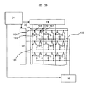
(実施例1)
本実施例の構成を図3,図4,図5,図6,図7を用いて説明する。図3は画素部の電極構造を説明するための図である。図4は本実施例の液晶表示パネルにおける画素部断面図である。図5は図3における各電極及び配線に供給される信号波形を示す図である。図6はこれらの画素構成を有する液晶表示装置全体構成を説明する図である。尚、本明細書では、前述した図1や図4に示した一対の基板及び液晶層、一対の基板に配置した電極等を含めて液晶表示パネルということにし、この液晶表示パネルと光源等を組合せたシステム構成を液晶表示装置ということにする。
【0058】
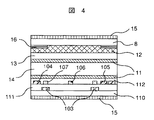
本実施例における液晶表示パネルは、表示部が対角14.1 インチサイズであり、一対の基板は共に透明なガラス基板であり、厚みは0.7mm である。まず、ガラス基板110上に走査配線101,102及び共通電極103を形成する。次に第1の絶縁膜111が窒化シリコンSiNxを用いて形成され、その上に信号配線104,105,画素電極106,第3の電極107が形成されている。電極材料としてはクロムモリブデン(CrMo)を用いている。信号配線104,105や走査配線101,102の材料には電気抵抗の低いものであれば特に問題はなく、アルミニウムや銅,銀もしくはこららの合金等が考えられる。さらに、これら電極上に第2の絶縁膜112が窒化シリコン(SiNx)を用いて形成されている。なお、マトリクス状に形成された第1の走査配線101と第1の信号配線104の交点付近に、能動素子として機能するアモルファスシリコンを用いて作製される第1のTFT108が配置され、第2の走査配線102と第2の信号配線105の交点付近に、能動素子として機能するアモルファスシリコンを用いて作製される第2のTFT109が配置され、これらマトリクス状に形成される各配線に囲まれた領域に対応して画素を形成している。なお、本実施例では能動素子としてアモルファスシリコンを用いたが、ポリシリコンにより形成されたTFTでもよい。ポリシリコンTFTではアモルファスシリコンに比べ移動度が2桁ほど大きいために、以下2つの利点を有する。第1の利点は、アモルファスシリコンTFTに比べチャネル領域の幅を小さくできることからTFTサイズを小さくできることである。本実施例のように1画素内に2つの能動素子を形成する場合には、能動素子のサイズが開口率に大きく寄与するために、小サイズのポリシリコンTFTが有効である。第2の利点は、高速でスイッチングできることである。後述するように、本発明を実施するためには電極構造によっては1フレーム周期内で2回もしくは複数回走査する必要がある。このような場合には高速でスイッチングでき、短い時間で書きこみが可能なポリシリコンTFTが有効である。
【0059】
本電極構造では、図3に示したように一つの画素を駆動するために、2つのTFT,2本の走査配線,2本の信号配線を有している。すなわち、表示部を構成する各画素において、一つの画素内に2つの薄膜トランジスタ(TFT)が形成され、画素電極106が、信号を供給するための第1の信号配線104に、第1のTFT108を介して接続され、この第1のTFT108は第1の走査配線101からの走査信号により走査される。
【0060】
一方、強電界成分を発生させるための第3の電極107が、信号を供給するための第2の信号配線105に第2のTFT109を介して接続され、この第2のTFT109は第2の走査配線102からの走査信号により走査される。ここで、共通電極103は走査配線101,102と同層に形成され、この共通電極103の上に第3の電極107が第1の絶縁膜111を介して重畳している。
【0061】
一方、TFTを形成したガラス基板110に対向するガラス基板8はストライプ状の3色RGBカラーフィルタ12とブラックマトリクス16を兼ね備えた構成である。カラーフィルタ12とブラックマトリクス16上には平坦化するためのオーバーコート樹脂13を形成する。なお、オーバーコート樹脂としてはエポキシ樹脂などを用いる。
【0062】
このようにして作製される各ガラス基板表面に、液晶分子を配向させるためのポリイミド配向膜11を、膜厚100nmで形成する。一般にポリイミド膜は、その前駆体であるポリアミック酸を基板表面に印刷機などで塗布し、これらを高温で焼成することにより形成される。ここで形成されたポリイミド配向膜11の表面をラビング処理することにより配向処理を施す。ラビング方向は画素電極106の長手方向から15°傾いた方向である。
【0063】
本実施例においては、画素内に配置された電極(画素電極,共通電極,第3の電極)は櫛歯状に形成されているが、図7に示すように電極延長方向に対して角度θを有するくの字型に形成されていてもよい。くの字型に形成されることにより、電圧が印加された場合に液晶分子の回転方向が異なる領域を生じ、これにより色付きを抑制することができる。ただし、くの字型電極の場合には液晶分子の初期配向方向として、例えばポジ型液晶の場合には液晶分子の長軸が画素の長手方向と一致するように配向処理する必要がある。
【0064】
次に、これら一対の基板のうち、一方の基板の表示領域周縁部に熱硬化型のシール材を塗布し、もう一方の対向基板を重ね合わせる。なお、シール材は、後に液晶素子内に液晶を注入するための封入口が形成されるように塗布される。加熱しながら加圧し、両基板を接着固定する。基板間には直径4マイクロメートルの高分子ビーズが分散され、基板間の間隔を保持できるようになっている。その後、封入口から真空封入法により液晶を液晶表示素子内に注入し、封入口を紫外線硬化樹脂などで封止する。なお、ここでは液晶材料として分子構造内にシアノ基を有するシアノ系液晶(誘電率異方性が正)を使用する。
【0065】
組合せた基板の両面に偏光板15をノーマリークローズ特性(低電圧で黒表示、高電圧で白表示)となるようにクロスニコル配置で貼りつける。
【0066】
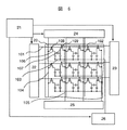
また図6に示すように、各配線は基板の端部まで延在配置され、第1の信号配線104,第2の信号配線105,第1の走査配線101,第2の走査配線102,共通電極103はそれぞれに対応して第1の信号電極駆動回路24,第2の信号電極駆動回路25,第1の走査電極駆動回路22,第2の走査電極駆動回路23,共通電極駆動回路26に接続される。また、各駆動回路は表示制御装置21により制御されている。なお、破線で囲まれた表示画素部20には一つの画素に対応する本電極構造に相当する等価回路を示している。
【0067】
その後、図8で示したシールドケース32,拡散板33,導光板34,反射板35,光源であるバックライト36,下側ケース37,インバータ回路38を組合せることにより液晶表示装置39を組み立てた。
【0068】
このようにして得られる液晶表示装置において、図5に示したような信号波形を各配線及び電極に印加することによって、本発明の効果を得ることができる。以下、各電極及び配線へ印加する信号波形について説明する。
【0069】
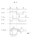
図5(a)は第1の走査配線101に供給される信号波形VG1、(b)は第1の信号配線104に供給される信号波形VD1、(c)は第2の走査配線102に供給される信号波形VG2、(d)は第2の信号配線105に供給される信号波形VD2、(e)は共通電極103に印加される信号波形VC 、(f)は画素内に配置した各電極(画素電極106,共通電極103,第3の電極107に印加される信号波形(画素電極VS ,共通電極VC ,第3の電極VA )を示す。
【0070】
まず第1の走査配線101からの走査信号によりt=t0において第1のTFTがオン状態となり、画素電極106には第1の信号配線104からの電圧が印加される。一方、第2の信号配線105には第1の信号配線104と位相の異なる信号を供給し、かつt=t1 において第2のTFTがオン状態になるよう駆動し、第2の信号配線105からの電圧が第3の電極107に印加される。また、共通電極103の電位VC は第1の信号波形VD1と同期をとり、かつその位相が逆になるよう駆動する。このような駆動においては、1フレーム周期内の初期状態(t0<t<t1)では、画素電極106と共通電極103との間に生じる均一な横電界に加えて、第3の電極107と共通電極103の間に生じる電位差VA−VC (図中矢印)により強電界を生じる。第3の電極107近傍の液晶分子はこの強電界により高速で駆動され、また、共通電極103と画素電極106の間の液晶分子は均一な横電界で駆動されるのに加え、強電界により駆動される液晶分子に引きずられるために全体として従来のIPSに比べ高速応答化が可能である。その後、フレーム周期内の後期(t1<t<t2)においては、第3の電極107の電位VA は共通電極103の電位VC とほぼ同程度になるため、初期のような強電界は発生せず、液晶分子は画素電極106と共通電極103との間に発生する均一な横電界によってのみ駆動される。
【0071】
次に、ここで得られる液晶表示装置を用いて、応答速度及び残像に関して評価した。応答速度は、ホトダイオードを組合せたオシロスコープを用いて評価した。
【0072】
まず、画面上には全面黒色パターンを表示し、その後、最大輝度に相当する白色パターンを表示する。このときの輝度変化をオシロスコープにて読み取り、変化前の輝度B0 から変化後の輝度Bfin への変化量を100%とし、そのうちの90%の変化が終了した時点をもって応答時間とする。本実施例の液晶表示装置において、同一の液晶材料を用いた場合に従来IPSに比べ応答時間が短縮されたことを確認した。
【0073】
次に残像評価について説明する。残像を定量的に評価するためホトダイオードを組合せたオシロスコープを用いて評価した。画面上に最大輝度でウィンドパターンを30分間表示し、その後、残像が最も目立つ中間調表示、ここでは輝度が最大輝度の10%となるように表示画面全面を切り替え、ウィンドの残像部分と周辺中間調部分での輝度Bにおける輝度変動分の大きさΔB/B10% を残像強度として評価した。液晶表示装置の表示特性として残像現象が問題のないレベルは残像強度が2%以下とされており、本実施例で得られた液晶表示装置においては2%以下を達成している。また、この実施例では、後述する実施例2の構造のように第1の電極106と第3の電極107を重畳させる構造ではないため、第1の電極を第3の電極と異なる層に配置するためのスルーホールの形成の必要がない。
【0074】
尚、本発明は本実施例で示した画素内2分割の構造に限られるわけでなく、例えば画素内4分割の構造、あるいはそれ以上の分割数を有する画素構造でもよい。特に精細度の低い液晶表示装置などでは、1画素当たりのピッチが広いために2分割構造では電極間隔が広くなり駆動電圧が上昇してしまう。従って、適当な電極間隔を得るために、精細度に応じて画素の分割数を変える必要がある。
【0075】
図9に画素内4分割の構造を示す。この構造については、第3の電極107は共通電極103に重畳している。特に本図では以下の問題を考慮して第3の電極107を画素中央部の共通電極103に重畳させている。
【0076】
画素を設計する上で、重要な課題の一つは、信号配線104,105から画素内電極(例えば画素電極となる第1の電極106,第3の電極107)へのノイズを低減することである。この信号配線104,105からのノイズにより特に画素電極の電位が変動し、輝度を変動させるからである。従って、図9では第3の電極107は、1画素内に信号配線104,105方向に伸びた3本の第2の電極103(共通電極)のうち中央に配置された第2の電極にのみ重畳させて配置して信号配線104,105からのノイズを受けないようにしている。つまり、3本の第2の電極103の両端の2本の第2の電極で画素内電極をノイズからシールドし、中央の第2の電極と第3の電極により強電界を発生させているということである。
【0077】
このような画素構造においても、1フレーム期間内の初期段階では画素内中央部の共通電極と第3の電極107によって強電界を発生させ、本発明の効果を十分に得ることが可能である。
【0078】
尚、画素を2分割以上の構造にする場合であっても、図9と同様に複数本配置した第2の電極の両端の電極には第3の電極を重畳させないように配置し、両端以外の第2の電極に第3の電極を重畳させる構造とすることで、画素分割数に関わらず同様に適用でき、同様の効果を奏する。
【0079】
(実施例2)
本発明における別の実施例の構成について、図10,図11を用いて説明する。図10は画素部の電極構造を説明するための図である。図11は図10のように配置された各電極及び配線に供給される信号波形について説明する図である。
【0080】
本実施例における液晶表示パネルの構成と、実施例1の液晶表示素子との構成の違いは、第3の電極107が画素電極106と重畳している点である。この構成に伴い、画素電極106は第1の信号配線104が配置されている層より上層に配置する必要があり、図9に示すように画素電極106はスルーホール113を介してさらに上層に配置され、第3の電極107と重畳している。また、第3の電極107が画素電極106に重畳していることから、各電極及び配線に供給される信号波形も実施例1と異なる。その他、電極構造以外の縦構造(配向膜形成,カラーフィルタ形成など)や、画素の等価回路的構成については実施例1と同様である。
【0081】
本実施例での各電極及び配線へ供給される信号波形について図11に示す。以下、各電極及び配線へ印加する信号波形について説明する。
【0082】
図11(a)は第1の走査配線101に供給される信号波形VG1、(b)は第1の信号配線104に供給される信号波形VD1、(c)は第2の走査配線105に供給される信号波形VG2、(d)は第2の信号配線105に供給される信号波形VD2、(e)は共通電極103に印加される信号波形VC 、(f)は画素内の電極(画素電極106,共通電極103,第3の電極107)に印加される信号波形(画素電極VS ,共通電極VC ,第3の電極VA )を示す。
【0083】
まず第1の走査配線101からの走査信号によりt=t0 において第1のTFTがオン状態となり、画素電極106には第1の信号配線104からの電圧が印加される。一方、第2の信号配線105には第1の信号配線104と位相の異なる信号を供給し、かつt=t1 において第2のTFTがオン状態になるよう駆動し、第2の信号配線105からの電圧が第3の電極107に印加される。また、共通電極103の電位VC は一定である。このような駆動においては、1フレーム周期内の初期段階(t0<t<t1)では、画素電極106と共通電極103との間に生じる均一な横電界に加えて、第3の電極107と画素電極106の間に生じる電位差VS−VA(図中矢印)により強電界を生じる。第3の電極107近傍の液晶分子はこの強電界により高速で駆動され、また、共通電極103と画素電極106の間の液晶分子は均一な横電界で駆動されるのに加え、強電界により駆動される液晶分子に引きずられるために全体として従来のIPSに比べ高速応答化が可能である。その後、フレーム周期内の途中段階(t1<t<t2)においては、第3の電極107の電位VA は画素電極106の電位VA とほぼ同程度になるため、初期のような強電界は発生せず、液晶分子は画素電極106と共通電極103との間に発生する均一な横電界によってのみ駆動される。
【0084】
ここで得られる液晶表示装置を用いて、応答速度及び残像に関して評価した。本実施例の液晶表示装置において、同一の液晶材料を用いた場合に従来IPSに比べ応答時間が短縮されたことを確認した。また、本実施例で得られた液晶表示装置においては残像強度2%以下を達成している。
【0085】
本実施例においても、実施例1と同様に画素内2分割の構造に限らず、4分割あるいはそれ以上の分割数を有する画素構造でもよい。
【0086】
図12に画素内4分割の構造を示す。ここで、第3の電極107は画素電極106に重畳した構造である。このような画素構造においても、1フレーム期間内の初期段階では画素電極106と第3の電極107によって強電界を発生させ、本発明の効果を十分に得ることが可能である。この実施例2の4分割構造の場合には、実施例1の4分割構造の場合と比較して、2組の第1の電極及び第3の電極が重畳しているので、より低電圧駆動で有効に強電界を発生させることができる。
【0087】
また、本画素構造においても信号配線104,105に沿って共通電極103となる幅の広い第2の電極を配置することにより信号配線から画素電極へのノイズを遮蔽することができ、実施例1で述べたような課題を解消できる。
【0088】
(実施例3)
本発明における別の実施例の構成について、図13,図14,図15を用いて説明する。図13は画素部の電極構造を説明するための図である。図14は各電極及び配線に供給される信号波形示す図である。図15はこれらの画素構成を有する液晶表示パネルの全体構成を説明する図である。
【0089】
本実施例における液晶表示パネルの構成と、実施例1の液晶表示パネルの構成との差異は、一つの画素内に配置された2つのTFTを1つの走査配線により駆動する点である。実施例1に比べて走査配線を一つに減らすことにより第2の走査配線駆動ドライバが不要となるという効果がある。
【0090】
本電極構造では、図13に示したように一つの画素を駆動するために、2つのTFT,1本の走査配線,2本の信号配線を有する。すなわち、表示部を構成する画素において、一つの画素の内に2つの薄膜トランジスタ(TFT)が形成され、画素電極106が、信号を供給するための第1の信号配線104に、第1のTFT108を介して接続され、一方、強電界成分を発生させるために必要な第3の電極107が、信号を供給するための第2の信号配線105に第2のTFT109を介して接続され、かつ第1のTFT108及び第2のTFT109が共に一つの第1の走査配線101からの走査信号により走査される。ここで、共通電極103は走査配線101と同層に形成され、この共通電極103の上に第3の電極107が絶縁膜111を介して重畳している。
【0091】
また、図15に示すように、各配線は基板の端部まで延在配置され、第1の信号配線104,第2の信号配線105,第1の走査配線101,共通電極103はそれぞれに対応して第1の信号電極駆動回路24,第2の信号電極駆動回路25,第1の走査電極駆動回路22,共通電極駆動回路26に接続される。また、各駆動回路は表示制御装置21により制御されている。なお、破線で囲まれた表示画素部20には一つの画素に対応する本電極構造に相当する等価回路を示している。
【0092】
このようにして得られる液晶表示装置において、図14に示したような信号波形を各配線及び電極に印加することによって、本発明の効果を得ることができる。
【0093】
図14(a)は走査配線101に供給される信号波形VG1、(b)は第1の信号配線104に供給される信号波形VD1、(c)は第2の信号配線105に供給される信号波形VD2、(d)は共通電極103に印加される信号波形VC 、(e)は画素内の電極(画素電極106,共通電極103,第3の電極107)に印加される信号波形(画素電極VS ,共通電極VC ,第3の電極VA )を示す。ここで特徴的な点は、走査配線101が1フレーム周期内に2回走査される点である。
【0094】
第1の信号配線104と第2の信号配線105には位相の異なる信号が供給され、走査配線101は1フレーム周期内に2回走査される。t=t0 及びt=t1 において、走査配線101のからの走査信号により第1のTFT108と第2のTFT109が同時にオン状態となり、画素電極106には第1の信号配線104からの電圧が、一方、第3の電極107には第2の信号配線105からの電圧が印加される。また、共通電極103の電位VC は第1の信号波形VD1と同期をとり、かつその位相が逆になるよう駆動する。このような駆動においては、1フレーム周期内の初期状態(t0<t<t1)では、画素電極106と共通電極103との間に生じる均一な横電界に加えて、第3の電極107と共通電極103の間に生じる電位差VA−VC(図中矢印)により強電界を生じる。第3の電極107近傍の液晶分子はこの強電界により高速で駆動され、また、共通電極103と画素電極106の間の液晶分子は均一な横電界で駆動されるのに加え、強電界により駆動される液晶分子に引きずられるために全体として従来のIPSに比べ高速応答化が可能である。その後、フレーム周期内の後期(t1<t<t2)においては、第3の電極107の電位VA は共通電極103の電位VC とほぼ同程度になるため、初期のような強電界は発生せず、液晶分子は画素電極106と共通電極103との間に発生する均一な横電界によってのみ駆動される。
【0095】
ここで得られる液晶表示装置を用いて、応答速度及び残像に関して評価した。本実施例の液晶表示装置において、同一の液晶材料を用いた場合に従来IPSに比べ応答時間が短縮されたことを確認した。また、本実施例で得られた液晶表示装置においては残像強度2%以下を達成している。
【0096】
尚、画素内4分割以上の構造についても、実施例1と同様に本実施例においても適用できる
(実施例4)
本発明における別の実施例の構成について、図16,図17を用いて説明する。図16は画素部の電極構造を説明するための図である。図17は各電極及び配線に供給される信号波形を説明する図である。
【0097】
本実施例における液晶表示パネルの構成と、実施例3の液晶表示パネルの構成との差異は、本実施例では第3の電極107が画素電極106に重畳している点である。この構成の違いに伴い、画素電極106は第1の信号配線104が配置されている層より上層に配置される必要があり、図16に示すように画素電極106はスルーホール113を介してさらに上層に配置され、第3の電極107と重畳している。また、第3の電極107が画素電極106に重畳していることから、各電極及び配線に供給される信号波形も実施例3と異なる。また、画素の等価回路的構成については実施例3と同様である。
【0098】
本実施例での各電極及び配線へ供給される信号波形について図17に示した。以下、各電極及び配線へ印加する信号波形について説明する。
【0099】
図17(a)は走査配線101に供給される信号波形VG1、(b)は第1の信号配線104に供給される信号波形VD1、(c)は第2の信号配線105に供給される信号波形VD2、(d)は共通電極103に印加される信号波形VC 、(e)は画素内の電極(画素電極106,共通電極103,第3の電極107)に印加される信号波形(画素電極VS ,共通電極VC ,第3の電極VA )を示す。ここで特徴的な点は、走査配線101が1フレーム周期内に2回走査される点である。
【0100】
第1の信号配線104と第2の信号配線105には位相の異なる信号が供給され、走査配線101は1フレーム周期内に2回走査される。t=t0 及びt=t1 において、走査配線101からの走査信号により第1のTFT108と第2のTFT109が同時にオン状態となり、画素電極106には第1の信号配線104からの電圧が、一方、第3の電極107には第2の信号配線105からの電圧が印加される。また、共通電極103の電位VC は一定である。このような駆動においては、1フレーム周期内の初期状態(t0<t<t1)では、画素電極106と共通電極103との間に生じる均一な横電界に加えて、第3の電極107と画素電極106の間に生じる電位差VS−VA(図中矢印)により強電界を生じる。第3の電極107近傍の液晶分子はこの強電界により高速で駆動され、また、共通電極103と画素電極106の間の液晶分子は均一な横電界で駆動されるのに加え、強電界により駆動される液晶分子に引きずられるために全体として従来のIPSに比べ高速応答化が可能である。その後、フレーム周期内の後期(t1<t<t2)においては、第3の電極107の電位VA は画素電極106の電位VS とほぼ同程度になるため、初期のような強電界は発生せず、液晶分子は画素電極106と共通電極103との間に発生する均一な横電界によってのみ駆動される。
【0101】
ここで得られる液晶表示装置を用いて、応答速度及び残像に関して評価した。本実施例の液晶表示装置において、同一の液晶材料を用いた場合に従来IPSに比べ応答時間が短縮されたことを確認した。また、本実施例で得られた液晶表示装置においては残像強度2%以下を達成している。
【0102】
尚、画素内4分割以上の構造についても、実施例1,3と同様に本実施例においても適用できる
(実施例5)
本発明における別の実施例の構成について、図18,図19,図20を用いて説明する。図18は画素部の電極構造を説明するための図である。図19は各電極及び配線に供給される信号波形を示す図である。図20はこれらの画素構成を有する液晶表示パネルの全体構成を説明する図である。
【0103】
本実施例における液晶表示パネルの構成と、実施例2の液晶表示パネルの構成との差異は、本実施例の構成は一つの画素内に配置された画素電極106と第3の電極107に印加される電圧が、同一の信号配線104から供給される点である。信号配線を一つ減らすことにより、実施例2と比較して第2の信号配線駆動ドライバが不要となる。さらに、この構成は実施例2と比較して開口率の点でも有利である。
【0104】
本電極構造では、図18に示したように一つの画素を駆動するために、2つのTFT,2本の走査配線,1本の信号配線を有する。すなわち、表示部を構成する各画素において、一つの画素内に2つの薄膜トランジスタ(TFT)が形成され、画素電極106と第3の電極107がそれぞれ第1のTFT108と第2のTFT109を介して、共に一つの第1の信号配線104に接続され、かつ第1のTFT108及び第2のTFT109はそれぞれ第1の走査配線101及び第2の走査配線102からの走査信号により走査される。ここで、画素電極106はスルーホールを介して最上層に形成され、第3の電極107と絶縁膜112を介して重畳している。
【0105】
また、図20に示すように、各配線は基板端部まで延在配置され、第1の信号配線104,第1の走査配線101,第2の走査配線102,共通電極103はそれぞれに対応して、第1の信号電極駆動回路24,第1の走査電極駆動回路22,第2の走査電極駆動回路23,共通電極駆動回路26に接続される。また、各駆動回路は表示制御装置21により制御されている。なお、破線で囲まれた表示画素部20には一つの画素に対応する本電極構造に相当する等価回路を示している。
【0106】
ここで得られる液晶表示装置において、図19に示したような信号波形を各配線及び電極に印加することによって、本発明の効果を得ることができる。
【0107】
図19(a)は第1の走査配線101に供給される信号波形VG1、(b)は第2の走査配線102に供給される信号波形VG2、(c)は信号配線104に供給される信号波形VD1、(d)は共通電極103に印加される信号波形VC 、(e)は画素内の電極(画素電極106,共通電極103,第3の電極107)に印加される信号波形(画素電極VS ,共通電極VC ,第3の電極VA )を示す。
【0108】
まず第1の走査配線101からの走査信号によりt=t0 において第1のTFTがオン状態となり、画素電極106には信号配線104からの電圧が印加される。一方、第2の走査配線102からの走査信号によりt=t1 において第2のTFTがオン状態となり、第3の電極107には信号配線からの電圧が印加される。また、共通電極103の電位は一定である。このような駆動においては、1フレーム周期内の初期状態(t0<t<t1)では、画素電極106と共通電極103との間に生じる均一な横電界に加えて、第3の電極107と画素電極106の間に生じる電位差VS−VA(図中矢印)により強電界を生じる。第3の電極107近傍の液晶分子はこの強電界により高速で駆動され、また、共通電極103と画素電極106の間の液晶分子は均一な横電界で駆動されるのに加え、強電界により駆動される液晶分子に引きずられるために全体として従来のIPSに比べ高速応答化が可能である。その後、フレーム周期内の後期(t1<t<t2)においては、第3の電極107の電位VA は画素電極106の電位VS とほぼ同程度になるため、初期のような強電界は発生せず、液晶分子は画素電極106と共通電極103との間に発生する均一な横電界によってのみ駆動される。
【0109】
ここで得られる液晶表示装置を用いて、応答速度及び残像に関して評価した。本実施例の液晶表示装置において、同一の液晶材料を用いた場合に従来IPSに比べ応答時間が短縮されたことを確認した。また、本実施例で得られた液晶表示装置においては残像強度2%以下を達成している。
【0110】
尚、画素内4分割以上の構造についても、実施例2と同様に本実施例においても適用できる
(実施例6)
本発明における別の実施例の構成について、図21,図22,図23を用いて説明する。図21は画素部の電極構造を説明するための図である。図22は各電極及び配線に供給される信号波形を示す図である。図23はこれらの画素構成を有する液晶表示パネルの全体構成を説明する図である。
【0111】
本実施例における液晶表示パネルの構成と、実施例5の液晶表示パネルの構成との差異は、本実施例の構成では一つの画素内に配置された2つのTFTを同一の走査配線からの走査信号により駆動する点である。走査配線を一つ減らすことにより、実施例5と比較して第2の走査配線駆動ドライバが不要となるという効果がある。また、実施例5と比較して開口率の点でも有利である。
【0112】
本電極構造では、図21に示したように一つの画素を駆動するために、2つのTFT,1本の走査配線,1本の信号配線を有する。すなわち、表示部を構成する各画素において、一つの画素内に2つの薄膜トランジスタ(TFT)が形成され、画素電極106と第3の電極107がそれぞれ第1のTFT108と第2のTFT109を介して、共に一つの第1の信号配線104に接続され、かつ第1のTFT108及び第2のTFT109は共に一つの第1の走査配線101からの走査信号により走査される。ここで、画素電極106はスルーホールを介して最上層に形成され、第3の電極107と絶縁膜112を介して重畳している。
【0113】
また、図23に示すように、各配線は基板端部まで延在配置され、第1の信号配線104,第1の走査配線101,共通電極103はそれぞれに対応して、第1の信号電極駆動回路24,第1の走査電極駆動回路22,共通電極駆動回路26に接続される。また、各駆動回路は表示制御装置21により制御されている。なお、破線で囲まれた表示画素部20には一つの画素に対応する本電極構造に相当する等価回路を示している。
【0114】
ここで得られる液晶表示装置において、図22に示したような信号波形を各配線及び電極に印加することによって、本発明の効果を得ることができる。
【0115】
図22(a)は第1の走査配線101に供給される信号波形VG1、(b)は第1の信号配線104に供給される信号波形VD1、(c)は共通電極103に印加される信号波形VC 、(d)は画素内の電極(画素電極106,共通電極103,第3の電極107)に印加される信号波形(画素電極VS ,共通電極VC ,第3の電極VA )を示す。本実施例で特に特徴的な点は、1フレーム周期内で選択期間が2回となるように走査信号を供給し、かつ、これら走査信号で駆動される2つのTFTの閾値電圧特性が異なる点である。
【0116】
信号配線に供給される信号波形に対して、図22に示すように走査信号には1フレーム周期内に2回走査し、かつ2回目の走査電圧(VGH2)が1回目の走査電圧(VGH1)より大きな値とする。このとき、画素内に配置された2つのTFTは閾値電圧が異なるものであり、画素電極に接続された第1のTFTはVGH1 以上でオン状態になる特性を有し、第3の電極に接続された第2のTFTはVGH2 以上でのみオン状態となる特性を有する。
【0117】
TFTの閾値電圧は特に、TFTを構成するゲート絶縁膜などにより異なる。図24にアモルファスシリコンにより作成された逆スタガ型のTFTの断面図を示した。TFTのスイッチング特性(閾値電圧や立ち上がり時間)はTFTを構成する絶縁膜の材料や膜厚などで決まり、特に閾値電圧は走査配線41の直上に形成されるゲート絶縁膜42の誘電率や膜厚もしくは層構成に大きく影響される。例えば、第1のTFT108を構成するゲート絶縁膜としてSiNを用い、第2のTFT109を構成するゲート絶縁膜にはSiNに加えSiO2 を積層した構成とする。この場合、第2のTFT109は第1のTFT108に比べ閾値電圧は上昇し、本実施例に適した、閾値特性の異なるTFTを作製することができる。
【0118】
このような構成では、t=t0 において走査電圧VGH1 を印加することにより、第1のTFT108のみがオン状態になり、信号配線104からの信号電圧が画素電極106に印加される。次にt=t1 において走査電圧VGH2 を印加することにより、第1のTFT108と第2のTFT109が同時にオン状態となり、信号配線104からの信号電圧が画素電極106と第3の電極107に印加される。また、共通電極103の電位は一定である。
【0119】
このような駆動においては、1フレーム周期内の初期段階(t0<t<t1)では、画素電極106と共通電極103との間に生じる均一な横電界に加えて、第3の電極107と画素電極106の間に生じる電位差VS−VA(図中矢印)により強電界を生じる。第3の電極107近傍の液晶分子はこの強電界により高速で駆動され、また、共通電極103と画素電極106の間の液晶分子は均一な横電界で駆動されるのに加え、強電界により駆動される液晶分子に引きずられるために全体として従来のIPSに比べ高速応答化が可能である。その後、フレーム周期内の途中段階(t1<t<t2)においては、第3の電極107の電位は画素電極106の電位とほぼ同程度になるため、初期のような強電界は発生せず、液晶分子は画素電極と共通電極との間に発生する均一な横電界によってのみ駆動される。
【0120】
ここで得られる液晶表示装置を用いて、応答速度及び残像に関して評価した。本実施例の液晶表示装置において、同一の液晶材料を用いた場合に従来IPSに比べ応答時間が短縮されたことを確認した。また、本実施例で得られた液晶表示装置においては残像強度2%以下を達成している。
【0121】
尚、画素内4分割以上の構造についても、実施例2,5と同様に本実施例においても適用できる。
【0122】
尚、閾値電圧の異なるTFTを作製するためには、例えばゲート絶縁膜の膜厚を変えたり、又はゲート絶縁膜を多層にし各層の材料の組合せをTFTにより変える(例えば誘電率などを変える)ことが考えられる。
【0123】
(実施例7)
本発明における別の実施例の構成について、図25,図26を用いて説明する。図25は画素部の電極構造を説明するための図である。図26は各電極及び配線に供給される信号波形を説明する図である。
【0124】
本実施例における液晶表示パネルの構成と、実施例4の液晶表示パネルの構成との差異は、本実施例の構成は、画素内の共通電極を、画素の長手方向に隣接する画素を駆動するための走査配線を用いて代用している点である。
【0125】
液晶表示装置においては、今後低消費電力化の要請から高開口率が要求されている。開口率を向上させることによりバックライトの利用効率を向上させ、低消費電力化を図ることが可能である。通常のIPS液晶表示装置では液晶分子を駆動させるための電極として、画素内には画素電極と共通電極の2種類の電極しか配置されない。それに対して、本発明ではこれら電極に加えて第3の電極を配置することから、開口率の低下が懸念される。これを改善するために電極材料としてITOなどの透明導電膜を用いると同時に電極構造からの対策が必要となる。そこで、本実施例では、共通電極を画素の長手方向に隣接する画素を駆動するための走査配線に接続して構成することにより、実施例4で画素内に配置されている共通電極を別途形成する必要が無く開口率の向上が見込める。
【0126】
図26に本実施例における各電極及び配線に供給される信号波形を示した。共通電極として、隣接する画素の走査配線の信号を利用すること以外は実施例4と同様である。
【0127】
ここで得られる液晶表示装置を用いて、応答速度及び残像に関して評価した。本実施例の液晶表示装置において、従来IPSに比べ応答時間が短縮されたことを確認した。また、本実施例で得られた液晶表示装置においては残像強度2%以下を達成している。
【0128】
尚、画素内4分割以上の構造についても、実施例1,3,4と同様に本実施例においても適用できる
(実施例8)
本発明における別の実施例の構成について図27,図28,図29を用いて説明する。図27は画素部の電極構造を説明するための図である。図28は各電極及び配線に供給される信号波形を示す図である。図29はこれらの画素構成を有する液晶表示パネルの全体構成を説明する図である。
【0129】
本実施例では画素電極は、画素内に一つだけ配置されたTFTを介して信号配線に接続され、このTFTは走査配線101からの信号により制御される。また共通電極103及び第3の電極107にはそれぞれ専用の駆動用回路が直接接続され、第3の電極107はスルーホール113を介して共通電極103と重畳するように配置されている。
【0130】
図28に本実施例における各電極及び配線に供給される信号波形を示した。このような駆動においては、1フレーム周期内の初期状態(t0<t<t1)では、画素電極106と共通電極103との間に生じる均一な横電界に加えて、第3の電極107と共通電極103の間に生じる電位差VA−VC(図中矢印)による強電界を生じる。第3の電極107近傍の液晶分子はこの強電界により高速で駆動され、また、共通電極103と画素電極106の間の液晶分子は均一な横電界で駆動されるのに加え、強電界により駆動される液晶分子に引きずられるために全体として従来のIPSに比べ高速応答化が可能である。その後、フレーム周期内の後期(t1<t<t2)においては、第3の電極107の電位VA は共通電極103の電位VC とほぼ同程度になるため、初期のような強電界は発生せず、液晶分子は画素電極106と共通電極103との間に発生する均一な横電界によってのみ駆動される。このように、第2の電極は共通配線に接続され、第3の電極は所定の電位を印加することができる配線に接続されている。また、図29のように、信号配線104に交差するように配置され、能動素子108に接続された走査線を有し、信号線、及び走査線に囲まれた領域に対応して画素20を構成し、この画素を複数配置して表示領域を形成している。さらに、表示領域の外側に、信号線に接続された信号駆動回路24と、走査線に接続された走査駆動回路22と、共通配線に接続された共通電極駆動回路26と、所定の電位を印加することができる配線に接続された第3電極駆動回路27を有して液晶表示パネルが構成されている。さらには、信号駆動回路24,走査駆動回路22,共通電極駆動回路26、及び第3電極駆動回路27に接続された表示制御回路21を有するというものである。
【0131】
ここで得られる液晶表示装置を用いて、応答速度及び残像に関して評価した。本実施例の液晶表示装置において、同一の液晶材料を用いた場合に従来IPSに比べ応答時間が短縮されたことを確認した。また、本実施例で得られた液晶表示装置においては残像強度2%以下を達成している。
【0132】
尚、画素内4分割以上の構造についても、他の実施例と同様に本実施例においても適用できる
(実施例9)
本発明における別の実施例の構成について図30を用いて説明する。図30は画素部の電極構造を説明するための図である。
【0133】
本実施例における液晶表示パネルの構成と、実施例6の液晶表示パネルの構成との差異は、画素内の共通電極を、他の電極や配線よりも液晶層に近い側に配置し、絶縁膜を介して信号配線上に重畳させている点である。このとき、共通電極と信号配線が重畳していることから、これら電極間には容量が発生する。この容量は大きいほど駆動の負担になるため、これら容量をできるだけ小さくする目的でこれら電極間には例えば有機膜などの容量の小さい絶縁膜(低容量有機絶縁膜115)が形成される。
【0134】
実施例7で記したように、今後、液晶表示装置には開口率の向上が要求され、本実施例は共通電極を重畳することにより開口率を向上している。第3の電極形成による開口率の低下を抑制するための一つの手段である。また、共通電極をこのように重畳させることにより、重畳領域の液晶には電圧が印加されず、液晶分子の回転による光透過はない。従って、本電極構造では対向基板上に形成される遮光用ブラックマトリクスにおいて、信号配線延在方向に形成されるブラックマトリクスが不要なり、このような対向基板との組合せによりさらに開口率を向上できる。
【0135】
ここで得られる液晶表示装置において、実施例6と同様の信号波形を各配線及び電極に印加することによって、本発明の効果を得ることができる。
【0136】
ここで得られる液晶表示装置を用いて、応答速度及び残像に関して評価した。本実施例の液晶表示装置において、従来IPSに比べ応答時間が短縮されたことを確認した。また、本実施例で得られた液晶表示装置においては残像強度2%以下を達成している。
【0137】
尚、画素内4分割以上の構造についても、実施例2,5,6と同様に本実施例においても適用できる
(実施例10)
本発明における別の実施例の構成について図31を用いて説明する。図31は画素部の電極構造を説明するための図である。本実施例の構成は、実施例9の構成でさらに共通電極を走査配線上にも重畳させたというものである。このような構成では、共通電極を重畳させることにより開口率の向上が図れると同時に、実施例9で記したように重畳部では液晶に電圧が印加されず、液晶分子の駆動による光透過がないことから、対向基板に形成されるべき走査配線延在方向及び信号配線延在方向の遮光用ブラックマトリクスが不要になる。従って、このような信号配線方向及び走査配線方向のブラックマトリクスが形成されていない対向基板と組合せることにより更なる開口率の向上が期待できる。
【0138】
(実施例11)
本発明における別の実施例の構成について説明する。本実施例と、実施例1との差異は、使用する液晶材料である。本実施例では液晶材料として分子構造内にフッ素原子を有するフッ素系液晶を用いる。フッ素系液晶ではシアノ系液晶に比べて誘電率異方性が小さく粘度も低い。
【0139】
本発明では第1の電極と第3の電極の端部で一時的に強電界を発生させて液晶を駆動させることから、従来のIPSに比べ低誘電率の液晶材料を用いることが容易である。一般に誘電率異方性が小さな液晶材料はその粘度も低いために、同程度の電界強度が印加された場合、高速応答が期待できる。上述したように、フッ素系液晶ではシアノ系液晶に比べて誘電率異方性が小さく、粘度も低いため、シアノ系液晶材料を用いた場合に比べ高速応答化が期待できる。さらに、このようなフッ素系液晶では誘電率が低いことから、イオン性不純物などの取り込みも少なく、これら不純物による保持率低下などの表示性能の劣化を引き起こすこともない。
【0140】
よって、本発明により誘電率の低い液晶を用いることが可能となる。誘電率の低い液晶は一般に粘度も低く、高速応答に適している。また誘電率が低い材料では不純物イオンなどを抱き込みにくく、イオンなどに起因する表示むらを生じないと考えられる。
【0141】
(実施例12)
本発明における別の実施例の構成について説明する。本実施例と、実施例5とは、配向処理法が異なる。実施例5ではラビングにより配向処理を施したが、本実施例では光配向による配向処理を施した。
【0142】
特に、第3の電極と共通電極が重畳しているために、電極端部で大きな段差を生じる。このような電極段差は配向膜を布でこするラビング工程時において、電極端部でラビング布の毛が所望の方向にこすれず液晶分子の初期配向方向のずれを生じる。これは光漏れなどの原因となり、コントラスト低下などの表示不良を生じる。しかし、光を照射することにより液晶分子の初期配向方向を制御する光配向膜を用いる手段では、このような段差部での配向不良を生じないことが期待でき、コントラスト低下などの表示品質の劣化を抑制できる。
【0143】
これらの各実施例の本発明によれば、高速応答化を実現でき、かつ残像現象を抑制した高品質な液晶表示パネル、及び液晶表示装置を得ることができる。
【0144】
【発明の効果】
本発明によれば、高速応答に適した液晶表示パネル、及び液晶表示装置を提供できる。
【図面の簡単な説明】
【図1】本発明の概念を説明するための電極構造及び各電極の信号波形を示した図である。
【図2】本発明を実施するための電極構造の概略図である。
【図3】実施例1での液晶表示パネルにおける画素部の電極構造である。
【図4】実施例1での液晶表示パネルにおける画素部断面図である。
【図5】実施例1での液晶表示パネルにおける各電極及び配線に供給される信号波形を示す図である。
【図6】実施例1及び実施例2での液晶表示パネルを駆動する全体構成図である。
【図7】電極形状を説明するための図である。
【図8】液晶表示装置の分解斜視図である。
【図9】実施例1での他の画素分割構造を示す図である。
【図10】実施例2での液晶表示パネルにおける画素部の電極構造である。
【図11】実施例2での液晶表示パネルにおける各電極及び配線に供給される信号波形を示す図である。
【図12】実施例2での他の画素分割構造を示す図である。
【図13】実施例3での液晶表示パネルにおける画素部の電極構造である。
【図14】実施例3での液晶表示パネルにおける各電極及び配線に供給される信号波形を示す図である。
【図15】実施例3及び実施例4での液晶表示パネルを駆動する全体構成図である。
【図16】実施例4での液晶表示パネルにおける画素部の電極構造である。
【図17】実施例4での液晶表示パネルにおける各電極に供給される信号波形を示す図である。
【図18】実施例5での液晶表示パネルにおける画素部の電極構造である。
【図19】実施例5での液晶表示パネルにおける各電極に供給される信号波形を示す図である。
【図20】実施例5での液晶表示パネルを駆動する全体構成図である。
【図21】実施例6での液晶表示パネルにおける画素部の電極構造である。
【図22】実施例6での液晶表示パネルにおける各電極に供給される信号波形を示す図である。
【図23】実施例6での液晶表示パネルを駆動する全体構成図である。
【図24】アモルファスシリコンにより作製されたTFTの断面図である。
【図25】実施例7での液晶表示パネルにおける画素部の電極構造である。
【図26】実施例7での液晶表示パネルにおける各電極に供給される信号波形を示す図である。
【図27】実施例8での液晶表示パネルにおける画素部の電極構造である。
【図28】実施例8での液晶表示パネルにおける各電極に供給される信号波形を示す図である。
【図29】実施例8での液晶表示パネルを駆動する全体構成図である。
【図30】実施例9での液晶表示パネルにおける画素部の電極構造である。
【図31】実施例10での液晶表示パネルにおける画素部の電極構造である。
【図32】従来IPS方式の画素部電極構造を説明するための図である。
【図33】従来IPS方式の画素部断面図である。
【図34】従来IPS方式の液晶表示装置を駆動する全体システムを示す図である。
【符号の説明】
1…第1の電極、2…第2の電極、3,107…第3の電極、4…第1の電極と第3の電極間に生じる電界、5…第1の電極と第2の電極間に生じる電界(横電界)、6…第2の電極と第3の電極間に生じる電界、7,110…ガラス基板1、8…ガラス基板2、9,111…第1の絶縁膜、10,112…第2の絶縁膜、11…配向膜、12…カラーフィルタ、13…オーバーコート膜(カラーフィルタ保護膜)、14…液晶層、15…偏光板、20…表示画素部、21…表示制御装置、22…第1の走査電極駆動回路、23…第2の走査電極駆動回路、
24…第1の信号電極駆動回路、25…第2の信号電極駆動回路、26…共通電極駆動回路、27…第3の電極駆動回路、31…液晶表示素子(液晶表示パネル)、32…シールドケース、33…拡散板、34…導光板、35…反射板、36…バックライト、37…下側ケース、38…インバータ回路基板、39…液晶表示装置、40…ガラス基板、41…走査配線(ゲート配線)、42…ゲート絶縁膜、43…アモルファスシリコン、44…信号配線(ドレイン配線)、45…n+ アモルファスシリコン、46…画素電極(ソース電極)、47…絶縁膜、101…第1の走査配線、102…第2の走査配線、103…共通電極、104…第1の信号配線、105…第2の信号配線、106…画素電極(ソース電極)、108…第1のTFT、109…第2のTFT、113…スルーホール、114…前段の走査配線、115…低容量有機絶縁膜。[0001]
BACKGROUND OF THE INVENTION
The present invention relates to an active matrix liquid crystal display panel, an active matrix liquid crystal display device, and a liquid crystal television.
[0002]
[Prior art]
The liquid crystal display device is configured by arranging two glass substrates at a predetermined interval and injecting liquid crystal into the gap. A polymer thin film called an alignment film is disposed between the glass substrate and the liquid crystal layer, and an alignment process is performed to align liquid crystal molecules. The display is performed by applying an electric field to the aligned liquid crystal molecules to change the orientation direction thereof and using the resulting change in the optical characteristics of the liquid crystal layer.
[0003]
In a conventional active drive type liquid crystal display device, as represented by the TN method, a transparent electrode is provided inside each of a pair of substrates sandwiching liquid crystal, and an electric field in a direction perpendicular to the substrate surface generated between these electrodes is used. Drives liquid crystal molecules. That is, the light is switched by the liquid crystal molecules rising by an electric field perpendicular to the substrate. In such a system, particularly in the middle tone, the color tone is inverted depending on the direction of viewing the liquid crystal panel, and the viewing angle is narrow.
[0004]
As one means for solving this, Japanese Patent Publication No. 63-21907 discloses an IPS system. 32 and 33 show an electrode structure and a cross-sectional view of the pixel portion of the IPS liquid crystal display device. Here, in particular, the electrode structure divided into two in the pixel is shown. FIG. 34 shows a system schematic diagram for driving the liquid crystal display device. In this method, two different electrodes, that is, the
[0005]
As for the high-speed response of the IPS liquid crystal display device, studies have been made mainly from liquid crystal materials. Among them, the development of liquid crystal materials has been advanced in two directions. That is, high polarity (high Δε) and low viscosity of the liquid crystal material. However, in general, liquid crystal materials have a trade-off relationship that the viscosity increases as the polarity increases, and the characteristics of liquid crystal materials directly affect the display characteristics and reliability of liquid crystal display devices. However, there is a limit to achieving high-speed response only by developing liquid crystal materials. Therefore, in addition to the development of these liquid crystal materials, approaches to high-speed response are being promoted in parallel from the viewpoint of driving methods and pixel structures.
[0006]
Japanese Patent Application Laid-Open No. 2001-34238 proposes high-speed response by the driving method. In this method, display data (overdrive voltage) exceeding the gradation change amount is input to the pixel to increase the voltage change amount and improve the response speed. Such a method is generally referred to as overdrive driving, and it takes a time (response time) to reach the target transmittance by temporarily applying a voltage higher than the voltage necessary to achieve the target transmittance immediately after the gradation change. ). As will be described later, this means is effective only in halftones.
[0007]
Means for realizing high-speed response by changing the pixel structure is proposed in Japanese Patent Application Laid-Open Nos. 11-231344 and 11-316383. Japanese Patent Laid-Open No. 11-231344 has a structure in which a second common electrode is formed on the counter substrate side of an array substrate (electrode substrate) on which a pixel electrode and a common electrode are formed in a conventional IPS liquid crystal display device. This is a method of improving the response speed by effectively driving liquid crystal molecules in the vicinity of the counter substrate by an electric field generated between the pixel electrode and the second common electrode. Further, in Japanese Patent Application Laid-Open No. 11-316383, by using a structure in which the distance between the pixel electrode and the common electrode is narrowed to a cell gap (the thickness of the liquid crystal layer) or a structure in which the pixel electrode and the common electrode are overlapped, In particular, the response speed is improved by generating a strong electric field at the end of the electrode.
[0008]
[Problems to be solved by the invention]
However, each means described above has the following problems.
[0009]
The overdrive drive is an effective means only in the halftone, and the biggest problem in this drive is that the response speed in all gradations cannot be improved. The voltage applied to the liquid crystal layer of the liquid crystal display device is usually an alternating voltage, and there is no voltage lower than no voltage applied (V = 0V) on the low voltage side, so that no voltage applied state is expressed. It is not possible to increase the response speed to the gradation to be performed. On the high voltage side, the voltage that can be applied to the pixel is limited due to the electrical withstand voltage of the signal line driver, and the voltage is usually almost equal to the voltage (operating voltage) that sufficiently drives the liquid crystal. For this reason, on the high voltage side, there is almost no voltage width (ΔV: overdrive voltage) that can be used to increase the gradation response speed, so the response speed to the gradation expressed by the high voltage side cannot be increased. In other words, overdrive driving can improve the response speed in halftone, and the gray level dependence of the response speed can be flattened. In particular, the improvement of the response speed on the high voltage side is due to the limitation of the driver withstand voltage. Impossible.
[0010]
On the other hand, the high-speed response technology using the pixel structure has a problem that the display performance is particularly deteriorated. The means for forming the second common electrode on the opposite substrate side proposed in Japanese Patent Laid-Open No. 11-231344 has a positive dielectric anisotropy because the vertical electric field component increases in addition to the horizontal electric field component. In liquid crystal molecules, the molecules stand up with respect to the substrate surface, causing problems in color reproducibility such as color tone.
[0011]
Further, in the structure in which the electrode interval proposed in Japanese Patent Application Laid-Open No. 11-316383 is narrowed to a cell gap (liquid crystal layer thickness) or less, an afterimage phenomenon, which is one of the factors that remarkably deteriorate the display performance, occurs. This afterimage phenomenon has been found by the present inventors to be mainly caused by a strong electric field generated at the end of the electrode that is effectively acting to improve the response speed. The liquid crystal molecules rotate in a plane parallel to the substrate surface according to the electric field strength, but when the electrode spacing is extremely narrow, such as when electrodes are overlapped, a strong electric field generated by electric field concentration at the electrode edge Thus, the liquid crystal layer rotates several times larger than the average rotation angle of the liquid crystal molecules. For example, when displaying white, the average liquid crystal molecular long axis in the liquid crystal layer needs to rotate about 45 ° with respect to the transmission axis of the polarizing plate. There is a distribution in the rotation angle of the liquid crystal molecules. At this time, especially in the vicinity of the end of the electrode, the rotational torque generated by the rotation of this extremely large liquid crystal molecule is transmitted to the alignment film surface as a load, and as a result, the afterimage / burning that is thought to be mainly caused by plastic deformation of the alignment film surface is considered. The sticking phenomenon occurs. This afterimage phenomenon has a large correlation with the time during which a strong electric field is held, and it gets worse as the holding time becomes longer.
[0012]
An object of the present invention is to provide a liquid crystal display panel and a liquid crystal display device that can realize a high-speed response.
[0013]
Another object of the present invention is to provide a high-quality liquid crystal display panel and a liquid crystal display device in which an afterimage phenomenon that greatly affects display performance is suppressed.
[0014]
[Means for Solving the Problems]
According to one embodiment of the present invention, a liquid crystal display panel having a pair of substrates and a liquid crystal layer disposed between the pair of substrates, the first extending in one direction on one substrate of the pair of substrates. , The second electrode, and the third electrode are arranged, and the potential applied to the first electrode, the second electrode, or the third electrode is changed in the initial stage and the intermediate stage in one frame period, respectively. To control the display.
[0015]
Specifically, for each potential difference between the first electrode, the second electrode, and the third electrode, control is performed so that the relationship between at least two potential differences differs between an initial stage and an intermediate stage within one frame period. It is to do.
[0016]
Further, as a means for performing the above-described control more effectively, the third electrode is disposed at a position closer to the first electrode between the first electrode and the second electrode.
[0017]
More specifically, one of the first electrode and the second electrode is connected to the first signal line through the first active element, and the first electrode or the second electrode is the first electrode. The other electrode that is not connected to one active element is connected to the common wiring, and the third electrode is connected to the second signal line via the second active element.
[0018]
Further, the second active element has a first scanning line arranged to cross the first signal line and connected to the first active element, and arranged to cross the second signal line. A second scan line connected to the first scan line, and a pixel is formed corresponding to a region surrounded by the first signal line, the first scan line, the second signal line, and the second scan line. The display region is formed by arranging a plurality of pixels.
[0019]
Further, outside the display area, the first signal driving circuit connected to the first signal line, the second signal driving circuit connected to the second signal line, and the first scanning line It has a first scan drive circuit connected, a second scan drive circuit connected to the second scan line, and a common wiring drive circuit connected to the common wiring.
[0020]
Furthermore, a display control circuit connected to the first signal driving circuit, the second signal driving circuit, the first scanning driving circuit, the second scanning driving circuit, and the common wiring driving circuit outside the display area. It is said that it has.
[0021]
Further, another specific configuration is that one of the first electrode and the second electrode is connected to the signal line via the first active element, and the third electrode is connected to the signal line via the second active element. Of the first electrode or the second electrode that is connected, the other electrode that is not connected to the first active element is connected to the common wiring and arranged so as to cross the signal line. And a scanning line connected to the second active element, a pixel is formed corresponding to a region surrounded by the signal line and the scanning line, and a plurality of these pixels are arranged to form a display region. Each scanning line corresponding to these pixels is scanned twice within one frame period. The two scans are performed with different scanning voltage values, and the first active element and the second active element have different threshold characteristics.
[0022]
According to another embodiment of the present invention, there is provided a liquid crystal display panel having a pair of substrates, at least one of which is a transparent substrate, and a liquid crystal layer disposed between the pair of substrates. Has a display region composed of a plurality of pixels, and in this pixel, a first electrode, a second electrode, and a third electrode extending in a certain direction are arranged, and within one frame period In the initial stage and the intermediate stage, the display is controlled by changing the potential applied to the first electrode, the second electrode, or the third electrode, respectively.
[0023]
Further, the first electrode, the second electrode, and the third electrode are independently supplied with potentials, and the potential difference between the first electrode, the second electrode, and the third electrode is determined. The relationship between at least two potential differences is different between an initial stage and an intermediate stage in one frame period.
[0024]
Further, the third electrode is disposed at a position closer to the first electrode between the first electrode and the second electrode, the potential difference between the first electrode and the third electrode, the second electrode, The potential difference between the three electrodes is different between the initial stage and the intermediate stage within one frame period.
[0025]
Another embodiment of the present invention is a liquid crystal display panel having a pair of substrates, at least one of which is a transparent substrate, and a liquid crystal layer disposed between the pair of substrates, and an initial stage and a halfway in one frame period. In the stage, the display is controlled by changing the electric field formed in the liquid crystal layer.
[0026]
Further, a strong electric field is formed in the initial stage within one frame period, and the electric field is changed so as to form an electric field weaker than the initial electric field in the middle stage.
[0027]
In another embodiment of the present invention, a liquid crystal display device includes a pair of substrates, a liquid crystal layer disposed between the pair of substrates, and a first extending in a certain direction disposed on one of the pair of substrates. An electrode, a second electrode, and a third electrode, and the potential applied to the first electrode, the second electrode, or the third electrode is changed in an initial stage and an intermediate stage in one frame period, respectively. A liquid crystal display panel configured to control display and a light source.
[0028]
In another embodiment of the present invention, a liquid crystal television includes a pair of substrates, a liquid crystal layer disposed between the pair of substrates, and a first electrode extending in a certain direction disposed on one of the pair of substrates. , The second electrode, and the third electrode, and the potential applied to the first electrode, the second electrode, or the third electrode is changed in an initial stage and an intermediate stage in one frame period, respectively. It has a liquid crystal display panel configured to control display, a light source, an inverter circuit for controlling the light source, and a tuner.
[0029]
DETAILED DESCRIPTION OF THE INVENTION
The present invention will be described with reference to FIG. FIG. 1A is a schematic cross-sectional view of a pixel portion of a liquid crystal panel for explaining the outline of the present invention, and FIG. 1B is a potential of each electrode shown in FIG. 1A within one frame period. An example of change is shown.
[0030]
The configuration of FIG. 1A is configured by sandwiching a
[0031]
A display region composed of a plurality of pixels is formed on the
[0032]
Specifically, as shown in FIG. 1A, an initial stage (t 0 <T <t 1 ), A potential is applied so that an
[0033]
That is, the initial stage (t 0 <T <t 1 ), A strong electric field is generated in the liquid crystal layer, and an intermediate stage (t 0 <T <t 1 ), An electric field smaller than the electric field generated in the initial stage is generated.
[0034]
Considering the suppression of the afterimage phenomenon, which will be described later, the switching from the initial stage to the middle stage takes a time (0 <t <(t 2 -T 0 ) / 2) is preferable.
[0035]
The
[0036]
The electric field control during one frame period as described above can be controlled by applying a desired potential to each of the
[0037]
Accordingly, in FIGS. 1A and 1B, as an electrode arrangement for effectively performing the electric field control described above, one of the three electrodes (for example, the third electrode) is replaced with the remaining two electrodes (this In some cases, the first electrode and the second electrode are disposed closer to each other (for example, the first electrode). By arranging in this way, the above-described electric field control can be performed more effectively.
[0038]
Further, the potential difference between the
[0039]
[Expression 1]
[Expression 2]
Further, considering the suppression of afterimage phenomenon described later, the potential difference ΔV 1 Is at most half the time of one frame period (0 <t <(t 2 -T 0 ) / 2) It is desirable to drive so as to be smaller.
[0042]
By changing the electrode structure and the third electrode potential within one display period, a liquid crystal display device capable of high-speed response with suppressed afterimage phenomenon can be realized. Hereinafter, the reason why the high-speed response can be realized and the reason why the afterimage phenomenon can be suppressed will be described in detail.
[0043]
Description will be made based on an example of potential change of each electrode shown in FIG. The initial stage (t 0 <T <t 1 ), The second electrode and the third electrode are substantially at the same potential (V 2 ≒ V Three In the liquid crystal layer, a substantially uniform lateral
[0044]
The liquid crystal molecules rotate and change direction according to the electric field, and the rotation is faster and larger as the electric field strength increases. Therefore, the liquid crystal molecules existing in the vicinity of the first electrode and the third electrode are rotated at a high speed and greatly by a larger
[0045]
Furthermore, the following structure is effective for realizing a high-speed response of liquid crystal molecules in consideration of the effect of a strong electric field.
[0046]
One is an electrode (the
[0047]
In addition, as shown in FIG. 2A, one of the first electrode and the second electrode is disposed on the side closer to the third electrode (the first electrode in the drawing). 1) and the
[0048]
Further, when the electrodes are overlapped as shown in FIGS. 2A and 2B, it is desirable that at least the electrode disposed in the lower layer is a transparent conductive film such as ITO. As described above, the liquid crystal molecules are driven at a high speed by the strong electric field at the ends of the superimposed electrodes. For this reason, light is transmitted first after the voltage application is started compared to other regions. When the lower layer electrode is a transparent electrode, since the light in such a region can be used, the response time of the entire pixel can be further shortened. In particular, it is possible to expect a reduction in response time in halftone display, which is said to be slow in response speed.
[0049]
When electrodes are overlapped, the electrode interval d L Is substantially equal to the thickness of the insulating
[0050]
In order to form an electric field of different strength, it is sufficient to form another electric field having a component in the same direction as this electric field in addition to the electric field necessary for normal display. In order to realize this, as shown in the above (formula 1), at least the strength of the
[0051]
As a layer in which each electrode is arranged, in FIG. 1A, the
[0052]
As described above, the structure and the driving method for realizing the high-speed response of the liquid crystal molecules in consideration of the effect of the strong electric field have been described. On the other hand, this strong electric field is very effective for the high-speed response. It has been found that it has a side effect of generating an afterimage phenomenon, which is one of the factors that significantly deteriorate the display performance. In particular, in the structure in which the electrodes are superimposed as shown in FIGS.
[0053]
As described above, when the liquid crystal molecules are rotated several times larger than the average rotation angle of the liquid crystal molecules in the liquid crystal layer due to the extremely large electric field that is partially generated, It was found that the residual torque caused by the plastic deformation of the alignment film surface was caused by the rotational torque generated by the rotation of the liquid crystal molecules. Further, it has been found that this afterimage phenomenon has a large correlation with the time during which a large rotational torque is maintained, that is, the time during which a strong electric field is maintained, and it gets worse as the retention time becomes longer. Therefore, it has been found that even when a strong electric field is applied to the liquid crystal molecules, the afterimage can be suppressed by shortening the holding time.
[0054]
Therefore, in the present invention, focusing on these points, first, an initial stage (t 0 <T <t 1 ) Generates a strong electric field and makes liquid crystal molecules respond at high speed. After that, for example, as shown in FIG. Three Is the first electrode potential V 1 The time t is changed to t within one frame period by changing so that the difference between 1 <T <t 2 In the region satisfying (intermediate stage), the strong electric field component is almost eliminated, and the uniform lateral
[0055]
With the above electrode structure and the configuration having the potential change of each electrode within one frame period, a liquid crystal display device that can achieve both high-speed response and afterimage suppression can be obtained. Furthermore, in this configuration, since the electric field strength is increased by narrowing the electrode interval to less than the thickness of the liquid crystal layer and the liquid crystal molecules are driven, there is no limitation due to the driver breakdown voltage as in overdrive driving, and all gradations are High-speed response can be realized.
[0056]
Hereinafter, an electrode and a wiring structure for concretely carrying out the present invention, and signal waveforms supplied to each electrode and the wiring will be described in an embodiment. Note that the pixel structure shown in this embodiment is divided into two in the pixel, and the third electrode overlaps with the common electrode or the pixel electrode. However, the present invention is particularly limited to these pixel structures. It is not a thing. Further, the signal waveforms supplied to each electrode and wiring are not limited to the signal waveforms shown in the embodiments.
[0057]
Example 1
The configuration of this embodiment will be described with reference to FIGS. 3, 4, 5, 6 and 7. FIG. 3 is a diagram for explaining the electrode structure of the pixel portion. FIG. 4 is a cross-sectional view of the pixel portion in the liquid crystal display panel of this embodiment. FIG. 5 is a diagram showing signal waveforms supplied to each electrode and wiring in FIG. FIG. 6 is a diagram for explaining the overall configuration of a liquid crystal display device having these pixel configurations. In this specification, the liquid crystal display panel including the pair of substrates and the liquid crystal layer shown in FIGS. 1 and 4 and the electrodes disposed on the pair of substrates is referred to as a liquid crystal display panel. The combined system configuration is called a liquid crystal display device.
[0058]
In the liquid crystal display panel of this embodiment, the display portion has a diagonal size of 14.1 inches, the pair of substrates are both transparent glass substrates, and the thickness is 0.7 mm. First, the
[0059]
In this electrode structure, as shown in FIG. 3, in order to drive one pixel, it has two TFTs, two scanning wirings, and two signal wirings. That is, in each pixel included in the display portion, two thin film transistors (TFTs) are formed in one pixel, and the
[0060]
On the other hand, a
[0061]
On the other hand, the
[0062]
A
[0063]
In this embodiment, the electrodes (pixel electrode, common electrode, and third electrode) arranged in the pixel are formed in a comb-like shape. However, as shown in FIG. It may be formed in a dogleg shape having. By forming a square shape, a region where the rotation direction of the liquid crystal molecules is different when a voltage is applied is generated, so that coloring can be suppressed. However, in the case of a V-shaped electrode, it is necessary to perform an alignment process such that the major axis of the liquid crystal molecule coincides with the longitudinal direction of the pixel in the case of positive liquid crystal, for example, in the case of positive liquid crystal.
[0064]
Next, a thermosetting sealing material is applied to the peripheral edge of the display area of one of the pair of substrates, and the other counter substrate is overlaid. Note that the sealing material is applied so as to form a sealing port for injecting liquid crystal into the liquid crystal element later. Pressurize while heating to bond and fix both substrates. Polymer beads having a diameter of 4 micrometers are dispersed between the substrates so that the distance between the substrates can be maintained. Thereafter, liquid crystal is injected into the liquid crystal display element from the sealing port by a vacuum sealing method, and the sealing port is sealed with an ultraviolet curable resin or the like. Here, a cyano liquid crystal having a cyano group in the molecular structure (dielectric anisotropy is positive) is used as the liquid crystal material.
[0065]
The
[0066]
Further, as shown in FIG. 6, each wiring extends to the end of the substrate, and the
[0067]
Thereafter, the liquid
[0068]
In the liquid crystal display device thus obtained, the effect of the present invention can be obtained by applying a signal waveform as shown in FIG. 5 to each wiring and electrode. Hereinafter, signal waveforms applied to each electrode and wiring will be described.
[0069]
FIG. 5A shows a signal waveform V supplied to the
[0070]
First, t = t by the scanning signal from the
[0071]
Next, using the liquid crystal display device obtained here, the response speed and the afterimage were evaluated. The response speed was evaluated using an oscilloscope combined with a photodiode.
[0072]
First, a black pattern is displayed on the entire screen, and then a white pattern corresponding to the maximum luminance is displayed. The brightness change at this time is read with an oscilloscope, and the brightness before change B 0 Luminance B after change from fin The amount of change to 100 is defined as 100%, and the time when 90% of the change is completed is defined as the response time. In the liquid crystal display device of this example, it was confirmed that the response time was shortened compared to the conventional IPS when the same liquid crystal material was used.
[0073]
Next, afterimage evaluation will be described. To quantitatively evaluate the afterimage, an oscilloscope combined with a photodiode was used. The window pattern is displayed on the screen at maximum brightness for 30 minutes, and then the halftone display in which the afterimage is most noticeable. In this case, the entire display screen is switched so that the brightness is 10% of the maximum brightness. The magnitude ΔB / B of the luminance variation in the luminance B in the key part Ten% Was evaluated as the afterimage intensity. As a display characteristic of the liquid crystal display device, the level at which the afterimage phenomenon does not cause a problem is an afterimage intensity of 2% or less, and the liquid crystal display device obtained in this example achieves 2% or less. Further, in this embodiment, since the
[0074]
Note that the present invention is not limited to the two-in-pixel structure shown in this embodiment, and may be a four-in-pixel structure or a pixel structure having a larger number of divisions. In particular, in a liquid crystal display device or the like having a low definition, the pitch per pixel is wide, so that the electrode interval is widened in the two-divided structure and the drive voltage is increased. Therefore, in order to obtain an appropriate electrode interval, it is necessary to change the number of divided pixels according to the definition.
[0075]
FIG. 9 shows a structure of four divisions within a pixel. With regard to this structure, the
[0076]
In designing a pixel, one of the important issues is to reduce noise from the
[0077]
Even in such a pixel structure, a strong electric field is generated by the common electrode and the
[0078]
Even when the pixel has a structure of two or more divisions, the third electrode is arranged so as not to overlap the electrodes at both ends of the second electrode arranged in the same manner as in FIG. By adopting a structure in which the third electrode is superposed on the second electrode, the present invention can be similarly applied regardless of the number of pixel divisions, and the same effect can be obtained.
[0079]
(Example 2)
The configuration of another embodiment of the present invention will be described with reference to FIGS. FIG. 10 is a diagram for explaining the electrode structure of the pixel portion. FIG. 11 is a diagram for explaining signal waveforms supplied to the respective electrodes and wirings arranged as shown in FIG.
[0080]
The difference between the configuration of the liquid crystal display panel in this embodiment and the configuration of the liquid crystal display element in
[0081]
FIG. 11 shows signal waveforms supplied to each electrode and wiring in this embodiment. Hereinafter, signal waveforms applied to each electrode and wiring will be described.
[0082]
FIG. 11A shows a signal waveform V supplied to the
[0083]
First, t = t by the scanning signal from the
[0084]
Using the liquid crystal display device obtained here, the response speed and the afterimage were evaluated. In the liquid crystal display device of this example, it was confirmed that the response time was shortened compared to the conventional IPS when the same liquid crystal material was used. Further, in the liquid crystal display device obtained in this example, an afterimage intensity of 2% or less is achieved.
[0085]
In the present embodiment as well, the pixel structure having the number of divisions of four or more is not limited to the intra-pixel two-division structure as in the first embodiment.
[0086]
FIG. 12 shows a structure of four divisions within a pixel. Here, the
[0087]
Also in this pixel structure, by arranging the second wide electrode that becomes the
[0088]
(Example 3)
The configuration of another embodiment of the present invention will be described with reference to FIGS. FIG. 13 is a diagram for explaining the electrode structure of the pixel portion. FIG. 14 is a diagram showing signal waveforms supplied to each electrode and wiring. FIG. 15 is a diagram for explaining the overall configuration of a liquid crystal display panel having these pixel configurations.
[0089]
The difference between the configuration of the liquid crystal display panel in this embodiment and the configuration of the liquid crystal display panel in
[0090]
In this electrode structure, as shown in FIG. 13, in order to drive one pixel, it has two TFTs, one scanning wiring, and two signal wirings. That is, in a pixel included in the display portion, two thin film transistors (TFTs) are formed in one pixel, and the
[0091]
Further, as shown in FIG. 15, each wiring extends to the end of the substrate, and the
[0092]
In the liquid crystal display device thus obtained, the effects of the present invention can be obtained by applying a signal waveform as shown in FIG. 14 to each wiring and electrode.
[0093]
FIG. 14A shows a signal waveform V supplied to the
[0094]
Signals having different phases are supplied to the
[0095]
Using the liquid crystal display device obtained here, the response speed and the afterimage were evaluated. In the liquid crystal display device of this example, it was confirmed that the response time was shortened compared to the conventional IPS when the same liquid crystal material was used. Further, in the liquid crystal display device obtained in this example, an afterimage intensity of 2% or less is achieved.
[0096]
Note that the structure of four or more divisions within a pixel can be applied to the present embodiment as well as the first embodiment.
Example 4
The configuration of another embodiment of the present invention will be described with reference to FIGS. FIG. 16 is a diagram for explaining the electrode structure of the pixel portion. FIG. 17 is a diagram for explaining signal waveforms supplied to each electrode and wiring.
[0097]
The difference between the configuration of the liquid crystal display panel in this embodiment and the configuration of the liquid crystal display panel in
[0098]
FIG. 17 shows signal waveforms supplied to each electrode and wiring in this example. Hereinafter, signal waveforms applied to each electrode and wiring will be described.
[0099]
FIG. 17A shows a signal waveform V supplied to the
[0100]
Signals having different phases are supplied to the
[0101]
Using the liquid crystal display device obtained here, the response speed and the afterimage were evaluated. In the liquid crystal display device of this example, it was confirmed that the response time was shortened compared to the conventional IPS when the same liquid crystal material was used. Further, in the liquid crystal display device obtained in this example, an afterimage intensity of 2% or less is achieved.
[0102]
It should be noted that a structure with four or more divisions within a pixel can be applied to the present embodiment as in the first and third embodiments.
(Example 5)
The configuration of another embodiment of the present invention will be described with reference to FIG. 18, FIG. 19, and FIG. FIG. 18 is a diagram for explaining the electrode structure of the pixel portion. FIG. 19 is a diagram showing signal waveforms supplied to each electrode and wiring. FIG. 20 is a diagram for explaining the overall configuration of a liquid crystal display panel having these pixel configurations.
[0103]
The difference between the configuration of the liquid crystal display panel in this embodiment and the configuration of the liquid crystal display panel in
[0104]
In this electrode structure, as shown in FIG. 18, in order to drive one pixel, it has two TFTs, two scanning wirings, and one signal wiring. That is, in each pixel included in the display portion, two thin film transistors (TFTs) are formed in one pixel, and the
[0105]
Further, as shown in FIG. 20, each wiring extends to the end of the substrate, and the
[0106]
In the liquid crystal display device obtained here, the effect of the present invention can be obtained by applying a signal waveform as shown in FIG. 19 to each wiring and electrode.
[0107]
FIG. 19A shows a signal waveform V supplied to the
[0108]
First, t = t by the scanning signal from the
[0109]
Using the liquid crystal display device obtained here, the response speed and the afterimage were evaluated. In the liquid crystal display device of this example, it was confirmed that the response time was shortened compared to the conventional IPS when the same liquid crystal material was used. Further, in the liquid crystal display device obtained in this example, an afterimage intensity of 2% or less is achieved.
[0110]
It should be noted that a structure with four or more divisions within a pixel can be applied to the present embodiment as in the second embodiment.
(Example 6)
The configuration of another embodiment of the present invention will be described with reference to FIG. 21, FIG. 22, and FIG. FIG. 21 is a diagram for explaining the electrode structure of the pixel portion. FIG. 22 is a diagram showing signal waveforms supplied to each electrode and wiring. FIG. 23 is a diagram for explaining the overall configuration of a liquid crystal display panel having these pixel configurations.
[0111]
The difference between the configuration of the liquid crystal display panel in this embodiment and the configuration of the liquid crystal display panel in
[0112]
In this electrode structure, as shown in FIG. 21, in order to drive one pixel, it has two TFTs, one scanning wiring, and one signal wiring. That is, in each pixel included in the display portion, two thin film transistors (TFTs) are formed in one pixel, and the
[0113]
Further, as shown in FIG. 23, each wiring extends to the end of the substrate, and the
[0114]
In the liquid crystal display device obtained here, the effect of the present invention can be obtained by applying a signal waveform as shown in FIG. 22 to each wiring and electrode.
[0115]
FIG. 22A shows a signal waveform V supplied to the
[0116]
With respect to the signal waveform supplied to the signal wiring, as shown in FIG. 22, the scanning signal is scanned twice within one frame period, and the second scanning voltage (V GH2 ) Is the first scan voltage (V GH1 ) Set a larger value. At this time, the two TFTs arranged in the pixel have different threshold voltages, and the first TFT connected to the pixel electrode is V GH1 The second TFT connected to the third electrode has the characteristic of being turned on as described above, and V GH2 Only in the above manner, it has a characteristic of being turned on.
[0117]
The threshold voltage of the TFT varies particularly depending on the gate insulating film constituting the TFT. FIG. 24 shows a cross-sectional view of an inverted stagger type TFT made of amorphous silicon. The switching characteristics (threshold voltage and rise time) of the TFT are determined by the material and film thickness of the insulating film constituting the TFT. In particular, the threshold voltage is the dielectric constant and film thickness of the
[0118]
In such a configuration, t = t 0 Scan voltage V GH1 Is applied, only the
[0119]
In such driving, an initial stage (t 0 <T <t 1 ), A potential difference V generated between the
[0120]
Using the liquid crystal display device obtained here, the response speed and the afterimage were evaluated. In the liquid crystal display device of this example, it was confirmed that the response time was shortened compared to the conventional IPS when the same liquid crystal material was used. Further, in the liquid crystal display device obtained in this example, an afterimage intensity of 2% or less is achieved.
[0121]
Note that a structure with four or more divisions within a pixel can be applied to the present embodiment as in the second and fifth embodiments.
[0122]
In order to fabricate TFTs having different threshold voltages, for example, the thickness of the gate insulating film is changed, or the gate insulating film is made into a multilayer and the combination of materials of each layer is changed by the TFT (for example, the dielectric constant is changed). Can be considered.
[0123]
(Example 7)
The configuration of another embodiment of the present invention will be described with reference to FIGS. FIG. 25 is a diagram for explaining the electrode structure of the pixel portion. FIG. 26 is a diagram illustrating signal waveforms supplied to each electrode and wiring.
[0124]
The difference between the configuration of the liquid crystal display panel in this embodiment and the configuration of the liquid crystal display panel in
[0125]
In a liquid crystal display device, a high aperture ratio is required in the future due to a demand for lower power consumption. By improving the aperture ratio, it is possible to improve the use efficiency of the backlight and reduce power consumption. In an ordinary IPS liquid crystal display device, only two types of electrodes, a pixel electrode and a common electrode, are arranged in a pixel as electrodes for driving liquid crystal molecules. On the other hand, in the present invention, since the third electrode is disposed in addition to these electrodes, there is a concern about a decrease in the aperture ratio. In order to improve this, a transparent conductive film such as ITO is used as an electrode material, and at the same time, countermeasures from the electrode structure are required. Therefore, in this embodiment, the common electrode is connected to the scanning wiring for driving the pixel adjacent in the longitudinal direction of the pixel, so that the common electrode arranged in the pixel in
[0126]
FIG. 26 shows signal waveforms supplied to each electrode and wiring in this example. Similar to the fourth embodiment, except that the signal of the scanning wiring of the adjacent pixel is used as the common electrode.
[0127]
Using the liquid crystal display device obtained here, the response speed and the afterimage were evaluated. In the liquid crystal display device of this example, it was confirmed that the response time was shortened compared with the conventional IPS. Further, in the liquid crystal display device obtained in this example, an afterimage intensity of 2% or less is achieved.
[0128]
It should be noted that a structure with four or more divisions within a pixel can be applied to this embodiment as in the first, third, and fourth embodiments.
(Example 8)
The configuration of another embodiment of the present invention will be described with reference to FIGS. 27, 28, and 29. FIG. FIG. 27 is a diagram for explaining the electrode structure of the pixel portion. FIG. 28 is a diagram showing signal waveforms supplied to each electrode and wiring. FIG. 29 is a diagram for explaining the overall configuration of a liquid crystal display panel having these pixel configurations.
[0129]
In this embodiment, the pixel electrode is connected to the signal wiring through a single TFT disposed in the pixel, and this TFT is controlled by a signal from the
[0130]
FIG. 28 shows signal waveforms supplied to each electrode and wiring in this example. In such driving, the initial state (t 0 <T <t 1 ), The potential difference V generated between the
[0131]
Using the liquid crystal display device obtained here, the response speed and the afterimage were evaluated. In the liquid crystal display device of this example, it was confirmed that the response time was shortened compared to the conventional IPS when the same liquid crystal material was used. Further, in the liquid crystal display device obtained in this example, an afterimage intensity of 2% or less is achieved.
[0132]
It should be noted that a structure with four or more divisions within a pixel can be applied to this embodiment as well as the other embodiments.
Example 9
The configuration of another embodiment of the present invention will be described with reference to FIG. FIG. 30 is a diagram for explaining the electrode structure of the pixel portion.
[0133]
The difference between the configuration of the liquid crystal display panel in this example and the configuration of the liquid crystal display panel in example 6 is that the common electrode in the pixel is disposed closer to the liquid crystal layer than the other electrodes and wirings, and the insulating film It is the point which has made it superimpose on signal wiring via. At this time, since the common electrode and the signal wiring overlap, a capacitance is generated between these electrodes. Since the larger the capacitance is, the more the driving load is imposed, an insulating film (low-capacity organic insulating film 115) having a small capacity such as an organic film is formed between the electrodes for the purpose of reducing the capacity as much as possible.
[0134]
As described in the seventh embodiment, the liquid crystal display device will be required to improve the aperture ratio in the future, and in this embodiment, the aperture ratio is improved by overlapping the common electrode. This is one means for suppressing a decrease in the aperture ratio due to the formation of the third electrode. In addition, by overlapping the common electrode in this way, no voltage is applied to the liquid crystal in the overlapping region, and there is no light transmission due to the rotation of the liquid crystal molecules. Therefore, in this electrode structure, the black matrix formed in the signal wiring extending direction is unnecessary in the light shielding black matrix formed on the counter substrate, and the aperture ratio can be further improved by combining with the counter substrate.
[0135]
In the liquid crystal display device obtained here, the effect of the present invention can be obtained by applying the same signal waveform to that of the sixth embodiment to each wiring and electrode.
[0136]
Using the liquid crystal display device obtained here, the response speed and the afterimage were evaluated. In the liquid crystal display device of this example, it was confirmed that the response time was shortened compared with the conventional IPS. Further, in the liquid crystal display device obtained in this example, an afterimage intensity of 2% or less is achieved.
[0137]
It should be noted that a structure having four or more divisions within a pixel can be applied to this embodiment as in the second, fifth, and sixth embodiments.
(Example 10)
The configuration of another embodiment of the present invention will be described with reference to FIG. FIG. 31 is a diagram for explaining the electrode structure of the pixel portion. The configuration of the present embodiment is that the common electrode is further superimposed on the scanning wiring in the configuration of the ninth embodiment. In such a configuration, the aperture ratio can be improved by overlapping the common electrode, and at the same time, as described in Example 9, no voltage is applied to the liquid crystal in the overlapping portion, and there is no light transmission due to driving of the liquid crystal molecules. Therefore, the black matrix for light shielding in the scanning wiring extending direction and the signal wiring extending direction to be formed on the counter substrate becomes unnecessary. Therefore, further improvement of the aperture ratio can be expected by combining with the counter substrate in which the black matrix in the signal wiring direction and the scanning wiring direction is not formed.
[0138]
(Example 11)
The configuration of another embodiment of the present invention will be described. The difference between this example and Example 1 is the liquid crystal material used. In this embodiment, a fluorine-based liquid crystal having a fluorine atom in the molecular structure is used as the liquid crystal material. Fluorine-based liquid crystals have lower dielectric anisotropy and lower viscosity than cyano-based liquid crystals.
[0139]
In the present invention, since the liquid crystal is driven by temporarily generating a strong electric field at the ends of the first electrode and the third electrode, it is easy to use a liquid crystal material having a low dielectric constant compared to the conventional IPS. . In general, a liquid crystal material having a small dielectric anisotropy has a low viscosity, so that a high-speed response can be expected when a similar electric field strength is applied. As described above, since the fluorine-based liquid crystal has a smaller dielectric anisotropy and lower viscosity than the cyano liquid crystal, a higher response speed can be expected than when a cyano liquid crystal material is used. In addition, since such a fluorine-based liquid crystal has a low dielectric constant, the incorporation of ionic impurities and the like is small, and display performance deterioration such as a decrease in retention due to these impurities is not caused.
[0140]
Therefore, a liquid crystal having a low dielectric constant can be used according to the present invention. A liquid crystal having a low dielectric constant generally has a low viscosity and is suitable for high-speed response. In addition, it is considered that a material having a low dielectric constant does not easily contain impurity ions and the like, and display unevenness due to ions or the like does not occur.
[0141]
(Example 12)
The configuration of another embodiment of the present invention will be described. This example is different from Example 5 in the alignment treatment method. In Example 5, alignment treatment was performed by rubbing, but in this example, alignment treatment by photo-alignment was performed.
[0142]
In particular, since the third electrode and the common electrode overlap each other, a large step is generated at the electrode end. Such an electrode step causes a deviation in the initial alignment direction of the liquid crystal molecules without rubbing the rubbing cloth in the desired direction at the electrode end during the rubbing process of rubbing the alignment film with the cloth. This causes light leakage and causes display defects such as a decrease in contrast. However, the means using a photo-alignment film that controls the initial alignment direction of liquid crystal molecules by irradiating light can be expected not to cause such alignment failure at the stepped portion, resulting in deterioration of display quality such as a decrease in contrast. Can be suppressed.
[0143]
According to the present invention of each of these embodiments, it is possible to obtain a high-quality liquid crystal display panel and a liquid crystal display device that can realize high-speed response and suppress the afterimage phenomenon.
[0144]
【The invention's effect】
According to the present invention, a liquid crystal display panel and a liquid crystal display device suitable for high-speed response can be provided.
[Brief description of the drawings]
FIG. 1 is a diagram showing an electrode structure and signal waveforms of each electrode for explaining the concept of the present invention.
FIG. 2 is a schematic view of an electrode structure for carrying out the present invention.
3 shows an electrode structure of a pixel portion in the liquid crystal display panel in
4 is a cross-sectional view of a pixel portion in the liquid crystal display panel in
5 is a diagram showing signal waveforms supplied to each electrode and wiring in the liquid crystal display panel in Example 1. FIG.
FIG. 6 is an overall configuration diagram for driving the liquid crystal display panel according to the first and second embodiments.
FIG. 7 is a diagram for explaining an electrode shape;
FIG. 8 is an exploded perspective view of a liquid crystal display device.
FIG. 9 is a diagram illustrating another pixel division structure according to the first exemplary embodiment.
10 is an electrode structure of a pixel portion in a liquid crystal display panel in
11 is a diagram showing signal waveforms supplied to each electrode and wiring in the liquid crystal display panel in Example 2. FIG.
12 is a diagram showing another pixel division structure in
13 shows an electrode structure of a pixel portion in a liquid crystal display panel in Example 3. FIG.
14 is a diagram showing signal waveforms supplied to each electrode and wiring in the liquid crystal display panel in Example 3. FIG.
FIG. 15 is an overall configuration diagram for driving a liquid crystal display panel in Example 3 and Example 4;
16 shows an electrode structure of a pixel portion in a liquid crystal display panel in Example 4. FIG.
17 is a diagram showing signal waveforms supplied to the respective electrodes in the liquid crystal display panel according to
18 shows an electrode structure of a pixel portion in a liquid crystal display panel in Example 5. FIG.
19 is a diagram showing signal waveforms supplied to the respective electrodes in the liquid crystal display panel in Example 5. FIG.
20 is an overall configuration diagram for driving a liquid crystal display panel in
FIG. 21 illustrates an electrode structure of a pixel portion in a liquid crystal display panel in Example 6.
22 is a diagram showing signal waveforms supplied to the respective electrodes in the liquid crystal display panel in Example 6. FIG.
23 is an overall configuration diagram for driving a liquid crystal display panel in
FIG. 24 is a cross-sectional view of a TFT made of amorphous silicon.
25 shows an electrode structure of a pixel portion in a liquid crystal display panel in Example 7. FIG.
26 is a diagram showing signal waveforms supplied to the respective electrodes in the liquid crystal display panel in Example 7. FIG.
27 shows an electrode structure of a pixel portion in a liquid crystal display panel in Example 8. FIG.
28 is a diagram showing signal waveforms supplied to the respective electrodes in the liquid crystal display panel in Example 8. FIG.
FIG. 29 is an overall configuration diagram for driving a liquid crystal display panel in Example 8.
30 shows an electrode structure of a pixel portion in a liquid crystal display panel in Example 9. FIG.
31 shows an electrode structure of a pixel portion in a liquid crystal display panel in Example 10. FIG.
FIG. 32 is a diagram for explaining a conventional IPS pixel portion electrode structure;
FIG. 33 is a cross-sectional view of a pixel portion of a conventional IPS method.
FIG. 34 is a diagram showing an entire system for driving a conventional IPS liquid crystal display device.
[Explanation of symbols]
DESCRIPTION OF
24 ... 1st signal electrode drive circuit, 25 ... 2nd signal electrode drive circuit, 26 ... Common electrode drive circuit, 27 ... 3rd electrode drive circuit, 31 ... Liquid crystal display element (liquid crystal display panel), 32 ...
Claims (54)
該一対の基板間に配置した液晶層と、
前記一対の基板の一方の基板上に形成された、複数の信号配線と、前記複数の信号配線と交差して配置された複数の走査配線と、前記複数の信号配線と前記複数の走査配線との交点付近に配置された複数の能動素子と、
前記複数の信号配線と前記複数の走査配線のそれぞれによって囲まれた領域からなる画素と、を有する液晶表示パネルにおいて、
前記画素内に配置され、ある方向に伸びた第1の電極,第2の電極、及び第3の電極を有し、
前記第1の電極と前記第2の電極と前記第3の電極の各間で生じる少なくとも2つの電位差が、前記複数の走査配線それぞれにおける1フレーム期間内の初期段階と途中段階で異なり、前記1フレーム期間内の初期段階では強電界を形成し、途中段階では前記初期段階の電界よりも弱い電界を形成するように、前記第1の電極,第2の電極、または前記第3の電極に与える少なくとも一つの電位を変え、前記第1の電極と前記第2の電極と前記第3の電極の各間で生じる電界によって前記液晶層内の液晶分子の配向方向を制御することにより、表示を制御するように構成した液晶表示パネル。A pair of substrates;
A liquid crystal layer disposed between the pair of substrates;
A plurality of signal wirings formed on one of the pair of substrates, a plurality of scanning wirings arranged crossing the plurality of signal wirings, the plurality of signal wirings and the plurality of scanning wirings; A plurality of active elements arranged near the intersection of
In a liquid crystal display panel having a pixel composed of a region surrounded by each of the plurality of signal lines and the plurality of scanning lines,
A first electrode, a second electrode, and a third electrode disposed in the pixel and extending in a certain direction;
At least two potential differences generated between the first electrode, the second electrode, and the third electrode are different between an initial stage and an intermediate stage in one frame period in each of the plurality of scanning wirings. The first electrode, the second electrode, or the third electrode is applied so that a strong electric field is formed in the initial stage within the frame period, and an electric field weaker than the electric field in the initial stage is formed in the intermediate stage. Display is controlled by changing at least one potential and controlling the orientation direction of the liquid crystal molecules in the liquid crystal layer by an electric field generated between the first electrode, the second electrode, and the third electrode. A liquid crystal display panel configured to do so.
前記第1の電極または前記第2の電極のうち、前記第1の能動素子に接続されていない他方の電極が共通配線に接続され、
前記第3の電極は、第2の能動素子を介して第2の信号配線に接続されている請求項1または2に記載の液晶表示パネル。One electrode of the first electrode or the second electrode is connected to a first signal wiring through a first active element,
Of the first electrode or the second electrode, the other electrode not connected to the first active element is connected to a common wiring,
3. The liquid crystal display panel according to claim 1, wherein the third electrode is connected to a second signal line through a second active element.
前記第2の信号配線に交差するように配置され、前記第2の能動素子に接続された第2の走査配線を有し、
前記第1の信号配線,前記第1の走査配線,前記第2の信号配線、及び前記第2の走査配線に囲まれた領域に対応して画素を構成し、該画素を複数配置して表示領域を形成した請求項3の液晶表示パネル。A first scanning line disposed to intersect the first signal line and connected to the first active element;
A second scanning line disposed to intersect the second signal line and connected to the second active element;
A pixel is formed corresponding to a region surrounded by the first signal wiring, the first scanning wiring, the second signal wiring, and the second scanning wiring, and a plurality of the pixels are arranged and displayed. 4. The liquid crystal display panel according to claim 3, wherein a region is formed.
前記第1の信号配線に接続された第1の信号駆動回路と、
前記第2の信号配線に接続された第2の信号駆動回路と、
前記第1の走査配線に接続された第1の走査駆動回路と、
前記第2の走査配線に接続された第2の走査駆動回路と、
前記共通配線に接続された共通配線駆動回路を有する請求項4の液晶表示パネル。Outside the display area,
A first signal driving circuit connected to the first signal wiring;
A second signal driving circuit connected to the second signal wiring;
A first scan driving circuit connected to the first scan wiring;
A second scan driving circuit connected to the second scan wiring;
5. The liquid crystal display panel according to claim 4, further comprising a common wiring drive circuit connected to the common wiring.
前記第1の信号駆動回路,前記第2の信号駆動回路,前記第1の走査駆動回路,前記第2の走査駆動回路、及び前記共通配線駆動回路に接続された表示制御回路を有する請求項5の液晶表示パネル。Outside the display area,
6. A display control circuit connected to the first signal drive circuit, the second signal drive circuit, the first scan drive circuit, the second scan drive circuit, and the common wiring drive circuit. LCD display panel.
前記第1の信号配線,前記走査配線、及び前記第2の信号配線に囲まれた領域に対応して画素を構成し、該画素を複数配置して表示領域を形成した請求項3の液晶表示パネル。A scan line disposed to intersect the first signal line and the second signal line, and connected to the first active element and the second active element;
4. The liquid crystal display according to claim 3, wherein a pixel is configured corresponding to a region surrounded by the first signal wiring, the scanning wiring, and the second signal wiring, and a plurality of the pixels are arranged to form a display region. panel.
前記第1の信号配線に接続された第1の信号駆動回路と、
前記第2の信号配線に接続された第2の信号駆動回路と、
前記走査配線に接続された走査駆動回路と、
前記共通配線に接続された共通配線駆動回路を有する請求項8の液晶表示パネル。Outside the display area,
A first signal driving circuit connected to the first signal wiring;
A second signal driving circuit connected to the second signal wiring;
A scanning drive circuit connected to the scanning wiring;
The liquid crystal display panel according to claim 8, further comprising a common line driving circuit connected to the common line.
前記第1の信号駆動回路,前記第2の信号駆動回路,前記走査駆動回路、及び前記共通配線駆動回路に接続された表示制御回路を有する請求項9の液晶表示パネル。Outside the display area,
The liquid crystal display panel according to claim 9, further comprising a display control circuit connected to the first signal drive circuit, the second signal drive circuit, the scan drive circuit, and the common line drive circuit.
前記第1の電極または前記第2の電極のうち、前記第1の能動素子に接続されていない他方の電極が共通配線に接続されている請求項1または2に記載の液晶表示パネル。One electrode of the first electrode or the second electrode is connected to the signal wiring through the first active element, and the third electrode is connected to the signal wiring through the second active element,
3. The liquid crystal display panel according to claim 1, wherein, of the first electrode and the second electrode, the other electrode not connected to the first active element is connected to a common wiring.
前記信号配線,前記走査配線に囲まれた領域に対応して画素を構成し、該画素を複数配置して表示領域を形成した請求項11の液晶表示パネル。A scan line disposed to intersect the signal line and connected to the first active element and the second active element;
The liquid crystal display panel according to claim 11, wherein a pixel is configured corresponding to a region surrounded by the signal wiring and the scanning wiring, and a plurality of the pixels are arranged to form a display region.
前記信号配線に接続された信号駆動回路と、
前記走査配線に接続された走査駆動回路と、
前記共通配線に接続された共通配線駆動回路を有する請求項12〜15のいずれか一項に液晶表示パネル。Outside the display area,
A signal driving circuit connected to the signal wiring;
A scanning drive circuit connected to the scanning wiring;
The liquid crystal display panel according to claim 12, further comprising a common wiring drive circuit connected to the common wiring.
前記信号駆動回路、及び前記走査駆動回路に接続された表示制御回路を有する請求項16の液晶表示パネル。Outside the display area,
The liquid crystal display panel according to claim 16, further comprising a display control circuit connected to the signal driving circuit and the scan driving circuit.
前記信号配線に交差するように配置され、前記第2の能動素子に接続された第2の走査配線を有し、
前記信号配線,前記第1の走査配線、及び前記第2の走査配線に囲まれた領域に対応して画素を構成し、該画素を複数配置して表示領域を形成した請求項11の液晶表示パネル。A first scanning wiring arranged to intersect the signal wiring and connected to the first active element;
A second scanning wiring arranged to intersect the signal wiring and connected to the second active element;
12. The liquid crystal display according to claim 11, wherein a pixel is configured corresponding to a region surrounded by the signal wiring, the first scanning wiring, and the second scanning wiring, and a plurality of the pixels are arranged to form a display region. panel.
前記信号配線に接続された信号駆動回路と、
前記第1の走査配線に接続された第1の走査駆動回路と、
前記第2の走査配線に接続された第2の走査駆動回路と、
前記共通配線に接続された共通配線駆動回路を有する請求項18の液晶表示パネル。Outside the display area,
A signal driving circuit connected to the signal wiring;
A first scan driving circuit connected to the first scan wiring;
A second scan driving circuit connected to the second scan wiring;
The liquid crystal display panel according to claim 18, further comprising a common wiring drive circuit connected to the common wiring.
前記信号駆動回路,前記第1の走査駆動回路,前記第2の走査駆動回路、及び前記共通配線駆動回路に接続された表示制御回路を有する請求項19の液晶表示パネル。Outside the display area,
20. The liquid crystal display panel according to claim 19, further comprising a display control circuit connected to the signal driving circuit, the first scanning driving circuit, the second scanning driving circuit, and the common wiring driving circuit.
前記第3の電極は、第2の能動素子を介して第2の信号配線に接続され、
前記第1の信号配線及び第2の信号配線に交差して、前記第1の能動素子及び前記第2の能動素子に接続された走査配線と、
前記第1の信号配線,前記走査配線、及び前記第2の信号配線に囲まれた領域に対応して画素を構成し、該画素を複数配置して表示領域を形成し
前記第1の電極または前記第2の電極のうち、前記第1の能動素子に接続されていない他方の電極が、前記第1の能動素子及び前記第2の能動素子が接続された走査配線に隣接する走査配線に接続された請求項1または2に記載の液晶表示パネル。One electrode of the first electrode or the second electrode is connected to a first signal wiring through a first active element,
The third electrode is connected to a second signal line through a second active element,
A scan line that crosses the first signal line and the second signal line and is connected to the first active element and the second active element;
A pixel is formed corresponding to a region surrounded by the first signal wiring, the scanning wiring, and the second signal wiring, and a plurality of the pixels are arranged to form a display region, and the first electrode or Of the second electrodes, the other electrode not connected to the first active element is connected to a scan line adjacent to the scan line to which the first active element and the second active element are connected. The liquid crystal display panel according to claim 1 or 2.
前記第1の信号配線に接続された第1の信号駆動回路と、
前記第2の信号配線に接続された第2の信号駆動回路と、
前記走査配線及び共通配線に接続された走査駆動回路とを有する請求項22の液晶表示パネル。Outside the display area,
A first signal driving circuit connected to the first signal wiring;
A second signal driving circuit connected to the second signal wiring;
The liquid crystal display panel according to claim 22, further comprising: a scanning drive circuit connected to the scanning wiring and the common wiring.
前記第1の信号駆動回路,前記第2の信号駆動回路、及び前記走査駆動回路に接続された表示制御回路を有する請求項23の液晶表示パネル。Outside the display area,
24. The liquid crystal display panel according to claim 23, further comprising a display control circuit connected to the first signal driving circuit, the second signal driving circuit, and the scan driving circuit.
前記第1の電極または前記第2の電極のうち、前記能動素子に接続されていない他方の電極が共通配線に接続され、
前記第3の電極は、所定の電位を印加することができる配線に接続されている請求項1または2に記載の液晶表示パネル。One electrode of the first electrode or the second electrode is connected to a signal wiring through an active element,
Of the first electrode or the second electrode, the other electrode not connected to the active element is connected to a common wiring,
The liquid crystal display panel according to claim 1, wherein the third electrode is connected to a wiring to which a predetermined potential can be applied.
前記信号配線、及び前記走査配線に囲まれた領域に対応して画素を構成し、該画素を複数配置して表示領域を形成した請求項25の液晶表示パネル。A scan line arranged to intersect the signal line and connected to the active element;
26. The liquid crystal display panel according to claim 25, wherein a pixel is formed corresponding to a region surrounded by the signal wiring and the scanning wiring, and a plurality of the pixels are arranged to form a display region.
前記信号配線に接続された信号駆動回路と、
前記走査配線に接続された走査駆動回路と、
前記共通配線に接続された共通配線駆動回路と、
前記所定の電位を印加することができる配線に接続された第3電極駆動回路を有する請求項26の液晶表示パネル。Outside the display area,
A signal driving circuit connected to the signal wiring;
A scanning drive circuit connected to the scanning wiring;
A common wiring drive circuit connected to the common wiring;
27. The liquid crystal display panel according to claim 26, further comprising a third electrode driving circuit connected to the wiring to which the predetermined potential can be applied.
前記信号駆動回路,前記走査駆動回路,前記共通配線駆動回路、及び前記第3電極駆動回路に接続された表示制御回路を有する請求項27の液晶表示パネル。Outside the display area,
28. The liquid crystal display panel according to claim 27, further comprising a display control circuit connected to the signal driving circuit, the scanning driving circuit, the common wiring driving circuit, and the third electrode driving circuit.
1フレーム期間内の初期段階では(式1)を満足し、
1フレーム期間内の途中段階では(式2)を満足するように駆動することを特徴とする請求項2〜32のいずれか一項に記載の液晶表示パネル。
In the initial stage within one frame period, (Equation 1) is satisfied,
The liquid crystal display panel according to any one of claims 2 to 32, wherein the liquid crystal display panel is driven so as to satisfy (Formula 2) in an intermediate stage within one frame period.
前記一対の基板の一方の基板上には、
複数の第1の信号配線と、複数の第2の信号配線と、前記複数の第1の信号配線及び前記複数の第2の信号配線に交差するように配置した複数の第1の走査配線と、前記複数の第1の信号配線及び前記複数の第2の信号配線に交差するように配置した複数の第2の走査配線とを配置し、前記複数の第1の信号配線及び前記複数の第1の走査配線のそれぞれの交点付近に対応して配置した第1の能動素子と、前記複数の第2の信号配線及び前記複数の第2の走査配線のそれぞれの交点付近に対応して配置した第2の能動素子と、前記第1の能動素子に接続されある方向に伸びた第1の電極と、該第1の電極と同じ方向に伸びた第2の電極と、前記第2の能動素子に接続され前記第1の電極と前記第2の電極間の前記第1の電極により近い位置に前記第1の電極と同じ方向に伸びて配置された第3の電極とを有し、
1フレーム期間の始めは、前記第1の電極と前記第2の電極間の電位差と、前記第2の電極と前記第3の電極間の電位差とが異なるように各電極に電位を与え、1フレーム期間の途中で、前記第1の電極と前記第2の電極間の電位差と、前記第2の電極と前記第3の電極間の電位差とが実質的に同一になるように各電極に電位を与え、前記1フレーム期間内の始めでは強電界を形成し、前記1フレーム期間の途中では前記1フレーム期間内の始めの電界よりも弱い電界を形成するように構成した液晶表示パネル。In a liquid crystal display panel having a pair of substrates and a liquid crystal layer disposed between the pair of substrates,
On one of the pair of substrates,
A plurality of first signal lines, a plurality of second signal lines, a plurality of first signal lines, and a plurality of first scanning lines arranged so as to intersect the plurality of second signal lines A plurality of first signal wirings and a plurality of second scanning wirings arranged so as to intersect the plurality of second signal wirings, and the plurality of first signal wirings and the plurality of second signal wirings. A first active element arranged corresponding to each of the intersections of the one scanning wiring, and arranged corresponding to each of the intersections of the plurality of second signal wirings and the plurality of second scanning wirings. A second active element; a first electrode connected to the first active element and extending in a direction; a second electrode extending in the same direction as the first electrode; and the second active element Connected to the first electrode between the first electrode and the second electrode. And a third electrode disposed extending in the same direction as the serial first electrode,
At the beginning of one frame period, a potential is applied to each electrode so that a potential difference between the first electrode and the second electrode is different from a potential difference between the second electrode and the third electrode. In the middle of the frame period, each electrode has a potential so that the potential difference between the first electrode and the second electrode is substantially the same as the potential difference between the second electrode and the third electrode. And a strong electric field is formed at the beginning of the one frame period, and an electric field weaker than the starting electric field within the one frame period is formed in the middle of the one frame period .
前記一対の基板の一方の基板上には、
複数の第1の信号配線と、複数の第2の信号配線と、前記複数の第1の信号配線及び前記複数の第2の信号配線に交差するように配置した複数の走査配線とを配置し、前記複数の第1の信号配線及び前記複数の走査配線のそれぞれの交点付近に対応して配置した第1の能動素子と、前記複数の第2の信号配線及び前記複数の走査配線のそれぞれの交点付近に対応して配置した第2の能動素子と、前記第1の能動素子に接続されある方向に伸びた第1の電極と、該第1の電極と同じ方向に伸びた第2の電極と、前記第2の能動素子に接続され前記第1の電極と前記第2の電極間の前記第1の電極により近い位置に前記第1の電極と同じ方向に伸びて配置された第3の電極とを有し、
1フレーム期間の始めは、前記第1の電極と前記第2の電極間の電位差と、前記第2の電極と前記第3の電極間の電位差とが異なるように各電極に電位を与え、1フレーム期間の途中で、前記第1の電極と前記第2の電極間の電位差と、前記第2の電極と前記第3の電極間の電位差とが実質的に同一になるように各電極に電位を与え、前記1フレーム期間内の始めでは強電界を形成し、前記1フレーム期間の途中では前記1フレーム期間内の始めの電界よりも弱い電界を形成するように構成した液晶表示パネル。In a liquid crystal display panel having a pair of substrates and a liquid crystal layer disposed between the pair of substrates,
On one of the pair of substrates,
A plurality of first signal wirings, a plurality of second signal wirings, and a plurality of scanning wirings arranged so as to intersect the plurality of first signal wirings and the plurality of second signal wirings are arranged. A first active element arranged corresponding to each of the intersections of the plurality of first signal lines and the plurality of scanning lines, and each of the plurality of second signal lines and the plurality of scanning lines. A second active element arranged corresponding to the vicinity of the intersection, a first electrode connected to the first active element and extending in a certain direction, and a second electrode extending in the same direction as the first electrode A third active element connected to the second active element and extending in the same direction as the first electrode at a position closer to the first electrode between the first electrode and the second electrode. An electrode,
At the beginning of one frame period, a potential is applied to each electrode so that a potential difference between the first electrode and the second electrode is different from a potential difference between the second electrode and the third electrode. In the middle of the frame period, each electrode has a potential so that the potential difference between the first electrode and the second electrode is substantially the same as the potential difference between the second electrode and the third electrode. And a strong electric field is formed at the beginning of the one frame period, and an electric field weaker than the starting electric field within the one frame period is formed in the middle of the one frame period .
前記一対の基板の一方の基板上には、
複数の信号配線と、該複数の信号配線に交差するように配置した複数の第1の走査配線と、前記複数の信号配線に交差するように配置した複数の第2の走査配線とを配置し、前記複数の信号配線及び前記複数の第1の走査配線のそれぞれの交点付近に対応して配置した第1の能動素子と、前記複数の信号配線及び前記複数の第2の走査配線のそれぞれの交点付近に対応して配置した第2の能動素子と、前記第1の能動素子に接続されある方向に伸びた第1の電極と、該第1の電極と同じ方向に伸びた第2の電極と、前記第2の能動素子に接続され前記第1の電極と前記第2の電極間の前記第1の電極により近い位置に前記第1の電極と同じ方向に伸びて配置された第3の電極とを有し、
1フレーム期間の始めは、前記第1の電極と前記第2の電極間の電位差と、前記第2の電極と前記第3の電極間の電位差とが異なるように各電極に電位を与え、1フレーム期間の途中で、前記第1の電極と前記第2の電極間の電位差と、前記第2の電極と前記第3の電極間の電位差とが実質的に同一になるように各電極に電位を与え、前記1フレーム期間内の始めでは強電界を形成し、前記1フレーム期間の途中では前記1フレーム期間内の始めの電界よりも弱い電界を形成するように構成した液晶表示パネル。In a liquid crystal display panel having a pair of substrates and a liquid crystal layer disposed between the pair of substrates,
On one of the pair of substrates,
A plurality of signal wirings, a plurality of first scanning wirings arranged so as to intersect with the plurality of signal wirings, and a plurality of second scanning wirings arranged so as to intersect with the plurality of signal wirings are arranged. Each of the plurality of signal lines and the plurality of first scan lines corresponding to the vicinity of the intersection of each of the plurality of signal lines and the plurality of first scan lines, and each of the plurality of signal lines and the plurality of second scan lines. A second active element arranged corresponding to the vicinity of the intersection, a first electrode connected to the first active element and extending in a certain direction, and a second electrode extending in the same direction as the first electrode A third active element connected to the second active element and extending in the same direction as the first electrode at a position closer to the first electrode between the first electrode and the second electrode. An electrode,
At the beginning of one frame period, a potential is applied to each electrode so that a potential difference between the first electrode and the second electrode is different from a potential difference between the second electrode and the third electrode. In the middle of the frame period, each electrode has a potential so that the potential difference between the first electrode and the second electrode is substantially the same as the potential difference between the second electrode and the third electrode. And a strong electric field is formed at the beginning of the one frame period, and an electric field weaker than the starting electric field within the one frame period is formed in the middle of the one frame period .
前記一対の基板の一方の基板上には、
複数の信号配線と、該複数の信号線に交差するように配置した複数の走査配線とを配置し、前記複数の信号配線及び前記複数のそれぞれの交点付近に対応して配置した第1の能動素子及び該第1の能動素子とは閾値電圧特性が異なる第2の能動素子と、前記第1の能動素子に接続されある方向に伸びた第1の電極と、該第1の電極と同じ方向に伸びた第2の電極と、前記第2の能動素子に接続され前記第1の電極と前記第2の電極間の前記第1の電極により近い位置に前記第1の電極と同じ方向に伸びて配置された第3の電極とを有し、
1フレーム期間の始めは、前記第1の電極と前記第2の電極間の電位差と、前記第2の電極と前記第3の電極間の電位差とが異なるように各電極に電位を与え、1フレーム期間の途中で、前記第1の電極と前記第2の電極間の電位差と、前記第2の電極と前記第3の電極間の電位差とが実質的に同一になるように各電極に電位を与え、前記1フレーム期間内の始めでは強電界を形成し、前記1フレーム期間の途中では前記1フレーム期間内の始めの電界よりも弱い電界を形成するように構成した液晶表示パネル。In a liquid crystal display panel having a pair of substrates and a liquid crystal layer disposed between the pair of substrates,
On one of the pair of substrates,
A plurality of signal wirings and a plurality of scanning wirings arranged so as to intersect with the plurality of signal lines are arranged, and the first active wirings arranged corresponding to the vicinity of the plurality of signal wirings and the plurality of intersections, respectively. A second active element having a threshold voltage characteristic different from that of the element and the first active element, a first electrode connected to the first active element and extending in a certain direction, and the same direction as the first electrode A second electrode that extends in the same direction as the first electrode and is connected to the second active element and closer to the first electrode between the first electrode and the second electrode. And a third electrode arranged
At the beginning of one frame period, a potential is applied to each electrode so that a potential difference between the first electrode and the second electrode is different from a potential difference between the second electrode and the third electrode. In the middle of the frame period, each electrode has a potential so that the potential difference between the first electrode and the second electrode is substantially the same as the potential difference between the second electrode and the third electrode. And a strong electric field is formed at the beginning of the one frame period, and an electric field weaker than the starting electric field within the one frame period is formed in the middle of the one frame period .
前記一対の基板の一方の基板は、複数の信号配線と、前記複数の信号配線に交差するように配置した複数の走査配線と、前記複数の信号配線及び前記複数のそれぞれの交点付近に対応して配置した複数の能動素子と、前記複数の信号配線と前記複数の走査配線のそれぞれによって囲まれた領域からなる画素と、を有し、
前記画素内に、第1の電極及び第2の電極並びに能動素子を有し、前記第1の電極と前記第2の電極との間に電圧を印加して、前記第1の電極と前記第2の電極間に生じる電界により、前記液晶層の液晶分子の配向方向を制御して表示を行う液晶表示パネルにおいて、
前記第1の電極と前記第2の電極の間に、前記第1の電極若しくは前記第2の電極のどちらかに近づけるように第3の電極を配置し、前記第1の電極と前記第2の電極のうち、前記第3の電極との距離が近い側に配置された電極と、前記第3の電極の電位差ΔV1 が、1フレーム期間内の初期時に比べ1フレーム期間内の途中時では弱い電界が形成されるように駆動し、前記第1の電極と前記第2の電極と前記第3の電極の各間で生じる電界によって前記液晶層内の液晶分子の配向方向を制御して表示を行うように構成し、
前記電位差ΔV 1 と、前記第1の電極と前記第2の電極のうち前記第3の電極に近い方の電極と前記第3の電極との距離d L と、前記第1の電極と前記第2の電極のうち前記第3の電極との距離が遠い側に配置された電極と第3の電極との電位差ΔV 2 と、該遠い側に配置した電極と前記第3の電極との距離d H とが、1フレーム期間内の初期時には(式1)を満足し、かつ、1フレーム期間内の途中時に(式2)を満足するように駆動することを特徴とする液晶表示パネル。
One substrate of the pair of substrates corresponds to a plurality of signal wirings, a plurality of scanning wirings arranged so as to cross the plurality of signal wirings, and the vicinity of the plurality of signal wirings and each of the plurality of intersections. A plurality of active elements, and a pixel composed of a region surrounded by each of the plurality of signal wirings and the plurality of scanning wirings,
The pixel includes a first electrode, a second electrode, and an active element, and a voltage is applied between the first electrode and the second electrode so that the first electrode and the second electrode are applied. In the liquid crystal display panel that performs display by controlling the alignment direction of the liquid crystal molecules of the liquid crystal layer by an electric field generated between the two electrodes,
A third electrode is disposed between the first electrode and the second electrode so as to be close to either the first electrode or the second electrode, and the first electrode and the second electrode The potential difference ΔV 1 between the electrode disposed on the side closer to the third electrode and the third electrode is less in the middle of one frame period than in the initial period in one frame period. Display is performed by driving so that a weak electric field is formed, and controlling the alignment direction of the liquid crystal molecules in the liquid crystal layer by the electric field generated between each of the first electrode, the second electrode, and the third electrode. configured to perform,
The potential difference ΔV 1 And the distance d L between the first electrode and the second electrode of the first electrode and the second electrode closer to the third electrode and the third electrode And the potential difference ΔV 2 between the third electrode and the electrode disposed on the far side of the first electrode and the second electrode of the third electrode. And the distance d H between the electrode disposed on the far side and the third electrode The liquid crystal display panel is driven so as to satisfy (Equation 1) at the initial stage within one frame period and to satisfy (Equation 2) during the middle of one frame period .
前記第1の電極と前記第3の電極の電位差と、前記第2の電極と前記第3の電極の電位差が、1フレーム期間内の初期段階と途中段階で異なっている請求項49の液晶表示パネル。The third electrode is disposed closer to the first electrode between the first electrode and the second electrode;
50. The liquid crystal display according to claim 49 , wherein the potential difference between the first electrode and the third electrode and the potential difference between the second electrode and the third electrode are different in an initial stage and an intermediate stage in one frame period. panel.
光源と、を有する液晶表示装置。A pair of substrates, a liquid crystal layer disposed between the pair of substrates, a plurality of signal wirings disposed on one of the pair of substrates, and a plurality disposed to intersect the plurality of signal wirings Scanning wiring, a plurality of active elements arranged near intersections of the plurality of signal wirings and the plurality of scanning wirings, and a region surrounded by each of the plurality of signal wirings and the plurality of scanning wirings pixel, disposed within the pixel, the first extending in a certain direction electrode, a second electrode, and a third electrode, the first electrode and the second electrode and the third At least two potential differences generated between the electrodes differ between the initial stage in one frame period and an intermediate stage in each of the plurality of scanning wirings, and a strong electric field is formed in the initial stage in the one frame period, and in the intermediate stage. Weaker than the electric field in the initial stage So as to form an electric field, the first electrode, the second electrode or the third changing at least one of the potential applied to the electrodes, the first electrode and the second electrode and the third electrode, A liquid crystal display panel configured to control display by controlling an alignment direction of liquid crystal molecules in the liquid crystal layer by an electric field generated between each of
A liquid crystal display device.
光源と、
該光源を制御するインバータ回路と、
チューナーとを有する液晶テレビ。A pair of substrates, a liquid crystal layer disposed between the pair of substrates, a plurality of signal wirings disposed on one of the pair of substrates, and a plurality disposed to intersect the plurality of signal wirings Scanning wiring, a plurality of active elements arranged near intersections of the plurality of signal wirings and the plurality of scanning wirings, and a region surrounded by each of the plurality of signal wirings and the plurality of scanning wirings pixel, disposed within the pixel, the first extending in a certain direction electrode, a second electrode, and a third electrode, the first electrode and the second electrode and the third At least two potential differences generated between the electrodes differ between the initial stage in one frame period and an intermediate stage in each of the plurality of scanning wirings, and a strong electric field is formed in the initial stage in the one frame period, and in the intermediate stage. Weaker than the electric field in the initial stage So as to form an electric field, the first electrode, the second electrode or the third changing at least one of the potential applied to the electrodes, the first electrode and the second electrode and the third electrode, A liquid crystal display panel configured to control display by controlling an alignment direction of liquid crystal molecules in the liquid crystal layer by an electric field generated between each of
A light source;
An inverter circuit for controlling the light source;
LCD TV with tuner.
前記第1の電極,第2の電極、及び第3の電極間のそれぞれの電位差について、2つの電位差の関係が、1フレーム期間内の初期段階と途中段階で異なっている請求項53の液晶テレビ。The third electrode is disposed closer to the first electrode between the first electrode and the second electrode;
54. The liquid crystal television set according to claim 53 , wherein a relationship between two potential differences between the first electrode, the second electrode, and the third electrode is different between an initial stage and an intermediate stage in one frame period. .
Priority Applications (4)
| Application Number | Priority Date | Filing Date | Title |
|---|---|---|---|
| JP2001284356A JP3879463B2 (en) | 2001-09-19 | 2001-09-19 | Liquid crystal display panel, liquid crystal display device, and liquid crystal television |
| US10/101,172 US7027023B2 (en) | 2001-09-19 | 2002-03-20 | Liquid crystal display panel, liquid crystal display device, and liquid crystal television |
| TW091105911A TWI250361B (en) | 2001-09-19 | 2002-03-26 | Liquid crystal display panel, liquid crystal display apparatus and liquid crystal television |
| KR1020020048452A KR100842503B1 (en) | 2001-09-19 | 2002-08-16 | Liquid crystal display panel, liquid crystal display device and liquid crystal television |
Applications Claiming Priority (1)
| Application Number | Priority Date | Filing Date | Title |
|---|---|---|---|
| JP2001284356A JP3879463B2 (en) | 2001-09-19 | 2001-09-19 | Liquid crystal display panel, liquid crystal display device, and liquid crystal television |
Publications (3)
| Publication Number | Publication Date |
|---|---|
| JP2003091014A JP2003091014A (en) | 2003-03-28 |
| JP2003091014A5 JP2003091014A5 (en) | 2005-02-24 |
| JP3879463B2 true JP3879463B2 (en) | 2007-02-14 |
Family
ID=19107692
Family Applications (1)
| Application Number | Title | Priority Date | Filing Date |
|---|---|---|---|
| JP2001284356A Expired - Fee Related JP3879463B2 (en) | 2001-09-19 | 2001-09-19 | Liquid crystal display panel, liquid crystal display device, and liquid crystal television |
Country Status (4)
| Country | Link |
|---|---|
| US (1) | US7027023B2 (en) |
| JP (1) | JP3879463B2 (en) |
| KR (1) | KR100842503B1 (en) |
| TW (1) | TWI250361B (en) |
Families Citing this family (36)
| Publication number | Priority date | Publication date | Assignee | Title |
|---|---|---|---|---|
| TW548860B (en) | 2001-06-20 | 2003-08-21 | Semiconductor Energy Lab | Light emitting device and method of manufacturing the same |
| TWI251110B (en) * | 2003-12-18 | 2006-03-11 | Sharp Kk | Display device |
| KR101010433B1 (en) * | 2003-12-26 | 2011-01-21 | 엘지디스플레이 주식회사 | driving method of in-plane-switching mode LCD |
| US20050140634A1 (en) * | 2003-12-26 | 2005-06-30 | Nec Corporation | Liquid crystal display device, and method and circuit for driving liquid crystal display device |
| US8421723B2 (en) | 2004-12-06 | 2013-04-16 | Koninklijke Philips Electronics N.V. | Stereoscopic display apparatus |
| US8836621B2 (en) * | 2004-12-15 | 2014-09-16 | Nlt Technologies, Ltd. | Liquid crystal display apparatus, driving method for same, and driving circuit for same |
| JP4449784B2 (en) * | 2005-02-28 | 2010-04-14 | エプソンイメージングデバイス株式会社 | Electro-optical device, driving method, and electronic apparatus |
| KR20060112155A (en) * | 2005-04-26 | 2006-10-31 | 삼성전자주식회사 | Display panel and display device with the same and method for driving thereof |
| US8212755B2 (en) * | 2005-05-24 | 2012-07-03 | Sharp Kabushiki Kaisha | Liquid crystal display device and driving method of the same |
| KR101261611B1 (en) * | 2005-09-15 | 2013-05-06 | 삼성디스플레이 주식회사 | Liquid crystal display |
| EP2270583B1 (en) | 2005-12-05 | 2017-05-10 | Semiconductor Energy Laboratory Co., Ltd. | Transflective Liquid Crystal Display with a Horizontal Electric Field Configuration |
| TWI329216B (en) * | 2006-01-02 | 2010-08-21 | Chunghwa Picture Tubes Ltd | Pixel structure and liquid crystal display panel |
| JP4466596B2 (en) * | 2006-03-29 | 2010-05-26 | カシオ計算機株式会社 | Orientation transition method |
| JP2007279634A (en) * | 2006-04-12 | 2007-10-25 | Nec Lcd Technologies Ltd | In-plane switching type liquid crystal display device |
| KR101241137B1 (en) * | 2006-04-27 | 2013-03-08 | 엘지디스플레이 주식회사 | IPS mode LCD and driving method thereof |
| KR101252854B1 (en) * | 2006-06-29 | 2013-04-09 | 엘지디스플레이 주식회사 | Liquid crystal panel, data driver, liquid crystal display device having the same and driving method thereof |
| KR101264693B1 (en) * | 2006-06-30 | 2013-05-16 | 엘지디스플레이 주식회사 | IPS mode LCD and driving method thereof |
| JP4605110B2 (en) * | 2006-07-11 | 2011-01-05 | セイコーエプソン株式会社 | Liquid crystal device and image display device including the same |
| JP5426823B2 (en) * | 2007-11-06 | 2014-02-26 | エルジー ディスプレイ カンパニー リミテッド | Liquid crystal display |
| KR20100034874A (en) * | 2008-09-25 | 2010-04-02 | 삼성전자주식회사 | Display having a planarized substrate and method of the same |
| KR101641538B1 (en) * | 2008-12-24 | 2016-07-22 | 삼성디스플레이 주식회사 | Display panel |
| US9159283B2 (en) * | 2011-07-18 | 2015-10-13 | Innolux Corporation | Switch circuit, pixel element and display panel for using in refreshing memory in pixel |
| JP2015111173A (en) * | 2012-03-27 | 2015-06-18 | シャープ株式会社 | Liquid crystal driving method and liquid crystal display device |
| FR2989483B1 (en) * | 2012-04-11 | 2014-05-09 | Commissariat Energie Atomique | USER INTERFACE DEVICE WITH TRANSPARENT ELECTRODES |
| CN104272176B (en) * | 2012-05-10 | 2017-02-22 | 夏普株式会社 | Liquid-crystal-driving method and liquid crystal display device |
| KR101624826B1 (en) | 2012-05-23 | 2016-05-26 | 샤프 가부시키가이샤 | Liquid crystal drive method and liquid crystal display device |
| KR101975930B1 (en) * | 2012-07-04 | 2019-05-07 | 엘지디스플레이 주식회사 | Method Of Driving Dual Mode Liquid Crystal Display Device |
| JP2015166752A (en) * | 2012-07-05 | 2015-09-24 | シャープ株式会社 | Liquid crystal display device and driving method of liquid crystal display device |
| KR102011985B1 (en) | 2012-07-23 | 2019-08-20 | 삼성디스플레이 주식회사 | Display device and driving method thereof |
| CN102789100B (en) | 2012-07-27 | 2015-01-21 | 京东方科技集团股份有限公司 | Array substrate, LCD panel and LCD |
| FR2995419B1 (en) | 2012-09-12 | 2015-12-11 | Commissariat Energie Atomique | CONTACTLESS USER INTERFACE SYSTEM |
| FR2996933B1 (en) | 2012-10-15 | 2016-01-01 | Isorg | PORTABLE SCREEN DISPLAY APPARATUS AND USER INTERFACE DEVICE |
| CN102937765B (en) * | 2012-10-22 | 2015-02-04 | 京东方科技集团股份有限公司 | Pixel unit, array substrate, liquid crystal display panel, device and driving method |
| TWI514364B (en) | 2014-03-28 | 2015-12-21 | Au Optronics Corp | Liquid crystal pixel circuit of liquid crystal display panel and driving method thereof |
| US20180330683A1 (en) * | 2017-05-15 | 2018-11-15 | Shenzhen China Star Optoelectronics Technology Co., Ltd. | Pixel driving electrode, array substrate thereof and display panel |
| US10520763B2 (en) * | 2017-06-06 | 2019-12-31 | Apple Inc. | Vcom drift improvements by new design and compensation techniques |
Family Cites Families (11)
| Publication number | Priority date | Publication date | Assignee | Title |
|---|---|---|---|---|
| US5648793A (en) * | 1992-01-08 | 1997-07-15 | Industrial Technology Research Institute | Driving system for active matrix liquid crystal display |
| JP3764504B2 (en) * | 1995-02-28 | 2006-04-12 | ソニー株式会社 | Liquid crystal display |
| JP3110648B2 (en) * | 1995-03-22 | 2000-11-20 | シャープ株式会社 | Driving method of display device |
| US5959599A (en) * | 1995-11-07 | 1999-09-28 | Semiconductor Energy Laboratory Co., Ltd. | Active matrix type liquid-crystal display unit and method of driving the same |
| US5847687A (en) * | 1996-03-26 | 1998-12-08 | Semiconductor Energy Laboratory Co., Ltd. | Driving method of active matrix display device |
| US6549258B1 (en) * | 1997-09-04 | 2003-04-15 | Lg. Philips Lcd Co., Ltd. | Hybrid switching mode liquid crystal display device |
| JP2976948B2 (en) * | 1997-10-06 | 1999-11-10 | 日本電気株式会社 | Liquid crystal display device, its manufacturing method and its driving method |
| JP3361049B2 (en) * | 1998-03-20 | 2003-01-07 | 株式会社東芝 | Liquid crystal display |
| US6927825B1 (en) * | 1999-05-14 | 2005-08-09 | Sanyo Electric Co., Ltd. | Liquid crystal display using liquid crystal with bend alignment and driving method thereof |
| KR100322969B1 (en) * | 1999-12-22 | 2002-02-01 | 주식회사 현대 디스플레이 테크놀로지 | In-plane switching mode lcd and method for fabricating the same |
| KR100736114B1 (en) * | 2000-05-23 | 2007-07-06 | 엘지.필립스 엘시디 주식회사 | IPS mode Liquid crystal display device and method for fabricating the same |
-
2001
- 2001-09-19 JP JP2001284356A patent/JP3879463B2/en not_active Expired - Fee Related
-
2002
- 2002-03-20 US US10/101,172 patent/US7027023B2/en not_active Expired - Fee Related
- 2002-03-26 TW TW091105911A patent/TWI250361B/en not_active IP Right Cessation
- 2002-08-16 KR KR1020020048452A patent/KR100842503B1/en not_active IP Right Cessation
Also Published As
| Publication number | Publication date |
|---|---|
| JP2003091014A (en) | 2003-03-28 |
| KR20030025169A (en) | 2003-03-28 |
| US7027023B2 (en) | 2006-04-11 |
| KR100842503B1 (en) | 2008-07-01 |
| TWI250361B (en) | 2006-03-01 |
| US20030052847A1 (en) | 2003-03-20 |
Similar Documents
| Publication | Publication Date | Title |
|---|---|---|
| JP3879463B2 (en) | Liquid crystal display panel, liquid crystal display device, and liquid crystal television | |
| JP4051001B2 (en) | Liquid crystal display | |
| US7057698B2 (en) | Liquid crystal display panel of horizontal electric field applying type including plurality of pixels divided into at least four sub-pixels | |
| US8736779B2 (en) | Active matrix substrate, liquid crystal display panel, liquid crystal display device, method for manufacturing active matrix substrate, method for manufacturing liquid crystal display panel, and method for driving liquid crystal display panel | |
| JP4667587B2 (en) | Liquid crystal display device | |
| JP4628802B2 (en) | Liquid crystal display | |
| JP5093714B2 (en) | Liquid crystal display | |
| US7623190B2 (en) | LCD device having common line extension and gate line recess of equal areas | |
| KR100846276B1 (en) | Liquid crystal display device | |
| US20090279034A1 (en) | Liquid crystal display device | |
| JP2002162643A (en) | Common electrode substrate and liquid crystal display device provided with the same | |
| US9116568B2 (en) | Liquid crystal display device | |
| JP3264270B2 (en) | Liquid crystal display | |
| WO2011040080A1 (en) | Liquid crystal display device | |
| JP4287514B2 (en) | Compound electric field type liquid crystal display element | |
| JP4551230B2 (en) | Manufacturing method of liquid crystal display device | |
| JP2017037135A (en) | Liquid crystal display device | |
| JP3754179B2 (en) | Liquid crystal display | |
| KR100430376B1 (en) | Liquid crystal display | |
| US20090201453A1 (en) | Liquid crystal display panel and method of manufacturing the same | |
| JP4087306B2 (en) | Liquid crystal display | |
| JP4213356B2 (en) | Liquid crystal display | |
| WO2011024966A1 (en) | Liquid crystal display | |
| JP2002214613A (en) | Liquid crystal display | |
| WO2021060198A1 (en) | Liquid crystal display device |
Legal Events
| Date | Code | Title | Description |
|---|---|---|---|
| A521 | Written amendment |
Free format text: JAPANESE INTERMEDIATE CODE: A523 Effective date: 20040319 |
|
| A621 | Written request for application examination |
Free format text: JAPANESE INTERMEDIATE CODE: A621 Effective date: 20040319 |
|
| A977 | Report on retrieval |
Free format text: JAPANESE INTERMEDIATE CODE: A971007 Effective date: 20060228 |
|
| A131 | Notification of reasons for refusal |
Free format text: JAPANESE INTERMEDIATE CODE: A131 Effective date: 20060322 |
|
| RD01 | Notification of change of attorney |
Free format text: JAPANESE INTERMEDIATE CODE: A7421 Effective date: 20060419 |
|
| A521 | Written amendment |
Free format text: JAPANESE INTERMEDIATE CODE: A523 Effective date: 20060522 |
|
| A131 | Notification of reasons for refusal |
Free format text: JAPANESE INTERMEDIATE CODE: A131 Effective date: 20060725 |
|
| A521 | Written amendment |
Free format text: JAPANESE INTERMEDIATE CODE: A523 Effective date: 20060925 |
|
| TRDD | Decision of grant or rejection written | ||
| A01 | Written decision to grant a patent or to grant a registration (utility model) |
Free format text: JAPANESE INTERMEDIATE CODE: A01 Effective date: 20061017 |
|
| A61 | First payment of annual fees (during grant procedure) |
Free format text: JAPANESE INTERMEDIATE CODE: A61 Effective date: 20061030 |
|
| FPAY | Renewal fee payment (event date is renewal date of database) |
Free format text: PAYMENT UNTIL: 20101117 Year of fee payment: 4 |
|
| FPAY | Renewal fee payment (event date is renewal date of database) |
Free format text: PAYMENT UNTIL: 20111117 Year of fee payment: 5 |
|
| FPAY | Renewal fee payment (event date is renewal date of database) |
Free format text: PAYMENT UNTIL: 20111117 Year of fee payment: 5 |
|
| S531 | Written request for registration of change of domicile |
Free format text: JAPANESE INTERMEDIATE CODE: R313531 |
|
| FPAY | Renewal fee payment (event date is renewal date of database) |
Free format text: PAYMENT UNTIL: 20111117 Year of fee payment: 5 |
|
| R371 | Transfer withdrawn |
Free format text: JAPANESE INTERMEDIATE CODE: R371 |
|
| FPAY | Renewal fee payment (event date is renewal date of database) |
Free format text: PAYMENT UNTIL: 20111117 Year of fee payment: 5 |
|
| S111 | Request for change of ownership or part of ownership |
Free format text: JAPANESE INTERMEDIATE CODE: R313111 |
|
| S631 | Written request for registration of reclamation of domicile |
Free format text: JAPANESE INTERMEDIATE CODE: R313631 |
|
| FPAY | Renewal fee payment (event date is renewal date of database) |
Free format text: PAYMENT UNTIL: 20111117 Year of fee payment: 5 |
|
| R350 | Written notification of registration of transfer |
Free format text: JAPANESE INTERMEDIATE CODE: R350 |
|
| FPAY | Renewal fee payment (event date is renewal date of database) |
Free format text: PAYMENT UNTIL: 20111117 Year of fee payment: 5 |
|
| S111 | Request for change of ownership or part of ownership |
Free format text: JAPANESE INTERMEDIATE CODE: R313121 Free format text: JAPANESE INTERMEDIATE CODE: R313115 |
|
| FPAY | Renewal fee payment (event date is renewal date of database) |
Free format text: PAYMENT UNTIL: 20111117 Year of fee payment: 5 |
|
| R350 | Written notification of registration of transfer |
Free format text: JAPANESE INTERMEDIATE CODE: R350 |
|
| FPAY | Renewal fee payment (event date is renewal date of database) |
Free format text: PAYMENT UNTIL: 20121117 Year of fee payment: 6 |
|
| FPAY | Renewal fee payment (event date is renewal date of database) |
Free format text: PAYMENT UNTIL: 20121117 Year of fee payment: 6 |
|
| FPAY | Renewal fee payment (event date is renewal date of database) |
Free format text: PAYMENT UNTIL: 20131117 Year of fee payment: 7 |
|
| R250 | Receipt of annual fees |
Free format text: JAPANESE INTERMEDIATE CODE: R250 |
|
| R250 | Receipt of annual fees |
Free format text: JAPANESE INTERMEDIATE CODE: R250 |
|
| R250 | Receipt of annual fees |
Free format text: JAPANESE INTERMEDIATE CODE: R250 |
|
| LAPS | Cancellation because of no payment of annual fees |